EP0141464B1 - Digital code detector circuits - Google Patents
Digital code detector circuits Download PDFInfo
- Publication number
- EP0141464B1 EP0141464B1 EP84201535A EP84201535A EP0141464B1 EP 0141464 B1 EP0141464 B1 EP 0141464B1 EP 84201535 A EP84201535 A EP 84201535A EP 84201535 A EP84201535 A EP 84201535A EP 0141464 B1 EP0141464 B1 EP 0141464B1
- Authority
- EP
- European Patent Office
- Prior art keywords
- input
- output
- circuit
- code
- gates
- Prior art date
- Legal status (The legal status is an assumption and is not a legal conclusion. Google has not performed a legal analysis and makes no representation as to the accuracy of the status listed.)
- Expired
Links
Images

Classifications
-
- H—ELECTRICITY
- H03—ELECTRONIC CIRCUITRY
- H03M—CODING; DECODING; CODE CONVERSION IN GENERAL
- H03M7/00—Conversion of a code where information is represented by a given sequence or number of digits to a code where the same, similar or subset of information is represented by a different sequence or number of digits
- H03M7/14—Conversion to or from non-weighted codes
- H03M7/20—Conversion to or from n-out-of-m codes
- H03M7/22—Conversion to or from n-out-of-m codes to or from one-out-of-m codes
-
- G—PHYSICS
- G06—COMPUTING OR CALCULATING; COUNTING
- G06F—ELECTRIC DIGITAL DATA PROCESSING
- G06F13/00—Interconnection of, or transfer of information or other signals between, memories, input/output devices or central processing units
- G06F13/14—Handling requests for interconnection or transfer
Definitions
- prior UK patent specification 1 225 048 which relates to resolving the priority of parallel signals in electrical communication systems and in data processing systems.
- This prior UK patent specification describes apparatus which is operable to recognise the highest priority signal among signals on a multiplicity of communication channels and to encode the recognised signal.
- the apparatus has input means for receiving TRUE and NOT signals for each channel, output terminal means for the bit signals representing the number to be encoded, and encoding means electrically connected to said input means and to said output terminal means for receiving preselected TRUE and NOT channel signals from said input means and directly encoding the bit signals of the highest priority channel providing a signal.
- the encoding means has one group of coincidence gates for each bit of the bit signal. In order to simplify the logic, the TRUE and NOT channel signals are fed to these gates with a preselection appropriate for producing the ONE's complement of each of the bits of the highest priority channel number. No specific circuit implementation of the apparatus is given.
- Prior USA patent specification 3 825 888 relates to decoder circuits, and in particular to such circuits which are implemented using insulated gate field effect transistors (IGFETS).
- IGFETS insulated gate field effect transistors
- the circuit arrangements described in this prior USA patent specification form gate configurations which comprise series and/or parallel combinations of IGFETS which are switched selectively in response to TRUE and NOT input signals to produce decoded output signals.
- none of these gate configurations is suitable for recognising and responding to the highest priority input signal among a number of simultaneously applied input signals.
- a digital code detector circuit of the kind set forth above which is arraned to detect only those combinations of an n-bit binary code with n>3 which contain only a single bit of one binary value; which digital code detector circuit comprises a set of n-input leads for receiving 1 to n of these n input code combinations concurrently, inverter means for producing a set of inverse data signals whose logic levels are opposite to those of a received true set of data signals as made up from 1 to n of said input code combinations, a plurality m of output circuits for producing binary output address codes, where m is the number of bits required in an output address code to provide a unique m-bit output address code combination for each of the n input code combinations, and a gating arrangement which is for driving the output circuits and is operable to perform gating functions such that when more than one of the n input code combinations are present concurrently on the set of input leads, the output circuits are operated to produce the m-bit address code combination for the
- a digital code detector circuit according to the invention is eminently suited for implementation as an integrated circuit that includes what will be termed an "array logic structure" which can be used to form so- called combinational logic circuits (that is, circuits whch can perform combinations of logic functions, such as AND and OR functions.
- an "array logic structure” is hereindefined as a plurality of controllable insulsted gate field effect transistors (IGFETS) which are formed at selected intersections of an array consisting of a plurality of rows of series-connected gate regions and a plurality of columns of surface regions which at each selected intersection define source and drain regions for the transistor which is formed there, an electrical path being formed at each other non-selected intersection, at least in use of the structure, to effectively short circuit the intersection in respect of the relevant surface column region.
- IGFETS insulsted gate field effect transistors
- controllable transistors at the selected intersections are formed as n-channel IGFETS of the enhancement type, and at the non-selected intersections there are formed n-channel IGFETS of the depletion type to provide the electrical paths which short circuit (or bridge) these latter intersections in the direction of the relevant surface region column. Further information concerning such an array logic structure can be found in United Kingdom patent specification 1 575741.
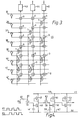
- the digital code detector circuit shown ia Figure 1 comprises an array of ten gating transistors 1 to 10 connected between two pairs of drive transistors 11/13 and 12/14 across supply rails (+V), (0V).
- the array is fed with true data signals from a set of four input leads 15 to 18. These true data signals can have either a high logic level or a low logic level, corresponding to logic levels 1 and 0, respectively.
- Inverse data signals which are derived from the true data signals by respective inverters 19 to 22 are also fed to the array.
- the array feeds two output circuits 23 and 24, each of which includes an input storage capacitor 25, 26, as will be considered in detail later in the specification.
- the drive transistors 11,12 and 13,14 receive pulses K2 and K1, respectively, at their gates. These pulses K2 and K1 are two phase in that they occur alternately without overlap in time. The occurrence of a pulse K2 switches on transistors 11 and 12 for the period of this pulse and the capacitors 25 and 26 are both pre-charged to the voltage +V which corresponds to the high logic level. On the occurrence of the immediately following pulse K1, both the transistors 13 and 14 are switched on, by which time the transistors 11 and 12 will be switched off again. In dependence on the logic levels at the set of input leads 15 to 18, different combinations of the transistors 1 to 10 can be switched on and off to complete or not a number of paths through the array.
- the transistors 1 to 10 can be enhancement type IGFETS. At each of the intersections in the array where two crossover leads are electrically insulated from each other, depletion type IGFETS can be used to form the intersection.
- FIG. 1 A convenient way of illustrating the circuit of Figure 1 is by means of a schematic diagram of the form shown in Figure 2.
- the gating transistors forming the array are represented by the small rectangles 1 to 10, respectively.
- the output circuits 23, 24 each receive a low logic level in response to "gated" high logic levels (i.e. when a discharge path 11/13 or 12/14 is completed) the input 31, 32 to each output circuit is given an "inverter" circle to signify that the low logic level corresponds to a binary 1 input signal.
- the circuit represented by the schematic diagram of Figure 2 is for detecting any one of the four code combinations 1000, 0100, 0010 and 0001 as represented by the logic levels of the true data signals applied to the set of four input leads 15, 16, 17 and 18 either singly, or two or more concurrently. Where two or more of the code combinations occur concurrently, the one which effectively has the highest binary numerical value is selected in preference to the other code combination(s).
- the selection takes the form of a 2-bit binary code which is produced as a priority address code by the two output circuits 23 and 24. It will be apparent that for the concurrent application of one, two, three or all four of the code combinations to the set of input leads, the effective logic levels on these leads will consist of all possible combinations of 1 and 0 logic levels of a 4-bit code. These combinations will effect logic gating within the circuit as set in the forth in the following TABLE 1.
- the four bona fide code combinations 1000, 0100, 0010 and 0001 are detected as binary address code 00, 01, 10 and 11 respectively. Also only one of these four possible binary address codes is produced, whatever effective input code combination obtains. Furthermore, the particular binary code which is produced is selected on a priority basis, depending which of the four bona fide code combinations are present concurrently. For instance, when 1000 is present, the binary address code is always 00, irrespective of whether one or more of 0100, 0010 and 0001 are also present (i.e. to give 1100, 1010 1001 etc., as the effective input combination). Similarly, when 0100 is present, the binary address code is always 01, whatever other bona fide code combinations are also present, and so on.
- the schematic diagram of Figure 3 represents a digital code detector circuit according to the invention which has a set of eight input leads 35 to 42 and a logic gating arrangement LG to detect the eight code combinations 10000000; 01000000; ... 00000001 having a single 1-bit. Because a 3-bit digital code is required for the eight possible binary code addresses, three output circuits 43 to 45 are provided.
- Table II gives the eight input code combinations with their respective binary code addresses.
- the first input lead (15 or 35) of a digital code detector arrangement according to the invention has for each output circuit a gate which is enabled by the inverse logic level
- the last input lead (18 or 42) has for each output circuit a gate which is enabled by the true logic level
- each of the intermediate input leads (16-17; 36-41) has for each output circuit a gate which is enabled by the inverse logic level
- a further gate which is enabled by the true logic level these further gates being positioned in correspondence with the particular binary code address which is allocated to the input code combination having the single bit of the high logic level for enabling these further gates.
- Figure 4 shows a typical two-phase dynamic circuit which can be used as the output circuits and which is operable synchronously with an array logic structure.
- the circuit shown in Figure 4 comprises both enhancement and depletion type insulated gate field effect transistors and is assumed to be implemented as an integrated circuit structure using n-channel technology. For this assumption, the array logic structures with which it is associated would, of course, be implemented using the same technology.
- Supply rails 46 and 47 of the circuit are connected across a supply voltage (+V), (0V).
- the circuit has an input stage comprised by two transistors 48 and 49, an intermediate stage comprised by two transistors 50 and 51, and an output stage comprised by two transistors 52 and 53.
- a first transfer transistor 54 is connected between an input 55 and the input stage, and a second transfer transistor 56 is connected betwen the input stage and the output stage.
- the transistors 48, 50, 52, 54 and 56 are enhancement type IGFETS.
- the transistors 49, 51 and 53 are depletion type IGFETS and serve as loads for the transistors 48, 50 and 52, respectively.
- the circuit of Figure 4 is driven by the two clock pulses K1 and K2, of different phases, which are used to drive an associated array logic structure. These clock pulses K1 and K2 are applied respectively to the gates of the transfer transistors 54 and 56.
- the transfer transistor 54 On the occurrence of a clock pulse K1, the transfer transistor 54 is switched on and the prevailing logic level at the input 55 is transferred to the gate of the transistor 48.
- the transfer transistor 54 is switched off and the prevailing logic level is maintained at the gate of the transistor 48 by a capacitor 58.
- the transistor 48 is switched on, or remains switched off, according as the prevailing logic level at the input 55 is the high logic level or the low logic level, to provide the alternate logic level at the junction of transistors 48/49.
- the transfer transistor 56 is switched on and said alternate logic level is transferred to the gate of the transistor 50.
- the transfer transistor 56 is switched off and said alternate level is maintained at the gate of the transistor 50 by a capacitor 59.
- the transistor 50 is switched on, or remains switched off, according as said alternate logic level is the high logic level or the low logic level.
- the transistor 52 has its gate connected to the junction of transistors 50/51 and thus provides the alternate logic level at the output 57.
- a capacitor 60 is provided to compensate for possible degradation of the logic level at the input 55.
- the capacitors 58, 59 and 60 are shown in dotted lines, because it is possible that each can be dispensed with if the gate capacitance of the relevant transistor suffices to perform their function.
Landscapes
- Engineering & Computer Science (AREA)
- Theoretical Computer Science (AREA)
- Physics & Mathematics (AREA)
- General Engineering & Computer Science (AREA)
- General Physics & Mathematics (AREA)
- Logic Circuits (AREA)
- Static Random-Access Memory (AREA)
Description
- This invention relates to digital code detector circuits of a kind suitable for detecting binary digital codes represented by a set of data signals in each of which a first logic level represents one binary value (say high =1) and a second logic level represents the opposite binary value (say low = 0).
- There are situations in digital circuit arrangements where of all the possible code combinations of an n-bit binary digital code with n>3, only those code combinations which contain only a single bit of one binary value (e.g. a single 1-bit) are used as identification codes. For instance, a plurality of memory circuits can have individual ones of those code combinations allocated to them, these code combinations being produced on a common set of identification leads for detection when their respective memory circuits are to be identified, for example for data read out.
- The organisation of a digital circuit arrangement may require that data is to be read out from only one of the memory circuits at a time. Therefore, if the code combinations for more than one of the memory circuits are present concurrently on the common set of identification leads, a selection of one of these code combinations becomes necessary to identify a particular memory circuit for data read out. However, when two or more of the code combinations are present concurrently, they corrupt one another to produce a resultant code combination containing two or more bits of said one binary value. This poses a problem in the detection of the bona fide code combinations which contain only a single bit of one binary value.
- A similar problem is dealt with in prior UK
patent specification 1 225 048 which relates to resolving the priority of parallel signals in electrical communication systems and in data processing systems. This prior UK patent specification describes apparatus which is operable to recognise the highest priority signal among signals on a multiplicity of communication channels and to encode the recognised signal. The apparatus has input means for receiving TRUE and NOT signals for each channel, output terminal means for the bit signals representing the number to be encoded, and encoding means electrically connected to said input means and to said output terminal means for receiving preselected TRUE and NOT channel signals from said input means and directly encoding the bit signals of the highest priority channel providing a signal. In the specific form of apparatus which is described in this prior UK patent specification, the encoding means has one group of coincidence gates for each bit of the bit signal. In order to simplify the logic, the TRUE and NOT channel signals are fed to these gates with a preselection appropriate for producing the ONE's complement of each of the bits of the highest priority channel number. No specific circuit implementation of the apparatus is given. - Prior USA
patent specification 3 825 888 relates to decoder circuits, and in particular to such circuits which are implemented using insulated gate field effect transistors (IGFETS). The circuit arrangements described in this prior USA patent specification form gate configurations which comprise series and/or parallel combinations of IGFETS which are switched selectively in response to TRUE and NOT input signals to produce decoded output signals. However, none of these gate configurations is suitable for recognising and responding to the highest priority input signal among a number of simultaneously applied input signals. - It is an object of the present invention to provide a digital code detector circuit which can detect on a priority basis one of a number of simultaneously applied input signals, and which comprises gate configurations requiring simpler logic than uaed for the apparatus described in the above-identified UK patent specification.
- It is a further object of the present invention to form the required gate configurations using an advantageous arrangement of IGFETS.
- According to the invention, there is provided a digital code detector circuit of the kind set forth above which is arraned to detect only those combinations of an n-bit binary code with n>3 which contain only a single bit of one binary value; which digital code detector circuit comprises a set of n-input leads for receiving 1 to n of these n input code combinations concurrently, inverter means for producing a set of inverse data signals whose logic levels are opposite to those of a received true set of data signals as made up from 1 to n of said input code combinations, a plurality m of output circuits for producing binary output address codes, where m is the number of bits required in an output address code to provide a unique m-bit output address code combination for each of the n input code combinations, and a gating arrangement which is for driving the output circuits and is operable to perform gating functions such that when more than one of the n input code combinations are present concurrently on the set of input leads, the output circuits are operated to produce the m-bit address code combination for the n-bit input code combination having the higher or highest binary value; and wbich digital code detector circuit is characterised in that said gating arrangement comprises in respect of each input lead of said set except that pertaining to the code combination of lowest priority, a number of m of first AND-gates which pertain respectively to the output circuits and which sre all enabled by an inverse data signal of said one binary value as derived by the relevant inverter means from a true data signal of opposite value applied to the input lead, the gating arrangement further comprising in respect of each input lead of said set, none, one or more second AND-gates for enabling by a true data signal of said one binary value applied to the input lead, these second gates pertaining respectively to those output circuits which are to provide a 1-bit in the address code combination for the particular input code combination which has said true data signal of said one binary value.
- It is to be understood that the word higher or highest as used above is to be interpreted in a relative sense having regard to which binary (logic) value is chosen to define the n input code combinations.
- A digital code detector circuit according to the invention is eminently suited for implementation as an integrated circuit that includes what will be termed an "array logic structure" which can be used to form so- called combinational logic circuits (that is, circuits whch can perform combinations of logic functions, such as AND and OR functions.
- For the purposes of the present specification an "array logic structure" is hereindefined as a plurality of controllable insulsted gate field effect transistors (IGFETS) which are formed at selected intersections of an array consisting of a plurality of rows of series-connected gate regions and a plurality of columns of surface regions which at each selected intersection define source and drain regions for the transistor which is formed there, an electrical path being formed at each other non-selected intersection, at least in use of the structure, to effectively short circuit the intersection in respect of the relevant surface column region.
- In one known form of this array logic structure, the controllable transistors at the selected intersections are formed as n-channel IGFETS of the enhancement type, and at the non-selected intersections there are formed n-channel IGFETS of the depletion type to provide the electrical paths which short circuit (or bridge) these latter intersections in the direction of the relevant surface region column. Further information concerning such an array logic structure can be found in United Kingdom
patent specification 1 575741. - In order that the invention may be more fully understood, reference will now be made by way of example to the accompanying drawings, of which:-
- Figure 1 shows one embodiment of a digital code detector circuit according to the invention;
- Figure 2 shows a schematic diagram of the circuit shown in Figure 1;
- Figure 3 shows a schematic diagram of another embodiment of a digital code detector circuit according to the invention; and
- Figure 4 shows an output circuit for the two embodiments.
- Referring to the drawings, the digital code detector circuit shown ia Figure 1 comprises an array of ten
gating transistors 1 to 10 connected between two pairs ofdrive transistors 11/13 and 12/14 across supply rails (+V), (0V). The array is fed with true data signals from a set of four input leads 15 to 18. These true data signals can have either a high logic level or a low logic level, corresponding tologic levels respective inverters 19 to 22 are also fed to the array. The array feeds twooutput circuits input storage capacitor - In operation of the circuit, the
drive transistors transistors capacitors transistors transistors transistors 1 to 10 can be switched on and off to complete or not a number of paths through the array. With thetransistors capacitors capacitors respective inverter output output circuit transistors 1 to 10 can be enhancement type IGFETS. At each of the intersections in the array where two crossover leads are electrically insulated from each other, depletion type IGFETS can be used to form the intersection. - A convenient way of illustrating the circuit of Figure 1 is by means of a schematic diagram of the form shown in Figure 2. In this schematic diagram, which will now be used to further describe the operation of the digital code detector circuit, the gating transistors forming the array are represented by the
small rectangles 1 to 10, respectively. At each intersection of the array where no gating transistor is provided, electrical isolation between the two crossover leads is assumed. Because theoutput circuits discharge path 11/13 or 12/14 is completed) theinput output - The circuit represented by the schematic diagram of Figure 2 is for detecting any one of the four code combinations 1000, 0100, 0010 and 0001 as represented by the logic levels of the true data signals applied to the set of four input leads 15, 16, 17 and 18 either singly, or two or more concurrently. Where two or more of the code combinations occur concurrently, the one which effectively has the highest binary numerical value is selected in preference to the other code combination(s). The selection takes the form of a 2-bit binary code which is produced as a priority address code by the two
output circuits 
- It can be seen from this table that the four bona fide code combinations 1000, 0100, 0010 and 0001 are detected as
binary address code - The schematic diagram of Figure 3 represents a digital code detector circuit according to the invention which has a set of eight input leads 35 to 42 and a logic gating arrangement LG to detect the eight code combinations 10000000; 01000000; ... 00000001 having a single 1-bit. Because a 3-bit digital code is required for the eight possible binary code addresses, three
output circuits 43 to 45 are provided. The following Table II gives the eight input code combinations with their respective binary code addresses.
- It can be seen that, in general, for a given address code priority order, the first input lead (15 or 35) of a digital code detector arrangement according to the invention has for each output circuit a gate which is enabled by the inverse logic level, the last input lead (18 or 42) has for each output circuit a gate which is enabled by the true logic level, and each of the intermediate input leads (16-17; 36-41) has for each output circuit a gate which is enabled by the inverse logic level, and for one or more of the output circuits a further gate which is enabled by the true logic level, these further gates being positioned in correspondence with the particular binary code address which is allocated to the input code combination having the single bit of the high logic level for enabling these further gates.
- For the sake of completeness in the description, Figure 4 shows a typical two-phase dynamic circuit which can be used as the output circuits and which is operable synchronously with an array logic structure. The circuit shown in Figure 4 comprises both enhancement and depletion type insulated gate field effect transistors and is assumed to be implemented as an integrated circuit structure using n-channel technology. For this assumption, the array logic structures with which it is associated would, of course, be implemented using the same technology. Supply rails 46 and 47 of the circuit are connected across a supply voltage (+V), (0V). The circuit has an input stage comprised by two
transistors 48 and 49, an intermediate stage comprised by twotransistors 50 and 51, and an output stage comprised by twotransistors first transfer transistor 54 is connected between aninput 55 and the input stage, and a second transfer transistor 56 is connected betwen the input stage and the output stage. Tbe output stage provides a high (1 = +V) logic level at anoutput 57 in response to a low (1 = 0V) logic level at theinput 55. Thetransistors transistors transistors 48, 50 and 52, respectively. - The circuit of Figure 4 is driven by the two clock pulses K1 and K2, of different phases, which are used to drive an associated array logic structure. These clock pulses K1 and K2 are applied respectively to the gates of the
transfer transistors 54 and 56. In operation of the circuit, theinput 55 is at either a high (0 = +V) logic level or a low (1 = 0V) logic level, as determined by the associated array logic structure, the operation of which corresponds to that described previously with reference to Figure 1. On the occurrence of a clock pulse K1, thetransfer transistor 54 is switched on and the prevailing logic level at theinput 55 is transferred to the gate of the transistor 48. At the end of the clock pulse K1, thetransfer transistor 54 is switched off and the prevailing logic level is maintained at the gate of the transistor 48 by a capacitor 58. The transistor 48 is switched on, or remains switched off, according as the prevailing logic level at theinput 55 is the high logic level or the low logic level, to provide the alternate logic level at the junction of transistors 48/49. On the occurrence of the immediately following clock pulse K2, the transfer transistor 56 is switched on and said alternate logic level is transferred to the gate of the transistor 50. At the end of the clock pulse K2, the transfer transistor 56 is switched off and said alternate level is maintained at the gate of the transistor 50 by acapacitor 59. The transistor 50 is switched on, or remains switched off, according as said alternate logic level is the high logic level or the low logic level. Thetransistor 52 has its gate connected to the junction of transistors 50/51 and thus provides the alternate logic level at theoutput 57. A capacitor 60 is provided to compensate for possible degradation of the logic level at theinput 55. Thecapacitors 58, 59 and 60 are shown in dotted lines, because it is possible that each can be dispensed with if the gate capacitance of the relevant transistor suffices to perform their function. - It has been stated above that the drawings illustrate examples of embodiments of the invention and, in order to avoid any misunderstanding, it is hereby further stated that, in the following claims, where technical features mentioned in any claim are followed by reference signs relating to features in the drawings and placed between parentheses, these reference signs have been included in accordance with Rule 29(7) EPC for the sole purpose of facilitating comprehension of the claim, by reference to an example.
Claims (3)
Applications Claiming Priority (2)
| Application Number | Priority Date | Filing Date | Title |
|---|---|---|---|
| GB08328622A GB2149160B (en) | 1983-10-26 | 1983-10-26 | Digital code detector circuit with priority |
| GB8328622 | 1983-10-26 |
Publications (3)
| Publication Number | Publication Date |
|---|---|
| EP0141464A2 EP0141464A2 (en) | 1985-05-15 |
| EP0141464A3 EP0141464A3 (en) | 1987-11-19 |
| EP0141464B1 true EP0141464B1 (en) | 1991-01-02 |
Family
ID=10550767
Family Applications (1)
| Application Number | Title | Priority Date | Filing Date |
|---|---|---|---|
| EP84201535A Expired EP0141464B1 (en) | 1983-10-26 | 1984-10-24 | Digital code detector circuits |
Country Status (5)
| Country | Link |
|---|---|
| US (1) | US4584567A (en) |
| EP (1) | EP0141464B1 (en) |
| JP (1) | JPS60121588A (en) |
| DE (1) | DE3483815D1 (en) |
| GB (1) | GB2149160B (en) |
Families Citing this family (7)
| Publication number | Priority date | Publication date | Assignee | Title |
|---|---|---|---|---|
| US4675556A (en) * | 1986-06-09 | 1987-06-23 | Intel Corporation | Binomially-encoded finite state machine |
| JPS64821A (en) * | 1987-06-23 | 1989-01-05 | Matsushita Electric Ind Co Ltd | Priority encoder |
| JP2632089B2 (en) * | 1990-06-07 | 1997-07-16 | 三菱電機株式会社 | Semiconductor circuit device |
| US5327128A (en) * | 1993-01-22 | 1994-07-05 | Cirrus Logic, Inc. | Compact glitchless M of N decoder circuit for digital to analog converters |
| JP3891587B2 (en) * | 1995-02-02 | 2007-03-14 | コーニンクレッカ フィリップス エレクトロニクス エヌ ヴイ | Combining video mosaic and teletext |
| JP2768301B2 (en) * | 1995-04-12 | 1998-06-25 | 日本電気株式会社 | Detection circuit |
| US5995016A (en) * | 1996-12-17 | 1999-11-30 | Rambus Inc. | Method and apparatus for N choose M device selection |
Family Cites Families (6)
| Publication number | Priority date | Publication date | Assignee | Title |
|---|---|---|---|---|
| US3251040A (en) * | 1961-12-01 | 1966-05-10 | Sperry Rand Corp | Computer input-output system |
| US3142056A (en) * | 1962-08-31 | 1964-07-21 | Gen Dynamics Corp | Analog-to-digital quantizer |
| US3284794A (en) * | 1963-02-06 | 1966-11-08 | Westinghouse Electric Corp | Parallel analog to digital converter |
| US3311881A (en) * | 1963-07-18 | 1967-03-28 | Bunker Ramo | Selection circuit responsive to plural inputs in a priority sequence |
| US3534339A (en) * | 1967-08-24 | 1970-10-13 | Burroughs Corp | Service request priority resolver and encoder |
| JPS5120787B1 (en) * | 1970-10-27 | 1976-06-28 |
-
1983
- 1983-10-26 GB GB08328622A patent/GB2149160B/en not_active Expired
-
1984
- 1984-10-24 DE DE8484201535T patent/DE3483815D1/en not_active Expired - Lifetime
- 1984-10-24 EP EP84201535A patent/EP0141464B1/en not_active Expired
- 1984-10-26 US US06/665,270 patent/US4584567A/en not_active Expired - Lifetime
- 1984-10-26 JP JP59224234A patent/JPS60121588A/en active Pending
Also Published As
| Publication number | Publication date |
|---|---|
| US4584567A (en) | 1986-04-22 |
| EP0141464A3 (en) | 1987-11-19 |
| GB2149160A (en) | 1985-06-05 |
| DE3483815D1 (en) | 1991-02-07 |
| GB8328622D0 (en) | 1983-11-30 |
| JPS60121588A (en) | 1985-06-29 |
| EP0141464A2 (en) | 1985-05-15 |
| GB2149160B (en) | 1987-02-11 |
Similar Documents
| Publication | Publication Date | Title |
|---|---|---|
| EP0072845B1 (en) | Memory system having memory cells capable of storing more than two states | |
| US4583197A (en) | Multi-stage pass transistor shifter/rotator | |
| US3691538A (en) | Serial read-out memory system | |
| US4506341A (en) | Interlaced programmable logic array having shared elements | |
| US4344005A (en) | Power gated decoding | |
| US4849935A (en) | Semiconductor memory including transparent latch circuits | |
| US4514829A (en) | Word line decoder and driver circuits for high density semiconductor memory | |
| US4194130A (en) | Digital predecoding system | |
| EP0440221B1 (en) | Priority encoder | |
| US4827160A (en) | Dynamic decoder circuit with charge-sharing prevention means | |
| US3222645A (en) | Magnetic parallel comparison means for comparing a test word with a plurality of stored words | |
| GB2091008A (en) | A semiconductor memory | |
| US4103349A (en) | Output address decoder with gating logic for increased speed and less chip area | |
| US4584567A (en) | Digital code detector circuits | |
| US3289169A (en) | Redundancy reduction memory | |
| EP0290042A2 (en) | Memory circuit with improved serial addressing scheme | |
| JPS6188619A (en) | D-A converter | |
| EP0060078B1 (en) | Read-only memory device | |
| US4069427A (en) | MIS logic circuit of ratioless type | |
| US3851186A (en) | Decoder circuit | |
| US4308526A (en) | Binary to one of N decoder having a true and a complement output | |
| US4931971A (en) | Partial decode shifter/rotator | |
| US4803649A (en) | Modulo-2-adder for the logic-linking of three input signals | |
| US4868788A (en) | Semiconductor memory device with improved word line drive circuit | |
| US4037217A (en) | Read-only memory using complementary conductivity type insulated gate field effect transistors |
Legal Events
| Date | Code | Title | Description |
|---|---|---|---|
| PUAI | Public reference made under article 153(3) epc to a published international application that has entered the european phase |
Free format text: ORIGINAL CODE: 0009012 |
|
| AK | Designated contracting states |
Designated state(s): DE FR GB IT SE |
|
| PUAL | Search report despatched |
Free format text: ORIGINAL CODE: 0009013 |
|
| AK | Designated contracting states |
Kind code of ref document: A3 Designated state(s): DE FR GB IT SE |
|
| 17P | Request for examination filed |
Effective date: 19880502 |
|
| RAP3 | Party data changed (applicant data changed or rights of an application transferred) |
Owner name: N.V. PHILIPS' GLOEILAMPENFABRIEKEN Owner name: PHILIPS ELECTRONIC AND ASSOCIATED INDUSTRIES LIMIT |
|
| 17Q | First examination report despatched |
Effective date: 19891124 |
|
| 17Q | First examination report despatched |
Effective date: 19900427 |
|
| GRAA | (expected) grant |
Free format text: ORIGINAL CODE: 0009210 |
|
| AK | Designated contracting states |
Kind code of ref document: B1 Designated state(s): DE FR GB IT SE |
|
| REF | Corresponds to: |
Ref document number: 3483815 Country of ref document: DE Date of ref document: 19910207 |
|
| ITF | It: translation for a ep patent filed | ||
| ET | Fr: translation filed | ||
| PGFP | Annual fee paid to national office [announced via postgrant information from national office to epo] |
Ref country code: SE Payment date: 19911028 Year of fee payment: 8 |
|
| PLBE | No opposition filed within time limit |
Free format text: ORIGINAL CODE: 0009261 |
|
| STAA | Information on the status of an ep patent application or granted ep patent |
Free format text: STATUS: NO OPPOSITION FILED WITHIN TIME LIMIT |
|
| 26N | No opposition filed | ||
| PG25 | Lapsed in a contracting state [announced via postgrant information from national office to epo] |
Ref country code: SE Effective date: 19921025 |
|
| EUG | Se: european patent has lapsed |
Ref document number: 84201535.6 Effective date: 19930510 |
|
| ITPR | It: changes in ownership of a european patent |
Owner name: CAMBIO RAGIONE SOCIALE;PHILIPS ELECTRONICS N.V. |
|
| REG | Reference to a national code |
Ref country code: FR Ref legal event code: CD |
|
| PGFP | Annual fee paid to national office [announced via postgrant information from national office to epo] |
Ref country code: GB Payment date: 19970930 Year of fee payment: 14 |
|
| PGFP | Annual fee paid to national office [announced via postgrant information from national office to epo] |
Ref country code: FR Payment date: 19971021 Year of fee payment: 14 |
|
| PGFP | Annual fee paid to national office [announced via postgrant information from national office to epo] |
Ref country code: DE Payment date: 19971219 Year of fee payment: 14 |
|
| REG | Reference to a national code |
Ref country code: FR Ref legal event code: CD |
|
| PG25 | Lapsed in a contracting state [announced via postgrant information from national office to epo] |
Ref country code: GB Free format text: LAPSE BECAUSE OF NON-PAYMENT OF DUE FEES Effective date: 19981024 |
|
| GBPC | Gb: european patent ceased through non-payment of renewal fee |
Effective date: 19981024 |
|
| PG25 | Lapsed in a contracting state [announced via postgrant information from national office to epo] |
Ref country code: FR Free format text: LAPSE BECAUSE OF NON-PAYMENT OF DUE FEES Effective date: 19990630 |
|
| REG | Reference to a national code |
Ref country code: FR Ref legal event code: ST |
|
| PG25 | Lapsed in a contracting state [announced via postgrant information from national office to epo] |
Ref country code: DE Free format text: LAPSE BECAUSE OF NON-PAYMENT OF DUE FEES Effective date: 19990803 |