EP0138439A2 - Electrically erasable programable nonvolatile semiconductor memory device having dual-control gate - Google Patents
Electrically erasable programable nonvolatile semiconductor memory device having dual-control gate Download PDFInfo
- Publication number
- EP0138439A2 EP0138439A2 EP84306502A EP84306502A EP0138439A2 EP 0138439 A2 EP0138439 A2 EP 0138439A2 EP 84306502 A EP84306502 A EP 84306502A EP 84306502 A EP84306502 A EP 84306502A EP 0138439 A2 EP0138439 A2 EP 0138439A2
- Authority
- EP
- European Patent Office
- Prior art keywords
- region
- semiconductor region
- data updating
- semiconductor
- potential
- Prior art date
- Legal status (The legal status is an assumption and is not a legal conclusion. Google has not performed a legal analysis and makes no representation as to the accuracy of the status listed.)
- Granted
Links
Images


Classifications
-
- G—PHYSICS
- G11—INFORMATION STORAGE
- G11C—STATIC STORES
- G11C16/00—Erasable programmable read-only memories
- G11C16/02—Erasable programmable read-only memories electrically programmable
- G11C16/04—Erasable programmable read-only memories electrically programmable using variable threshold transistors, e.g. FAMOS
- G11C16/0408—Erasable programmable read-only memories electrically programmable using variable threshold transistors, e.g. FAMOS comprising cells containing floating gate transistors
- G11C16/0416—Erasable programmable read-only memories electrically programmable using variable threshold transistors, e.g. FAMOS comprising cells containing floating gate transistors comprising cells containing a single floating gate transistor and no select transistor, e.g. UV EPROM
-
- H—ELECTRICITY
- H10—SEMICONDUCTOR DEVICES; ELECTRIC SOLID-STATE DEVICES NOT OTHERWISE PROVIDED FOR
- H10B—ELECTRONIC MEMORY DEVICES
- H10B69/00—Erasable-and-programmable ROM [EPROM] devices not provided for in groups H10B41/00 - H10B63/00, e.g. ultraviolet erasable-and-programmable ROM [UVEPROM] devices
Definitions
- the present invention relates to an electrically erasable programable nonvolatile semiconductor memory device having a dual-control gate.
- EEPROMs Electrically Erasable Programable Read-Only Memories
- dual-control gate type nonvolatile memory cells are widely adopted.
- a memory cell of this type electrons are injected by a tunnel current in an electrically insulated floating gate to update the memory contents.
- a high enough voltage e.g., 18 V to 25 V
- Each memory cell must have a high dielectric strength against such a high voltage. The requirement presents a big problem to achieve micropatterning and high performance of the memory cell.
- the dielectric strength of each cell is mainly determined by a p-n junction between a source or a drain and the substrate.
- the dielectric strength of the p-n junction depends on a surface breakdown between the source or the drain and the substrate. The surface breakdown tends to occur when a high write/erase voltage is applied to the control gate or the semiconductor region for data updating. In this case, the thickness of a depletion layer formed near a portion of the p-n junction which is in contact with a gate oxide film becomes small, and an electric field is concentrated therein.
- the thickness of the gate oxide film under the control gate must be increased, or a junction depth of the source or drain region must be increased. However, this condition prevents micropatterning of the cell.
- a low impurity concentration diffusion layer is formed in part of the source or drain region located adjacent to the control gate.
- a read rate is decreased and an operating margin is narrowed.
- an additional process for forming the low impurity concentration diffusion layer is required, and an extra area for this low impurity concentration diffusion layer is also required.
- an electrically erasable programable nonvolatile semiconductor memory device comprising: a first semiconductor region having a plurality of memory cells in a matrix form; a second semiconductor region having a peripheral circuit for controlling the plurality of memory cells; insulating means for electrically insulating the first semiconductor region from the second semiconductor region; and potential sustaining means for constantly sustaining a data updating region and the first semiconductor region at the same potential when the plurality of memory cells are selectively charged/discharged.
- Each memory cell has a floating gate, first and second control gates capacitively coupled to the floating gate, source and drain regions, and the data updating region continuously formed with the source or drain region to exchange a charge with the floating gate by a tunnel effect.
- the data updating region has a conductivity type opposite to that of the first semiconductor region.
- the first and second control gates of the respective memory cells are commonly connected along directions perpendicular to each other in the matrix form.
- an electric field applied to the p-n junction formed by the first semiconductor region and the data updating region for exchanging electrons with the floating gate can be weakened.
- the first semiconductor region is electrically insulated from the second semiconductor region by the insulating means of high dielectic strength. Therefore, the surface breakdown phenomenon at the memory cell section can be prevented, and the device as a whole can have a high dielectric strength. For this reason, the read rate of the memory cells will not be lowered.
- the memory cells can be micropatterned and highly integrated without a complicated fabrication process.
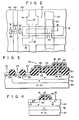
- Fig. 1 shows an EEPROM according to the present invention.
- the EEPROM has a memory cell array 12, and the memory cell array 12 has a plurality of memory cells 10 in a matrix form on a single chip.
- Each memory cell 10 has source and drain regions 14 and 16, a first control gate 18, a second control gate 20, a floating gate 22 and a data updating region 24 for exchanging electrons with the floating gate 22.
- the substrate regions of the respective memory cells 10 are constituted by a common semiconductor region 30.
- the first and second control gates 18 and 20 are capacitively coupled to the floating gate 22.
- the first control gate 18 is connected to an X decoder 26, and the second control gate 20 is connected to a Y decoder 28.
- each memory cell 10 has the first and second control gates 18 and 20 which are respectively selected by the X and Y decoders 26 and 28, the cell 10 is called a dual-control gate cell (DC cell).
- DC cell dual-control gate cell
- the single chip also has a read/write circuit 32 for reading out data from or writing it in the memory cell 10, a high voltage circuit (H.V. CKT) 34 for generating high voltages needed for injecting electrons in or extracting them from the floating gate 22 in the memory cell 10, and a terminal 36.
- the X decoder 26, the Y decoder 28, the read/write circuit 32, the high voltage circuit 34, and the terminal 36 constitute a peripheral circuit. This peripheral circuit is formed in another semiconductor region electrically insulated from the semiconductor region 30.
- the construction of the memory cell in the peripheral portion of the substrate will be described with reference to Figs. 2 to 4. Only one memory cell in the peripheral portion of the substrate is shown for illustrative convenience. In practice, all of a plurality of memory cells in a matrix form are formed within the p-type semiconductor region 30.
- An n-type isolation layer 42 is formed in a p-type Si substrate 40, and the p-type semiconductor region 30 is formed on the.n-type isolation layer 42.
- the p-type semiconductor region 30 is surrounded by the n-type isolation layer 42 and is electrically insulated from the substrate 40.
- the plurality of DC cells 10 are formed in the p-type semiconductor region 30.
- the DC cells 10 are generally arranged in a matrix form.
- Each memory cell 10 comprises the n-type source region 14, the n-type drain region 16, the n-type data updating region 24 connected to the drain region 16, the first control gate 18, the second control gate 20, the floating gate 22, and gate oxide films 44, 46, 48 and 50.
- the source region 14, the drain region 16, and the data updating region 24 are formed in the p-type semiconductor region 30.
- the second control gate 20 is formed above the floating gate 22, and the first control gate 18 is formed on the second control gate 20.
- the gate oxide film 44 is formed between the channel region and the floating gate. 22.
- the gate oxide film 46 is formed between the channel region and the first control gate 18, between the drain region 16 and the first control gate 18 and between the floating gate 22 and the first control gate 18.
- the gate oxide film 48 is formed between the second control gate 20 and the first control gate 18.
- the gate oxide film 50 is formed between the data updating region 24 and the floating gate 22.
- a potential Va is supplied to the p-type semiconductor region 30 through a p + -type diffusion layer 52.
- a potential V b is supplied to the n-type isolation layer 42 through an n + -type diffusion layer 54.
- a potential Vc is supplied to the semiconductor substrate 40 through a p + -type diffusion layer 56.
- a potential Vs is supplied to the drain region 16 and the data updating region 24.
- the write/erase operation of the memory cell 10 is performed as follows.
- Vc 0 V
- a high potential e.g., 20 V
- Electrons are then injected from the data updating region 24 to the floating gate 22 due to the tunnel effect.
- a voltage is not applied across the p-n junctions formed between the drain region 16 and the p-type semiconductor region 30 and between the data updating region 24 and semiconductor region 30, thus preventing the surface breakdown.
- a voltage is not applied between the n-type isolation layer 42 and the p-type Si substrate 40, thus preventing the breakdown between the n-type isolation layer 42 and the p-type Si substrate 40.
- the electrons are shifted from the floating gate 22 to the data updating region 24 by the tunnel effect, thereby completing electron emission.
- no breakdown occurs since a voltage is not applied across the p-n junctions formed between the drain region 16 and the p-type semiconductor region 30 and between the data updating region 24 and the p-type semiconductor region 30, no breakdown occurs.
- an n -type layer may be inserted to constitute a p-n junction with the substrate.
- the packing density of the device will not be decreased.
- an n-type impurity such as arsenic or phosphorus may be ion-implanted in the p-type Si substrate 40 at an acceleration voltage of 200 to 1,000 kV to form the n-type isolation layer 42 and the p-type semiconductor region 30.
- an n-type layer may be formed on the p-type substrate 40 by ion implantation or diffusion, a p-type epitaxial layer may be formed thereon, and ion implantation or diffusion is performed with respect to the n-type layer, thereby forming the n-type isolation layer 42 and the p-type semiconductor region 30.
- a highly integrated EEPROM having a high dielectric strength can be obtained according to this embodiment of the present invention.
- the thickness of the oxide film of the memory cell and the junction depth can be freely selected in accordance with micropatterns of the memory cells based on the scaling rules.
- the present invention is very effective for micropatterning the memory cells. Unlike the conventional device wherein the dielectric strength is increased by a low impurity concentration diffusion layer, the fabrication process will not be complicated and the read characteristics of the memory cells will not be degraded.
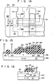
- an electrically erasable programable nonvolatile semiconductor memory device will be described with reference to Figs. 5 to 7.
- an insulating layer 60 made of silicon oxide (Si0 2 ) is formed between a p-type Si substrate 40 and a p-type common semiconductor region 30. Therefore, the p-type semiconductor region 30 is electrically insulated. from the p-type Si substrate 40.
- Oxygen is ion-implanted in the p-type substrate 40 at a dose of 1 x 10 17 /cm 2 and at an acceleration voltage of 200 kV, and the resultant structure is annealed in a nitrogen atmosphere at a temperature of 1,000°C for about an hour, thereby forming a buried oxide layer 62.
- the p-type Si substrate 40 is then selectively oxidized to form an oxide region 64 connected to the oxide layer 62, thereby preparing the insulating layer 60.
- Any other arrangement of the second embodiment is substantially the same as that of the first embodiment.
- the same reference numerals as in the second embodiment denote the same parts as in the first embodiment, and a detailed description will be omitted.
- the write/erase operation of the memory cell will be performed as follows.
- the Si substrate 40 is set at a fixed potential Vc of 0 V.
- Vc 0 V
- the condition Va 0 V is established
- the data updating region 24 is set at a potential Vs of 0 V
- a high potential e.g., 20 V
- the electrons are then injected from the data updating region 24 to the floating gate 22 by the tunnel effect.
- a high voltage is not applied across p-n junctions between a drain region 16 and a p-type semiconductor region 30 and between the data updating region 24 and a p-type semiconductor region 30, thereby preventing the surface breakdown effect.
- the p-type semiconductor region 30 is electrically insulated from the p-type Si substrate 40 through the insulating layer 60, no breakdown occurs.
- the electrons are shifted from the floating gate 22 to the data updating region 24 by the tunnel effect.
- no voltage is applied across p-n junctions between the drain region 16 and the p-type semiconductor region 30 and between the data updating region 24 and the p-type semiconductor region 30, thereby preventing the breakdown phenomenon.
- the p-type semiconductor region 30 and the p-type Si substrate 40 are set at 20 V and 0 V, respectively. However, since the p-type semiconductor region 30 is isolated by the insulating layer 60 from the p-type Si substrate 40, no breakdown occurs.
- a first semiconductor region 72 and a second semiconductor region 74 are formed on an insulating substrate 70 made of, for example, sapphire.
- the first and second semiconductor regions 72 and 74 constitute silicon islands and are. isolated by an insulating region 76.
- a plurality of memory cells are formed in the first semiconductor region 72 in the same manner as the previous embodiments.
- a peripheral circuit is formed in the second semiconductor region 74.
- the cell arrangement of the third embodiment is substantially the same as those of the first and second embodiments.
- the same reference numerals as in the third embodiment denote the same parts as in first and second embodiments, and a detailed description thereof will be omitted.
- a voltage (e.g., 20 V) is applied between a floating gate 22 and a data updating region 24.
- the n-type data updating region 24 is kept at the same potential as that of the p-type first semiconductor region 72.
- a potential Vs at the n-type data updating region 24 is the same as a potential Va at the first semiconductor region 72. Since no voltage is applied across a p-n junction between the data updating region 24 and the first semiconductor region 72, no surface breakdown will occur in this p-n junction.
- a potential Vc at the second semiconductor region 74 is normally 0 V.
- the first semiconductor region 72 is electrically insulated from the second semiconductor region 74 through the insulating substrate 70 and the insulating region 76, thus preventing the breakdown phenomenon. According to the third embodiment, the same effect as in the first embodiment can be obtained.
- All cells 10 are formed in a p-type well region 82 in an n-type Si substrate 80 in this embodiment.
- the p-type well region 82 is electrically insulated from the n-type Si substrate 80 through a p-n junction 81 formed between the p-type well region 82 and the n-type Si substrate 80.
- Each memory cell 10 comprises an n-type source region 14, an n-type drain region 16, an n-type data updating region 24 connected to the drain region 16, a first control gate 18, a second control gate 20, a floating gate 22, and gate oxide films 44, 46, 48 and 50.
- the source region 14, the drain region 16, and the data updating region 24 are formed in the p-type well region 82.
- the second control gate 20 is formed above the floating gate 22, and the first control gate 18 is formed above the second control gate 20.
- the gate oxide film 44 is formed between a channel region and the floating gate 22.
- the gate oxide film 46 is formed between the channel region and the first control gate 18, between the drain region 16 and the first control gate 18 and between the floating gate 22 and the first control gate 18.
- the gate oxide film 48 is formed between the second control gate 20 and the first control gate 18.
- the gate oxide film 50 is formed between the data updating region 24 and the floating gate 22.
- a potential Va is applied to the p-type well region 82 through a p +- type diffusion layer 84, and a potential Vc is applied to the semiconductor substrate 80 through an n +- type diffusion layer 86.
- a potential Vs is applied to the drain region 16 and the data updating region 24.
- a potential Vc at the n-type Si substrate 80 is a fixed potential Vdd of +5 V.
- the first and second control gates 18 and 20 are set at a voltage of -15 V, and the data updating region 24 has a potential Vs of +5 V.
- the electrons are emitted from the floating gate 22 to the data updating region 24 by the tunnel effect, so that a threshold voltage of the memory cell 10 is shifted in the negative direction.
- the potential Va at the p-type well region 82 is .set to be equal to the potential Vs at the data updating region 24.
- the surface breakdown phenomenon tends to occur in a conventional device.
- the electric field is not concentrated, thereby preventing the breakdown phenomenon.
- one of the control gates is set at a potential of +5 V, a sufficient potential difference between the floating gate 22 and the data updating region 24 will not be generated, thus disabling emission of electrons.
- a case will be described wherein the electrons are injected from the data updating region 24 to the floating gate 22.
- the first and second gates 18 and 20 are set at a potential of +5 V
- the data updating region 24 and the p - type well region 82 are respectively set at potentials Vs and Va of -15 V.
- the electrons are injected from the data updating region 24 to the floating gate by the tunnel effect, so that the threshold voltage of the memory cell is shifted in the positive direction.
- the data updating region 24 and the p-type well region 82 are kept at the same potential, and no voltage is applied across the p-n junction therebetween, thereby preventing the surface breakdown phenomenon.
- the same effect as in the first embodiment can be obtained.
- the p-type well region 82 is formed by using the n-type substrate 80 in the fourth embodiment, a negative potential can be easily generated in the chip. A signal is decoded to easily apply this negative potential to only the necessary control gate. This is because this p-type well region 82 is electrically isolated through the n-type substrate 80 from another well region which is biased to 0 V. Therefore, the p-type well region 82 is charged to generate the negative potential within the chip.
- memory cells 110 comprise p-channel memory cells. All the memory cells 110 are formed in an n-type well region 182 in a p-type Si substrate 180.
- the n-type well region 182 is electrically isolated from the p-type Si substrate 180 through a p-n junction 181 between the n-type well region 182 and the p-type Si substrate 180.
- Each memory cell 110 comprises a p-type source region 114, a p-type drain region 116, a p-type data updating region 124 connected to the drain region 116, a first control gate 118, a second control gate 120, a floating gate 122, and gate oxide films 144, 146, 148 and 150.
- the source region 114, the drain region 116, and the data updating region 124 are formed within the n-type well region 182.
- the second control gate 120 is formed above the floating gate 122, and a first control gate 118 is formed above the second control gate 120.
- the gate oxide film 144 is formed between the channel region and the floating gate 122.
- the gate oxide film 146 is formed between the channel region and the first control gate 118, between the drain region 116 and the first control gate 118 and between the floating gate 122 and the first control gate 118.
- the gate oxide film 148 is formed between the second control gate 120 and the first control gate 118.
- the gate oxide film 150 is formed between the data updating region 124 and the floating gate 122.
- a potential Va is applied to the n-type well region 182 through an n +- type diffusion layer 184, and a potential Vc is applied to the semiconductor substrate 180 through a p +- type diffusion layer 186.
- a potential Vs is applied to the drain region 116 and the data updating region 124.
- the potential Vc at the substrate is a fixed potential Vss of 0 V.
- the first and second control gates 118 and 120 are set at a potential of +20 V, and the potential Vs at the data updating region 124 is the ground potential of 0 V.
- the electrons are injected from the data updating region 24 to the floating gate 122 by the tunnel effect, so that the threshold voltage of the memory cell 110 is shifted in the positive direction.
- the potential Va at the n-type well region 182 is the same as the potential Vs at the data updating region 124.
- the thickness of the depletion layer is thin at a portion 188 located in a position where the p-n junction is in contact with the gate oxide film 146, and thus the electric field is concentrated therein. Therefore, according to the conventional device, the surface breakdown phenomenon tends to occur. However, according to the device of the present invention, since a voltage is not applied across the p-n junction, the electric field is not concentrated, thereby completely preventing the breakdown phenomenon. When one of the control gates is set at 0 V, a sufficient potential difference between the floating gate 122 and the data updating region 124 does not occur, thereby disabling the injection of the electrons.
- a case will be described wherein electrons are emitted from the floating gate 122 to the data updating region 124.
- the first and second control gates 118 and 120 are set at 0 V, and the potential Vs at the data updating region 124 and the potential Va at the n-type well region 182 are set at a potential of 20 V.
- the electrons are emitted from the floating gate 122 to the data updating region 124 by the tunnel effect, so that the threshold voltage of the memory cell 110 is shifted in the negative direction.
- the data updating region 124 and the n-type well region 182 are kept at the same potential. As a result, no voltage is applied to the p-n junction between the regions 124 and 182, and thus the surface breakdown phenomenon is prevented.
- a p-n junction 181 between the n-type well region 182 and the p-type Si substrate 180 receives a potential of 20 V.
- the dielectric withstand voltage of the n-type well region 182 can be more than 20 V irrespective of micropattering of the memory cells. Therefore, no breakdown phenomenon will occur.
- the position of the source may be replaced with that of the drain.
- the high voltage for data write/erase operation is not limited to the value exemplified in the above embodiments. The scope of the present invention will not essentially change even if any other potential is used.
Abstract
Description
- The present invention relates to an electrically erasable programable nonvolatile semiconductor memory device having a dual-control gate.
- In recent EEPROMs (Electrically Erasable Programable Read-Only Memories), dual-control gate type nonvolatile memory cells are widely adopted. In a memory cell of this type, electrons are injected by a tunnel current in an electrically insulated floating gate to update the memory contents. In order to selectively write data in or erase it from these EEPROM cells, a high enough voltage (e.g., 18 V to 25 V) to induce the tunnel current must be selectively applied to the dual-control gate of a desired cell or a semiconductor region for data updating. Each memory cell must have a high dielectric strength against such a high voltage. The requirement presents a big problem to achieve micropatterning and high performance of the memory cell.
- The dielectric strength of each cell is mainly determined by a p-n junction between a source or a drain and the substrate. The dielectric strength of the p-n junction depends on a surface breakdown between the source or the drain and the substrate. The surface breakdown tends to occur when a high write/erase voltage is applied to the control gate or the semiconductor region for data updating. In this case, the thickness of a depletion layer formed near a portion of the p-n junction which is in contact with a gate oxide film becomes small, and an electric field is concentrated therein. In order to increase the surface breakdown voltage, the thickness of the gate oxide film under the control gate must be increased, or a junction depth of the source or drain region must be increased. However, this condition prevents micropatterning of the cell. In order to solve this problem, a low impurity concentration diffusion layer is formed in part of the source or drain region located adjacent to the control gate.. However, according to this technique, a read rate is decreased and an operating margin is narrowed. In addition to these disadvantages, an additional process for forming the low impurity concentration diffusion layer is required, and an extra area for this low impurity concentration diffusion layer is also required.
- It is an object of the present invention to provide an electrically erasable programable nonvolatile semiconductor memory device wherein a sufficiently high dielectric strength can be guaranteed, and memory cells can be micropatterned and highly integrated.
- In order to achieve the above object of the present invention, there is provided an electrically erasable programable nonvolatile semiconductor memory device comprising: a first semiconductor region having a plurality of memory cells in a matrix form; a second semiconductor region having a peripheral circuit for controlling the plurality of memory cells; insulating means for electrically insulating the first semiconductor region from the second semiconductor region; and potential sustaining means for constantly sustaining a data updating region and the first semiconductor region at the same potential when the plurality of memory cells are selectively charged/discharged. Each memory cell has a floating gate, first and second control gates capacitively coupled to the floating gate, source and drain regions, and the data updating region continuously formed with the source or drain region to exchange a charge with the floating gate by a tunnel effect. The data updating region has a conductivity type opposite to that of the first semiconductor region. The first and second control gates of the respective memory cells are commonly connected along directions perpendicular to each other in the matrix form.
- According to the present invention, an electric field applied to the p-n junction formed by the first semiconductor region and the data updating region for exchanging electrons with the floating gate can be weakened. The first semiconductor region is electrically insulated from the second semiconductor region by the insulating means of high dielectic strength. Therefore, the surface breakdown phenomenon at the memory cell section can be prevented, and the device as a whole can have a high dielectric strength. For this reason, the read rate of the memory cells will not be lowered. In addition to this advantage, the memory cells can be micropatterned and highly integrated without a complicated fabrication process.
- Other objects and advantages will be apparent from the following description taken in conjunction with the accompanying drawings, in which:
- Fig. 1 is a plan view showing the layout of an electrically erasable programable nonvolatile semiconductor memory according to the present invention;
- Fig. 2 is a partial plan view of an electrically erasable programable nonvolatile semiconductor memory device according to a first embodiment of the present invention;
- Fig. 3 is a sectional view of the device taken along the line III - III of Fig. 2;
- Fig. 4 is a sectional view of the device taken along the line IV - IV of Fig. 2;
- Fig. 5 is a partial plan view of an electrically erasable programable nonvolatile semiconductor memory device according to a second embodiment of the present invention;
- Fig. 6 is a sectional view of the device taken along the line VI - VI of Fig. 5;
- Fig. 7 is a sectional view of the device taken along the line VII - VII of Fig. 5;
- Fig. 8 is a partial plan view of an electrically erasable programable nonvolatile semiconductor memory device according to a third embodiment of the present invention; .
- Fig. 9 is a sectional view of the device taken along the line IX - IX of Fig. 8;
- Fig. 10 is a sectional view of the device taken along the line X - X of Fig. 8;
- Fig. 11 is a partial plan view of an electrically erasable programable nonvolatile semiconductor memory device according to a fourth embodiment of the present invention;
- Fig. 12 is a sectional view of the device taken along the line XII - XII of Fig. 11;
- Fig. 13 is a sectional view of the device taken along the line XIII - XIII of Fig. 11;
- Fig. 14 is a partial plan view of an electrically erasable programable nonvolatile semiconductor memory device according to a fifth embodiment of the present invention;
- Fig. 15 is a sectional view of the device taken along the line XV - XV of Fig. 14; and
- Fig. 16 is a sectional view of the device taken along the line XVI - XVI of Fig. 14.
- Fig. 1 shows an EEPROM according to the present invention. The EEPROM has a
memory cell array 12, and thememory cell array 12 has a plurality ofmemory cells 10 in a matrix form on a single chip. Eachmemory cell 10 has source and drainregions first control gate 18, asecond control gate 20, a floatinggate 22 and adata updating region 24 for exchanging electrons with the floatinggate 22. The substrate regions of therespective memory cells 10 are constituted by acommon semiconductor region 30. The first andsecond control gates gate 22. Thefirst control gate 18 is connected to anX decoder 26, and thesecond control gate 20 is connected to aY decoder 28. Since eachmemory cell 10 has the first andsecond control gates Y decoders cell 10 is called a dual-control gate cell (DC cell). In the EEPROM having a plurality of DC cells, electron exchange between the floatinggate 22 and thedata updating region 24 is performed only in thememory cell 10 where its first andsecond control gates write circuit 32 for reading out data from or writing it in thememory cell 10, a high voltage circuit (H.V. CKT) 34 for generating high voltages needed for injecting electrons in or extracting them from the floatinggate 22 in thememory cell 10, and a terminal 36. TheX decoder 26, theY decoder 28, the read/write circuit 32, thehigh voltage circuit 34, and the terminal 36 constitute a peripheral circuit. This peripheral circuit is formed in another semiconductor region electrically insulated from thesemiconductor region 30. - The construction of the memory cell in the peripheral portion of the substrate will be described with reference to Figs. 2 to 4. Only one memory cell in the peripheral portion of the substrate is shown for illustrative convenience. In practice, all of a plurality of memory cells in a matrix form are formed within the p-
type semiconductor region 30. An n-type isolation layer 42 is formed in a p-type Si substrate 40, and the p-type semiconductor region 30 is formed on the.n-type isolation layer 42. The p-type semiconductor region 30 is surrounded by the n-type isolation layer 42 and is electrically insulated from thesubstrate 40. The plurality ofDC cells 10 are formed in the p-type semiconductor region 30. TheDC cells 10 are generally arranged in a matrix form. Eachmemory cell 10 comprises the n-type source region 14, the n-type drain region 16, the n-typedata updating region 24 connected to thedrain region 16, thefirst control gate 18, thesecond control gate 20, the floatinggate 22, andgate oxide films source region 14, thedrain region 16, and thedata updating region 24 are formed in the p-type semiconductor region 30. Thesecond control gate 20 is formed above thefloating gate 22, and thefirst control gate 18 is formed on thesecond control gate 20. Thegate oxide film 44 is formed between the channel region and the floating gate. 22. Thegate oxide film 46 is formed between the channel region and thefirst control gate 18, between thedrain region 16 and thefirst control gate 18 and between the floatinggate 22 and thefirst control gate 18. Thegate oxide film 48 is formed between thesecond control gate 20 and thefirst control gate 18. Thegate oxide film 50 is formed between thedata updating region 24 and the floatinggate 22. A potential Va is supplied to the p-type semiconductor region 30 through a p+ -type diffusion layer 52. A potential Vb is supplied to the n-type isolation layer 42 through an n+-type diffusion layer 54. A potential Vc is supplied to thesemiconductor substrate 40 through a p+-type diffusion layer 56. A potential Vs is supplied to thedrain region 16 and thedata updating region 24. - The write/erase operation of the
memory cell 10 is performed as follows. TheSi substrate 40 is set at a fixed potential Vc = 0 V. When electrons are injected from thedata updating region 24 to the floatinggate 22 of thememory cell 10, the condition Va = Vb = 0 V is established, and thedata updating region 24 is set at the potential Vs of 0 V. A high potential (e.g., 20 V) is applied to the first andsecond control gates data updating region 24 to the floatinggate 22 due to the tunnel effect. In this case, a voltage is not applied across the p-n junctions formed between thedrain region 16 and the p-type semiconductor region 30 and between thedata updating region 24 andsemiconductor region 30, thus preventing the surface breakdown. Similarly, a voltage is not applied between the n-type isolation layer 42 and the p-type Si substrate 40, thus preventing the breakdown between the n-type isolation layer 42 and the p-type Si substrate 40. - On the other hand, when the electrons are removed from the floating
gate 22 to thedata updating region 24, the first andsecond control gates gate 22 to thedata updating region 24 by the tunnel effect, thereby completing electron emission. In this case, since a voltage is not applied across the p-n junctions formed between thedrain region 16 and the p-type semiconductor region 30 and between thedata updating region 24 and the p-type semiconductor region 30, no breakdown occurs. On the other hand, since the p-type Si substrate 40 is set at the potential Vc = 0 V, a high voltage of 20 V is applied across the p-n junction formed by thesubstrate 40 and the n-type isolation layer 42. It is, however, very easy to increase the dielectric strength of this p-n junction. Even if the junction depth of the n-type isolation layer 42 is as deep as 2 to 10 µm, element characteristics and its micropatterning will not be influenced by the increase in junction depth. Therefore, the dielectric withstand voltage of the p-n junction between thesubstrate 40 and the n-type isolation layer 42 can become more than 30 V. Alternatively, for obtaining a higher dielectric strength, an n -type layer may be inserted to constitute a p-n junction with the substrate. In this case, unlike the conventional case wherein the respective memory cells have a high dielectric withstand voltage, the packing density of the device will not be decreased. - In order to form such a semiconductor structure, an n-type impurity such as arsenic or phosphorus may be ion-implanted in the p-
type Si substrate 40 at an acceleration voltage of 200 to 1,000 kV to form the n-type isolation layer 42 and the p-type semiconductor region 30. Alternatively, an n-type layer may be formed on the p-type substrate 40 by ion implantation or diffusion, a p-type epitaxial layer may be formed thereon, and ion implantation or diffusion is performed with respect to the n-type layer, thereby forming the n-type isolation layer 42 and the p-type semiconductor region 30. - A highly integrated EEPROM having a high dielectric strength can be obtained according to this embodiment of the present invention. In addition to this advantage, since the surface breakdown phenomenon of the memory cell can be effectively prevented, the thickness of the oxide film of the memory cell and the junction depth can be freely selected in accordance with micropatterns of the memory cells based on the scaling rules. The present invention is very effective for micropatterning the memory cells. Unlike the conventional device wherein the dielectric strength is increased by a low impurity concentration diffusion layer, the fabrication process will not be complicated and the read characteristics of the memory cells will not be degraded.
- An electrically erasable programable nonvolatile semiconductor memory device according to a second embodiment of the present invention will be described with reference to Figs. 5 to 7. According to the second embodiment, an insulating
layer 60 made of silicon oxide (Si02) is formed between a p-type Si substrate 40 and a p-typecommon semiconductor region 30. Therefore, the p-type semiconductor region 30 is electrically insulated. from the p-type Si substrate 40. Oxygen is ion-implanted in the p-type substrate 40 at a dose of 1 x 10 17 /cm 2 and at an acceleration voltage of 200 kV, and the resultant structure is annealed in a nitrogen atmosphere at a temperature of 1,000°C for about an hour, thereby forming a buriedoxide layer 62. The p-type Si substrate 40 is then selectively oxidized to form anoxide region 64 connected to theoxide layer 62, thereby preparing the insulatinglayer 60. Any other arrangement of the second embodiment is substantially the same as that of the first embodiment. The same reference numerals as in the second embodiment denote the same parts as in the first embodiment, and a detailed description will be omitted. - The write/erase operation of the memory cell will be performed as follows. The
Si substrate 40 is set at a fixed potential Vc of 0 V. In order to inject electrons from adata updating region 24 to a floatinggate 22 in thememory cell 10, the condition Va = 0 V is established, thedata updating region 24 is set at a potential Vs of 0 V, and a high potential (e.g., 20 V) is applied to first andsecond control gates data updating region 24 to the floatinggate 22 by the tunnel effect. In this case, a high voltage is not applied across p-n junctions between adrain region 16 and a p-type semiconductor region 30 and between thedata updating region 24 and a p-type semiconductor region 30, thereby preventing the surface breakdown effect. In addition, since the p-type semiconductor region 30 is electrically insulated from the p-type Si substrate 40 through the insulatinglayer 60, no breakdown occurs. - On the other hand, in order to emit the electrons from the floating
gate 22 to thedata updating region 24, the first andsecond control gates gate 22 to thedata updating region 24 by the tunnel effect. In this case, no voltage is applied across p-n junctions between thedrain region 16 and the p-type semiconductor region 30 and between thedata updating region 24 and the p-type semiconductor region 30, thereby preventing the breakdown phenomenon. The p-type semiconductor region 30 and the p-type Si substrate 40 are set at 20 V and 0 V, respectively. However, since the p-type semiconductor region 30 is isolated by the insulatinglayer 60 from the p-type Si substrate 40, no breakdown occurs. - According to the second embodiment, the same effect as in the first embodiment can be obtained.
- An electrically erasable programable nonvolatile semiconductor memory device according to a third embodiment of the present invention will be described with reference to Figs. 8 to 10. A
first semiconductor region 72 and asecond semiconductor region 74 are formed on an insulatingsubstrate 70 made of, for example, sapphire. The first andsecond semiconductor regions region 76. A plurality of memory cells are formed in thefirst semiconductor region 72 in the same manner as the previous embodiments. A peripheral circuit is formed in thesecond semiconductor region 74. The cell arrangement of the third embodiment is substantially the same as those of the first and second embodiments. The same reference numerals as in the third embodiment denote the same parts as in first and second embodiments, and a detailed description thereof will be omitted. - When electrons are exchanged between the floating
gate 22 and thedata updating region 24 in this EEPROM, a voltage (e.g., 20 V) is applied between a floatinggate 22 and adata updating region 24. In the case of the write/erase operation, the n-typedata updating region 24 is kept at the same potential as that of the p-typefirst semiconductor region 72. In other words, a potential Vs at the n-typedata updating region 24 is the same as a potential Va at thefirst semiconductor region 72. Since no voltage is applied across a p-n junction between thedata updating region 24 and thefirst semiconductor region 72, no surface breakdown will occur in this p-n junction. A potential Vc at thesecond semiconductor region 74 is normally 0 V. Thefirst semiconductor region 72 is electrically insulated from thesecond semiconductor region 74 through the insulatingsubstrate 70 and the insulatingregion 76, thus preventing the breakdown phenomenon. According to the third embodiment, the same effect as in the first embodiment can be obtained. - An electrically erasable programable nonvolatile semiconductor memory device according to a fourth embodiment of the present invention will be described with reference to Figs. 11 to 13. All
cells 10 are formed in a p-type well region 82 in an n-type Si substrate 80 in this embodiment. The p-type well region 82 is electrically insulated from the n-type Si substrate 80 through ap-n junction 81 formed between the p-type well region 82 and the n-type Si substrate 80. Eachmemory cell 10 comprises an n-type source region 14, an n-type drain region 16, an n-typedata updating region 24 connected to thedrain region 16, afirst control gate 18, asecond control gate 20, a floatinggate 22, andgate oxide films source region 14, thedrain region 16, and thedata updating region 24 are formed in the p-type well region 82. Thesecond control gate 20 is formed above the floatinggate 22, and thefirst control gate 18 is formed above thesecond control gate 20. Thegate oxide film 44 is formed between a channel region and the floatinggate 22. Thegate oxide film 46 is formed between the channel region and thefirst control gate 18, between thedrain region 16 and thefirst control gate 18 and between the floatinggate 22 and thefirst control gate 18. Thegate oxide film 48 is formed between thesecond control gate 20 and thefirst control gate 18. Thegate oxide film 50 is formed between thedata updating region 24 and the floatinggate 22. A potential Va is applied to the p-type well region 82 through a p+-type diffusion layer 84, and a potential Vc is applied to thesemiconductor substrate 80 through an n+-type diffusion layer 86. A potential Vs is applied to thedrain region 16 and thedata updating region 24. - The operation of the
memory cell 10 having the arrangement described above will be described. A potential Vc at the n-type Si substrate 80 is a fixed potential Vdd of +5 V. When electrons are emitted from the floatinggate 22 to thedata updating region 24, the first andsecond control gates data updating region 24 has a potential Vs of +5 V. The electrons are emitted from the floatinggate 22 to thedata updating region 24 by the tunnel effect, so that a threshold voltage of thememory cell 10 is shifted in the negative direction. In this case, the potential Va at the p-type well region 82 is .set to be equal to the potential Vs at thedata updating region 24. A p-n junction between thedrain region 16 or thedata updating region 24 and the p-type well region 82 is not subjected to the surface breakdown. Even if the condition Vs = Va = 5 V is established, the n-type Si substrate 80 is biased at a potential Vc of 5 V. As a result, a current does not flow between the p-type well region 82 and thesubstrate 80. If the p-type well region 82 is set at the potential of 0 V as in the conventional device and the first andsecond control gates portion 88 located at a position where the p-n junction is in contact with thegate oxide film 46, and an electric field is concentrated therein. The surface breakdown phenomenon tends to occur in a conventional device. However, according to the present invention, since a voltage is not applied across the p-n junction, the electric field is not concentrated, thereby preventing the breakdown phenomenon. When one of the control gates is set at a potential of +5 V, a sufficient potential difference between the floatinggate 22 and thedata updating region 24 will not be generated, thus disabling emission of electrons. - A case will be described wherein the electrons are injected from the
data updating region 24 to the floatinggate 22. In this case, the first andsecond gates data updating region 24 and the p-type well region 82 are respectively set at potentials Vs and Va of -15 V. The electrons are injected from thedata updating region 24 to the floating gate by the tunnel effect, so that the threshold voltage of the memory cell is shifted in the positive direction. In this case, thedata updating region 24 and the p-type well region 82 are kept at the same potential, and no voltage is applied across the p-n junction therebetween, thereby preventing the surface breakdown phenomenon. Even if a voltage of +20 V is applied to thep-n junction 81 between the p-type well region 82 and the n-type Si substrate 80, it is possible for the well region to have a dielectric withstand voltage of more than 20 V irrespective of micropatterning of the memory cells. Therefore, the breakdown phenomenon will not occur in this p-n junction. - According to the fourth embodiment, the same effect as in the first embodiment can be obtained. In addition, when the p-
type well region 82 is formed by using the n-type substrate 80 in the fourth embodiment, a negative potential can be easily generated in the chip. A signal is decoded to easily apply this negative potential to only the necessary control gate. This is because this p-type well region 82 is electrically isolated through the n-type substrate 80 from another well region which is biased to 0 V. Therefore, the p-type well region 82 is charged to generate the negative potential within the chip. - An electrically erasable programable nonvolatile semiconductor memory device according to a fifth embodiment of the present invention will be described with reference to Figs. 14 to 16. The fourth embodiment exemplifies the n-channel memory cells. However, according to the fifth embodiment,
memory cells 110 comprise p-channel memory cells. All thememory cells 110 are formed in an n-type well region 182 in a p-type Si substrate 180. The n-type well region 182 is electrically isolated from the p-type Si substrate 180 through ap-n junction 181 between the n-type well region 182 and the p-type Si substrate 180. Eachmemory cell 110 comprises a p-type source region 114, a p-type drain region 116, a p-typedata updating region 124 connected to thedrain region 116, afirst control gate 118, asecond control gate 120, a floatinggate 122, andgate oxide films source region 114, thedrain region 116, and thedata updating region 124 are formed within the n-type well region 182. Thesecond control gate 120 is formed above the floatinggate 122, and afirst control gate 118 is formed above thesecond control gate 120. Thegate oxide film 144 is formed between the channel region and the floatinggate 122. Thegate oxide film 146 is formed between the channel region and thefirst control gate 118, between thedrain region 116 and thefirst control gate 118 and between the floatinggate 122 and thefirst control gate 118. Thegate oxide film 148 is formed between thesecond control gate 120 and thefirst control gate 118. Thegate oxide film 150 is formed between thedata updating region 124 and the floatinggate 122. A potential Va is applied to the n-type well region 182 through an n+-type diffusion layer 184, and a potential Vc is applied to thesemiconductor substrate 180 through a p+-type diffusion layer 186. A potential Vs is applied to thedrain region 116 and thedata updating region 124. - In this embodiment, the potential Vc at the substrate is a fixed potential Vss of 0 V. In order to inject electrons from the
data updating region 124 to the floatinggate 122, the first andsecond control gates data updating region 124 is the ground potential of 0 V. The electrons are injected from thedata updating region 24 to the floatinggate 122 by the tunnel effect, so that the threshold voltage of thememory cell 110 is shifted in the positive direction. In this case, the potential Va at the n-type well region 182 is the same as the potential Vs at thedata updating region 124. The surface breakdown phenomenon does not occur between the p-n junction between thedrain region 116 or thedata updating region 124 and the n-type well region 182. Even if the condition Vs = Va = 0 V is established, the potential Vc is biased to 0 V. As a result, a current will not flow between the n-type well region 182 and thesubstrate 180. If the potential at the n-type well region 182 is set at the Vdd potential of +5 V in the same manner as in the conventional device, a voltage of +20 V is applied to the first andsecond control gates portion 188 located in a position where the p-n junction is in contact with thegate oxide film 146, and thus the electric field is concentrated therein. Therefore, according to the conventional device, the surface breakdown phenomenon tends to occur. However, according to the device of the present invention, since a voltage is not applied across the p-n junction, the electric field is not concentrated, thereby completely preventing the breakdown phenomenon. When one of the control gates is set at 0 V, a sufficient potential difference between the floatinggate 122 and thedata updating region 124 does not occur, thereby disabling the injection of the electrons. - A case will be described wherein electrons are emitted from the floating
gate 122 to thedata updating region 124. In this case, the first andsecond control gates data updating region 124 and the potential Va at the n-type well region 182 are set at a potential of 20 V. The electrons are emitted from the floatinggate 122 to thedata updating region 124 by the tunnel effect, so that the threshold voltage of thememory cell 110 is shifted in the negative direction. In this case, thedata updating region 124 and the n-type well region 182 are kept at the same potential. As a result, no voltage is applied to the p-n junction between theregions p-n junction 181 between the n-type well region 182 and the p-type Si substrate 180 receives a potential of 20 V. However, the dielectric withstand voltage of the n-type well region 182 can be more than 20 V irrespective of micropattering of the memory cells. Therefore, no breakdown phenomenon will occur. - According to the fifth embodiment of the present invention, the same effect as in the fourth embodiment can be obtained. In the above embodiments, the position of the source may be replaced with that of the drain. In addition, the high voltage for data write/erase operation is not limited to the value exemplified in the above embodiments. The scope of the present invention will not essentially change even if any other potential is used.
Claims (12)
Applications Claiming Priority (4)
| Application Number | Priority Date | Filing Date | Title |
|---|---|---|---|
| JP179560/83 | 1983-09-28 | ||
| JP179561/83 | 1983-09-28 | ||
| JP58179560A JPS6072275A (en) | 1983-09-28 | 1983-09-28 | Nonvolatile semiconductor memory device |
| JP58179561A JPS6072276A (en) | 1983-09-28 | 1983-09-28 | Nonvolatile semiconductor memory device |
Publications (3)
| Publication Number | Publication Date |
|---|---|
| EP0138439A2 true EP0138439A2 (en) | 1985-04-24 |
| EP0138439A3 EP0138439A3 (en) | 1987-08-26 |
| EP0138439B1 EP0138439B1 (en) | 1990-12-19 |
Family
ID=26499367
Family Applications (1)
| Application Number | Title | Priority Date | Filing Date |
|---|---|---|---|
| EP84306502A Expired EP0138439B1 (en) | 1983-09-28 | 1984-09-24 | Electrically erasable programable nonvolatile semiconductor memory device having dual-control gate |
Country Status (2)
| Country | Link |
|---|---|
| EP (1) | EP0138439B1 (en) |
| DE (1) | DE3483765D1 (en) |
Cited By (9)
| Publication number | Priority date | Publication date | Assignee | Title |
|---|---|---|---|---|
| GB2221343A (en) * | 1988-07-27 | 1990-01-31 | Intel Corp | Semiconductor cell for neural network and the like |
| EP0366146A2 (en) * | 1988-10-28 | 1990-05-02 | Casio Computer Company Limited | Thin film transistor having memory function and method for using thin film transistor as memory element |
| GB2236881A (en) * | 1989-10-11 | 1991-04-17 | Intel Corp | Floating gate synapse cell with dual control gates |
| EP0509698A2 (en) * | 1991-04-18 | 1992-10-21 | National Semiconductor Corporation | Contactless EPROM array |
| US5196912A (en) * | 1988-10-28 | 1993-03-23 | Casio Computer Co., Ltd. | Thin film transistor having memory function and method for using thin film transistor as memory element |
| EP0690508A3 (en) * | 1994-07-01 | 1997-09-10 | Advanced Micro Devices Inc | Buried layer in a memory array |
| GB2311167A (en) * | 1996-03-11 | 1997-09-17 | Hyundai Electronics Ind | Flash EEPROM cell |
| GB2364436A (en) * | 1999-12-22 | 2002-01-23 | Hyundai Electronics Ind | Multi-level flash EEPROM cell |
| EP1289023A2 (en) * | 2001-08-31 | 2003-03-05 | Sharp Kabushiki Kaisha | Nonvolatile semiconductor memory device, fabricating method thereof and operation method thereof |
Citations (4)
| Publication number | Priority date | Publication date | Assignee | Title |
|---|---|---|---|---|
| EP0019886A1 (en) * | 1979-05-30 | 1980-12-10 | Siemens Aktiengesellschaft | Semiconductor memory |
| US4297719A (en) * | 1979-08-10 | 1981-10-27 | Rca Corporation | Electrically programmable control gate injected floating gate solid state memory transistor and method of making same |
| EP0040377A2 (en) * | 1980-05-19 | 1981-11-25 | Kabushiki Kaisha Toshiba | Integrated circuit device for writing and reading information |
| EP0085551A2 (en) * | 1982-01-29 | 1983-08-10 | Seeq Technology, Incorporated | Method of fabricating an MOS memory array having electrically-programmable and electrically-erasable storage devices incorporated therein |
-
1984
- 1984-09-24 DE DE8484306502T patent/DE3483765D1/en not_active Expired - Lifetime
- 1984-09-24 EP EP84306502A patent/EP0138439B1/en not_active Expired
Patent Citations (4)
| Publication number | Priority date | Publication date | Assignee | Title |
|---|---|---|---|---|
| EP0019886A1 (en) * | 1979-05-30 | 1980-12-10 | Siemens Aktiengesellschaft | Semiconductor memory |
| US4297719A (en) * | 1979-08-10 | 1981-10-27 | Rca Corporation | Electrically programmable control gate injected floating gate solid state memory transistor and method of making same |
| EP0040377A2 (en) * | 1980-05-19 | 1981-11-25 | Kabushiki Kaisha Toshiba | Integrated circuit device for writing and reading information |
| EP0085551A2 (en) * | 1982-01-29 | 1983-08-10 | Seeq Technology, Incorporated | Method of fabricating an MOS memory array having electrically-programmable and electrically-erasable storage devices incorporated therein |
Non-Patent Citations (3)
| Title |
|---|
| ELECTRONICS, vol. 52, no. 4, 15th February 1979, pages 39,40, New York, US; "Programming eased by replacement for ultraviolet E-PROM" * |
| FUNKSCHAU, vol. 52, no. 4, February 1980, pages 55-58, Munich, DE; A. KUSSMAUL: "Kombination von Logik und nichtfl}chtigem Speicher auf einem Chip" * |
| I.E.E.E. ELECTRO, vol. 8, 18th-20th April 1983, pages 7/4(1-8), New York, US; R. BLANCHARD: "Mosfets in arrays and integrated circuits" * |
Cited By (20)
| Publication number | Priority date | Publication date | Assignee | Title |
|---|---|---|---|---|
| GB2221343B (en) * | 1988-07-27 | 1992-11-18 | Intel Corp | Semiconductor cell for neural network and the like |
| US4950917A (en) * | 1988-07-27 | 1990-08-21 | Intel Corporation | Semiconductor cell for neural network employing a four-quadrant multiplier |
| GB2221343A (en) * | 1988-07-27 | 1990-01-31 | Intel Corp | Semiconductor cell for neural network and the like |
| US5055897A (en) * | 1988-07-27 | 1991-10-08 | Intel Corporation | Semiconductor cell for neural network and the like |
| EP0366146A2 (en) * | 1988-10-28 | 1990-05-02 | Casio Computer Company Limited | Thin film transistor having memory function and method for using thin film transistor as memory element |
| EP0366146A3 (en) * | 1988-10-28 | 1990-11-07 | Casio Computer Company Limited | Thin film transistor having memory function and method for using thin film transistor as memory element |
| US5196912A (en) * | 1988-10-28 | 1993-03-23 | Casio Computer Co., Ltd. | Thin film transistor having memory function and method for using thin film transistor as memory element |
| GB2236881B (en) * | 1989-10-11 | 1994-01-12 | Intel Corp | Improved synapse cell employing dual gate transistor structure |
| GB2236881A (en) * | 1989-10-11 | 1991-04-17 | Intel Corp | Floating gate synapse cell with dual control gates |
| EP0509698A3 (en) * | 1991-04-18 | 1993-02-03 | National Semiconductor Corporation | Contactless eprom array |
| EP0509698A2 (en) * | 1991-04-18 | 1992-10-21 | National Semiconductor Corporation | Contactless EPROM array |
| EP0690508A3 (en) * | 1994-07-01 | 1997-09-10 | Advanced Micro Devices Inc | Buried layer in a memory array |
| GB2311167A (en) * | 1996-03-11 | 1997-09-17 | Hyundai Electronics Ind | Flash EEPROM cell |
| GB2311167B (en) * | 1996-03-11 | 2000-09-06 | Hyundai Electronics Ind | Flash EEPROM cell and method of manufacturing the same |
| GB2364436A (en) * | 1999-12-22 | 2002-01-23 | Hyundai Electronics Ind | Multi-level flash EEPROM cell |
| US6630709B2 (en) | 1999-12-22 | 2003-10-07 | Hyundai Electronics Industries Co., Ltd. | Multi-level flash EEPROM cell and method of manufacture thereof |
| GB2364436B (en) * | 1999-12-22 | 2004-08-11 | Hyundai Electronics Ind | Multi-Level Flash EEPROM Cell and Method of Manufacture Thereof |
| US6821850B2 (en) | 1999-12-22 | 2004-11-23 | Hyundai Electronics Industries Co., Ltd. | Method of manufacturing a multi-level flash EEPROM cell |
| EP1289023A2 (en) * | 2001-08-31 | 2003-03-05 | Sharp Kabushiki Kaisha | Nonvolatile semiconductor memory device, fabricating method thereof and operation method thereof |
| EP1289023A3 (en) * | 2001-08-31 | 2007-11-14 | Sharp Kabushiki Kaisha | Nonvolatile semiconductor memory device, fabricating method thereof and operation method thereof |
Also Published As
| Publication number | Publication date |
|---|---|
| DE3483765D1 (en) | 1991-01-31 |
| EP0138439A3 (en) | 1987-08-26 |
| EP0138439B1 (en) | 1990-12-19 |
Similar Documents
| Publication | Publication Date | Title |
|---|---|---|
| KR100316086B1 (en) | High density 'electrically erasable and programmable read only memory (EEPROM)' cell arrays with new programming means and methods of making them | |
| US6873004B1 (en) | Virtual ground single transistor memory cell, memory array incorporating same, and method of operation thereof | |
| JP2555027B2 (en) | Semiconductor memory device | |
| US6277689B1 (en) | Nonvolatile memory | |
| US6703659B2 (en) | Low voltage programmable and erasable flash EEPROM | |
| KR100316089B1 (en) | " EEPROM " omitted | |
| US5615152A (en) | Method of erasing a high density contactless flash EPROM array | |
| EP1535286B1 (en) | Contactless uniform-tunneling separate p-well (cusp) non-volatile memory array architecture, fabrication and operation | |
| US4972371A (en) | Semiconductor memory device | |
| US5340760A (en) | Method of manufacturing EEPROM memory device | |
| US6905929B1 (en) | Single poly EPROM cell having smaller size and improved data retention compatible with advanced CMOS process | |
| KR100394425B1 (en) | A channel stop method for use in a thick field isolation region in a triple well structure | |
| JPH10189920A (en) | Non-volatile semiconductor memory device and manufacturing method thereof | |
| EP0138439B1 (en) | Electrically erasable programable nonvolatile semiconductor memory device having dual-control gate | |
| EP0690508B1 (en) | Memory array with a buried layer, and method of erasure | |
| US6570212B1 (en) | Complementary avalanche injection EEPROM cell | |
| US5189497A (en) | Semiconductor memory device | |
| US6252275B1 (en) | Silicon-on-insulator non-volatile random access memory device | |
| US20020055228A1 (en) | Sidewall process to improve the flash memory cell performance | |
| US5472891A (en) | Method of manufacturing a semiconductor device | |
| US6072212A (en) | EPROM cell array using N-tank as common source | |
| KR100665413B1 (en) | Semiconductor device comprising a non-volatile memory cell | |
| US5103273A (en) | Nonvolatile memory array having cells with two tunnelling windows | |
| JP2810708B2 (en) | Electrically erasable / writable read-only memory (ROM) cell and method for producing the same | |
| JPH07183410A (en) | Nonvolatile semiconductor memory device |
Legal Events
| Date | Code | Title | Description |
|---|---|---|---|
| PUAI | Public reference made under article 153(3) epc to a published international application that has entered the european phase |
Free format text: ORIGINAL CODE: 0009012 |
|
| 17P | Request for examination filed |
Effective date: 19841003 |
|
| AK | Designated contracting states |
Designated state(s): DE FR GB |
|
| PUAL | Search report despatched |
Free format text: ORIGINAL CODE: 0009013 |
|
| AK | Designated contracting states |
Kind code of ref document: A3 Designated state(s): DE FR GB |
|
| 17Q | First examination report despatched |
Effective date: 19900221 |
|
| GRAA | (expected) grant |
Free format text: ORIGINAL CODE: 0009210 |
|
| AK | Designated contracting states |
Kind code of ref document: B1 Designated state(s): DE FR GB |
|
| PG25 | Lapsed in a contracting state [announced via postgrant information from national office to epo] |
Ref country code: FR Effective date: 19901219 |
|
| REF | Corresponds to: |
Ref document number: 3483765 Country of ref document: DE Date of ref document: 19910131 |
|
| EN | Fr: translation not filed | ||
| PG25 | Lapsed in a contracting state [announced via postgrant information from national office to epo] |
Ref country code: GB Effective date: 19910924 |
|
| PLBE | No opposition filed within time limit |
Free format text: ORIGINAL CODE: 0009261 |
|
| STAA | Information on the status of an ep patent application or granted ep patent |
Free format text: STATUS: NO OPPOSITION FILED WITHIN TIME LIMIT |
|
| 26N | No opposition filed | ||
| GBPC | Gb: european patent ceased through non-payment of renewal fee | ||
| PGFP | Annual fee paid to national office [announced via postgrant information from national office to epo] |
Ref country code: DE Payment date: 19971010 Year of fee payment: 14 |
|
| PG25 | Lapsed in a contracting state [announced via postgrant information from national office to epo] |
Ref country code: DE Free format text: LAPSE BECAUSE OF NON-PAYMENT OF DUE FEES Effective date: 19990701 |