EP0137323B1 - Method and device to convert a sampled input signal sequence into a sampled output signal sequence - Google Patents
Method and device to convert a sampled input signal sequence into a sampled output signal sequence Download PDFInfo
- Publication number
- EP0137323B1 EP0137323B1 EP84110763A EP84110763A EP0137323B1 EP 0137323 B1 EP0137323 B1 EP 0137323B1 EP 84110763 A EP84110763 A EP 84110763A EP 84110763 A EP84110763 A EP 84110763A EP 0137323 B1 EP0137323 B1 EP 0137323B1
- Authority
- EP
- European Patent Office
- Prior art keywords
- filter
- input
- samples
- output
- signal sequence
- Prior art date
- Legal status (The legal status is an assumption and is not a legal conclusion. Google has not performed a legal analysis and makes no representation as to the accuracy of the status listed.)
- Expired
Links
Images


Classifications
-
- H—ELECTRICITY
- H03—ELECTRONIC CIRCUITRY
- H03H—IMPEDANCE NETWORKS, e.g. RESONANT CIRCUITS; RESONATORS
- H03H17/00—Networks using digital techniques
- H03H17/02—Frequency selective networks
- H03H17/06—Non-recursive filters
- H03H17/0621—Non-recursive filters with input-sampling frequency and output-delivery frequency which differ, e.g. extrapolation; Anti-aliasing
- H03H17/0635—Non-recursive filters with input-sampling frequency and output-delivery frequency which differ, e.g. extrapolation; Anti-aliasing characterized by the ratio between the input-sampling and output-delivery frequencies
- H03H17/0642—Non-recursive filters with input-sampling frequency and output-delivery frequency which differ, e.g. extrapolation; Anti-aliasing characterized by the ratio between the input-sampling and output-delivery frequencies the ratio being arbitrary or irrational
-
- H—ELECTRICITY
- H03—ELECTRONIC CIRCUITRY
- H03H—IMPEDANCE NETWORKS, e.g. RESONANT CIRCUITS; RESONATORS
- H03H17/00—Networks using digital techniques
- H03H17/02—Frequency selective networks
- H03H17/0223—Computation saving measures; Accelerating measures
- H03H17/0225—Measures concerning the multipliers
- H03H17/0226—Measures concerning the multipliers comprising look-up tables
Definitions
- the invention relates to a method and a device for converting the samples of an input sample sequence that occur with an input sample frequency into samples of an output sample sequence that occur with an output sample frequency such that the input sample sequence and the output sample sequence have frequency spectra that are essentially identical in amplitude in a frequency range are, which extends from the frequency zero to half of the lower of the two sampling frequencies.
- scanning sequences can be processed which have continuously varying scanning frequencies, in particular also e.g. B. if the one sampling frequency that was originally larger or smaller than the other sampling frequency changes so that it is now smaller or larger than the other sampling frequency.
- a signal with a time-variable sampling rate can be converted into a signal with any other time-variable or constant sampling rate.
- Filters can be provided for the application, the filter order of which is smaller than the total filter order of a multi-stage filter. This reduces the effort for storing the coefficients and calculating the new samples.
- an input scan sequence 1 is plotted over a time axis 2.
- the individual samples 3a, 3b. 3c etc. follow each other at time intervals A t j .
- Further samples 4a, 4b are on the time axis 2.
- 4c etc. can be seen which 5-follow one another at time intervals which are substantially smaller than ⁇ t j . Let the signal amplitude of these further samples be zero.
- An input sampling frequency ⁇ 1 accordingly results from the reciprocal of At l .
- values of filter coefficients 7 of a digital and in particular transverse filter are plotted over a time axis 6.
- the filter coefficient to be counted as the filter axis is designated by 8.
- values of coefficients 9,9 'which are obtained from an interpolation are entered.
- FIG. 3 shows an output sampling sequence 10 plotted over a time axis 11 with sampling values 12a, 12b, 12c etc. which follow one another at time intervals At 2 .
- An output sampling frequency w 2 accordingly results from the reciprocal of At 2 .
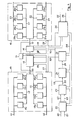
- FIG. 4 shows a device for converting an input sampling sequence into an output sampling sequence consisting of a single, single-stage digital filter 13, preferably designed as a transversal filter.
- Memories 14 and 15 are arranged on both sides of the filter 13.
- a multiplier 16 is also connected in series with the filter 13 and a bypass 17 in parallel with both.
- the memory 14 consists of two groups 18, 19 of memory units or registers 18a connected in parallel, b, c, d and 19a, b, 19c, 19d.
- One group 18 stores samples of a first, the other group 19 stores samples of a second channel.
- the memory 15 is also organized from groups 20, 21 of memory units 20a, 20b, 20c, 20d and 21a, 21b, 21c, 21d for two channels.
- a circuit comprising a time measuring circuit 22, a compensation circuit 23, a modulo circuit 24 and an interpolation circuit 25 is also provided.
- a controller 26 serves to control the functional sequences in the individual elements of the device.
- FIG. 5 partially shows the structure of the compensation circuit 23, with a compensation filter 27 and two addition elements 29 and 30 and white multipliers 31 and 32.
- This compensation circuit 23 has two inputs 62 and 63 and an output 33.
- FIG. 6 schematically shows the structure of the interpolation circuit 25.
- a counter 39 is connected upstream of a memory 40, which in turn is connected to two further memories 41 and 42.
- a subcircuit 43 and an inverter 44 are connected upstream of the memories 41 and 42.
- Lines 35, 36 and 37 form the outputs of the memories 41 and 42.
- the lines 35 and 36 open into a multiplier 70, the output 64 of which in turn opens into the adder 71 together with the line 37.
- Samples 3a, 3b, 3c etc. of an input sample sequence 1 reach the memory 14 via lines 45 and 46.
- Each of the incoming sample values of the input sample sequence 1 reaches one of the memory units 18, a, b, c, d or 19, a, b, c, d.
- These storage units each only record a single sample 3a, 3b, 3c etc. for a short time.
- the samples are then fed via lines 48, 49 and 50 to the filter 13, where they are processed, and leave the latter via line 47 as an output sample sequence 10.
- this output sample sequence 10 can be divided again into separate output sample sequences for 2 separate channels.
- the output scanning sequence 10 is fed via lines 51 and 52 to the storage units 20a, b, c, d and 21a, b, c, d and leaves them via lines 53 and 54.
- the control 26 is supplied with the input sampling frequency ⁇ 1 at the input 55 and the output sampling frequency w 2 at the input 56. It issues control commands to the memories 14 and 15 via the control bus 57 and 58. Within these memories 14 and 15, the control commands are forwarded to the two individual memory units 18, 19, 20, 21 in a manner known per se and therefore not shown here.
- the output samples 12a, 12b, 12c, etc. are precisely synchronized with the desired output sampling frequency. This means that the individual samples only pass through the storage units 20 and 21 and that the input samples remain in the storage units 18 and 19 until they are called up by the control commands and supplied to the filter 13. In this operating case, the memory 15 therefore has no actual function to be performed.
- the controller 26 synchronizes the activity of the filter 13 with the output scanning sequence 10.
- the input samples 3a, 3b, 3c etc. pass through lines 45 and 46 into memory 14, pass through them and then through filter 13.
- multiplier 16 the incoming output samples are multiplied by a ratio of the input and output sampling frequencies.
- Corresponding instructions are fed to the multiplier 16 via the control bus 73.
- the output samples 12a, 12b, 12c etc. then arrive via line 47 in the memory 15, where they are recorded by the individual memory units 20a, b, c, d and 21a, b, c, d.
- the controller 26 synchronizes the operation of the filter 13 to the input sample sequence 1.
- the input samples 3a, 3b, 3c etc. simply go through the storage units 18a, b, c, d and 19a, b, c, d and after the treatment in the filter 13 in the storage units 20a, b, c, d and 21 a, b, c, d of the memory 15 are stored. They remain there until the controller 26 issues output commands to the memory 15.
- the output samples 12a, b, c, etc. are then output in synchronism with the output sample sequence 10.
- the mode of operation of the filter 13 can be seen from FIGS. 1 to 3.
- the input sample sequence becomes 1 with additional samples 4a, 4b, 4c, etc. provided.
- 7 further samples are added between two samples 3a and 3b, 2. This results in a grid that is fine enough to be able to perform the setting of the filter 13 in this grid with the slightest errors in relation to an output sample.
- the output sampling sequence 10 is in relation to its output sampling frequency w2 and the phase position of its samples 12a, 12b. 12c etc. to be considered as given. We are looking for the signal amplitude of the samples 12, 12b, 12c etc.
- the digital filter 13 In order to process the input sample sequence 1, the digital filter 13 is now set on a raster with the sample values 4a, 4b etc. in such a way that the filter axis 8 (FIG. 2) in turn with each of the sample values 12a, 12b, 12c etc. of the output sample sequence 10 appears in the same phase as possible. In this phase position, the filter 13 generates a value for the signal amplitude of the sample in question. Here in FIGS. 1 to 3, this applies to a sample 12d.
- the phase position of the filter coefficients 7 does not match the phase position of the input samples 3a, 3b, 3c, etc.
- the result of such filtering would result in a signal amplitude of zero for the sample value 12d, which is certainly not correct.
- This error could be remedied by a filter with an infinite number of filter coefficients. However, this would also result in an infinitely high computing effort, which is practically unusable.
- our filter 13 has a very limited number of filter coefficients 7, for example their 6399, 3839, 6655 .. depending on the application of the device for radio, studio or radio and studio recordings.
- the filter order or the number of stored filter coefficients 7 is calculated as the product of the number of additional samples 4a, b, c, for example 2 7 and the number of input samples 3, z. B. 50.30.52 or 56 of the input sample sequence 1, which are used for the calculation of an output sample value, minus one.
- new filter coefficients must be obtained by interpolation.
- This can be done by linear interpolation between two support points or filter coefficients 7 or by quadratic interpolation between three filter coefficients 7.
- more filter coefficients 7 are taken into account for the higher order interpolation.
- the filter coefficients of the filter 13 can also be obtained for any values from a prototype function which is multiplicatively coupled to a window function. Only the constants of the relevant functions are saved. In each case, those function values are calculated that coincide with the input sample values.
- One such prototype function is called sin (nT) nT.
- the time measuring circuit is fed with the input sampling frequency 0 ) 1 via the input 60 and the output sampling frequency o 2 via the input 61.
- the construction of such a time measuring circuit 22 is known, for example, from European Patent Application No. 0 084 592.
- the timing circuit 22 calculates the ratio of the time differences between two samples 3a, b and 12a, b of the input and the
- This ratio is fed to the compensation circuit 23 as a 16 bit number via line 62 and as an 8 bit number via line 63.
- the number that is passed via line 62 is averaged with a larger number of previous values, as is known from EP-0 084 592, while the number passed via line 63 corresponds to the value measured with 2 8 counts.
- the values of the lines 62 and 63 are each multiplied by 28 in multipliers 31 and 32. This means that the adder 29 is supplied with 16 bit numbers and the adder 30 with 24 bit numbers. Before multiplication in multiplier 3, the 16-bit numbers from line 62 are fed to adder 29, where they are mixed with the values from line 63 multiplied to a 16-bit number.
- the mixed value from the lines 62 and 63 is again averaged over a number of cycles in the compensation filter 27, just as in the time measurement circuit 22, and is fed to the adder 30, where this value is averaged with the original averaged value from the time measurement circuit 22.
- a faster response of the circuit can be brought about in the event of changes in the sampling rates, since there is no need to wait until a sufficiently large number of values has influenced the averaging in the time measuring circuit 22.
- a few new values can have a strong influence on the time measurement after the mixing in the adder 29.
- the compensated ratios of the time differences of the modulo forming circuit 24 are supplied from the compensation circuit 23. This consists of a series connection of one register with one
- the filter axis 8 of the digital filter 13 with the filter coefficients 7 successively on each of the output samples 12a, b, c, d, etc. is set.
- the filter axis 8 of the digital filter 13 with the filter coefficients 7 successively on each of the output samples 12a, b, c, d, etc. is set.
- the output sample 12d for example, 56 input samples are successively multiplied by corresponding filter coefficients and the products are added up. This is done in the filter 13 in a manner known per se.
- the interpolation circuit 25, determines which filter coefficients 9, 9 ', etc. are used for each of these 56 input samples 3a, 3b, etc.
- the controller 26 starts the counter 39 (FIG. 6) for each of these cycles, in which these 56 multiplications are carried out, for example, via the control bus 38.
- the latter now continuously outputs v values (for example from 1 to 56) which act as addresses for the input samples 3a, b, c etc. stored in a memory 91 belonging to the filter 13.
- v values for example from 1 to 56
- m values are also input into a subcircuit 43 via line 34 from the modulo-forming circuit 24.
- These m-values are data words which comprise 15 bits and determine the point in time of the output sample value (for example 12d) which is essential for the relevant clock in relation to the input sample value grid.
- the first 7 bits of the data word m indicate a value s for the input samples 3a, b, c, etc., which denotes the closest filter coefficients, the last 8 bits indicate the distance a between the next filter coefficient 8 and the input sample 3h.
- the interpolation formula for filter coefficients is C;
- D j denotes the difference between two adjacent filter coefficients.
- the v-values are fed to the memory 40 and then reach the memories 41 and 42. After the subcircuit 43, the a-values reach the memory 42 via line 65. The s-values reach the memory 41 via the inverter 44. In this are all filter coefficients C i and all differences D; saved.
- the incoming i-values, which have been composed in memory 44 from the s-values and the v-values, are thus considered as addresses for the relevant C i and Di values, which leave memory 41 via lines 36 and 37 .
- the Di values are multiplied in the multiplier 70 by the a values from line 35 and then fed via line 64 to the adder 71, where they are combined with the C i value from line 37.
- a completely interpolated filter coefficient C i, a leaves the adder 71 via line 59.
- the filter coefficients 7 are symmetrical with respect to the filter axis 8, only the first half thereof has to be saved. Therefore, the second half of the filter coefficients is recoded in the memory 40 and the s values for the second half of the filter coefficients are inverted in the inverter 44. The v-values e.g. B. from the 56th value are counted down and the a values are subtracted from its maximum value.
- the output sampling sequence is provided with additional sampling values assumed to be zero.
- the operation of the filter 13 and also the processing of the filter coefficients is synchronized with the input sampling sequence. Accordingly, the v-values indicate addresses for products of input samples and filter coefficients, and the m-values indicate the point in time of the input sample relevant to the relevant clock in relation to the output sample raster.
- the controller 26 is connected to the line 33 via a line 67.
- Line 33 transmits data relating the ratio of time differences ö and ö; specify between successive sample rates of the input or output sample sequence. From this data it can be derived when the device changes from one operating case to the other with changing sampling frequencies. This is continuously recorded by the controller 26.
- input sampling values stored in the memory 14 can be used directly as long as the input sampling frequency approximately corresponds to the output sampling frequency. These are fed directly to the memory 15 via the bypass 17.
- This operating state lasts 56 clocks if 12, 56 input samples are used to form an output sample.
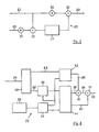
- a possible embodiment for a filter 13 can be seen from FIG.
- the structure of the filter 13 shown consists of a combination of the 1st and 2nd canonical structures.
- the filter has a certain number of multipliers 80a, 80b, 80c, 80d etc.
- the number of these multipliers 80 corresponds to the number of input samples 3a, 3b, 3c, etc. (e.g. 56) which are used to calculate an output sample 12d.
- the number of time delay circuits or registers 81 a, b, c and 82a, b, c, which are each arranged between two multipliers 80, is reduced accordingly by one.
- Switches 83a, b, c are connected in parallel with the registers 81a, b, c.
- Adding elements 84a, b, c are arranged in series with the registers 82a, b, c etc.
- a summing circuit 85 is also arranged in parallel with the multipliers 80.
- Each multiplier 80a, b, c also has an input 88a, b, c, d for the filter coefficients.
- a switch 89 serves to switch the filter 13 to the operating states a) and b).
- a first sample value arriving at input 90 is fed on the one hand to register 81a, where it remains stored until the second sample value arrives at input 90 and on the other hand fed to multiplier 80a in which the sample value is multiplied by a filter coefficient and fed to summing circuit 35.
- the second sample arrives at input 90, it is in turn fed to multiplier 80a and register 81a, which now supplies the first sample to multiplier 80b, etc.
- summing circuit 85 also outputs an output sample via the output 87, which consists of a sum of four successive input samples, each multiplied by a filter coefficient. In our filter 13 these are not four but fifty-six consecutive samples which are summed up in a filter with 56 multipliers and 55 registers etc.
- the first product from the multiplier 80a is entered into the register 82a.
- the products reach the adders 84a, b, c from the multipliers 80b, 80c and 80d.
- There the product from the multiplier 80b is summed up with a product from the register 82a.
- a third product from the multiplier 80c is added to this sum, which is now stored in the register 82b, in the adder 84b, etc.
- a sum is output via the switch 89, which consists of four successive input samples, each multiplied by a filter coefficient.
- the filter according to FIG. 7 can also be designed. It comprises a memory 91, a single multiplier 92 with an input 93 for filter coefficients, an adder 94 with an output 95 and an input 96 and 97, a further memory 98 being connected between the output 95 and the input 97.
- the memories 91 and 98 also have inputs 99 and 100, known per se, for memory addresses.
- the adder 94 forms an accumulator circuit 101 with the memory 98.
- a number of successive samples (eg 56) are read into corresponding memory locations in the memory 91.
- Read sample values are fed to the multiplier 92, multiplied there by a filter coefficient and then fed to the adder 94.
- memory 98 only one memory location is used for a single value.
- all fifty-six samples are read out of the memory 91 once and fed to the multiplier and the adder 94, where these values are continuously accumulated.
- An intermediate result of the accumulation is stored in the memory 98. Once all the samples of the memory 91 have been read out, the entire contents of the memory 91 are shifted by one sample and the process mentioned begins again.
- ⁇ 1 > w 2 only one memory location is used for a single sample value in the memory 91, while all memory locations for (e.g. 56) several values are used in the memory 98.
- a certain sample value is made out so many times in the same cycle taken from the memory 91 and multiplied by as many filter coefficients in the multiplier 92 as values are stored in the memory 98 (e.g. 56 times).
- Each value is extracted once from the cycle 98 and added in the adder 94 with the product from the multiplier 92 and read back into the old memory location.
- the oldest value is no longer read from the memory 91 after the addition, but is read out via the output 95.
- a new sample value is read into the memory 98 and the entire memory content is shifted by one memory location or a value and these processes start again.
- a single multiplier is thus operated in the filter using the time-division multiplex method. Switching from operating state a) to b) is done here by a different assignment of the memory addresses.
- the addresses which are created per cycle in the operating case a) are stored in the memory 100 in the operating case b).
Abstract
Description
Die Erfindung betrifft ein verfahren und eine Vorrichtung zum Umsetzen der Abtastwerte einer Eingangsabtastfolge, die mit einer Eingangsabtastfrequenz auftreten, in Abtastwerte einer Ausgangsabtastfolge, die mit einer Ausgangsabtastfrequenz auftreten derart, dass die Eingangsabtastfolge und die Ausgangsabtastfolge Frequenzspektren aufweisen, die in einem Frequenzbereich amplitudenmässig im wesentlichen identisch sind, der sich von der Frequenz Null bis zur Hälfte der niedrigeren der beiden Abtastfrequenzen erstreckt.The invention relates to a method and a device for converting the samples of an input sample sequence that occur with an input sample frequency into samples of an output sample sequence that occur with an output sample frequency such that the input sample sequence and the output sample sequence have frequency spectra that are essentially identical in amplitude in a frequency range are, which extends from the frequency zero to half of the lower of the two sampling frequencies.
Ein solches Verfahren und eine solche Vorrichtung sind aus der europäischen Patentanmeldung EP-A-0 052 847 bereits bekannt. Bei diesem Verfahren und bei dieser Vorrichtung geschieht die Umsetzung der Eingangsabtastfolge in die Ausgangsabtastfolge durch mehrmaliges digitales Filtern der Eingangsabtastwerte in einem mehrstufigen digitalen Filter. Dabei wird die Eingangsabtastfolge in mehreren Schritten in die Ausgangsabtastfolge uebergefuehrt. Dieser vorgang wird gesteuert durch die momentane zeitliche Differenz zwischen dem Eingangs- und dem Ausgangsabtastzeitpunkt. Diese Differenz wird zur Berechnung eines momentanen Filterkoeffizientensatzes verwendet. Ein wichtiger Teil dieser Vorrichtung ist deshalb zur Ermittlung dieser zeitlichen Differenz vorgesehen.Such a method and such a device are already known from European patent application EP-A-0 052 847. In this method and in this device, the conversion of the input sample sequence into the output sample sequence is carried out by digitally filtering the input sample values several times in a multi-stage digital filter. The input scan sequence is converted into the output scan sequence in several steps. This process is controlled by the instantaneous time difference between the input and the output sampling time. This difference is used to calculate a current set of filter coefficients. An important part of this device is therefore provided to determine this time difference.
Bisher bekannte Vorrichtungen zur Ermittlung der zeitlichen Differenz zwischen Eingangs- und Ausgangsabtastzeitpunkten können bei rasch wechselnden Eingangs- und Ausgangsabtastfrequenzen nicht folgen. Dies einerseits weil der Zwischenspeicher bei einem mehrstufigen Abtastratenwandler klein ist. Andererseits fuehrt die Verarbeitung von zeitlich variierenden Abtastfrequenzen zu Zeitdifferenzen zwischen den momentan effektiv vorhandenen Abtastwerten und den errechneten Zeitdifferenzen zwischen den betreffenden Ein-und Ausgangsabtastwerten. Deshalb kann bei rasch wechselnden Abtastfrequenzen der Zwischenspeicher nicht mehr genuegend Abtastwerte Zwischenspeichern, was bedeutet, dass die Vorrichtung ihre Funktion nicht mehr erfuellen kann. Ein weiterer Nachteil des mehrstufigen Abtastratenwandlers ist darin zu sehen, dass bei kontinuierlich wechselnden Eingangs- und Ausgangsabtastfrequenzen, wobei sowohl die Eingangs als auch die Ausgangsabtastfrequenz abwechselnd höhere Werte annehmen kann, die Arbeitsfolge der einzelnen Stufen des mehrstufigen digitalen Filters vertauscht werden muss, was nicht ohne Arbeitsunterbruch erfolgen kann.Previously known devices for determining the time difference between input and output sampling instants cannot follow rapidly changing input and output sampling frequencies. On the one hand, this is because the buffer in a multi-stage sample rate converter is small. On the other hand, the processing of time-varying sampling frequencies leads to time differences between the actually effective samples and the calculated time differences between the relevant input and output samples. Therefore, in the case of rapidly changing sampling frequencies, the buffer store can no longer buffer enough sample values, which means that the device can no longer perform its function. Another disadvantage of the multi-stage sampling rate converter is that with continuously changing input and output sampling frequencies, where both the input and the output sampling frequency can alternately take on higher values, the working sequence of the individual stages of the multi-stage digital filter must be interchanged, which is not without Work can be interrupted.
Die Erfindung wie sie in den Ansprüchen gekennzeichnet ist, löst die Aufgabe ein Verfahren und eine Vorrichtung zu schaffen, die zur Umsetzung wechselnder Eingangs- und Ausgangsabtastraten geeignet sind und die mitThe invention as characterized in the claims solves the problem of creating a method and a device which are suitable for implementing changing input and output sampling rates and which
einem begrenzten Rechen- und Speicheraufwand auskommen.a limited amount of computing and memory.
Die durch die Erfindung erreichten Vorteile sind im wesentlichen darin zu sehen, dass Abtastfolgen verarbeitet werden können, die kontinuierlich varierende Abtastfrequenzen aufweisen, und zwar insbesondere auch z. B. wenn die eine Abtastfrequenz die ursprünglich grösser oder kleiner war als die andere Abtastfrequenz sich so verändert, dass sie nun kleiner oder grösser als die andere Abtastfrequenz wird. Durch diese Vorrichtung kann ein Signal mit einer zeitvariablen Abtastrate in ein Signal mit einer beliebigen anderen zeitvariablen oder konstanten Abtastrate umgewandelt werden. Es können Filter zur Anwendung vorgesehen werden, deren Filterordnung kleiner ist, als die totale Filterordnung eines mehrstufigen Filters. Dies verringert den Aufwand für die Koeffizientenspeicherung und die Berechnung der neuen Abtastwerte.The advantages achieved by the invention are essentially to be seen in the fact that scanning sequences can be processed which have continuously varying scanning frequencies, in particular also e.g. B. if the one sampling frequency that was originally larger or smaller than the other sampling frequency changes so that it is now smaller or larger than the other sampling frequency. With this device, a signal with a time-variable sampling rate can be converted into a signal with any other time-variable or constant sampling rate. Filters can be provided for the application, the filter order of which is smaller than the total filter order of a multi-stage filter. This reduces the effort for storing the coefficients and calculating the new samples.
Im folgenden wird die Erfindung anhand von einen Ausführungsweg darstellenden Zeichnungen näher erläutert. Es zeigen:
- Figur 1 eine Eingangsabtastfolge eines Signales,
Figur 2 die Fiterkoeffizienten eines digitalen Filters,Figur 3 eine Ausgangsabtastfolge des Signals,- Figur 4 eine Vorrichtung zur Wandlung von Abtastfolgen in schematischer Darstellung,
- Figur 5 eine Schaltung zur Kompensation von Zeitdifferenzen,
Figur 6 eine Interpolationsschaltung,- Figur 7 und 8 je ein Filter.
- 1 shows an input sampling sequence of a signal,
- FIG. 2 shows the fit coefficients of a digital filter,
- FIG. 3 shows an output sample sequence of the signal,
- FIG. 4 shows a device for converting scan sequences in a schematic illustration,
- FIG. 5 shows a circuit for compensating for time differences,
- FIG. 6 shows an interpolation circuit,
- Figures 7 and 8 each have a filter.
In Figur 1 ist eine Eingangsabtastfolge 1 über einer Zeitachse 2 aufgetragen. Die einzelnen Abtastwerte 3a, 3b. 3c usw. folgen einander in Zeitabständen A tj. Auf der Zeitachse 2 sind weitere Abtastwerte 4a, 4b. 4c usw. ersichtlich, die sich in Zeitabständen 5-folgen, die wesentlich kleiner sind als Δ tj. Die Signalamplitude dieser weiteren Abtastwerte sei null. Eine Eingangsabtastfrequenz ω1 ergibt sich dementsprechend aus dem Kehrwert von Atl.In Figure 1, an input scan sequence 1 is plotted over a
In Figur 2 sind über einer Zeitachse 6 Werte von Filterkoeffizienten 7 eines digitalen und insbesondere transversalen Filters aufgetragen. Mit 8 ist der als Filterachse zu zählende Filterkoeffizient bezeichnet. Ferner sind Werte von Koeffizienten 9,9', die aus einer Interpolation gewonnen werden eingetragen.In FIG. 2, values of filter coefficients 7 of a digital and in particular transverse filter are plotted over a
Figur 3 zeigt eine Ausgangsabtastfolge 10 über einer Zeitachse 11 aufgetragen mit Abtastwerten 12a, 12b, 12c usw., die einander in Zeitabständen At2 folgen. Eine Ausgangsabtastfrequenz w2 ergibt sich dementsprechend aus dem Kehrwert von At2.FIG. 3 shows an
Figur 4 zeigt eine Vorrichtung zur Umsetzung einer Eingangsabtastfolge in eine Ausgangsabtastfolge bestehend aus einem einzigen, einstufigen digitalen Filter 13, vorzugsweise als Transversalfilter ausgebildet. Beideseits des Filters 13 sind Speicher 14 und 15 angeordnet Mit dem Filter 13 in Serie geschaltet ist ferner ein Multiplikator 16 und parallel zu beiden ein Bypass 17. Der Speicher 14 besteht aus je zwei Gruppen 18, 19 von parallel geschalteten Speichereinheiten bzw. Registern 18a, b, c, d und 19a, b, 19c, 19d. Die eine Gruppe 18 speichert Abtastwerte eines ersten, die andere Gruppe 19 speichert die Abtastwerte eines zweiten Kanals. Genauso ist auch der Speicher 15 aus Gruppen 20, 21 von Speichereinheiten 20a, 20b, 20c, 20d und 21 a, 21 b, 21 c, 21 d für zwei Kanäle organisiert.FIG. 4 shows a device for converting an input sampling sequence into an output sampling sequence consisting of a single, single-stage
Zur Aufbereitung der Filterkoeffizienten für das Filter 13 ist ferner eine Schaltung bestehend aus einer Zeitmeßschaltung 22, einer Kompensationsschaltung 23, einer Modulobildungsschaltung 24 und einer Interpolationsschaltung 25, vorgesehen. Eine Steuerung 26 dient der Steuerung der Funktionsabläufe in den einzelnen Elementen der Vorrichtung.For the preparation of the filter coefficients for the
Figur 5 zeigt teilweise den Aufbau der Kompensationsschaltung 23, mit einem Kompensationsfilter 27 und zwei Additionsgliedern 29 und 30 und wei Multiplikatoren 31 und 32.FIG. 5 partially shows the structure of the
Diese Kompensationsschaltung 23 weist zwei Eingänge 62 und 63 sowie einen Ausgang 33 auf.This
Figur 6 zeigt schematisch den Aufbau der Interpolationsschaltung 25. Darin ist ein Zähler 39 einem Speicher 40 vorgeschaltet, welcher wiederum mit zwei weiteren Speichern 41 und 42 verbunden ist. Eine Teilschaltung 43 sowie ein Inverter 44 sind den Speichern 41 und 42 vorgeschaltet. Leitungen 35, 36 und 37 bilden die Ausgänge der Speicher 41 und 42. Die Leitungen 35 und 36 münden in einen Multiplikator 70, dessen Ausgang 64 wiederum zusammen mit der Leitung 37 in das Additionsglied 71 mündet.FIG. 6 schematically shows the structure of the
Für die Beschreibung der Wirkungsweise des Verfahrens bzw. der Vorrichtung sind zwei verschiedene Betriebszustände zu unterscheiden:
- a) Die Ausgangsabtastrate ist höher als die Eingangsabtastrate o)2 > ω1
- b) Die Ausgangsabtastrate ist kleiner als die Eingangsabtastrate o2 > ω1
- a) The output sampling rate is higher than the input sampling rate o) 2> ω 1
- b) The output sampling rate is lower than the input sampling rate o 2 > ω 1
Dabei gelangen Abtastwerte 3a, 3b, 3c usw. einer Eingangsabtastfolge 1 beispielsweise von zwei getrennten Kanälen eines Audio-Wiedergabegerätes über Leitungen 45 und 46 in den Speicher 14. Jeder der eintreffenden Abtastwerte der Eingangsabtastfolge 1 gelangt in eine der Speichereinheiten 18, a, b, c, d oder 19, a, b, c, d. Dabei nehmen diese Speichereinheiten jeweils nur einen einzigen Abtastwert 3a, 3b, 3c usw. für kurze Zeit auf. Wie später noch genauer beschrieben wird, werden die Abtastwerte anschliessend über Leitungen 48,49 und 50 dem Filter 13 zugeleitet, wo sie verarbeitet werden und verlassen diesen über Leitung 47 als Ausgangsabtastfolge 10. Im Speicher 15 kann diese Ausgangsabtastfolge 10 wieder aufgeteilt werden in getrennte Ausgangsabtastfolgen für 2 getrennte Kanäle. Dazu wird die Ausgangsabtastfolge 10 über Leitungen 51 und 52 den Speichereinheiten 20a, b, c, d und 21a, b, c, d zugeleitet und verlässt diese über Leitungen 53 und 54.
Der Steuerung 26 wird am Eingang 55 die Eingangsabtastfrequenz ω1, und am Eingang 56 die Ausgangsabtastfrequenz w2 zugeleitet. Über den Steuerbus 57 und 58 gibt sie Steuerbefehle an die Speicher 14 und 15 ab. Innerhalb dieser Speicher 14 und 15 werden die Steuerbefehle in an sich bekannter und deshalb hier nicht näher dagestellter Weise an die beiden einzelnen Speichereinheiten 18, 19, 20, 21 weitergeleitet. Dabei werden die Ausgangsabtastwerte 12a, 12b, 12c usw. genau mit der gewünschten Ausgangsabtastfrequenz synchronisiert. Das bedeutet, dass die einzelnen Abtastwerte die Speichereinheiten 20 und 21 nur durchlaufen und dass die Eingangsabtastwerte in den Speichereinheiten 18 und 19 solange verweilen, bis sie durch die Steuerbefehle abgerufen und dem Filter 13 zugeführt werden. In diesem Betriebsfall hat der Speicher 15 somit keine eigentliche Funktion zu erfüllen Die Steuerung 26 synchronisiert die Tätigkeit des Filters 13 auf die Ausgangsabtastfolge 10.The
Die Eingangsabtastwerte 3a, 3b, 3c usw. gelangen wiederum über die Leitun gen 45 und 46 in den Speicher 14, durchlaufen diesen sowie anschliessend das Filter 13. Im Multiplikator 16 werden die eintreffenden Ausgangsabtastwerte mit einem Verhältniswert aus der Eingangs- und Ausgangsabtastfrequenz multipliziert. Entsprechende Instruktionen werden dem Multiplikator 16 über den Steuerbus 73 zugeleitet. Die Ausgangsabtastwerte 12a, 12b, 12c usw. gelangen dann über Leitung 47 in den Speicher 15, wo sie durch die einzelnen Speichereinheiten 20a, b, c, d und 21 a, b, c, d aufgenommen werden.The
In diesem Fall synchronisiert die Steuerung 26 die Tätigkeit des Filters 13 auf die Eingangsabtastfolge 1. Das bedeutet, dass die Eingangsabtastwerte 3a, 3b, 3c usw. die Speichereinheiten 18a, b, c, d und 19a, b, c, d einfach durchlaufen und nach der Behandlung im Filter 13 in den Speichereinheiten 20a, b, c, d und 21 a, b, c, d des Speichers 15 gespeichert werden. Dort bleiben sie, bis die Steuerung 26 Ausgabebefehle an den Speicher 15 erteilt. Die Ausgabe der Ausgangsabtastwerte 12a, b, c usw. erfolgt dann synchron zur Ausgangsabtastfolge 10.In this case, the
Am Beispiel des Falles a) soll nun auch die Wirkungsweise des Filters 13 sowie der Schaltung 22 bis 25 zur Aufbereitung der Filterkoeffizienten 9, 9' erläutert werden.Using the example of case a), the mode of operation of the
Die Wirkungsweise des Filters 13 geht aus den Figuren 1 bis 3 hervor. Zuerst wird die Eingangsabtastfolge 1 mit weiteren Abtastwerten 4a, 4b, 4c usw. versehen. Beispielsweise werden zwischen zwei Abtastwerten 3a und 3b, 27 weitere Abtastwerte beigegeben. Dies ergibt einen Raster, der fein genug ist, um die Einstellung des Filters 13 in diesem Raster mit geringsten Fehlern in bezug auf einen Ausgangsabtastwert vollziehen zu können.The mode of operation of the
Die Ausgangsabtastfolge 10 ist in bezug auf ihre Ausgangsabtastfrequenz w2 und die Phasenlage ihrer Abtastwerte 12a, 12b. 12c usw. als gegeben zu betrachten. Gesucht ist die Signalamplitude der Abtastwerte 12, 12b, 12c usw.The
Zur Verarbeitung der Eingangsabtastfolge 1 wird nun das digitale Filter 13 auf einem Raster mit den Abtastwerten 4a, 4b usw. so eingestellt, dass die Filterachse 8 (Fig. 2) der Reihe nach mit jedem der Abtastwerte 12a, 12b, 12c usw. der Ausgangsabtastfolge 10 in möglichst gleicher Phasenlage erscheint. In dieser Phasenlage erzeugt das Filter 13 einen Wert für die Signalamplitude des betreffenden Abtastwertes. Hier in den Figuren 1 bis 3 trifft dies für einen Abtastwert 12d zu.In order to process the input sample sequence 1, the
Wie aus den Figuren 1 bis 3 hervorgeht, stimmt die Phasenlage der Filterkoeffizienten 7 nicht mit der Phasenlage der Eingangsabtastwerte 3a, 3b, 3c, usw. überein. Das Resultat einer solchen Filterung er gäbe für den Abtastwert 12d eine Signalamplitude von null, was sicher nicht richtig ist. Dieser Fehler könnte durch ein Filter mit einer unendlich grossen Zahl von Filterkoeffizienten behoben werden. Dies ergäbe aber auch einen unendlich hohen Rechenaufwand, was praktisch nicht brauchbar ist.As can be seen from FIGS. 1 to 3, the phase position of the filter coefficients 7 does not match the phase position of the
Im Gegensatz dazu weist unser Filter 13 eine sehr beschränkte Anzahl von Filterkoeffizienten 7 auf, beispielsweise deren 6399, 3839, 6655.. je nach Anwendung der Vorrichtung für Rundfunk, Studio oder Rundfunk und Studio-Aufnahmen. Dabei berechnet sich die Filterordnung bzw. die Anzahl der gespeicherten Filterkoeffizienten 7 als das Produkt aus der Anzahl der zusätzlichen Abtastwerte 4a, b, c, beispielsweise 27 und der Anzahl der Eingangsabtastwerte 3, z. B. 50.30.52 oder 56 der Eingangsabtastfolge 1, die für die Berechnung eines Ausgangsabtastwertes herangezogen werden, minus eins.In contrast, our
Für alle Abtastwerte der Eingangsabtastfolge 1, die nicht in Phase sind mit Filterkoeffizienten 7 des auf einen bestimmten Abtastwert der Ausgangsabtastfolge 10 eingestellten Filters 13, müssen neue Filterkoeffizienten durch Interpolation gewonnen werden. Beispielsweise gilt dies in Figur 1 und 2 für die Abtastwerte 3g und 3h, für die neue Filterkoeffizienten 9 und 9' errechnet werden müssen. Dies kann durch lineare Interpolation zwischen zwei Stützstellen bzw. Filterkoeffizienten 7 oder durch quadratische Interpolation zwischen drei Filterkoeffizienten 7 geschehen. Für die Interpolation höherer Ordnung werden entsprechend mehr Filterkoeffizienten 7 berücksichtigt.For all samples of the input sample sequence 1 that are not in phase with filter coefficients 7 of the
Anstelle einer Interpolation zwischen gespeicherten Filterkoeffizienten können die Filterkoeffizienten des Filters 13 auch für beliebige Werte aus einer Prototyp-Funktion, welche mit einer Fenster-Funktion multiplikativ gekoppelt ist, gewonnen werden. Gespeichert sind lediglich die Konstanten der betreffenden Funktionen. Berechnet werden jeweils diejenigen Funktionswerte, die zeitlich mit den Eingangsabtastwerten zusammenfallen. Eine mögliche solche Prototyp-Funktion heisst sin(nT) nT.Instead of an interpolation between stored filter coefficients, the filter coefficients of the
Diese interpolierten Filterkoeffizienten werden für den Filter 13 laufend in den Schaltungen 22 bis 25 berechnet und dem Filter 13 über Leitung 59 zugeführt. Das Filter 13 an sich arbeitet aber wieder in bekannter Weise.These interpolated filter coefficients are continuously calculated for the
Zur Aufbereitung der Filterkoeffizienten 7 wird der Zeitmeßschaltung über den Eingang 60 die Eingangsabtastfrequenz 0)1 und über den Eingang 61 die Ausgangsabtastfrequenz o2 zugeleitet. Der Aufbau einer solchen Zeitmeßschaltung 22 ist beispielsweise aus der Europäischen Patentanmeldung Nr. 0 084 592 bekannt. Die Zeitmeßschaltung 22 berechnet das Verhältnis der Zeitdifferenzen zwischen zwei Abtastwerten 3a, b und 12a, b der Eingangs- und derTo prepare the filter coefficients 7, the time measuring circuit is fed with the input sampling frequency 0 ) 1 via the
Ausgangsabtastfolge 1 und 10, öi; für den Fall b) und Δt2 Δt1 für den Fall a).
Dieses Verhältnis wird als 16 Bit-Zahl über Leitung 62 und als 8 Bit-Zahl über Leitung 63 der Kompensationsschaltung 23 zugeführt. Dabei ist diejenige Zahl die über Leitung 62 geleitet wird mit einer grösseren Anzahl vorausgehender Werte gemittelt, wie aus EP-0 084 592 bekannt, während die über die Leitung 63 geleitete Zahl dem mit 28 Zählimpulsen gemessenen Wert entspricht. In der Kompensationsschaltung 23 werden die Werte der Leitungen 62 und 63 jeweils mit 28 multipliziert in Multiplikatoren 31 und 32. Das bedeutet, dass dem Additionsglied 29 16 Bit Zahlen und dem Additionsglied 30 24 Bit Zahlen zugeführt werden. Vor der Multiplikation im Multiplikator 3, werden die 16 Bit Zahlen aus Leitung 62 dem Additionsglied 29 zugeführt, wo sie mit den auf eine 16 Bit-Zahl multiplizierten Werten aus Leitung 63 gemischt werden.This ratio is fed to the
Der Mischwert aus den Leitungen 62 und 63 wird im Kompensationsfilter 27 wiederum genau wie in der Zeitmeßschaltung 22 über mehrere Takte gemittelt und dem Additionsglied 30 zugeführt, wo dieser Wert mit dem ursprünglichen gemittelten Wert aus der Zeitmeßschaltung 22 gemittelt wird. Auf diese Weise kann bei Änderungen der Abtastraten eine schnellere Reaktion der Schaltung herbeigeführt werden, denn es muss nicht abgewartet werden, bis eine genügend grosse Anzahl Werte die Mittelwertbildung in der Zeitmeßschaltung 22 beeinflusst hat. Schon wenige neue Werte können die Zeitmessung nach der Mischung im Additionsglied 29 stark beeinflussen.The mixed value from the
Von der Kompensationsschaltung 23 werden die kompensierten Verhältnisse der Zeitdifferenzen der Modulobildungsschaltung 24 zugeführt. Diese besteht aus einer Serieschaltung von einem Register mit einemThe compensated ratios of the time differences of the
Speicherplatz und einer Additionsstufe, wobei nach dem Register eine Rückführung auf die vorausgehende Additionsstufe angeordnet ist. In dieser Modulobildungsschaltung 24 werden zwei nacheinander folgende Werte gemischt und anschliessend an die Interpolationsschaltung 25 abgegeben.Storage space and an addition level, with a return to the previous addition level being arranged after the register. In this
In Erläuterung der Arbeitsweise der Interpolationsschaltung 25 ist nochmals in Erinnerung zu rufen, dass in dem vorliegenden Betriebsfall a) , wo ω2 > ω1 ist, die Filterachse 8 des digitalen Filters 13 mit den Filterkoeffizienten 7 nacheinander auf jeden der Ausgangsabtastwerte 12a , b , c, d usw. eingestellt wird. Zur Berechnung beispielsweise des Ausgangsabtastwertes 12d werden beispielsweise 56 Eingangsabtastwerte nacheinander mit entsprechenden Filterkoeffizienten multipliziert und die Produkte aufsummiert. Dies geschieht im Filter 13 auf an sich bekannte Weise. Welche Filterkoeffizienten 9, 9' usw. aber für jeden dieser 56 Eingangsabtastwerte 3a, 3b usw. zur Anwendung gelangen, bestimmt beispielsweise die Interpolationsschaltung 25.In explanation of the operation of the
Zu diesem Zweck startet die Steuerung 26 für jeden dieser Takte, in denen beispielsweise diese 56 Multiplikationen durchgeführt werden, über den Steuerbus 38 den Zähler 39 (Fig. 6). Dieser gibt nun laufend v-Werte (z. B von 1 bis 56) aus, die als Adressen für die in einem Speicher 91, der zum Filter 13 gehört, gespeicherten Eingangsabtastwerte 3a,b, c usw. wirken. Für jeden dieser Takte werden zudem uber Leitung 34 aus der Modulobildungsschaltung 24 sogenannte m-Werte in eine Teilschaltung 43 eingegeben. Diese m-Werte sind Datenwörter die 15 Bit umfassen und den Zeitpunkt des für den betreffenden Takt wesentlichen Ausgangsabtastwertes (z. B. 12d) in bezug auf den Eingangsabtastwertraster bestimmen.For this purpose, the
Die ersten 7-Bit des Datenwortes m geben für die Eingangsabtastwerte 3a, b, c usw. einen Wert s an, der die nächstgelegenen Filterkoeffizienten bezeichnet, die letzten 8-Bit geben den Abstand a zwischen dem nächstfolgenden Filterkoeffizienten 8 und dem Eingangsabtastwert 3h an. Somit gilt als Interpolationsformel für Filterkoeffizienten C;The first 7 bits of the data word m indicate a value s for the input samples 3a, b, c, etc., which denotes the closest filter coefficients, the last 8 bits indicate the distance a between the next filter coefficient 8 and the
![]()
![]()
![]()
![]()
![]()
![]()
Die v-Werte werden dem Speicher 40 zugeführt und gelangen anschliessend in die Speicher 41 und 42. Nach der Teilschaltung 43 gelangen die a-Werte über Leitung 65 in den Speicher 42. Die s-Werte gelangen über den Inverter 44 in den Speicher 41. In diesem sind alle Filterkoeffizienten Ci und alle Differenzen D; gespeichert. Die eintreffenden i-Werte, die im Speicher 44 aus den s-Werten und den v-Werten zusammengesetzt worden sind, gelten somit als Adressen für die betreffenden Ci- und Di-Werte, die den Speicher 41 über die Leitungen 36 und 37 verlassen. Die Di-Werte werden im Multiplikator 70 mit den a-Werten aus Leitung 35 multipliziert und anschliessend über Leitung 64 dem Additionsglied 71 zugeführt, wo sie mit dem Ci-Wert aus Leitung 37 kombiniert werden. Ein fertig interpolierter Filterkoeffizient Ci,a, verlässt das Additionsglied 71 über Leitung 59.The v-values are fed to the
Da die Filterkoeffizienten 7 bezüglich der Filterachse 8 symmetrisch sind, ist nur deren erste Hälfte zu speichern. Deshalb wird im Speicher 40 die zweite Hälfte der Filterkoeffizienten umkodiert und im Inverter 44 die s-Werte für die zweite Hälfte der Filterkoeffizienten invertiert. Die v-Werte z. B. vom 56-sten Wert werden zurückgezählt und die a-Werte von dessen Maximalwert subtrahiert.Since the filter coefficients 7 are symmetrical with respect to the filter axis 8, only the first half thereof has to be saved. Therefore, the second half of the filter coefficients is recoded in the
Im Betriebsfall b) in welchem die Ausgangsabtastrate kleiner ist als die Eingangsabtastrate, wird die Ausgangsabtastfolge mit zusätzlichen, als nullwertig angenommenen Abtastwerten versehen. Die Tätigkeit des Filters 13 und auch die Aufbereitung der Filterkoeffizienten ist auf die Eingangsabtastfolge synchronisiert. Dementsprechend geben die v-Werte Adressen für Produkte aus Eingangsabtastwerten und Filterkoeffizienten, die m-Werte den Zeitpunkt des für den betreffenden Takt wesentlichen Eingangsabtastwertes in bezug auf den Ausgangsabtastraster, an.In operating case b), in which the output sampling rate is lower than the input sampling rate, the output sampling sequence is provided with additional sampling values assumed to be zero. The operation of the
Um das Filter 13 und die Schaltung zur Aufbereitung der Filterkoeffizienten vom Betriebsfall a) auf den Betriebsfall b) umschalten zu können, ist die Steuerung 26 über eine Leitung 67, mit der Leitung 33 verbunden. Die Leitung 33 überträgt Daten, die das Verhältnis von Zeitdifferenzen ö bzw. ö; zwischen aufeinanderfolgenden Abtastraten der Eingangs- bzw. der Ausgangsabtastfolge angeben. Aus diesen Daten kann abgeleitet werden, wann bei sich ändernden Abtastfrequenzen die Vorrichtung vom einen Betriebsfall in den anderen wechselt. Dies wird von der Steuerung 26 laufend erfasst. Beim Übergang von einer höheren Ausgangsabtastfrequenz als die-Eingangsabtastfrequenz, können als Ausgangsabtastwerte im Speicher 14 gespeicherte Eingangsabtastwerte direkt verwendet werden, solange die Eingangsabtastfrequenz ungefähr der Ausgangsabstfrequenz entspricht. Diese werden über den Bypass 17 direkt dem Speicher 15 zugeleitet. Dieser Betriebszustand dauert 56 Takte, wenn für die Bildung eines Ausgangsabtastwertes 12, 56 Eingangsabtastwerte verwendet werden.In order to be able to switch the
Beim Übergang von einer tieferen Ausgangsabtastfrequenz zu einer höheren Ausgangsabtastfrequenz als die Eingangsabtastfrequenz, ist sofortige Umschaltung möglich, da die Steuerung 26 so arbeitet, dass die Daten für höhere Ausgangsabtastfrequenzen ständig bereit sind. Die Speicher sind dann soweit mit Produkten aus Eingangsabtastwerten mit Filterkoeffizienten gefüllt, dass erste Ausgangsabtastwerte an den Speicher 15 ausgegeben werden können.When changing from a lower output sampling frequency to a higher output sampling frequency than the input sampling frequency, an immediate switchover is possible because the
Aus Figur 7 ist eine mögliche Ausführungsform für ein Filter 13 ersichtlich. Die gezeigte Struktur des Filters 13 besteht in einer Kombination aus der 1. und der 2. kanonischen Struktur. Das Filter weist eine bestimmte Anzahl Multiplikatoren 80a, 80b, 80c, 80d usw. auf. Die Anzahl dieser Multiplikatoren 80 entspricht der Anzahl der Eingangsabtastwerte 3a, 3b, 3c, usw. (z. B. 56), die zur Berechnung eines Ausgangsabtastwertes 12d herangezogen werden. Entsprechend um Eins verringert ist die Anzahl von Zeitverzögerungsschaltungen oder Register 81 a, b, c und 82a, b, c, die je zwischen zwei Multiplikatoren 80 angeordnet sind. Parallel zu den Registern 81 a, b, c, sind Schalter 83a, b, c geschaltet. In Serie zu den Registern 82a, b, c usw. sind Addierglieder 84a, b, c angeordnet. Parallel zu den Multiplikatoren 80 ist ferner eine Summierschaltung 85 angeordnet. Jeder Multiplikator 80a, b, c weist auch einen Eingang 88a, b,c, d für die Filterkoeffizienten auf. Ein Umschalter 89 dient dem Umschalten des Filters 13 auf die Betriebszustände a) und b).A possible embodiment for a
In jedem Arbeitstakt des Filters, d.h. zwischen dem Eintreffen zweier aufeinanderfolgender Abtastwerte 3a, b, c oder 12a, b, c usw. findet eine Multiplikation in den Multiplikatoren 80 und eine Addition entweder in der Summierschaltung 85 oder in den Addiergliedern 84 statt. In unserem Beispiel sind dies 56 Multiplikationen und Additionen die per Takt parallel durchgeführt werden. Im Betriebszustand a), wobei w2 > ω1 ist, sind die Schalter 83a, b, c und 89 in der gezeichneten Stellung. Ein am Eingang 90 eintreffender erster Abtastwert wird einerseits dem Register 81a zugeleitet, wo er gespeichert bleibt, bis der zweite Abtastwert am Eingang 90 eintrifft und andererseits dem Multiplikator 80a zugeleitet in dem der Abtastwert mit einem Filterkoeffizienten multipliziert und der Summierschaltung 35 zugeführt wird. Beim Eintreffen des zweiten Abtastwertes am Eingang 90 wird dieser wiederum dem Multiplikator 80a und dem Register 81 a zugeführt, das nun den ersten Abtastwert dem Multiplikator 80b zuführt usw. Beim Eintreffen eines Abtastwertes am Eingang 90 gibt die Summierschaltung 85 jeweils auch einen Ausgangsabtastwert über den Ausgang 87 ab, der aus einer Summe von vier aufeinanderfolgenden, je mit einem Filterkoeffizienten multiplizierten Eingangsabtastwerten besteht. In unserem Filter 13 sind dies nicht vier sondern sechsundfünfzig aufeinanderfolgende Abtastwerte die in einem Filter mit 56 Multiplikatoren und 55 Registern usw. summiert werden.In each working cycle of the filter, ie between the arrival of two successive samples 3a, b, c or 12a, b, c etc., multiplication takes place in the multipliers 80 and an addition takes place either in the summing
Im Betriebszustand b), wobei ω1 > N2, sind die Schalter geschlossen und der Umschalter 89 in der nicht gezeichneten Stellung. Ein am Eingang 90 eintreffender Abtastwert liegt an allen Multiplikatoren 80 an und wird gleichzeitig mit allen Filterkoeffizienten multipliziert. Die so entstandenen vier Produkte werden wie folgt weiterbehandelt:In operating state b), where ω 1 > N2 , the switches are closed and the
Aus dem Multiplikator 80a wird das erste Produkt in das Register 82a eingegeben. Aus den Multiplikatoren 80b, 80c und 80d gelangen die Produkte in die Addierglieder 84a, b, c. Dort wird das Produkt aus dem Multiplikator 80b mit einem Produkt aus dem Register 82a summiert. In einem weiteren Takt wird zu dieser Summe, die nun im Register 82b gespeichert ist im Addierglied 84b ein drittes Produkt aus dem Multiplikator 80c dazugezählt usw. Bei jedem Eintreffen eines neuen Abtastwertes am Eingang 90 wird über den Umschalter 89 eine Summe ausgegeben, die aus vier aufeinanderfolgenden Eingangsabtastwerten, welche je mit einem Filterkoeffizienten multipliziert sind, besteht.The first product from the
Ist ω2 > 001, so werden in den Registern 81 a, b, c Eingangsabtastwerte schrittweise weitergegeben, der Ausgangsabtastwert wird für jeden Takt in der Summierschaltung 85 gebildet. Ist ω1 > b>2, so werden in den Registern 82a, b, c Teilsummen schrittweise weitergegeben und bei jedem Schritt mit einem neuen Wert ergänzt. Das Filter gemäss Figur 7 kann aber auch, wie aus Figur 8 ersichtlich, gestaltet werden. Es umfasst einen Speicher 91, einen einzigen Multiplikator 92 mit einem Eingang 93 für Filterkoeffizienten, ein Addierglied 94 mit einem Ausgang 95 und einem Eingang 96 und 97, wobei ein weiterer Speicher 98 zwischen dem Ausgang 95 und dem Eingang 97 eingeschaltet ist. Die Speicher 91 und 98 weisen zudem an sich bekannte Eingänge 99 und 100 für Speicheradressen auf. Das Addierglied 94 bildet mit dem Speicher 98 eine Akkumulatorschaltung 101.If ω 2 > 001 , input samples are gradually passed on in the
Für den Betriebsfall a), wo w2 > ω1 ist, werden im Speicher 91 eine Anzahl aufeinanderfolgender Abtastwerte (z. B. 56) auf entsprechende Speicherplätze ein gelesen. Ausgelesene Abtastwerte werden dem Multiplikator 92 zugeführt, dort mit einem Filterkoeffizienten multipliziert und anschliessend dem Addierglied 94 zugeführt. Im Speicher 98 wird nur ein Speicherplatz für einen einzigen Wert benützt. Innerhalb eines Taktes werden dabei beispielsweise alle sechsundfünfzig Abtastwerte aus dem Speicher 91 einmal ausgelesen, dem Multiplikator und dem Addierglied 94 zugeführt, wo diese Werte laufend akkumuliert werden. Im Speicher 98 wird jeweils ein Zwischenresultat der Akkumulation gespeichert. Sind alle Abtastwerte des Speichers 91 einmal ausgelesen, verschiebt sich der ganze Inhalt des Speichers 91 um einen Abtastwert und der genannte Vorgang beginnt erneut.For operating case a), where w2> ω 1 , a number of successive samples (eg 56) are read into corresponding memory locations in the
Für den Betriebsfall b), ω1 > w2 ist, wird im Speicher 91 nur ein Speicherplatz für einen einzigen Abtastwert benützt, während im Speicher 98 alle Speicherplätze für (z. B. 56) mehrere Werte benützt werden. Ein bestimmter Abtastwert wird im selben Takt soviele male aus dem Speicher 91 entnommen und mit soviel Filterkoeffizienten im Multiplikator 92 multipliziert, wie im Speicher 98 Werte gespeichert sind (z. B. 56 mal). Vom Speicher 98 wird jeder Wert pro Takt einmal entnommen und im Addierglied 94 mit dem Produkt aus dem Multiplikator 92 addiert und wieder in den alten Speicherplatz eingelesen. Am Ende eines Taktes wird der älteste Wert aus dem Speicher 91 nach der Addition nicht mehr eingelesen, sondern über den Ausgang 95 ausgelesen. Ein neuer Abtastwert wird im Speicher 98 eingelesen und der ganze Speicherinhalt verschiebt sich um einen Speicherplatz bzw. einen Wert und diese Vorgänge beginnen von neuem.For the operating case b), ω 1 > w 2 , only one memory location is used for a single sample value in the
In der Ausführung gemäss Figur 8 wird somit im Filter ein einziger Multiplikator im Zeitmultiplexverfahren betrieben. Das Umschalten vom Betriebszustand a) auf b) geschieht hier durch andere Zuordnung der Speicheradressen. Die Adressen die im Betriebsfall a) am Speicher 91 pro Takt angelegt werden, werden im Betriebsfall b) an den Speicher 100 angelegt.In the embodiment according to FIG. 8, a single multiplier is thus operated in the filter using the time-division multiplex method. Switching from operating state a) to b) is done here by a different assignment of the memory addresses. The addresses which are created per cycle in the operating case a) are stored in the
Claims (15)
Priority Applications (1)
| Application Number | Priority Date | Filing Date | Title |
|---|---|---|---|
| AT84110763T ATE41840T1 (en) | 1983-10-06 | 1984-09-10 | METHOD AND DEVICE FOR CONVERTING AN INPUT SCAN INTO AN OUTPUT SCAN. |
Applications Claiming Priority (2)
| Application Number | Priority Date | Filing Date | Title |
|---|---|---|---|
| CH542783 | 1983-10-06 | ||
| CH5427/83 | 1983-10-06 |
Publications (3)
| Publication Number | Publication Date |
|---|---|
| EP0137323A2 EP0137323A2 (en) | 1985-04-17 |
| EP0137323A3 EP0137323A3 (en) | 1985-06-19 |
| EP0137323B1 true EP0137323B1 (en) | 1989-03-29 |
Family
ID=4293399
Family Applications (1)
| Application Number | Title | Priority Date | Filing Date |
|---|---|---|---|
| EP84110763A Expired EP0137323B1 (en) | 1983-10-06 | 1984-09-10 | Method and device to convert a sampled input signal sequence into a sampled output signal sequence |
Country Status (5)
| Country | Link |
|---|---|
| US (1) | US4825398A (en) |
| EP (1) | EP0137323B1 (en) |
| JP (1) | JPS6096016A (en) |
| AT (1) | ATE41840T1 (en) |
| DE (1) | DE3477535D1 (en) |
Families Citing this family (30)
| Publication number | Priority date | Publication date | Assignee | Title |
|---|---|---|---|---|
| NL8400073A (en) * | 1984-01-10 | 1985-08-01 | Philips Nv | INTERPOLATING FILTERING DEVICE WITH NON-RATIONAL RATIO BETWEEN THE INPUT AND OUTPUT SAMPLING FREQUENCIES. |
| GB8421378D0 (en) * | 1984-08-23 | 1984-09-26 | British Broadcasting Corp | Variable speed replay |
| US4780892A (en) * | 1984-10-05 | 1988-10-25 | Willi Studer Ag | Scanning frequency synchronization method and apparatus |
| US5257355A (en) * | 1986-10-01 | 1993-10-26 | Just Systems Corporation | Method and apparatus for generating non-linearly interpolated data in a data stream |
| US4989221A (en) * | 1987-03-30 | 1991-01-29 | Codex Corporation | Sample rate converter |
| NO881383L (en) * | 1987-03-30 | 1988-10-03 | Codex Corp | SAMPLING SPEED CONVERSION. |
| JP2600236B2 (en) * | 1987-12-29 | 1997-04-16 | ソニー株式会社 | Sampling frequency conversion circuit |
| US4965815A (en) * | 1988-07-21 | 1990-10-23 | U.S. Philips Corporation | Phase detection circuit for stepwise measurement of a phase relation |
| US5235534A (en) * | 1988-08-18 | 1993-08-10 | Hewlett-Packard Company | Method and apparatus for interpolating between data samples |
| US5473555A (en) * | 1988-08-18 | 1995-12-05 | Hewlett-Packard Company | Method and apparatus for enhancing frequency domain analysis |
| DE68925781T2 (en) * | 1988-11-22 | 1996-07-11 | Yamaha Corp | Digital filter |
| DE3918866A1 (en) * | 1989-06-09 | 1990-12-13 | Blaupunkt Werke Gmbh | ARRANGEMENT FOR CONVERTING A SIGNAL WITH A FIRST SAMPLE RATE INTO A SIGNAL WITH A SECOND SAMPLE RATE |
| US5585794A (en) * | 1991-12-13 | 1996-12-17 | Sgs-Thomson Microelectronics, S.R.L. | Electronic device for the automatic conversion of sampled frequencies |
| JP3041564B2 (en) * | 1993-01-07 | 2000-05-15 | 日本プレシジョン・サーキッツ株式会社 | Sampling rate converter |
| US5475628A (en) * | 1992-09-30 | 1995-12-12 | Analog Devices, Inc. | Asynchronous digital sample rate converter |
| US5512895A (en) * | 1994-04-25 | 1996-04-30 | Teradyne, Inc. | Sample rate converter |
| US5696708A (en) * | 1995-03-30 | 1997-12-09 | Crystal Semiconductor | Digital filter with decimated frequency response |
| US5652585A (en) * | 1995-04-05 | 1997-07-29 | Crystal Semiconductor Corp. | Multiple function analog-to-digital converter with multiple serial outputs |
| US5719573A (en) * | 1995-06-01 | 1998-02-17 | Cirrus Logic, Inc. | Analog modulator for A/D converter utilizing leap-frog filter |
| US5638010A (en) * | 1995-06-07 | 1997-06-10 | Analog Devices, Inc. | Digitally controlled oscillator for a phase-locked loop providing a residue signal for use in continuously variable interpolation and decimation filters |
| US5777909A (en) * | 1995-12-29 | 1998-07-07 | Crystal Semiconductor Corporation | High pass filter with coefficient switching to improve settling time |
| US5777912A (en) * | 1996-03-28 | 1998-07-07 | Crystal Semiconductor Corporation | Linear phase finite impulse response filter with pre-addition |
| US6356872B1 (en) | 1996-09-25 | 2002-03-12 | Crystal Semiconductor Corporation | Method and apparatus for storing digital audio and playback thereof |
| US6005901A (en) * | 1997-02-27 | 1999-12-21 | Advanced Micro Devices | Arrangement for asynchronous decimation using a frequency ratio estimator and method thereof |
| US6061410A (en) * | 1997-02-27 | 2000-05-09 | Advanced Micro Devices | Frequency ratio estimation arrangement and method thereof |
| US6487573B1 (en) | 1999-03-26 | 2002-11-26 | Texas Instruments Incorporated | Multi-rate digital filter for audio sample-rate conversion |
| US7280878B1 (en) | 1999-10-27 | 2007-10-09 | Creative Technology Ltd | Sample rate converter having distributed filtering |
| KR100421001B1 (en) * | 2001-02-20 | 2004-03-03 | 삼성전자주식회사 | Sampling rate conversion apparatus and method thereof |
| US20030212837A1 (en) * | 2002-04-25 | 2003-11-13 | Matsushita Elec Ind Co Ltd | Rate converter and rate conversion method |
| DE102006045794A1 (en) * | 2006-09-26 | 2008-03-27 | Micronas Gmbh | Device for poly-phase resampling, has coefficient generator for producing multiple coefficient, and coefficient generator is formed and controlled for producing coefficients as linear interpolated coefficients for resampling |
Family Cites Families (13)
| Publication number | Priority date | Publication date | Assignee | Title |
|---|---|---|---|---|
| US3632905A (en) * | 1969-12-19 | 1972-01-04 | Bell Telephone Labor Inc | Method for improving the settling time of a transversal filter adaptive echo canceller |
| NL168669C (en) * | 1974-09-16 | 1982-04-16 | Philips Nv | INTERPOLING DIGITAL FILTER WITH INPUT BUFFER. |
| NL176211C (en) * | 1974-09-16 | 1985-03-01 | Philips Nv | INTERPOLING DIGITAL FILTER. |
| JPS556958A (en) * | 1978-06-30 | 1980-01-18 | Victor Co Of Japan Ltd | Sampling frequency converter |
| US4270026A (en) * | 1979-11-28 | 1981-05-26 | International Telephone And Telegraph Corporation | Interpolator apparatus for increasing the word rate of a digital signal of the type employed in digital telephone systems |
| JPS6046899B2 (en) * | 1980-09-26 | 1985-10-18 | 日本電気株式会社 | echo canceller |
| US4386430A (en) * | 1980-10-23 | 1983-05-31 | International Telephone And Telegraph Corporation | Automatic equalizer for synthesizing recursive filters |
| EP0052847B1 (en) * | 1980-11-26 | 1985-07-17 | WILLI STUDER AG Fabrik für elektronische Apparate | Method and circuit for converting the sampling frequency of a series of samples avoiding conversion into a continuous signal |
| US4460890A (en) * | 1982-01-21 | 1984-07-17 | Sony Corporation | Direct digital to digital sampling rate conversion, method and apparatus |
| EP0084592B1 (en) * | 1982-01-26 | 1986-04-30 | WILLI STUDER AG Fabrik für elektronische Apparate | Process and device for measuring the time difference between the sampling-times of two sampled signals, in particular of the input and output signals of a sampling frequency converter |
| NL8202687A (en) * | 1982-07-05 | 1984-02-01 | Philips Nv | DECIMATING FILTER DEVICE. |
| US4528639A (en) * | 1982-10-29 | 1985-07-09 | The United States Of America As Represented By The Administrator Of The National Aeronautics And Space Administration | Method of and apparatus for generating an inerstitial point in a data stream having an even number of data points |
| US4602285A (en) * | 1983-04-08 | 1986-07-22 | Ampex Corporation | System and method for transforming and filtering a video image |
-
1984
- 1984-09-10 AT AT84110763T patent/ATE41840T1/en not_active IP Right Cessation
- 1984-09-10 EP EP84110763A patent/EP0137323B1/en not_active Expired
- 1984-09-10 DE DE8484110763T patent/DE3477535D1/en not_active Expired
- 1984-09-28 JP JP59202148A patent/JPS6096016A/en active Pending
- 1984-10-09 US US06/658,776 patent/US4825398A/en not_active Expired - Lifetime
Also Published As
| Publication number | Publication date |
|---|---|
| ATE41840T1 (en) | 1989-04-15 |
| EP0137323A3 (en) | 1985-06-19 |
| US4825398A (en) | 1989-04-25 |
| EP0137323A2 (en) | 1985-04-17 |
| JPS6096016A (en) | 1985-05-29 |
| DE3477535D1 (en) | 1989-05-03 |
Similar Documents
| Publication | Publication Date | Title |
|---|---|---|
| EP0137323B1 (en) | Method and device to convert a sampled input signal sequence into a sampled output signal sequence | |
| EP0176946B1 (en) | Sampling-frequency synchronisation | |
| DE3121972C2 (en) | ||
| DE3604990C2 (en) | ||
| DE2845533C2 (en) | ||
| DE3512278C2 (en) | ||
| DE69736344T2 (en) | Sampling frequency conversion means | |
| DE3209073A1 (en) | ARRANGEMENT FOR IMPLEMENTING THE NUMBER OF SCAN LINES | |
| DE2403233B2 (en) | ||
| EP0149785B1 (en) | Method and circuit arrangement in the form of an adaptive transversal filter for processing digital signals | |
| DE2950433A1 (en) | ELECTRONIC CIRCUIT WITH SWITCHED CAPACITIES | |
| EP0491422B1 (en) | Circuit arrangement for sampling rate conversion of a digital signal | |
| DE3603042A1 (en) | ULTRASONIC DEVICE WITH DYNAMIC CHANGING OF THE RECEPTION FOCUS | |
| DE102005018858B4 (en) | Digital filter and method for determining its coefficients | |
| EP0590323B1 (en) | Filter for adjusting the band width of a control loop | |
| DE69727790T2 (en) | DECIMATION PROCESS AND DECIMATION FILTER | |
| EP0234452B1 (en) | Digital circuit arrangement for sampling rate conversion and signal filtration, and method for making it | |
| DE3538735C2 (en) | ||
| EP0889587B1 (en) | Device for reducing data rate | |
| DE2805940A1 (en) | ELECTRONIC CONTROL SYSTEM FOR ANALOG CIRCUITS | |
| DE4022387C2 (en) | ||
| DE2554562B2 (en) | NON-RECURSIVE DIGITAL FILTER WITH REDUCED OUTPUT SAMPLING FREQUENCY | |
| DE3308703C2 (en) | ||
| DE19531818C1 (en) | Data acquisition with multiple signals passed through single sample and hold stage | |
| DE3412106C2 (en) |
Legal Events
| Date | Code | Title | Description |
|---|---|---|---|
| PUAI | Public reference made under article 153(3) epc to a published international application that has entered the european phase |
Free format text: ORIGINAL CODE: 0009012 |
|
| AK | Designated contracting states |
Designated state(s): AT BE CH DE FR GB IT LI NL SE |
|
| PUAL | Search report despatched |
Free format text: ORIGINAL CODE: 0009013 |
|
| AK | Designated contracting states |
Designated state(s): AT BE CH DE FR GB IT LI NL SE |
|
| RTI1 | Title (correction) | ||
| 17P | Request for examination filed |
Effective date: 19851106 |
|
| 17Q | First examination report despatched |
Effective date: 19870622 |
|
| GRAA | (expected) grant |
Free format text: ORIGINAL CODE: 0009210 |
|
| AK | Designated contracting states |
Kind code of ref document: B1 Designated state(s): AT BE CH DE FR GB IT LI NL SE |
|
| PG25 | Lapsed in a contracting state [announced via postgrant information from national office to epo] |
Ref country code: SE Effective date: 19890329 Ref country code: NL Effective date: 19890329 |
|
| REF | Corresponds to: |
Ref document number: 41840 Country of ref document: AT Date of ref document: 19890415 Kind code of ref document: T |
|
| GBT | Gb: translation of ep patent filed (gb section 77(6)(a)/1977) | ||
| REF | Corresponds to: |
Ref document number: 3477535 Country of ref document: DE Date of ref document: 19890503 |
|
| ET | Fr: translation filed | ||
| ITF | It: translation for a ep patent filed |
Owner name: UFFICIO BREVETTI RAPISARDI S.R.L. |
|
| NLV1 | Nl: lapsed or annulled due to failure to fulfill the requirements of art. 29p and 29m of the patents act | ||
| PLBI | Opposition filed |
Free format text: ORIGINAL CODE: 0009260 |
|
| 26 | Opposition filed |
Opponent name: SIEMENS AKTIENGESELLSCHAFT, BERLIN UND MUENCHEN Effective date: 19891222 |
|
| PLAB | Opposition data, opponent's data or that of the opponent's representative modified |
Free format text: ORIGINAL CODE: 0009299OPPO |
|
| R26 | Opposition filed (corrected) |
Opponent name: SIEMENS AKTIENGESELLSCHAFT OESTERREICH Effective date: 19891222 |
|
| PLAB | Opposition data, opponent's data or that of the opponent's representative modified |
Free format text: ORIGINAL CODE: 0009299OPPO |
|
| RAP2 | Party data changed (patent owner data changed or rights of a patent transferred) |
Owner name: STUDER REVOX AG |
|
| R26 | Opposition filed (corrected) |
Opponent name: SIEMENS AKTIENGESELLSCHAFT OESTERREICH Effective date: 19891222 |
|
| REG | Reference to a national code |
Ref country code: CH Ref legal event code: PFA Free format text: STUDER REVOX AG |
|
| ITTA | It: last paid annual fee | ||
| REG | Reference to a national code |
Ref country code: FR Ref legal event code: CD |
|
| ITPR | It: changes in ownership of a european patent |
Owner name: CAMBIO RAGIONE SOCIALE;STUDER REVOX AG |
|
| PLBM | Termination of opposition procedure: date of legal effect published |
Free format text: ORIGINAL CODE: 0009276 |
|
| STAA | Information on the status of an ep patent application or granted ep patent |
Free format text: STATUS: OPPOSITION PROCEDURE CLOSED |
|
| 27C | Opposition proceedings terminated |
Effective date: 19930207 |
|
| PGFP | Annual fee paid to national office [announced via postgrant information from national office to epo] |
Ref country code: AT Payment date: 19950914 Year of fee payment: 12 |
|
| PGFP | Annual fee paid to national office [announced via postgrant information from national office to epo] |
Ref country code: BE Payment date: 19951031 Year of fee payment: 12 |
|
| PGFP | Annual fee paid to national office [announced via postgrant information from national office to epo] |
Ref country code: CH Payment date: 19951229 Year of fee payment: 12 |
|
| PG25 | Lapsed in a contracting state [announced via postgrant information from national office to epo] |
Ref country code: AT Effective date: 19960910 |
|
| PG25 | Lapsed in a contracting state [announced via postgrant information from national office to epo] |
Ref country code: LI Effective date: 19960930 Ref country code: CH Effective date: 19960930 Ref country code: BE Effective date: 19960930 |
|
| BERE | Be: lapsed |
Owner name: STUDER REVOX A.G. Effective date: 19960930 |
|
| REG | Reference to a national code |
Ref country code: CH Ref legal event code: PL |
|
| PGFP | Annual fee paid to national office [announced via postgrant information from national office to epo] |
Ref country code: DE Payment date: 19970919 Year of fee payment: 14 |
|
| PGFP | Annual fee paid to national office [announced via postgrant information from national office to epo] |
Ref country code: FR Payment date: 19970925 Year of fee payment: 14 |
|
| PGFP | Annual fee paid to national office [announced via postgrant information from national office to epo] |
Ref country code: GB Payment date: 19980206 Year of fee payment: 14 |
|
| PG25 | Lapsed in a contracting state [announced via postgrant information from national office to epo] |
Ref country code: GB Free format text: LAPSE BECAUSE OF NON-PAYMENT OF DUE FEES Effective date: 19980910 |
|
| GBPC | Gb: european patent ceased through non-payment of renewal fee |
Effective date: 19980910 |
|
| PG25 | Lapsed in a contracting state [announced via postgrant information from national office to epo] |
Ref country code: FR Free format text: LAPSE BECAUSE OF NON-PAYMENT OF DUE FEES Effective date: 19990531 |
|
| PG25 | Lapsed in a contracting state [announced via postgrant information from national office to epo] |
Ref country code: DE Free format text: LAPSE BECAUSE OF NON-PAYMENT OF DUE FEES Effective date: 19990701 |
|
| REG | Reference to a national code |
Ref country code: FR Ref legal event code: ST |
|
| PLBF | Reply of patent proprietor to notice(s) of opposition |
Free format text: ORIGINAL CODE: EPIDOS OBSO |