EP0137137B1 - Low power off-chip driver circuit - Google Patents
Low power off-chip driver circuit Download PDFInfo
- Publication number
- EP0137137B1 EP0137137B1 EP84108099A EP84108099A EP0137137B1 EP 0137137 B1 EP0137137 B1 EP 0137137B1 EP 84108099 A EP84108099 A EP 84108099A EP 84108099 A EP84108099 A EP 84108099A EP 0137137 B1 EP0137137 B1 EP 0137137B1
- Authority
- EP
- European Patent Office
- Prior art keywords
- transistor
- pull
- transistors
- current
- driver
- Prior art date
- Legal status (The legal status is an assumption and is not a legal conclusion. Google has not performed a legal analysis and makes no representation as to the accuracy of the status listed.)
- Expired
Links
- 230000007704 transition Effects 0.000 claims description 15
- 238000010586 diagram Methods 0.000 description 4
- 238000012360 testing method Methods 0.000 description 3
- 230000003321 amplification Effects 0.000 description 1
- 230000003247 decreasing effect Effects 0.000 description 1
- 238000007599 discharging Methods 0.000 description 1
- 238000009826 distribution Methods 0.000 description 1
- 238000003199 nucleic acid amplification method Methods 0.000 description 1
- 229920006395 saturated elastomer Polymers 0.000 description 1
Images
Classifications
-
- H—ELECTRICITY
- H03—ELECTRONIC CIRCUITRY
- H03K—PULSE TECHNIQUE
- H03K5/00—Manipulating of pulses not covered by one of the other main groups of this subclass
- H03K5/01—Shaping pulses
- H03K5/02—Shaping pulses by amplifying
-
- H—ELECTRICITY
- H03—ELECTRONIC CIRCUITRY
- H03K—PULSE TECHNIQUE
- H03K19/00—Logic circuits, i.e. having at least two inputs acting on one output; Inverting circuits
- H03K19/02—Logic circuits, i.e. having at least two inputs acting on one output; Inverting circuits using specified components
- H03K19/08—Logic circuits, i.e. having at least two inputs acting on one output; Inverting circuits using specified components using semiconductor devices
- H03K19/082—Logic circuits, i.e. having at least two inputs acting on one output; Inverting circuits using specified components using semiconductor devices using bipolar transistors
- H03K19/088—Transistor-transistor logic
Definitions
- This invention relates to a low power off-chip driver circuit having controlled output transition times.
- Push-pull and open collector driver circuits are widely used in data processing systems, examples of push-pull driver circuits being found in U.S. Patent 4 251 737, U.S. Patent 4 092 551, U.S. Patent 4 071 783 and U.S. Patent 4 016 431. From US Patent 3 824 408 a push-pull driver is known the output transistors of which are controlled by push-pull drive means. Examples of open collector driver circuits can be found, for example, in the above-cited U.S. Patent 4 251 737 and in Mathews et al, "Saturated Off-chip Driver for Low-Power Application", IBM Technical Disclosure Bulletin, Vol. 17, No. 10, March 1975, page 2920.
- a further troublesome characteristic encountered in many driver circuits is that the output transitions may be too fast, and this creates considerable noise on both off-chip nets and on- chip power distributions.
- the off-chip noise results in restrictive wiring rules.
- the invention as claimed is intended to remedy these drawbacks. It solves the problem of how to design a low power off-chip driver circuit, in which the speeds of the transition in the driver output are controlled.
- this is achieved by a driver circuit in which the current supply to the pull-down driver output transistor is provided through a first transistor coupled to a relatively low potential source and a second control transistor coupled to a higher potential source through a relatively large resistance.
- the use of a large value for the resistor will decrease power dissipation, and the first transistor will provide the necessary current sinking capability for the pull-down output transistor while also conserving power due to its lower-valued potential source. Power dissipation is further reduced by using a switched transistor to discharge the base of the pull-down output transistor, rather than the commonly used discharge resistor.
- an additional transistor is provided with a relatively large collector resistance and is connected in a current mirror fashion with the first and second control transistors. This limits the current supply to the base of the pull-down transistor output to a relatively low multiple of the current mirror resistance, thereby limiting the turn-on of the output transistor and controlling the down-going transition of the output.
- the pull-up of the output is accomplished by a Darlington transistor pair, and the drive current to the Darlington pair is taken from the junction point between the second control transistor and its collector resistance. The turn-on time of the Darlington pair, and consequently the up-going transistion of the driver output, is thus limited by the high collector resistance of the second control transistor.
- driver circuits according to the present invention are enhanced versions of typical drivers in low-end master slices, and the operation of such circuits is well known. The following description will therefore emphasize the novel features of the invention and will in some areas cover only as much of the conventional driver circuit operation as is necessary for a complete understanding of the invention.
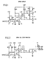
- Figure 1 illustrates a push-pull off-chip driver circuit according to the present invention.
- a low level output from the driver circuit is achieved by turning on the pull-down transistor T10, and a high level driver output is achieved by turning on the pull-up Darlington transistor pair T7, T8.
- a phase splitter is used to provide 180° out-of-phase control signals to the pull-up and pull-down transistors, and this phase splitter includes the transistor T6.
- the transistor T6 When the transistor T6 is conductive, the base potentials of the transistors T7 and T8 will be pulled down to thereby render these pull-up transistors non-conductive, while at the same time providing a base current to the transistor T10 to render that transistor conductive.
- the base potentials of the transistors T 7 , T 8 will be permitted to rise to a high level to render those transistors conductive and pull up the output of the driver circuit, and the supply of base current to the transistor T IO will be cut off.
- driver circuit of Figure 1 The distinctive features of the driver circuit of Figure 1 will now be described.
- most conventional driver circuits employ a resistor coupled between ground and the base of transistor T,o in order to discharge the base of that transistor when the driving current through transistor T 6 is cut-off.
- Such a discharge resistor will also carry current during the time that the transistor T io is being driven into conduction, thus resulting in unnecessary power dissipation.
- the discharge resistor is replaced by the transistor T 3 , which is driven 180° out-of-phase with respect to the phase-splitting transistor T 6 . Accordingly, when the transistor T 6 is conductive to provide the base driving current to the transistor T,o, the transistor T 3 is non-conductive. All of the current will therefore be provided to the base of transistor T 10 , rather than wasting a portion of that current in a pull-down resistor. When the transistor T 6 becomes non-conductive, transistor T 3 turns on to discharge the base of transistor T 10 . Thus, the base of the output transistor T 10 is itself push-pull driven.
- a second distinctive feature of the invention concerns the source of drive current to the pull-down transistor T 10 .
- transistor T 6 would provide the base drive current to the transistor T 10 .
- the resistor R 4 had to have a small value, since a large-valued resistor would not provide transistor T 10 with sufficient output current sinking capabilitiesty and would also delay the turn-on time of that transistor.
- additional transistors T 4 and T s are available for providing the base drive current to the output pull-down transistor T 10 , so that the transistor T 6 can be used primarily for controlling the on or off state of the Darlington pull-up transistor pair T 7 , T s .
- the transistor T 6 when a transition is to be made from a low level driver output to a high level driver output, the transistor T 6 is rendered non-conductive.
- the high resistance of resistor R 4 will limit the base drive current to the transistor T 7 , thereby limiting the up-going transition in the driver output. It should ulso be pointed out that a large value for the resistor R 4 will decrease the amount of current which must be drawn off by the transistor T 6 in order to turn off the transistors T 7 , T 8 .
- an additional transistor T 5 is provided for supplying base drive current to the transistor T jo .
- the transistor T 5 has no collector resistor and is designed to have a larger emitter area than the transistor T 6 , and therefore exhibits a lower output impedance. In addition, it is coupled to a lower supply voltage, +1.7 V, thus providing additional power savings.
- the purpose of the transistor T 4 is to limit instantaneous current surges through the transistor T s and T 6 .
- the connection point between the resistor R 3 and the transistor T 2 would be connected directly to the base of the transistor T 6 , and the transistors T 4 and T s would not be included.
- any surge in the current through the resistor R 3 would be amplified by the current amplification factor ⁇ of the transistor T s , thus resulting in large surges in the base drive current to the pull-down output transistor T 10 .
- transistor T 4 as a diode in Figure 1
- the current through the resistor R 3 becomes a collector current of the transistor T 4 and will not be multiplied by the ⁇ of transistor T 4 .
- a current mirror is established, and this will limit the current through each of the transistors T 5 and T 6 to a value proportional to the current through the resistor R 3 .
- the turn-on time of the transistor T 10 will be limited, thereby controlling the down-going transition in the driver output.
- transistors T 1 , T 4 , T 5 , T 6 and T 10 are all off, while transistors T 2 , T a , T 7 and T 8 are all on, resulting in a high-level driver output.
- the transistor T 2 turns off and the transistors T 4 ⁇ T 6 begin to conduct. Since the combined current of the transistors T 4 ⁇ T 6 is limited to a low multiple of the current through the resistor R 3 , the turn-on time of the transistor T 10 is limited, thereby controlling the down-going transition in the driver output signal.
- transistors T 1 , T 4 , T s , T 6 and T 10 are all on, while transistors T 2 , T 3 , T 7 and T 8 are off, resulting in a low-level driver output.
- a transistor T 2 turns on to con- se.quently turn off the transistors T 4 ⁇ T 6 , and the transistor T 3 turns on to discharge the base of the transistor T 10 and render that transistor non-conductive.
- the large value of resistance R 4 limits the base current to the transistor T 7 , thereby limiting the turn-on time of the Darlington pair T 7 , T s and controlling the up-going transition in the driver output signal.
- FIG. 2 illustrates an open collector embodiment of the driver circuit according to the present invention, which is substantially the same as the embodiment of Figure 1 after removing the circuit components required for the pull-up Darlington pair, i.e. resistors R4-R7, transistors T 7 , T 8 and diode D 1 .
- resistors R4-R7 resistors required for the pull-up Darlington pair
- transistors T 7 , T 8 and diode D 1 The operation of the circuitry of Figure 2 will be readily apparent, and can be briefly described as follows. For high level inputs, transistor T 2 will be conducting to lower the base potential for transistors T 4 -T s and therefore turn these transistors off. Transistor T 3 will be conducting to discharge the base of the pull-down output transistor T 10 , thereby turning off the transistor T,o. This will allow the output potential of the driver circuit to be raised through the off-chip pull-up resistor RL.
- transistor T 2 will turn off and permit a base current to be provided to the transistors T 4- T s through the resistor R 3 having a relatively high resistance value.
- the Darlington pull-up transistor pair T 7 To is not present in the open collector embodiment, and the transistor T 6 is therefore no longer needed to control the on and off states of the pull-up transistors. Accordingly, both of transistors T 5 and T 6 can be connected to the +1.7 V source to provide the desired base drive current to the transistor T,o with a decreased power dissipation.
- the transistor T 4 performs the same current-limiting function as in the embodiment of Figure 1, thereby controlling the pull-down transition in the drive output. As in the embodiment of Figure 1, the transistor T 3 will turn off for a lower level input, thereby permitting all of the current from the transistors T 4 -T s to be provided as a base drive current to the transistor T 10 .
- the transistors T 2 and T 3 will turn-on, the latter transistor discharging the base of the pull-down output transistor T io and allowing the driver output to be pulled up.
- the turning on of transistor T 2 will discharge the bases of the phase-splitter transistors T 4 ⁇ T 6 , thereby cutting off the base current supply to the transistor T io .
Landscapes
- Physics & Mathematics (AREA)
- Engineering & Computer Science (AREA)
- Nonlinear Science (AREA)
- Power Engineering (AREA)
- Computer Hardware Design (AREA)
- Computing Systems (AREA)
- General Engineering & Computer Science (AREA)
- Mathematical Physics (AREA)
- Electronic Switches (AREA)
- Logic Circuits (AREA)
Description
- This invention relates to a low power off-chip driver circuit having controlled output transition times.
- Push-pull and open collector driver circuits are widely used in data processing systems, examples of push-pull driver circuits being found in U.S.
Patent 4 251 737, U.S.Patent 4 092 551, U.S.Patent 4 071 783 and U.S.Patent 4 016 431. From USPatent 3 824 408 a push-pull driver is known the output transistors of which are controlled by push-pull drive means. Examples of open collector driver circuits can be found, for example, in the above-cited U.S.Patent 4 251 737 and in Mathews et al, "Saturated Off-chip Driver for Low-Power Application", IBM Technical Disclosure Bulletin, Vol. 17, No. 10, March 1975, page 2920. - In past years, emphasis has been placed on improving the operating speeds of driver circuits. However, in very high-density, low-end master slices, low power dissipation is frequently of greater significance than high speed. Indeed, since most or all of the critical logic paths are on a single chip, all-out performance is usually not necessary. Instead, high input/output (I/O) count and heat removal constraints mandate low power dissipation.
- A further troublesome characteristic encountered in many driver circuits is that the output transitions may be too fast, and this creates considerable noise on both off-chip nets and on- chip power distributions. The off-chip noise results in restrictive wiring rules.
- The invention as claimed is intended to remedy these drawbacks. It solves the problem of how to design a low power off-chip driver circuit, in which the speeds of the transition in the driver output are controlled.
- In a preferred embodiment this is achieved by a driver circuit in which the current supply to the pull-down driver output transistor is provided through a first transistor coupled to a relatively low potential source and a second control transistor coupled to a higher potential source through a relatively large resistance. The use of a large value for the resistor will decrease power dissipation, and the first transistor will provide the necessary current sinking capability for the pull-down output transistor while also conserving power due to its lower-valued potential source. Power dissipation is further reduced by using a switched transistor to discharge the base of the pull-down output transistor, rather than the commonly used discharge resistor.
- In both push-pull and open collector embodiments of the present invention, an additional transistor is provided with a relatively large collector resistance and is connected in a current mirror fashion with the first and second control transistors. This limits the current supply to the base of the pull-down transistor output to a relatively low multiple of the current mirror resistance, thereby limiting the turn-on of the output transistor and controlling the down-going transition of the output. In the push-pull embodiment, the pull-up of the output is accomplished by a Darlington transistor pair, and the drive current to the Darlington pair is taken from the junction point between the second control transistor and its collector resistance. The turn-on time of the Darlington pair, and consequently the up-going transistion of the driver output, is thus limited by the high collector resistance of the second control transistor.
- The invention is described in detail below with reference to the drawings, in which
- Figure 1 is a brief schematic diagram of a push-pull driver circuit according to the present invention;
- Figure 2 is a schematic diagram of an open collector driver circuit according to the present invention;
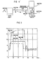
- Figure 3 is a brief diagram of a test configuration for evaluating the driver circuit according to the present invention; and
- Figure 4 is a wave form diagram illustrating measured results from the test configuration of Figure 3.
- The driver circuits according to the present invention are enhanced versions of typical drivers in low-end master slices, and the operation of such circuits is well known. The following description will therefore emphasize the novel features of the invention and will in some areas cover only as much of the conventional driver circuit operation as is necessary for a complete understanding of the invention.
- Figure 1 illustrates a push-pull off-chip driver circuit according to the present invention. As is well known, a low level output from the driver circuit is achieved by turning on the pull-down transistor T10, and a high level driver output is achieved by turning on the pull-up Darlington transistor pair T7, T8. A phase splitter is used to provide 180° out-of-phase control signals to the pull-up and pull-down transistors, and this phase splitter includes the transistor T6. When the transistor T6 is conductive, the base potentials of the transistors T7 and T8 will be pulled down to thereby render these pull-up transistors non-conductive, while at the same time providing a base current to the transistor T10 to render that transistor conductive. On the other hand, when the transistor T6 is non-conductive, the base potentials of the transistors T7, T8 will be permitted to rise to a high level to render those transistors conductive and pull up the output of the driver circuit, and the supply of base current to the transistor TIO will be cut off.
- The distinctive features of the driver circuit of Figure 1 will now be described. First of all, most conventional driver circuits employ a resistor coupled between ground and the base of transistor T,o in order to discharge the base of that transistor when the driving current through transistor T6 is cut-off. Such a discharge resistor, however, will also carry current during the time that the transistor Tio is being driven into conduction, thus resulting in unnecessary power dissipation. Further, it is difficult to discharge the base of transistor T10 quickly enough using a resistor, and any attempt to do so by lowering the value of the discharge resistor will increase the power dissipated by that resistor during the on state of the transistor T10. In the driver circuit according to the present invention, the discharge resistor is replaced by the transistor T3, which is driven 180° out-of-phase with respect to the phase-splitting transistor T6. Accordingly, when the transistor T6 is conductive to provide the base driving current to the transistor T,o, the transistor T3 is non-conductive. All of the current will therefore be provided to the base of transistor T10, rather than wasting a portion of that current in a pull-down resistor. When the transistor T6 becomes non-conductive, transistor T3 turns on to discharge the base of transistor T10. Thus, the base of the output transistor T10 is itself push-pull driven.
- A second distinctive feature of the invention concerns the source of drive current to the pull-down transistor T10. In a conventional driver, transistor T6 would provide the base drive current to the transistor T10. The resistor R4 had to have a small value, since a large-valued resistor would not provide transistor T10 with sufficient output current sinking capabilty and would also delay the turn-on time of that transistor. In the circuit of Figure 1, however, additional transistors T4 and Ts are available for providing the base drive current to the output pull-down transistor T10, so that the transistor T6 can be used primarily for controlling the on or off state of the Darlington pull-up transistor pair T7, Ts. More particularly, when a transition is to be made from a low level driver output to a high level driver output, the transistor T6 is rendered non-conductive. The high resistance of resistor R4 will limit the base drive current to the transistor T7, thereby limiting the up-going transition in the driver output. It should ulso be pointed out that a large value for the resistor R4 will decrease the amount of current which must be drawn off by the transistor T6 in order to turn off the transistors T7, T8.
- Since a large resistance value is used for the resistor R4, the base current to the transistor T10 would ordinarily be inadequate for sufficient output current sinking capability. To compensate for this problem, an additional transistor T5 is provided for supplying base drive current to the transistor Tjo. The transistor T5 has no collector resistor and is designed to have a larger emitter area than the transistor T6, and therefore exhibits a lower output impedance. In addition, it is coupled to a lower supply voltage, +1.7 V, thus providing additional power savings.
- The purpose of the transistor T4 is to limit instantaneous current surges through the transistor Ts and T6. In a conventional driver circuit arrangement, the connection point between the resistor R3 and the transistor T2 would be connected directly to the base of the transistor T6, and the transistors T4 and Ts would not be included. With such an arrangement, any surge in the current through the resistor R3 would be amplified by the current amplification factor β of the transistor Ts, thus resulting in large surges in the base drive current to the pull-down output transistor T10. By connecting transistor T4 as a diode in Figure 1, the current through the resistor R3 becomes a collector current of the transistor T4 and will not be multiplied by the β of transistor T4. Further, with the bases of the transistors T4―T6 connected in common and with their emitters also connected in common, a current mirror is established, and this will limit the current through each of the transistors T5 and T6 to a value proportional to the current through the resistor R3. By limiting the total base drive current to the transistor T10 to a low multiple of the current through the resistor R3, the turn-on time of the transistor T10 will be limited, thereby controlling the down-going transition in the driver output.
- The overall operation of the driver circuit of Figure 1 will be easily understood from the above description. For high-level input signals, transistors T1, T4, T5, T6 and T10 are all off, while transistors T2, Ta, T7 and T8 are all on, resulting in a high-level driver output. When the input changes from a high to a low level, the transistor T2 turns off and the transistors T4―T6 begin to conduct. Since the combined current of the transistors T4―T6 is limited to a low multiple of the current through the resistor R3, the turn-on time of the transistor T10 is limited, thereby controlling the down-going transition in the driver output signal.
- For a low-level input signal, transistors T1, T4, Ts, T6 and T10 are all on, while transistors T2, T3, T7 and T8 are off, resulting in a low-level driver output. When the input changes from a low to a high level, a transistor T2 turns on to con- se.quently turn off the transistors T4―T6, and the transistor T3 turns on to discharge the base of the transistor T10 and render that transistor non-conductive. The large value of resistance R4 limits the base current to the transistor T7, thereby limiting the turn-on time of the Darlington pair T7, Ts and controlling the up-going transition in the driver output signal.
- The driver circuit illustrated in Figure 1 dissipates 3.8 mW nominally, when the following resistor values are employed: R1=10 K, R2=2 K, R3=13.6 K, R4=16.7 K, R5=0.6 K, R6=5 K, and R7=.03 K.
- Figure 2 illustrates an open collector embodiment of the driver circuit according to the present invention, which is substantially the same as the embodiment of Figure 1 after removing the circuit components required for the pull-up Darlington pair, i.e. resistors R4-R7, transistors T7, T8 and diode D1. The operation of the circuitry of Figure 2 will be readily apparent, and can be briefly described as follows. For high level inputs, transistor T2 will be conducting to lower the base potential for transistors T4-Ts and therefore turn these transistors off. Transistor T3 will be conducting to discharge the base of the pull-down output transistor T10, thereby turning off the transistor T,o. This will allow the output potential of the driver circuit to be raised through the off-chip pull-up resistor RL. (This is typically slow enough so that there is no need to provide additional control over the up-going transition). During transition from a a high to a low level input, the transistor T2 will turn off and permit a base current to be provided to the transistors T4-Ts through the resistor R3 having a relatively high resistance value. The Darlington pull-up transistor pair T7, To is not present in the open collector embodiment, and the transistor T6 is therefore no longer needed to control the on and off states of the pull-up transistors. Accordingly, both of transistors T5 and T6 can be connected to the +1.7 V source to provide the desired base drive current to the transistor T,o with a decreased power dissipation. The transistor T4 performs the same current-limiting function as in the embodiment of Figure 1, thereby controlling the pull-down transition in the drive output. As in the embodiment of Figure 1, the transistor T3 will turn off for a lower level input, thereby permitting all of the current from the transistors T4-Ts to be provided as a base drive current to the transistor T10.
- During the transition from low level to high level inputs, the transistors T2 and T3 will turn-on, the latter transistor discharging the base of the pull-down output transistor Tio and allowing the driver output to be pulled up. The turning on of transistor T2 will discharge the bases of the phase-splitter transistors T4―T6, thereby cutting off the base current supply to the transistor Tio.
- Testing of the embodiment of Figure 1 was computer simulated for a configuration as illustrated in Figure 4, and the results were as illustrated in Figure 3. As can be seen from Figure 3, the driver circuit according to the present invention exhibits an average delay of approximately 12 ns. Further, it does so with relatively little off-chip noise and reduced power dissipation.
Claims (4)
Applications Claiming Priority (2)
| Application Number | Priority Date | Filing Date | Title |
|---|---|---|---|
| US06/515,419 US4585953A (en) | 1983-07-20 | 1983-07-20 | Low power off-chip driver circuit |
| US515419 | 1983-07-20 |
Publications (2)
| Publication Number | Publication Date |
|---|---|
| EP0137137A1 EP0137137A1 (en) | 1985-04-17 |
| EP0137137B1 true EP0137137B1 (en) | 1989-06-14 |
Family
ID=24051285
Family Applications (1)
| Application Number | Title | Priority Date | Filing Date |
|---|---|---|---|
| EP84108099A Expired EP0137137B1 (en) | 1983-07-20 | 1984-07-11 | Low power off-chip driver circuit |
Country Status (5)
| Country | Link |
|---|---|
| US (1) | US4585953A (en) |
| EP (1) | EP0137137B1 (en) |
| JP (1) | JPS6027223A (en) |
| CA (1) | CA1250351A (en) |
| DE (1) | DE3478731D1 (en) |
Families Citing this family (3)
| Publication number | Priority date | Publication date | Assignee | Title |
|---|---|---|---|---|
| US4737665A (en) * | 1985-01-15 | 1988-04-12 | Texas Instruments Incorporated | Adjustable speed up circuit for TTL-type gates |
| US4677312A (en) * | 1986-04-25 | 1987-06-30 | International Business Machines Corporation | High voltage swing open collector driver |
| EP0472318A3 (en) * | 1990-08-06 | 1994-08-10 | At & T Corp | Led pulse shaping circuit |
Family Cites Families (29)
| Publication number | Priority date | Publication date | Assignee | Title |
|---|---|---|---|---|
| US3491251A (en) * | 1965-12-20 | 1970-01-20 | Motorola Inc | Logic circuit having noise immunity capability which exceeds one-half the logic swing in both directions |
| US3553486A (en) * | 1968-03-06 | 1971-01-05 | Westinghouse Electric Corp | High noise immunity system for integrated circuits |
| US3609405A (en) * | 1969-02-03 | 1971-09-28 | Goodyear Aerospace Corp | Sharp rise-and-fall time,high-amplitude pulse generator |
| US3602735A (en) * | 1969-10-01 | 1971-08-31 | Sylvania Electric Prod | Pulse shaping circuit for use in integrated circuit networks |
| US3619659A (en) * | 1969-12-02 | 1971-11-09 | Honeywell Inf Systems | Integrator amplifier circuit with voltage regulation and temperature compensation |
| DE2029901A1 (en) * | 1970-06-18 | 1971-12-23 | Siemens Ag | Circuit arrangement for interference signal suppression or attenuation |
| US3656004A (en) * | 1970-09-28 | 1972-04-11 | Ibm | Bipolar capacitor driver |
| DE2102911C3 (en) * | 1971-01-22 | 1982-12-23 | Maschinenfabrik Fahr Ag Gottmadingen, 7702 Gottmadingen | Rotary mower |
| US3710145A (en) * | 1971-02-01 | 1973-01-09 | Raytheon Co | Improved switching circuitry for semiconductor diodes |
| US3824408A (en) * | 1973-07-20 | 1974-07-16 | Microsystems Int Ltd | Driver circuit |
| US3858059A (en) * | 1973-08-01 | 1974-12-31 | Litton Business Systems Inc | High speed driver circuit |
| US3959665A (en) * | 1974-05-29 | 1976-05-25 | The United States Of America As Represented By The Secretary Of The Navy | Logic circuits with interfacing system |
| US3996482A (en) * | 1975-05-09 | 1976-12-07 | Ncr Corporation | One shot multivibrator circuit |
| US4016431A (en) * | 1975-12-31 | 1977-04-05 | International Business Machines Corporation | Optimal driver for LSI |
| US4092551A (en) * | 1976-05-20 | 1978-05-30 | International Business Machines Corporation | A.C. powered speed up circuit |
| JPS5326554A (en) * | 1976-08-24 | 1978-03-11 | Sony Corp | Tr ansistor circuit |
| US4063116A (en) * | 1976-08-26 | 1977-12-13 | Raytheon Company | Temperature compensated current source |
| JPS5368064A (en) * | 1976-11-29 | 1978-06-17 | Fujitsu Ltd | Non-saturation high-speed logical circuit |
| US4071783A (en) * | 1976-11-29 | 1978-01-31 | International Business Machines Corporation | Enhancement/depletion mode field effect transistor driver |
| SE423168B (en) * | 1977-03-07 | 1982-04-13 | Philippe Lataire | DEVICE FOR CONTROL OF THE BASE CURRENT TO POWER TRANSISTORS |
| JPS54156463A (en) * | 1978-05-30 | 1979-12-10 | Nec Corp | Logic circuit |
| JPS556992A (en) * | 1978-06-30 | 1980-01-18 | Ibm | Current drive circuit |
| US4251737A (en) * | 1978-12-29 | 1981-02-17 | International Business Machines Corporation | Dottable active collector driver circuit |
| US4251742A (en) * | 1979-04-09 | 1981-02-17 | Rca Corporation | Current source, as for switching PIN diodes |
| US4321490A (en) * | 1979-04-30 | 1982-03-23 | Fairchild Camera And Instrument Corporation | Transistor logic output for reduced power consumption and increased speed during low to high transition |
| US4330723A (en) * | 1979-08-13 | 1982-05-18 | Fairchild Camera And Instrument Corporation | Transistor logic output device for diversion of Miller current |
| US4301383A (en) * | 1979-10-05 | 1981-11-17 | Harris Corporation | Complementary IGFET buffer with improved bipolar output |
| JPS5819032A (en) * | 1981-07-24 | 1983-02-03 | Nec Corp | Logical gate circuit |
| JPS5844821A (en) * | 1981-09-11 | 1983-03-15 | Nec Corp | Logical gate circuit |
-
1983
- 1983-07-20 US US06/515,419 patent/US4585953A/en not_active Expired - Lifetime
-
1984
- 1984-04-20 JP JP59078831A patent/JPS6027223A/en active Granted
- 1984-06-20 CA CA000457030A patent/CA1250351A/en not_active Expired
- 1984-07-11 EP EP84108099A patent/EP0137137B1/en not_active Expired
- 1984-07-11 DE DE8484108099T patent/DE3478731D1/en not_active Expired
Also Published As
| Publication number | Publication date |
|---|---|
| DE3478731D1 (en) | 1989-07-20 |
| CA1250351A (en) | 1989-02-21 |
| JPS6027223A (en) | 1985-02-12 |
| JPH0336448B2 (en) | 1991-05-31 |
| EP0137137A1 (en) | 1985-04-17 |
| US4585953A (en) | 1986-04-29 |
Similar Documents
| Publication | Publication Date | Title |
|---|---|---|
| JPH02179120A (en) | Load control emitter coupling logic transient driver | |
| US5089724A (en) | High-speed low-power ECL/NTL circuits with AC-coupled complementary push-pull output stage | |
| US4804868A (en) | BiMOS logical circuit | |
| US5247207A (en) | Signal bus line driver circuit | |
| US5550501A (en) | Current buffer circuit with enhanced response speed to input signal | |
| US4430585A (en) | Tristate transistor logic circuit with reduced power dissipation | |
| US4585953A (en) | Low power off-chip driver circuit | |
| EP0316884B1 (en) | Schmitt trigger circuit | |
| US4458162A (en) | TTL Logic gate | |
| US4585959A (en) | Tri-state logic gate having reduced Miller capacitance | |
| EP0224216B1 (en) | An emitter coupled logic circuit | |
| WO1986004197A1 (en) | Tri-state driver circuit | |
| JPH0652496B2 (en) | Low noise transmission line termination circuit | |
| JP2699823B2 (en) | Semiconductor integrated circuit | |
| JP2727649B2 (en) | Logic circuit | |
| KR940005975B1 (en) | Output circuit | |
| US4242605A (en) | Transient array drive for bipolar ROM/PROM | |
| US5408136A (en) | Circuit for providing fast logic transitions | |
| US5278464A (en) | Using delay to obtain high speed current driver circuit | |
| JPH0783253B2 (en) | Low power push-pull driver circuit | |
| JP2775787B2 (en) | Integrated circuit | |
| JPH04346515A (en) | Low threshold bicmos logic circuit | |
| JPH04227326A (en) | Hysteresis ttl buffer circuit for high-speed inversion | |
| JP2551609B2 (en) | Circuit | |
| JP2794024B2 (en) | High speed sense amplifier |
Legal Events
| Date | Code | Title | Description |
|---|---|---|---|
| PUAI | Public reference made under article 153(3) epc to a published international application that has entered the european phase |
Free format text: ORIGINAL CODE: 0009012 |
|
| 17P | Request for examination filed |
Effective date: 19841123 |
|
| AK | Designated contracting states |
Designated state(s): DE FR GB IT |
|
| 17Q | First examination report despatched |
Effective date: 19870525 |
|
| GRAA | (expected) grant |
Free format text: ORIGINAL CODE: 0009210 |
|
| AK | Designated contracting states |
Kind code of ref document: B1 Designated state(s): DE FR GB IT |
|
| REF | Corresponds to: |
Ref document number: 3478731 Country of ref document: DE Date of ref document: 19890720 |
|
| ET | Fr: translation filed | ||
| ITF | It: translation for a ep patent filed | ||
| PLBE | No opposition filed within time limit |
Free format text: ORIGINAL CODE: 0009261 |
|
| STAA | Information on the status of an ep patent application or granted ep patent |
Free format text: STATUS: NO OPPOSITION FILED WITHIN TIME LIMIT |
|
| 26N | No opposition filed | ||
| ITTA | It: last paid annual fee | ||
| PGFP | Annual fee paid to national office [announced via postgrant information from national office to epo] |
Ref country code: GB Payment date: 19940613 Year of fee payment: 11 |
|
| PGFP | Annual fee paid to national office [announced via postgrant information from national office to epo] |
Ref country code: FR Payment date: 19940627 Year of fee payment: 11 |
|
| PGFP | Annual fee paid to national office [announced via postgrant information from national office to epo] |
Ref country code: DE Payment date: 19940716 Year of fee payment: 11 |
|
| PG25 | Lapsed in a contracting state [announced via postgrant information from national office to epo] |
Ref country code: GB Effective date: 19950711 |
|
| GBPC | Gb: european patent ceased through non-payment of renewal fee |
Effective date: 19950711 |
|
| PG25 | Lapsed in a contracting state [announced via postgrant information from national office to epo] |
Ref country code: DE Effective date: 19960402 |
|
| PG25 | Lapsed in a contracting state [announced via postgrant information from national office to epo] |
Ref country code: FR Effective date: 19960430 |
|
| REG | Reference to a national code |
Ref country code: FR Ref legal event code: ST |
|
| REG | Reference to a national code |
Ref country code: FR Ref legal event code: ST |
|
| REG | Reference to a national code |
Ref country code: FR Ref legal event code: ST |