EP0135957B1 - Acoustic surface wave device - Google Patents
Acoustic surface wave device Download PDFInfo
- Publication number
- EP0135957B1 EP0135957B1 EP19840201202 EP84201202A EP0135957B1 EP 0135957 B1 EP0135957 B1 EP 0135957B1 EP 19840201202 EP19840201202 EP 19840201202 EP 84201202 A EP84201202 A EP 84201202A EP 0135957 B1 EP0135957 B1 EP 0135957B1
- Authority
- EP
- European Patent Office
- Prior art keywords
- centre
- frequency
- transducer
- electrodes
- acoustic
- Prior art date
- Legal status (The legal status is an assumption and is not a legal conclusion. Google has not performed a legal analysis and makes no representation as to the accuracy of the status listed.)
- Expired
Links
Images

Classifications
-
- H—ELECTRICITY
- H03—ELECTRONIC CIRCUITRY
- H03H—IMPEDANCE NETWORKS, e.g. RESONANT CIRCUITS; RESONATORS
- H03H9/00—Networks comprising electromechanical or electro-acoustic elements; Electromechanical resonators
- H03H9/46—Filters
- H03H9/64—Filters using surface acoustic waves
- H03H9/6423—Means for obtaining a particular transfer characteristic
- H03H9/643—Means for obtaining a particular transfer characteristic the transfer characteristic being determined by reflective or coupling array characteristics
-
- H—ELECTRICITY
- H03—ELECTRONIC CIRCUITRY
- H03H—IMPEDANCE NETWORKS, e.g. RESONANT CIRCUITS; RESONATORS
- H03H9/00—Networks comprising electromechanical or electro-acoustic elements; Electromechanical resonators
- H03H9/02—Details
- H03H9/125—Driving means, e.g. electrodes, coils
- H03H9/145—Driving means, e.g. electrodes, coils for networks using surface acoustic waves
-
- H—ELECTRICITY
- H03—ELECTRONIC CIRCUITRY
- H03H—IMPEDANCE NETWORKS, e.g. RESONANT CIRCUITS; RESONATORS
- H03H9/00—Networks comprising electromechanical or electro-acoustic elements; Electromechanical resonators
- H03H9/02—Details
- H03H9/02535—Details of surface acoustic wave devices
- H03H9/02637—Details concerning reflective or coupling arrays
- H03H9/02685—Grating lines having particular arrangements
- H03H9/02708—Shifted grating lines
-
- H—ELECTRICITY
- H03—ELECTRONIC CIRCUITRY
- H03H—IMPEDANCE NETWORKS, e.g. RESONANT CIRCUITS; RESONATORS
- H03H9/00—Networks comprising electromechanical or electro-acoustic elements; Electromechanical resonators
- H03H9/02—Details
- H03H9/02535—Details of surface acoustic wave devices
- H03H9/02637—Details concerning reflective or coupling arrays
- H03H9/02685—Grating lines having particular arrangements
- H03H9/0274—Intra-transducers grating lines
Definitions
- This invention relates to an acoustic surface wave filter device comprising a piezo-electric substrate for propagating acoustic surface waves, including waves having the centre-frequency of the frequency response characteristic of the device, at a surface thereof, a first bi-directional electro-acoustic transducer formed on said surface for launching acoustic surface waves, including waves having said centre-frequency, along first and second propagation paths at said surface, a second bidirectional electro-acoustic transducer formed on said surface for receiving acoustic surface waves, including waves having said centre-frequency, propagating along said first and second paths at respective input ports thereof, and at least one pair of reflective multi-strip couplers formed on said surface, the two couplers of the or each pair being associated with said first and second paths respectively for receiving acoustic surface wave energy having said centre-frequency propagating along a portion of the associated path and relaunching at least part of that energy as acoustic surface waves along another portion of the associated path, each transducer comprising an inter
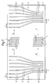
- a device of this kind which will be referred to as a device of the kind set forth, is known from, for example, Fig. 5 of published French patent application serial number 2290785 and is shown in Fig. 1 of the accompanying diagrammatic drawings.
- an acoustic surface wave device comprises a piezo-electric substrate 1 on the top surface of which are formed first and second transducers 2 and 3 respectively for launching and receiving, respectively, surface acoustic waves at said top surface.
- Each transducer comprises an interdigital array of electrodes 4, 5 and 6, 7 respectively as shown, an input signal being applied between the two combs which make up the transducer 2 and an output signal being generated between the two combs which make up the transducer 3.
- Each transducer is bidirectional, i.e. acoustic surface waves are propagated by transducer 2 simultaneously in two oppositely-directed tracks the length directions of which extend at right angles to the electrodes 4 and 5.
- tracks 8 and 9 are indicated by arrows 8 and 9 respectively.
- transducer 3 receives and transduces simultaneously acoustic surface waves incident thereon from two oppositely directed tracks the length directions of which extend at right angles to the electrodes 6 and 7.
- tracks 10 and 11 are indicated by arrows 10 and 11 respectively.
- Tracks 8 and 10 constitute first and second portions respectively of a first surface acoustic wave propagation path from transducer 2 to transducer 3
- tracks 9 and 11 constitute first and second portions respectively of a second surface acoustic wave propagation path from transducer 2 to transducer 3.
- a pair of reflective multistrip couplers 12 and 13 are also formed on the top surface of substrate 1.
- Coupler 12 receives surface acoustic wave energy propagating along track 8 and relaunches at least part of that energy along track 10.
- coupler 13 receives surface acoustic wave energy of a given frequency propagating along track 9 and relaunches at least part of that energy along track 11.
- ⁇ o is the length of acoustic surface waves which are launched by transducer 2 along tracks 8 and 9 when an electric input signal having a frequency (the "given frequency") equal to the centre-frequency of the desired frequency response characteristic of the device (which operates as a filter) is applied to transducer 2.
- a and c may, for example, equal 2/3 ⁇ o , in which case b and d will equal 1/3 ⁇ o .
- couplers 12 and 13 contain a sufficient number of strips 14 and 15 respectively substantially all of the energy launched in both tracks 8 and 9 by transducer 2 will be transferred to tracks 10 and 11 respectively, and hence to transducer 3, enabling the device of Fig. 1 to have a lower insertion loss at the centre frequency than would be the case if the energy launched in one direction by transducer 2 were simply dissipated, for example by means of absorbent material.
- This potentially low insertion loss is very useful, for example, when the device is used to provide front-end selectivity in radio or other receivers, but can be achieved only if the transducers are correctly matched to the external circuits to which they are connected in operation.
- this entails the provision of matching networks as external components, which networks may have to be individually tuned, thus adding to the cost of providing the filter. It is an object of the invention to mitigate this disadvantage.
- the invention provides an acoustic surface wave filter device comprising a piezo-electric substrate for propagating acoustic surface waves, including waves having the centre-frequency of the frequency response characteristic of the device, at a surface thereof, a first bi-directional electro-acoustic transducer formed on said surface for launching acoustic surface waves, including waves having said centre-frequency, along first and second propagation paths at said surface, a second bidirectionalelectro-acoustic transducer formed on said surface for receiving acoustic surface waves, including waves having said centre-frequency, propagating along said first and second paths at respective input ports thereof, and at least one pair of reflective multi-strip couplers formed on said surface, the two couplers of the or each pair being associated with said first and second paths respectively for receiving acoustic surface wave energy having said centre-frequency propagating along a portion of the associated path and relaunching at least part of that energy as acoustic surface waves along another portion of the associated path, each transducer comprising an
- the impedance of the said corresponding transducer at the centre-frequency be equal to that of free space, i.e. in addition to being real, be substantially equal to 50 ohms.
- the conductance versus frequency characteristic of each transducer depends on the size of the aperture thereof so, accordingly, the size of the aperture of said corresponding transducer may be such that the impedance of corresponding first transducer is substantially equal to 50 ohms at said centre-frequency.
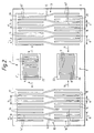
- Fig. 2 The configuration shown in Fig. 2, in which corresponding components have been given the same references as their counterparts in Fig. 1, is very similar to that shown in Fig. 1, the main difference being that the reflective multistrip couplers are of the kind disclosed in coopending British patent applications 8219372 and 8219373 (PHB 32892 and PHB 32893; European patent application 83200986.4), i.e. of the kind in which the centre-to-centre distances of the strips 14 and 15 where they overlay the tracks 8-11 are alternately large ( b or d ) and small ( a or c ), each pair of strips which have a large centre-to-centre distance in one track having a small centre-to-centre distance in the other track.
- the reflective multistrip couplers are of the kind disclosed in coopending British patent applications 8219372 and 8219373 (PHB 32892 and PHB 32893; European patent application 83200986.4), i.e. of the kind in which the
- each pair of relatively widely spaced strip portions 14', 14'', 15' and 15'' has, situated therebetween, a further pair of strips 16 which are connected to a bus-bar 17, 18, 19 or 20, these bus-bars being grounded in operation.
- a regular succession of parallel strips extending along each path 8, 9, 10 and 11, the centre-to-centre distances between adjacent strips in each succession being ⁇ o /4 and the strip widths being ⁇ o /8.
- the transducers 2 and 3 are of the double-finger type, pairs of successive electrodes 4, 5, 6 and 7 being connected to the same bus-bar 21, 22, 23 or 24, this bus-bar being different from that to which the adjacent pair is connected.
- This structure is known from, for example, the paper entitled “Applications of double electrodes in acoustic surface wave device design” by T. W. Bristol et. al. presented to the IEEE Ultrasonics Symposium, October 1972.
- the centre-to-centre distances of the electrodes 4, 5, 6 and 7 are in this case a few percent greater than ⁇ o /4 (in Fig. 1 they are ⁇ o /2).
- Fig. 2 shows, for clarity, only the general configuration of an embodiment of the invention.
- the substrate was 128 o Y-rotated X-propagating lithium niobate
- the various electrodes and bus bars being formed thereon in known manner by a process of photolithography
- transducer 2 included twenty pairs 4,4,5,5 of double fingers (eighty electrodes in all) and transducer 3 similarly included twenty pairs 6,6,7,7 of double fingers.
- Coupler 12 included 150 electrodes 14 and, similarly, coupler 13 included 150 electrodes 15, this number of electrodes being sufficient to ensure that the reflection coefficient of each coupler is substantially 100% at a frequency corresponding to ⁇ o ; if a reflection coefficient of 90% is satisfactory in a particular case the number could be reduced to approximately 100. (Less electrodes would be required with a different lithium niobate cut which is such as to give higher coupling).
- ⁇ o corresponded to approximately 164 MHz.
- the sizes of the apertures of transducers 2 and 3 (corresponding to the lengths of the electrodes 4, 5, 6 and 7) were 73 ⁇ o .
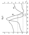
- the susceptance B (normalised to 1/50 ohms) versus frequency f characteristic of each of the transducers 2 and 3 was as shown by curve 25 of Fig. 3, and the conductance G (normalised to 1/50 ohms) of each was as shown by curve 26 of Fig. 3.
- the impedance of each transducer was substantially real within the range R between approximately 162.5 MHz and 165.5 MHz, i.e.
- the size of which band is approximately 1% of the frequency corresponding to ⁇ o for the coupler configuration and substrate material and cut quoted, and was equal to 50 ohms at approximately 164 MHz.
- the position along the frequency axis of the minimum in the susceptance curve depends on the centre-to-centre spacing and number of the electrodes of the transducers. For transducers with uniform centre-to-centre spacings of their electrodes this position in general lies some way above their synchronous frequency, moving closer to the synchronous frequency as the number of electrodes is increased.
- the position of the minimum in the susceptance curve along the susceptance axis depends on several factors.
- the relevant transducer is apodized; if it is, the number of transducer electrodes required to produce a given value of susceptance at the minimum will in general be larger. As another example it depends on the particular substrate material and particular cut employed.
- the number of transducer electrodes required to produce a given value of susceptance at the minimum will in general be increased. As yet another example it depends on the mark-to-space ratio of the succession of transducer electrodes. For this reason the actual transducer configuration required to give the desired result in a particular situation will have to be individually calculated.
- Fig. 4 in which similar components are denoted by the same reference numerals as their counterparts in Fig. 2, shows the general configuration of another embodiment of the invention. Instead of including just one pair of reflective multistrip couplers 12 and 13, this configuration includes three such pairs, and 29, 30 respectively. These couplers are all identical, and identical to the couplers 12 and 13 described with reference to Fig. 2. Moreover the substrate 1 and transducers 2 and 3 are identical to the substrate 1 and transducers 2 and 3 described with reference to Fig. 2. A rectangular layer 31 of acoustic surface wave absorbent material, for example silicone rubber, is provided between the couplers 27 and 28 to prevent cross-talk from occuring at frequencies different from the centre-frequency of the device response.
- acoustic surface wave absorbent material for example silicone rubber
- the reflective multistrip couplers may, as an alternative, have one of the other configurations disclosed in the aforementioned patent applications 8219372 and 8219373 or as shown in Fig. 1 of the accompanying drawings.
- each pair of mutually adjacent strips 16 is replaced by a single strip the centre-line of which is situated midway between the two strips which it replaces, and the width of each strip is increased to ⁇ o /6, so that there is now a regular succession of parallel strips extending along each path 8, 9, 10 and 11, the centre-to-centre distances of adjacent strips in each succession being ⁇ o /3.
Landscapes
- Physics & Mathematics (AREA)
- Acoustics & Sound (AREA)
- Surface Acoustic Wave Elements And Circuit Networks Thereof (AREA)
Description
- This invention relates to an acoustic surface wave filter device comprising a piezo-electric substrate for propagating acoustic surface waves, including waves having the centre-frequency of the frequency response characteristic of the device, at a surface thereof, a first bi-directional electro-acoustic transducer formed on said surface for launching acoustic surface waves, including waves having said centre-frequency, along first and second propagation paths at said surface, a second bidirectional electro-acoustic transducer formed on said surface for receiving acoustic surface waves, including waves having said centre-frequency, propagating along said first and second paths at respective input ports thereof, and at least one pair of reflective multi-strip couplers formed on said surface, the two couplers of the or each pair being associated with said first and second paths respectively for receiving acoustic surface wave energy having said centre-frequency propagating along a portion of the associated path and relaunching at least part of that energy as acoustic surface waves along another portion of the associated path, each transducer comprising an interdigital array of electrodes which extend at right angles to the length directions of the propagation paths where those paths adjoin the relevant transducer, the electrodes in at least one said array having a uniform centre-to-centre distance.
- A device of this kind, which will be referred to as a device of the kind set forth, is known from, for example, Fig. 5 of published French patent application serial number 2290785 and is shown in Fig. 1 of the accompanying diagrammatic drawings.
- In Fig. 1 (which is a diagrammatic plan view) an acoustic surface wave device comprises a piezo-
electric substrate 1 on the top surface of which are formed first andsecond transducers electrodes transducer 2 and an output signal being generated between the two combs which make up thetransducer 3. Each transducer is bidirectional, i.e. acoustic surface waves are propagated bytransducer 2 simultaneously in two oppositely-directed tracks the length directions of which extend at right angles to theelectrodes arrows transducer 3 receives and transduces simultaneously acoustic surface waves incident thereon from two oppositely directed tracks the length directions of which extend at right angles to theelectrodes arrows Tracks transducer 2 to transducer 3, andtracks reflective multistrip couplers substrate 1.Coupler 12 receives surface acoustic wave energy propagating alongtrack 8 and relaunches at least part of that energy alongtrack 10. Similarly,coupler 13 receives surface acoustic wave energy of a given frequency propagating alongtrack 9 and relaunches at least part of that energy alongtrack 11. To this end the portions 14' of theconductive strips 14 of thecoupler 12 which extend over and at right angles to thetrack 8 have a centre-to-centre distance a and the corresponding portions 14'' of thestrips 14 of thecoupler 12 which extend over and at right angles to thetrack 10 have a different centre-to-centre distance b, where
tracks conductive strips 15 of thecoupler 13 which extend over and at right angles to thetrack 9 have a centre-to-centre distance c and the corresponding portions 15'' of thestrips 15 of thecoupler 13 which extend over and at right-angles to thetrack 11 have a different centre-to-centre distance d, where again
couplers strips tracks transducer 2 will be transferred totracks transducer 2 were simply dissipated, for example by means of absorbent material. It can be arranged that, over a limited range of frequencies (approximately 1% if thesubstrate 1 is 128o Y-rotated X-propagating lithium niobate and approximately 2% if thesubstrate 1 is 41o Y-rotated X-propagating lithium niobate) almost 100% of the energy propagating intracks tracks couplers - This potentially low insertion loss is very useful, for example, when the device is used to provide front-end selectivity in radio or other receivers, but can be achieved only if the transducers are correctly matched to the external circuits to which they are connected in operation. With the known devices this entails the provision of matching networks as external components, which networks may have to be individually tuned, thus adding to the cost of providing the filter. It is an object of the invention to mitigate this disadvantage.
- The invention provides an acoustic surface wave filter device comprising a piezo-electric substrate for propagating acoustic surface waves, including waves having the centre-frequency of the frequency response characteristic of the device, at a surface thereof, a first bi-directional electro-acoustic transducer formed on said surface for launching acoustic surface waves, including waves having said centre-frequency, along first and second propagation paths at said surface, a second bidirectionalelectro-acoustic transducer formed on said surface for receiving acoustic surface waves, including waves having said centre-frequency, propagating along said first and second paths at respective input ports thereof, and at least one pair of reflective multi-strip couplers formed on said surface, the two couplers of the or each pair being associated with said first and second paths respectively for receiving acoustic surface wave energy having said centre-frequency propagating along a portion of the associated path and relaunching at least part of that energy as acoustic surface waves along another portion of the associated path, each transducer comprising an interdigital array of electrodes which extend at right angles to the length directions of the propagation paths where those paths adjoin the relevant tranducer, the electrodes in at least one said array having a uniform centre-to-centre distance, characterized in that said centre-to-centre distance of the electrodes in said at least one said array is such that the synchronous frequency of the corresponding transducer lies below said centre-frequency, and said centre-to-centre distance and the number of electrodes in the corresponding array are such that the susceptance versus frequency characteristic of the corresponding transducer exhibits a minimum which substantially coincides with said centre-frequency and the value of the susceptance at this minimum is substantially zero.
- It has now been recognised that, because the frequency response characteristic of a device of the kind set forth is determined mainly by the reflective multi-strip couplers, there is a considerable amount of latitude available in the design of the transducers. Because of this, and because the susceptance versus frequency characteristic of each transducer exhibits a minimum at a frequency which depends on the centre-to-centre distances and number of the electrodes in the corresponding array, the value of the susceptance depending on the number of electrodes in the corresponding array, it is possible to construct one or both transducers in such a way that its impedance is substantially real within a range of frequencies which contains the centre-frequency of the frequency response characteristic of the device, thereby eliminating the need for external tuned matching networks. In other words it can be arranged that the motional inductance of one or both transducers substantially exactly tunes out the static capacitance thereof at said centre-frequency.
- When the device is to be used to provide front-end selectivity in a radio or other receiver it will often be required that the impedance of the said corresponding transducer at the centre-frequency be equal to that of free space, i.e. in addition to being real, be substantially equal to 50 ohms. The conductance versus frequency characteristic of each transducer depends on the size of the aperture thereof so, accordingly, the size of the aperture of said corresponding transducer may be such that the impedance of corresponding first transducer is substantially equal to 50 ohms at said centre-frequency.
- Embodiments of the invention will now be described, by way of example, with reference to the accompanying diagrammatic drawings, in which
- Fig. 1 shows the known device previously referred to ,
- Fig. 2 shows the configuration of a first embodiment of the invention,
- Fig. 3 shows conductance and susceptance versus frequency characteristics for transducers in the embodiment to be described with reference to Fig. 2, and
- Fig. 4 shows the configuration of a second embodiment of the invention.
- The configuration shown in Fig. 2, in which corresponding components have been given the same references as their counterparts in Fig. 1, is very similar to that shown in Fig. 1, the main difference being that the reflective multistrip couplers are of the kind disclosed in coopending British patent applications 8219372 and 8219373 (PHB 32892 and PHB 32893; European patent application 83200986.4), i.e. of the kind in which the centre-to-centre distances of the
strips 
 where λo is as defined above. Each pair of relatively widely spaced strip portions 14', 14'', 15' and 15'' has, situated therebetween, a further pair of
strips 16 which are connected to a bus-bar path transducers successive electrodes bar electrodes - Fig. 2 shows, for clarity, only the general configuration of an embodiment of the invention. In the actual embodiment, in which the substrate was 128o Y-rotated X-propagating lithium niobate, the various electrodes and bus bars being formed thereon in known manner by a process of photolithography,
transducer 2 included twentypairs transducer 3 similarly included twentypairs Coupler 12 included 150electrodes 14 and, similarly,coupler 13 included 150electrodes 15, this number of electrodes being sufficient to ensure that the reflection coefficient of each coupler is substantially 100% at a frequency corresponding to λo; if a reflection coefficient of 90% is satisfactory in a particular case the number could be reduced to approximately 100. (Less electrodes would be required with a different lithium niobate cut which is such as to give higher coupling). λo corresponded to approximately 164 MHz. The sizes of the apertures oftransducers 2 and 3 (corresponding to the lengths of theelectrodes - The susceptance B (normalised to 1/50 ohms) versus frequency f characteristic of each of the
transducers curve 25 of Fig. 3, and the conductance G (normalised to 1/50 ohms) of each was as shown bycurve 26 of Fig. 3. Thus the impedance of each transducer was substantially real within the range R between approximately 162.5 MHz and 165.5 MHz, i.e. over the band of frequencies within which thecouplers - The position along the frequency axis of the minimum in the susceptance curve depends on the centre-to-centre spacing and number of the electrodes of the transducers. For transducers with uniform centre-to-centre spacings of their electrodes this position in general lies some way above their synchronous frequency, moving closer to the synchronous frequency as the number of electrodes is increased. The position of the minimum in the susceptance curve along the susceptance axis depends on several factors. For example it will correspond to a higher value of susceptance, resulting in the susceptance versus frequency characteristic not touching or crossing the axis at all, if the number of electrodes included in the corresponding transducer is decreased, and will correspond to a lower value of susceptance, resulting in the susceptance versus frequency characteristic crossing the axis too steeply, if the number of electrodes included in the corresponding transducer is increased. As another example it depends on whether or not the relevant transducer is apodized; if it is, the number of transducer electrodes required to produce a given value of susceptance at the minimum will in general be larger. As another example it depends on the particular substrate material and particular cut employed. If the material and/or cut are such that the coupling between the substrate and the various electrodes is weaker than in the example quoted, the number of transducer electrodes required to produce a given value of susceptance at the minimum will in general be increased. As yet another example it depends on the mark-to-space ratio of the succession of transducer electrodes. For this reason the actual transducer configuration required to give the desired result in a particular situation will have to be individually calculated. For this purpose reference may be made to the general treatment given in the article entitled "Analysis of generation and detection of surface and bulk acoustic waves by interdigital transducers" by Milsom et al contained in IEEE Transactions on Sonics and Ultrasonics, SU 24, May 1977, pages 147-166, particularly equations (1)-(38) therein. The real part of the impedance of each transducer in general scales inversely with the lengths of its electrodes.
- Fig. 4, in which similar components are denoted by the same reference numerals as their counterparts in Fig. 2, shows the general configuration of another embodiment of the invention. Instead of including just one pair of
reflective multistrip couplers couplers substrate 1 andtransducers substrate 1 andtransducers rectangular layer 31 of acoustic surface wave absorbent material, for example silicone rubber, is provided between thecouplers - In all the embodiments described with reference to Figs. 2 and 4 the reflective multistrip couplers may, as an alternative, have one of the other configurations disclosed in the aforementioned patent applications 8219372 and 8219373 or as shown in Fig. 1 of the accompanying drawings. In particular, the
couplers strips adjacent strips 16 is replaced by a single strip the centre-line of which is situated midway between the two strips which it replaces, and the width of each strip is increased to λo/6, so that there is now a regular succession of parallel strips extending along eachpath strips path strips couplers
Claims (2)
- An acoustic surface wave filter device comprising a piezo-electric substrate for propagating acoustic surface waves, including waves having the centre-frequency of the frequency response characteristic of the device, at a surface thereof, a first bi-directional electro-acoustic transducer formed on said surface for launching acoustic surface waves, including waves having said centre-frequency, along first and second propagation paths at said surface, a second bidirectional electro-acoustic transducer formed on said surface for receiving acoustic surface waves, including waves having said centre-frequency, propagating along said first and second paths at respective input ports thereof, and at least one pair of reflective multi-strip couplers formed on said surface, the two couplers of the or each pair being associated with said first and second paths respectively for receiving acoustic surface wave energy having said centre-frequency propagating along a portion of the associated path and relaunching at least part of that energy as acoustic surface waves along another portion of the associated path, each transducer comprising an interdigital array of electrodes which extend at right angles to the length directions of the propagation paths where those paths adjoin the relevant tranducer, the electrodes in at least one said array having a uniform centre-to-centre distance, characterized in that said centre-to-centre distance of the electrodes in said at least one said array is such that the synchronous frequency of the corresponding transducer lies below said centre-frequency, and said centre-to-centre distance and the number of electrodes in the corresponding array are such that the susceptance versus frequency characteristic of the corresponding transducer exhibits a minimum which substantially coincides with said centre-frequency and the value of the susceptance at this minimum is substantially zero.
- A device as claimed in Claim 1, wherein the size of the aperture of said corresponding transducer is such that the impedance of said corresponding transducer is substantially 50 ohms at said centre-frequency.
Applications Claiming Priority (2)
| Application Number | Priority Date | Filing Date | Title |
|---|---|---|---|
| GB8323294 | 1983-08-31 | ||
| GB08323294A GB2145892A (en) | 1983-08-31 | 1983-08-31 | Surface acoustic wave device |
Publications (3)
| Publication Number | Publication Date |
|---|---|
| EP0135957A2 EP0135957A2 (en) | 1985-04-03 |
| EP0135957A3 EP0135957A3 (en) | 1987-01-28 |
| EP0135957B1 true EP0135957B1 (en) | 1991-11-06 |
Family
ID=10548082
Family Applications (1)
| Application Number | Title | Priority Date | Filing Date |
|---|---|---|---|
| EP19840201202 Expired EP0135957B1 (en) | 1983-08-31 | 1984-08-20 | Acoustic surface wave device |
Country Status (5)
| Country | Link |
|---|---|
| US (1) | US4727275A (en) |
| EP (1) | EP0135957B1 (en) |
| JP (1) | JPS6072312A (en) |
| DE (1) | DE3485238D1 (en) |
| GB (1) | GB2145892A (en) |
Families Citing this family (7)
| Publication number | Priority date | Publication date | Assignee | Title |
|---|---|---|---|---|
| JPH01101718A (en) * | 1987-10-14 | 1989-04-19 | Clarion Co Ltd | Surface acoustic wave device |
| US5663695A (en) * | 1994-10-31 | 1997-09-02 | Ngk Insulators, Ltd. | Surface acoustic wave filter device and transducer therefor |
| JP3315646B2 (en) * | 1998-06-19 | 2002-08-19 | 富士通株式会社 | Surface acoustic wave filter |
| JP4718718B2 (en) * | 2001-05-10 | 2011-07-06 | 株式会社ミツバ | Carbon substrate manufacturing method |
| JP3934544B2 (en) * | 2002-04-11 | 2007-06-20 | 富士通株式会社 | Elastic wave observation device |
| KR20040000967A (en) * | 2002-06-26 | 2004-01-07 | 엘지이노텍 주식회사 | Saw filter |
| FR3100999B1 (en) * | 2019-09-25 | 2022-07-15 | Lille Ecole Centrale | Electroacoustic device |
Family Cites Families (13)
| Publication number | Priority date | Publication date | Assignee | Title |
|---|---|---|---|---|
| US3886504A (en) * | 1974-05-20 | 1975-05-27 | Texas Instruments Inc | Acoustic surface wave resonator devices |
| US4126837A (en) * | 1974-07-01 | 1978-11-21 | Nippon Telegraph And Telephone Public Corporation | Impedance element and band-rejection filter using the same |
| US4038614A (en) * | 1975-06-16 | 1977-07-26 | Hughes Aircraft Company | Fractional efficiency coupler |
| US4079342A (en) * | 1976-09-15 | 1978-03-14 | Sperry Rand Corporation | Fanned multistrip coupler filters |
| GB1551530A (en) * | 1977-05-12 | 1979-08-30 | Standard Telephones Cables Ltd | Surface acoustic wave resonamt transducer device |
| US4130813A (en) * | 1977-05-23 | 1978-12-19 | Raytheon Company | Surface wave device having enhanced reflectivity gratings |
| JPS55112023A (en) * | 1980-01-21 | 1980-08-29 | Hitachi Ltd | Elastic surface wave filter |
| GB2070379B (en) * | 1980-02-21 | 1984-05-16 | Philips Electronic Associated | Acoustic wave bandpass electrical filters |
| US4370633A (en) * | 1981-01-19 | 1983-01-25 | U.S. Philips Corporation | Acoustic wave bandpass electrical filters |
| JPS57119509A (en) * | 1981-01-19 | 1982-07-26 | Toshiba Corp | Surface acoustic wave resonator |
| DE3130154A1 (en) * | 1981-07-30 | 1983-02-17 | Siemens Ag | Surface acoustic wave arrangement with integrated matching network |
| GB2123636A (en) * | 1982-07-05 | 1984-02-01 | Philips Electronic Associated | Acoustic surface wave device including a reflective multistrip coupler |
| US4510471A (en) * | 1982-07-05 | 1985-04-09 | U.S. Philips Corporation | Acoustic surface wave device including a reflective multistrip coupler |
-
1983
- 1983-08-31 GB GB08323294A patent/GB2145892A/en not_active Withdrawn
-
1984
- 1984-08-17 US US06/641,644 patent/US4727275A/en not_active Expired - Fee Related
- 1984-08-20 EP EP19840201202 patent/EP0135957B1/en not_active Expired
- 1984-08-20 DE DE8484201202T patent/DE3485238D1/en not_active Expired - Lifetime
- 1984-08-28 JP JP59177616A patent/JPS6072312A/en active Pending
Also Published As
| Publication number | Publication date |
|---|---|
| US4727275A (en) | 1988-02-23 |
| GB2145892A (en) | 1985-04-03 |
| EP0135957A3 (en) | 1987-01-28 |
| GB8323294D0 (en) | 1983-10-05 |
| JPS6072312A (en) | 1985-04-24 |
| DE3485238D1 (en) | 1991-12-12 |
| EP0135957A2 (en) | 1985-04-03 |
Similar Documents
| Publication | Publication Date | Title |
|---|---|---|
| EP0056690B1 (en) | Surface acoustic wave resonator device | |
| EP0184508B1 (en) | Surface acoustic wave transducer | |
| CA1060962A (en) | Surface wave filters with coupled resonators | |
| US4146851A (en) | Acoustic surface wave device | |
| US4340834A (en) | Surface acoustic wave resonator device | |
| US4727275A (en) | Acoustic surface wave device | |
| US4659955A (en) | Surface-propagating acoustic wave device | |
| US4902925A (en) | Reflectionless transducer | |
| EP0044732A2 (en) | Acoustic surface wave transducer with improved inband frequency characteristics | |
| US4511866A (en) | Acoustic surface wave device | |
| EP0063839B1 (en) | Acoustic wave bandpass electrical filters | |
| EP0103932A2 (en) | Acoustic surface wave device | |
| US4357584A (en) | Acoustic wave devices | |
| US4370633A (en) | Acoustic wave bandpass electrical filters | |
| US4185218A (en) | Piezoelectric acoustic surface wave filter coupler | |
| EP0255263B1 (en) | Transducer | |
| US4510471A (en) | Acoustic surface wave device including a reflective multistrip coupler | |
| US3873946A (en) | Acoustic surface wave tapped delay line | |
| Marshall et al. | Observed properties of an acoustic-surface-wave multistrip coupler | |
| US4511867A (en) | Acoustic surface wave device including a reflective multistrip coupler | |
| US5545940A (en) | Multitrack transversely folded surface acoustic wave structure | |
| US4290033A (en) | Shallow bulk acoustic wave devices employing energy trapping | |
| EP0098661B1 (en) | Acoustic surface wave device including a reflective multistrip coupler | |
| US4191934A (en) | High efficiency wide band surface acoustic wave coupler processors | |
| EP0314297A2 (en) | Three-transducer saw device including one or two apodized transducers having minimum-phase and maximum-phase impulse responses |
Legal Events
| Date | Code | Title | Description |
|---|---|---|---|
| PUAI | Public reference made under article 153(3) epc to a published international application that has entered the european phase |
Free format text: ORIGINAL CODE: 0009012 |
|
| AK | Designated contracting states |
Designated state(s): DE FR GB IT SE |
|
| PUAL | Search report despatched |
Free format text: ORIGINAL CODE: 0009013 |
|
| AK | Designated contracting states |
Kind code of ref document: A3 Designated state(s): DE FR GB IT SE |
|
| 17P | Request for examination filed |
Effective date: 19870515 |
|
| RAP3 | Party data changed (applicant data changed or rights of an application transferred) |
Owner name: N.V. PHILIPS' GLOEILAMPENFABRIEKEN Owner name: PHILIPS ELECTRONIC AND ASSOCIATED INDUSTRIES LIMIT |
|
| 17Q | First examination report despatched |
Effective date: 19890724 |
|
| GRAA | (expected) grant |
Free format text: ORIGINAL CODE: 0009210 |
|
| AK | Designated contracting states |
Kind code of ref document: B1 Designated state(s): DE FR GB IT SE |
|
| REF | Corresponds to: |
Ref document number: 3485238 Country of ref document: DE Date of ref document: 19911212 |
|
| ITF | It: translation for a ep patent filed | ||
| ET | Fr: translation filed | ||
| RAP4 | Party data changed (patent owner data changed or rights of a patent transferred) |
Owner name: N.V. PHILIPS' GLOEILAMPENFABRIEKEN Owner name: PHILIPS ELECTRONICS UK LIMITED |
|
| PG25 | Lapsed in a contracting state [announced via postgrant information from national office to epo] |
Ref country code: GB Effective date: 19920820 |
|
| PG25 | Lapsed in a contracting state [announced via postgrant information from national office to epo] |
Ref country code: SE Effective date: 19920821 |
|
| PLBE | No opposition filed within time limit |
Free format text: ORIGINAL CODE: 0009261 |
|
| STAA | Information on the status of an ep patent application or granted ep patent |
Free format text: STATUS: NO OPPOSITION FILED WITHIN TIME LIMIT |
|
| 26N | No opposition filed | ||
| GBPC | Gb: european patent ceased through non-payment of renewal fee |
Effective date: 19920820 |
|
| PG25 | Lapsed in a contracting state [announced via postgrant information from national office to epo] |
Ref country code: FR Effective date: 19930430 |
|
| PG25 | Lapsed in a contracting state [announced via postgrant information from national office to epo] |
Ref country code: DE Effective date: 19930501 |
|
| REG | Reference to a national code |
Ref country code: FR Ref legal event code: ST |
|
| EUG | Se: european patent has lapsed |
Ref document number: 84201202.3 Effective date: 19930307 |