EP0135344B1 - Manufacture of cadmium mercury telluride - Google Patents
Manufacture of cadmium mercury telluride Download PDFInfo
- Publication number
- EP0135344B1 EP0135344B1 EP84305396A EP84305396A EP0135344B1 EP 0135344 B1 EP0135344 B1 EP 0135344B1 EP 84305396 A EP84305396 A EP 84305396A EP 84305396 A EP84305396 A EP 84305396A EP 0135344 B1 EP0135344 B1 EP 0135344B1
- Authority
- EP
- European Patent Office
- Prior art keywords
- substrate
- layer
- compound
- cdte
- vessel
- Prior art date
- Legal status (The legal status is an assumption and is not a legal conclusion. Google has not performed a legal analysis and makes no representation as to the accuracy of the status listed.)
- Expired
Links
Images

Classifications
-
- C—CHEMISTRY; METALLURGY
- C23—COATING METALLIC MATERIAL; COATING MATERIAL WITH METALLIC MATERIAL; CHEMICAL SURFACE TREATMENT; DIFFUSION TREATMENT OF METALLIC MATERIAL; COATING BY VACUUM EVAPORATION, BY SPUTTERING, BY ION IMPLANTATION OR BY CHEMICAL VAPOUR DEPOSITION, IN GENERAL; INHIBITING CORROSION OF METALLIC MATERIAL OR INCRUSTATION IN GENERAL
- C23C—COATING METALLIC MATERIAL; COATING MATERIAL WITH METALLIC MATERIAL; SURFACE TREATMENT OF METALLIC MATERIAL BY DIFFUSION INTO THE SURFACE, BY CHEMICAL CONVERSION OR SUBSTITUTION; COATING BY VACUUM EVAPORATION, BY SPUTTERING, BY ION IMPLANTATION OR BY CHEMICAL VAPOUR DEPOSITION, IN GENERAL
- C23C16/00—Chemical coating by decomposition of gaseous compounds, without leaving reaction products of surface material in the coating, i.e. chemical vapour deposition [CVD] processes
- C23C16/44—Chemical coating by decomposition of gaseous compounds, without leaving reaction products of surface material in the coating, i.e. chemical vapour deposition [CVD] processes characterised by the method of coating
- C23C16/455—Chemical coating by decomposition of gaseous compounds, without leaving reaction products of surface material in the coating, i.e. chemical vapour deposition [CVD] processes characterised by the method of coating characterised by the method used for introducing gases into reaction chamber or for modifying gas flows in reaction chamber
- C23C16/45561—Gas plumbing upstream of the reaction chamber
-
- C—CHEMISTRY; METALLURGY
- C23—COATING METALLIC MATERIAL; COATING MATERIAL WITH METALLIC MATERIAL; CHEMICAL SURFACE TREATMENT; DIFFUSION TREATMENT OF METALLIC MATERIAL; COATING BY VACUUM EVAPORATION, BY SPUTTERING, BY ION IMPLANTATION OR BY CHEMICAL VAPOUR DEPOSITION, IN GENERAL; INHIBITING CORROSION OF METALLIC MATERIAL OR INCRUSTATION IN GENERAL
- C23C—COATING METALLIC MATERIAL; COATING MATERIAL WITH METALLIC MATERIAL; SURFACE TREATMENT OF METALLIC MATERIAL BY DIFFUSION INTO THE SURFACE, BY CHEMICAL CONVERSION OR SUBSTITUTION; COATING BY VACUUM EVAPORATION, BY SPUTTERING, BY ION IMPLANTATION OR BY CHEMICAL VAPOUR DEPOSITION, IN GENERAL
- C23C16/00—Chemical coating by decomposition of gaseous compounds, without leaving reaction products of surface material in the coating, i.e. chemical vapour deposition [CVD] processes
- C23C16/22—Chemical coating by decomposition of gaseous compounds, without leaving reaction products of surface material in the coating, i.e. chemical vapour deposition [CVD] processes characterised by the deposition of inorganic material, other than metallic material
- C23C16/30—Deposition of compounds, mixtures or solid solutions, e.g. borides, carbides, nitrides
- C23C16/305—Sulfides, selenides, or tellurides
- C23C16/306—AII BVI compounds, where A is Zn, Cd or Hg and B is S, Se or Te
-
- H—ELECTRICITY
- H10—SEMICONDUCTOR DEVICES; ELECTRIC SOLID-STATE DEVICES NOT OTHERWISE PROVIDED FOR
- H10D—INORGANIC ELECTRIC SEMICONDUCTOR DEVICES
- H10D62/00—Semiconductor bodies, or regions thereof, of devices having potential barriers
- H10D62/80—Semiconductor bodies, or regions thereof, of devices having potential barriers characterised by the materials
- H10D62/86—Semiconductor bodies, or regions thereof, of devices having potential barriers characterised by the materials being Group II-VI materials, e.g. ZnO
- H10D62/8603—Binary Group II-VI materials wherein cadmium is the Group II element, e.g. CdTe
-
- H—ELECTRICITY
- H10—SEMICONDUCTOR DEVICES; ELECTRIC SOLID-STATE DEVICES NOT OTHERWISE PROVIDED FOR
- H10F—INORGANIC SEMICONDUCTOR DEVICES SENSITIVE TO INFRARED RADIATION, LIGHT, ELECTROMAGNETIC RADIATION OF SHORTER WAVELENGTH OR CORPUSCULAR RADIATION
- H10F71/00—Manufacture or treatment of devices covered by this subclass
- H10F71/125—The active layers comprising only Group II-VI materials, e.g. CdS, ZnS or CdTe
- H10F71/1253—The active layers comprising only Group II-VI materials, e.g. CdS, ZnS or CdTe comprising at least three elements, e.g. HgCdTe
-
- H—ELECTRICITY
- H10—SEMICONDUCTOR DEVICES; ELECTRIC SOLID-STATE DEVICES NOT OTHERWISE PROVIDED FOR
- H10F—INORGANIC SEMICONDUCTOR DEVICES SENSITIVE TO INFRARED RADIATION, LIGHT, ELECTROMAGNETIC RADIATION OF SHORTER WAVELENGTH OR CORPUSCULAR RADIATION
- H10F77/00—Constructional details of devices covered by this subclass
- H10F77/10—Semiconductor bodies
- H10F77/12—Active materials
- H10F77/123—Active materials comprising only Group II-VI materials, e.g. CdS, ZnS or HgCdTe
- H10F77/1237—Active materials comprising only Group II-VI materials, e.g. CdS, ZnS or HgCdTe having at least three elements, e.g. HgCdTe
-
- H—ELECTRICITY
- H10—SEMICONDUCTOR DEVICES; ELECTRIC SOLID-STATE DEVICES NOT OTHERWISE PROVIDED FOR
- H10P—GENERIC PROCESSES OR APPARATUS FOR THE MANUFACTURE OR TREATMENT OF DEVICES COVERED BY CLASS H10
- H10P14/00—Formation of materials, e.g. in the shape of layers or pillars
- H10P14/20—Formation of materials, e.g. in the shape of layers or pillars of semiconductor materials
- H10P14/24—Formation of materials, e.g. in the shape of layers or pillars of semiconductor materials using chemical vapour deposition [CVD]
-
- H—ELECTRICITY
- H10—SEMICONDUCTOR DEVICES; ELECTRIC SOLID-STATE DEVICES NOT OTHERWISE PROVIDED FOR
- H10P—GENERIC PROCESSES OR APPARATUS FOR THE MANUFACTURE OR TREATMENT OF DEVICES COVERED BY CLASS H10
- H10P14/00—Formation of materials, e.g. in the shape of layers or pillars
- H10P14/20—Formation of materials, e.g. in the shape of layers or pillars of semiconductor materials
- H10P14/29—Formation of materials, e.g. in the shape of layers or pillars of semiconductor materials characterised by the substrates
- H10P14/2901—Materials
-
- H—ELECTRICITY
- H10—SEMICONDUCTOR DEVICES; ELECTRIC SOLID-STATE DEVICES NOT OTHERWISE PROVIDED FOR
- H10P—GENERIC PROCESSES OR APPARATUS FOR THE MANUFACTURE OR TREATMENT OF DEVICES COVERED BY CLASS H10
- H10P14/00—Formation of materials, e.g. in the shape of layers or pillars
- H10P14/20—Formation of materials, e.g. in the shape of layers or pillars of semiconductor materials
- H10P14/29—Formation of materials, e.g. in the shape of layers or pillars of semiconductor materials characterised by the substrates
- H10P14/2901—Materials
- H10P14/2913—Materials being Group IIB-VIA materials
- H10P14/2917—Tellurides
-
- H—ELECTRICITY
- H10—SEMICONDUCTOR DEVICES; ELECTRIC SOLID-STATE DEVICES NOT OTHERWISE PROVIDED FOR
- H10P—GENERIC PROCESSES OR APPARATUS FOR THE MANUFACTURE OR TREATMENT OF DEVICES COVERED BY CLASS H10
- H10P14/00—Formation of materials, e.g. in the shape of layers or pillars
- H10P14/20—Formation of materials, e.g. in the shape of layers or pillars of semiconductor materials
- H10P14/32—Formation of materials, e.g. in the shape of layers or pillars of semiconductor materials characterised by intermediate layers between substrates and deposited layers
- H10P14/3202—Materials thereof
- H10P14/3224—Materials thereof being Group IIB-VIA semiconductors
- H10P14/3232—Tellurides
-
- H—ELECTRICITY
- H10—SEMICONDUCTOR DEVICES; ELECTRIC SOLID-STATE DEVICES NOT OTHERWISE PROVIDED FOR
- H10P—GENERIC PROCESSES OR APPARATUS FOR THE MANUFACTURE OR TREATMENT OF DEVICES COVERED BY CLASS H10
- H10P14/00—Formation of materials, e.g. in the shape of layers or pillars
- H10P14/20—Formation of materials, e.g. in the shape of layers or pillars of semiconductor materials
- H10P14/32—Formation of materials, e.g. in the shape of layers or pillars of semiconductor materials characterised by intermediate layers between substrates and deposited layers
- H10P14/3242—Structure
- H10P14/3244—Layer structure
- H10P14/3251—Layer structure consisting of three or more layers
- H10P14/3252—Alternating layers, e.g. superlattice
-
- H—ELECTRICITY
- H10—SEMICONDUCTOR DEVICES; ELECTRIC SOLID-STATE DEVICES NOT OTHERWISE PROVIDED FOR
- H10P—GENERIC PROCESSES OR APPARATUS FOR THE MANUFACTURE OR TREATMENT OF DEVICES COVERED BY CLASS H10
- H10P14/00—Formation of materials, e.g. in the shape of layers or pillars
- H10P14/20—Formation of materials, e.g. in the shape of layers or pillars of semiconductor materials
- H10P14/34—Deposited materials, e.g. layers
- H10P14/3402—Deposited materials, e.g. layers characterised by the chemical composition
- H10P14/3424—Deposited materials, e.g. layers characterised by the chemical composition being Group IIB-VIA materials
- H10P14/3432—Tellurides
-
- H—ELECTRICITY
- H10—SEMICONDUCTOR DEVICES; ELECTRIC SOLID-STATE DEVICES NOT OTHERWISE PROVIDED FOR
- H10P—GENERIC PROCESSES OR APPARATUS FOR THE MANUFACTURE OR TREATMENT OF DEVICES COVERED BY CLASS H10
- H10P14/00—Formation of materials, e.g. in the shape of layers or pillars
- H10P14/20—Formation of materials, e.g. in the shape of layers or pillars of semiconductor materials
- H10P14/34—Deposited materials, e.g. layers
- H10P14/3438—Doping during depositing
- H10P14/3441—Conductivity type
-
- Y—GENERAL TAGGING OF NEW TECHNOLOGICAL DEVELOPMENTS; GENERAL TAGGING OF CROSS-SECTIONAL TECHNOLOGIES SPANNING OVER SEVERAL SECTIONS OF THE IPC; TECHNICAL SUBJECTS COVERED BY FORMER USPC CROSS-REFERENCE ART COLLECTIONS [XRACs] AND DIGESTS
- Y10—TECHNICAL SUBJECTS COVERED BY FORMER USPC
- Y10S—TECHNICAL SUBJECTS COVERED BY FORMER USPC CROSS-REFERENCE ART COLLECTIONS [XRACs] AND DIGESTS
- Y10S148/00—Metal treatment
- Y10S148/063—Gp II-IV-VI compounds
-
- Y—GENERAL TAGGING OF NEW TECHNOLOGICAL DEVELOPMENTS; GENERAL TAGGING OF CROSS-SECTIONAL TECHNOLOGIES SPANNING OVER SEVERAL SECTIONS OF THE IPC; TECHNICAL SUBJECTS COVERED BY FORMER USPC CROSS-REFERENCE ART COLLECTIONS [XRACs] AND DIGESTS
- Y10—TECHNICAL SUBJECTS COVERED BY FORMER USPC
- Y10S—TECHNICAL SUBJECTS COVERED BY FORMER USPC CROSS-REFERENCE ART COLLECTIONS [XRACs] AND DIGESTS
- Y10S148/00—Metal treatment
- Y10S148/064—Gp II-VI compounds
-
- Y—GENERAL TAGGING OF NEW TECHNOLOGICAL DEVELOPMENTS; GENERAL TAGGING OF CROSS-SECTIONAL TECHNOLOGIES SPANNING OVER SEVERAL SECTIONS OF THE IPC; TECHNICAL SUBJECTS COVERED BY FORMER USPC CROSS-REFERENCE ART COLLECTIONS [XRACs] AND DIGESTS
- Y10—TECHNICAL SUBJECTS COVERED BY FORMER USPC
- Y10S—TECHNICAL SUBJECTS COVERED BY FORMER USPC CROSS-REFERENCE ART COLLECTIONS [XRACs] AND DIGESTS
- Y10S148/00—Metal treatment
- Y10S148/16—Superlattice
Definitions
- the invention relates to the manufacture of the material cadmium mecury telluride i.e. Cd x Hg 1 - x Te commonly referred to as C.M.T. or M.C.T.
- Such a material in its semiconducting form is used as a detector of infra red radiation in thermal imaging systems.
- These detectors comprise small pieces of C.M.T. cut and polished flat to which are attached electrical contacts.
- C.M.T. is a difficult material to grow and handle, partly because of the volatile nature of the components.
- Present methods of manufacture can be broadly classified into bulk melt growth and epitaxial methods.
- the most important melt growth methods are: The Bridgman method involving growth in a sealed container carried out in a vertical or horizontal manner; the cast quench anneal method; a cast recrystalline anneal method; and a so-called slush method. All these methods involve batch preparation that is lengthy and expensive taking weeks rather than days to complete.
- a further disadvantage is that the crystals produced are roughly cylindrical and need slicing, grinding, lapping, etching and dicing into small pieces for use as e.g. detectors.
- Epitaxial methods of manufacturing semiconductors on the other hand intrinsically quicker in so far as they produce thin layers of semiconductor material directly onto a substrate often in a matter of hours or minutes.
- materials like GaAs, InP, and GaP well developed methods are available for the growth of homo- epitaxial layers of these compounds onto substrates of the parent semiconductor by either liquid or vapour phase processes.
- no such well developed art is available in the case of C.M.T.
- V.P.E. vapour phase epitaxial
- Epitaxial layers of C.M.T. have also been produced by subliming sources of HgTe onto a CdTe substrate in close proximity - so-called close- spaced epitaxy - with or without the presence of additional Hg.
- Examples include the work of Cohen-Solal and co-workers, and Tufte and Stelzer. References to these works can be found in J. Appl. Phys. 40 (1969) 4559.
- This technique relies on the production of C.M.T. by the interdiffusion of Cd and Hg between the substrate and the epitaxial layer. It suffers from the problem of compositional non-uniformity in the direction normal to the plane of the layer. It does not have the advantages of independent control of composition enjoyed by an open flow technique.
- Epitaxial layers of GaAs have been grown successfully by V.P.E. using gallium alkyl and arsine. This contrasts with the situation concerning C.M.T. where it is common knowledge that the attempted growth of C.M.T. using the three alkyls of the elements Cd, Hg and Te in combination has not been successful.
- a limitation with the above method is the precision with which one can control the lateral uniformity of x. This becomes increasingly important when growing large areas of CMT for use in so-called staring arrays of detectors.
- the above problem is avoided by sequentially growing very thin separate layers of CdTe and HgTe which inter- diffuse whilst growing to give the desired Cd x Hg 1-x Te layer.
- Each layer may be grown at its optimum growth conditions.
- a method of growing a layer of the ternary alloy Cd x Hg 1-x Te where 0 ⁇ x ⁇ 1 onto a substrate comprising the steps of providing an atmosphere of mercury vapour at a required temperature and pressure inside a vessel; controlling the temperature of the substrate independently of the vessel temperature; providing separate supplies of a cadmium compound, a tellurium compound, and a diluant gas into the vessel, said method being characterised by growing a layer of HgTe t, thick and a layer of CdTe t 2 thick in either order; switching the supply of cadmium compound to the substrate on and off to grow a layer of CdTe and of HgTe, the combined thickness t, + t 2 of the two layers being not greater than 0.5 pm thick, the arrangement being such that the Cd compound decomposes and reacts preferentially with the Te compound in the region of the substrate to form CdTe as a layer on the substrate, the Te compound combines with the Hg vapour to
- the flow rate of Cd and Te compounds may be greater during growth of CdTe than the flow rate of compounds during growth of HgTe.
- the supply of cadmium compound to the vessel may be arranged in the vessel to direct the cadmium compound over or away from the substrate.
- the substrate may be moved between gas flows containing Cd with Te and Hg, and Te with Hg, both flows including the dilutant gas.
- the grown C.M.T. layer may be a single epitaxial layer or multiple layers. Such a C.M.T. layer or layers may be selectively graded in composition.
- the C.M.T. layer or layers may also be suitable doped. For example two C.M.T. layers may be grown with two different values of x so that a detector, sensitive to both the 3 to 5 and 8 to 141lm wavebands may be made.
- a passivating layer of CdTe may be grown on the Cd x Hg 1-x Te layer. Suitable II-VI compounds or mixed alloys may be grown on the layer e.g. CdTe, ZnS, CdTe x Se 1-x which may be used to make hetero-junctions or form anti-reflection coatings, etc.
- the grown layer may be annealed for a period preferably less than 10 minutes to allow further diffusion of the last grown layer. This annealing occurs under a flow of Hg and diluant gas vapour of typically 0.05 atmospheric partial pressure of Hg and 500 cc/min flow of H 2 .
- x is determined by the thickness of the CdTe and HgTe layers according to the formula
- the substrate may be CdTe, a II-VI compound or mixed II-VI alloy, silicon (Si), gallium arsenide (GaAs), spinel (MgA1 2 0 4 ), alumina or sapphire (AI 2 0 3 ), etc.
- the volatile cadmium compound may be an alkyl such as dimethyl cadmium, diethyl cadmium, or dipropyl cadmium, etc.
- the volatile tellurium compound may be an alkyl such as diethyl telluride, dimethyl telluride, dipropyl telluride, or dibutyl telluride, etc., or equivalent hydrogen substituted tellurium alkyls, such as, e.g. hydrogen ethyl telluride H(C 2 H 5 )Te.
- Apparatus for growing a layer of cadmium mecury telluride comprises a vessel containing a substrate, heating means for heating the vessel, a substrate heater, a means for supplying a mercury vapour inside the vessel, means for supplying a cadmium alkyl into the vessel, and means for supplying a tellurium alkyl or hydrogen substituted tellurium alkyl into the vessel.
- the mercury vapour may be provided by a bath of mercury inside the vessel adjacent to the substrate.
- the vessel heater may be an electrical resistance heater surrounding the vessel to heat both the vessel and mercury bath.
- the substrate may be mounted on a carbon susceptor and heated by an R.F. coil surrounding part of the vessel.
- resistance heaters may be used inside the vessel, or an infra red heater may be caused to illuminate the substrate and/or substrate holder.
- the compounds of Cd and Te may be supplied by passing high purity hydrogen through two bubblers containing the appropriate compounds of Cd and Te.
- high purity hydrogen is supplied to a hydrogen manifold 1 which maintains a supply for five mass-flow controllers 2, 3, 4, 5, and 23.
- Mass flow controller 2 supplies hydrogen via a bypass line 14 to a combustion chamber 31 which burns exhaust vapour in a hydrogen flame.
- Mass flow controllers 3 and 4 supply hydrogen to alkyl bubblers 6, and 7, which respectively contain an alkyl of cadmium such as dimethyl cadmium and an alkyl of tellurium such as diethyl telluride.
- Hydrogen flow from the controllers 3 and 4 can be diverted via valves 8 and 9 to the bypass line 14 or through valves 10, 11 and 12, 13 thus enabling the alkyl flows to be turned on and off.
- the alkyl plus hydrogen mixture is passed into a reactor vessel 16 which is heated with an electrical resistance furnace 17 and R.F. induction coil 18.
- a mercury bath 19 Inside the reactor vessel is a mercury bath 19 and a carbon susceptor 21 carrying the substrate 20 to be coated with a layer of C.M.T.
- the furnace maintains the temperature of the reactor vessel wall from the mercury reservoir 19 to the substrate 20 equal to or greater than the mercury reservoir temperature, the mercury reservoir being heated by thermal conduction through the reactor wall 24.
- the R.F. induction coil 18 couples into the carbon susceptor 21 thereby heating the substrate to a temperature above that of the reactor wall 24 so that the cadmium and tellurium alkyls will crack and deposit cadmium and tellurium onto the surface of the substrate 20.
- the temperature of the mercury reservoir 19 is determined by the requirement of the equilibrium partial pressure of mercury to be maintained at the growth interface.
- the hot reactor wall 24 ensures that the mercury partial pressure in the vapour stream is the same at the substrate 20 as over the mercury reservoir 19.
- the walls of the vessel 16 are sufficiently hot to prevent condensation of Hg without significant decomposition of the alkyls, whilst the temperature of the substrate 20 is sufficient to decompose the alkyls at the substrate 20 surface.
- the substrate may be inclined slightly e.g. 4° to give more uniform growth along the substrate.
- a water cooling jacket 22 at one end of the vessel 16 condenses out the unreacted mercury and prevents overheating of reactor vessel and plate seals.
- the exhaust vapour stream is then mixed with the bypass 14 stream of hydrogen and burnt in the combustion chamber 31 for safety reasons.
- a vacuum pump 30 is connected to the vessel 16 via a cold trap 29 for initial purging of the vessel 16.
- a cleaned substrate 20 is placed on the susceptor 21 in the vessel 16.
- Typical growth conditions are: vessel walls 16 and Hg bath 19 temperatures 200-320°C (eg around 220 to 240°C); pressure inside the vessel around atmospheric; substrate temperature 400-430°C (eg around 410°C); alkyl bubbler 6, 7 temperature around 25°C.
- Valves 12, 13 are opened and 9 is closed to admit the Te alkyl together with H 2 into the vessel 16.
- the Te and Hg combine and form a HgTe 35 ( Figure 2) layer on the substrate.
- a layer 0.16 pm thick is formed in less than one minute.
- Valves 10, 11 are then opened and 8 is closed to allow Cd alkyl into the vessel 16, and valve 33 closed and valve 32 opened to add a dilution flow.
- the partial pressures of Cd and Te are arranged to be about equal.
- the Cd alkyl combines preferentially with the Te alkyl in the region of the substrate 20 to form a layer 36 of CdTe.
- a layer 0.04 Il m thick is formed in less than one minute.
- the combined thickness of the HgTe and CdTe layer is ⁇ 0.5 ⁇ m thick, preferably ⁇ 0.25 ⁇ m thick. Also the ratio of t 2 /(t, + t 2 ) is arranged so that the value of x lies in the required range for example 0.2 or 0.3 for use in infra red detectors.
- Flow rate of gas through the vessel 16 varies with the growing layer. Typically the flow rate during CdTe growth is 4 to 12 times that during HgTe growth. Typical flow rates for a 4 cm diameter vessel are 500 cc/min during HgTe growth and 4,000 cc/min during CdTe growth.
- valves 10, 11 and 8 are opened and closed so that alternate layers of CdTe 36, 36, to 36 3 and HgTe 35, 35, to 35 3 respectively are grown (Figure 2a). Due to the small thickness of each grown layer diffusion takes place during growth. The result is a layer 37 of material Cd x Hg 1-x Te ( Figure 2b). Such diffusion is quite limited, typically to less than 1 ⁇ m. Thus the value of x can be changed during growth of many layers to give a device with a gradually changing composition (varying x) or one with sharp changes in the value of x.
- the layer of C.M.T. grown on the substrate may include one or more dopants.
- a dopant is provided by passing hydrogen from the manifold through a mass flow controller 23 to a bubbler 25 containing an alkyl of the dopant.
- a volatile hydride of the dopant in hydrogen may be used. From the bubbler the alkyl passes to the mixer 15 and thence to the vessel 16. Valves 26, 27, 28 control the flow of hydrogen and alkyl.
- Examples of dopants and their alkyls are as follows:- Al, Ga, As, and P from the respective alkyls (CH 3 ) 3 AI, (CH 3 ) 3 Ga, (CH 3 ) 3 As, (CH 3 ) 3 P, (C 2 Hs)sAl, (C 2 H 5 ) 3 Ga, (C 2 H 5 ) 3 P.
- Examples of dopants and their hydrides are as follows: Si, Ge, As, and P from their respective hydrides SiH 4 , GeH 4 , AsH 3 and PH 3 .
- a supply of the hydrides e.g. SiH 4 may be supplied direct from gas cylinders.
- the Cd compound supply 6 is connected via the valve 11 direct into the vessel 16 at a distance from the Te compound entrance.
- a deflector is arranged inside the vessel and is movable to direct Cd either over or away from the substrate. This allows Cd, Te, and Hg to flow over the substrate, to grow CdTe; or for Te and Hg to flow over the substrate and grow HgTe.
- An advantage of this arrangement is that gas flow rates can remain constant whilst the two layers, CdTe, and HgTe are growing.
- the substrate may be moved between two positions in the vessel.
- the first position is in a flow of Cd, Te and Hg whilst the second position is in a flow of Te and Hg gas.
- Such a detector may be a layer of C.M.T. on a CdTe substrate with a passivating layer of oxide or CdTe on the C.M.T. layer surface.
- the detector may be in the form of a strip with electrodes on the surface at each end as described in U.K. Patent Specification No. 1,488,258.
- Such a detector is photo conductive and has the image of a thermal scene scanned over its surface.
- I.R. detector uses a p-n junction e.g. the junction between two differently doped, p and n doped, C.M.T. layers to form a photo-voltaic detector.
- a voltage is applied by electrodes across the p-n junction and changes in current are a measure of the infra-red photons that are absorbed by the detector.
- Such a detector may be formed into a large array of I.R. detectors capable of imaging a thermal scene, without a scanning system, to form a so-called staring array system.
Landscapes
- Chemical & Material Sciences (AREA)
- General Chemical & Material Sciences (AREA)
- Chemical Kinetics & Catalysis (AREA)
- Engineering & Computer Science (AREA)
- Materials Engineering (AREA)
- Mechanical Engineering (AREA)
- Metallurgy (AREA)
- Organic Chemistry (AREA)
- Inorganic Chemistry (AREA)
- Light Receiving Elements (AREA)
- Chemical Vapour Deposition (AREA)
- Crystals, And After-Treatments Of Crystals (AREA)
Description
- The invention relates to the manufacture of the material cadmium mecury telluride i.e. CdxHg1-xTe commonly referred to as C.M.T. or M.C.T.
- Such a material in its semiconducting form is used as a detector of infra red radiation in thermal imaging systems. These detectors comprise small pieces of C.M.T. cut and polished flat to which are attached electrical contacts. U.K. Patent Specification No. 859,588, published 25 January 1961, describes the production and use of C.M.T. detectors.
- At present C.M.T. appears to be the most useful of all infra red detectors and is therefore used in the majority of high performance thermal imager systems.
- C.M.T. is a difficult material to grow and handle, partly because of the volatile nature of the components.
- Present methods of manufacture can be broadly classified into bulk melt growth and epitaxial methods.
- The most important melt growth methods are: The Bridgman method involving growth in a sealed container carried out in a vertical or horizontal manner; the cast quench anneal method; a cast recrystalline anneal method; and a so-called slush method. All these methods involve batch preparation that is lengthy and expensive taking weeks rather than days to complete. A further disadvantage is that the crystals produced are roughly cylindrical and need slicing, grinding, lapping, etching and dicing into small pieces for use as e.g. detectors.
- Epitaxial methods of manufacturing semiconductors on the other hand intrinsically quicker in so far as they produce thin layers of semiconductor material directly onto a substrate often in a matter of hours or minutes. In the case of materials like GaAs, InP, and GaP well developed methods are available for the growth of homo- epitaxial layers of these compounds onto substrates of the parent semiconductor by either liquid or vapour phase processes. However no such well developed art is available in the case of C.M.T.
- In the case of the epitaxial growth of C.M.T. from the liquid it has been reported by Harman, J. Electronic Materials 8 (1979) 191; and by Schmit and Bowers, Appl. Phys. Letters 35 (1979) 457; and by Wang etal,J. Electrochem. Soc. 127 (1980) 175; and by Bowers et al, I.E.E.E. Trans. Electron Devices ED 27 (1980) 24; and by Wang et al, I.E.E.E. Trans. Electron Devices ED 27 (1980) 154; that it is possible to grow layers of C.M.T. from supersaturated solutions in excess tellurium or mercury onto substrates of cadmium telluride (CdTe). Such processes demand considerable skill and a very long development period. The epitaxial layers frequently suffer from surface blemishes which can render them useless for device fabrications. Such methods also suffer a fundamental limitation in respect of composition control i.e. the value of x (in CdxHg'_xTe) cannot be independently controlled. Thus to produce epitaxial layers having different values of x it is necessary to use differently composed solutions of C.M.T. in Te.
- A vapour phase epitaxial (V.P.E.) process for growing C.M.T. has been reported by Vohl & Wolfe (J. Electronic Materials, 7 (1978) 659). This uses an open flow process with independently controlled sources of the elements Cd, Hg, and Te. However this method suffers a fundamental limitation in the inability to effect adequate control of the values of x at the low deposition temperature that is needed to produce C.M.T. particularly in the important range x = 0.2-0.3. , Because of the low vapour pressure of Cd and Te in the region of 400°C the input vapours can suffer a capricious reduction in composition before they reach the substrate. When the substrate is held at a temperature suitable for epitaxial C.M.T. growth the temperature gradient in the deposition chamber is not high enough to prevent condensation of CdTe upstream from the substrate.
- Epitaxial layers of C.M.T. have also been produced by subliming sources of HgTe onto a CdTe substrate in close proximity - so-called close- spaced epitaxy - with or without the presence of additional Hg. Examples include the work of Cohen-Solal and co-workers, and Tufte and Stelzer. References to these works can be found in J. Appl. Phys. 40 (1969) 4559.
- This technique relies on the production of C.M.T. by the interdiffusion of Cd and Hg between the substrate and the epitaxial layer. It suffers from the problem of compositional non-uniformity in the direction normal to the plane of the layer. It does not have the advantages of independent control of composition enjoyed by an open flow technique.
- Another epitaxial growth technique is described in J. Electrochem Soc. Vol. 128 (1981) p. 1171.
- In this technique a layer of CdTe is deposited onto a mica substrate followed by a layer of HgTe. This is later followed by annealing to cause interdiffusion and results in a single layer of CdxHg1-xTe on mica. Only a single layer of one value of x can be grown in this manner. Also for some applications the presence of a mica substrate reduces or prevents good device performance.
- Epitaxial layers of GaAs have been grown successfully by V.P.E. using gallium alkyl and arsine. This contrasts with the situation concerning C.M.T. where it is common knowledge that the attempted growth of C.M.T. using the three alkyls of the elements Cd, Hg and Te in combination has not been successful.
- One method for overcoming the above problems is described in G.B. Patent Application 2,078,695 A. This describes growing CMT onto a substrate using alkyls of Cd and Te. The substrate is arranged in an atmosphere of Hg inside a chamber and Cd and Te alkyls are simultaneously admitted into the chamber. By controlling the substrate temperature independently from the chamber temperature and the various pressures and flow rates the material CdxHg1-xTe is grown.
- A limitation with the above method is the precision with which one can control the lateral uniformity of x. This becomes increasingly important when growing large areas of CMT for use in so-called staring arrays of detectors.
- According to this invention the above problem is avoided by sequentially growing very thin separate layers of CdTe and HgTe which inter- diffuse whilst growing to give the desired CdxHg1-xTe layer. Each layer may be grown at its optimum growth conditions.
- According to this invention a method of growing a layer of the ternary alloy CdxHg1-xTe where 0< x <1 onto a substrate comprising the steps of providing an atmosphere of mercury vapour at a required temperature and pressure inside a vessel; controlling the temperature of the substrate independently of the vessel temperature; providing separate supplies of a cadmium compound, a tellurium compound, and a diluant gas into the vessel, said method being characterised by growing a layer of HgTe t, thick and a layer of CdTe t2 thick in either order; switching the supply of cadmium compound to the substrate on and off to grow a layer of CdTe and of HgTe, the combined thickness t, + t2 of the two layers being not greater than 0.5 pm thick, the arrangement being such that the Cd compound decomposes and reacts preferentially with the Te compound in the region of the substrate to form CdTe as a layer on the substrate, the Te compound combines with the Hg vapour to form a HgTe layer on the substrate, the thickness of both layers allowing diffusion during growth to give a layer of CdxHg1-xTe where 0< x <1 preferably 0.1-- x ≤0.9.
- The flow rate of Cd and Te compounds may be greater during growth of CdTe than the flow rate of compounds during growth of HgTe. The supply of cadmium compound to the vessel may be arranged in the vessel to direct the cadmium compound over or away from the substrate. In another form the substrate may be moved between gas flows containing Cd with Te and Hg, and Te with Hg, both flows including the dilutant gas.
- The grown C.M.T. layer may be a single epitaxial layer or multiple layers. Such a C.M.T. layer or layers may be selectively graded in composition. The C.M.T. layer or layers may also be suitable doped. For example two C.M.T. layers may be grown with two different values of x so that a detector, sensitive to both the 3 to 5 and 8 to 141lm wavebands may be made. Also a passivating layer of CdTe may be grown on the CdxHg1-xTe layer. Suitable II-VI compounds or mixed alloys may be grown on the layer e.g. CdTe, ZnS, CdTexSe1-x which may be used to make hetero-junctions or form anti-reflection coatings, etc.
- The grown layer may be annealed for a period preferably less than 10 minutes to allow further diffusion of the last grown layer. This annealing occurs under a flow of Hg and diluant gas vapour of typically 0.05 atmospheric partial pressure of Hg and 500 cc/min flow of H2.
- The value of x is determined by the thickness of the CdTe and HgTe layers according to the formula

- The substrate may be CdTe, a II-VI compound or mixed II-VI alloy, silicon (Si), gallium arsenide (GaAs), spinel (MgA1204), alumina or sapphire (AI203), etc.
- The volatile cadmium compound may be an alkyl such as dimethyl cadmium, diethyl cadmium, or dipropyl cadmium, etc.
- The volatile tellurium compound may be an alkyl such as diethyl telluride, dimethyl telluride, dipropyl telluride, or dibutyl telluride, etc., or equivalent hydrogen substituted tellurium alkyls, such as, e.g. hydrogen ethyl telluride H(C2H5)Te.
- Apparatus for growing a layer of cadmium mecury telluride according to the method of this invention, comprises a vessel containing a substrate, heating means for heating the vessel, a substrate heater, a means for supplying a mercury vapour inside the vessel, means for supplying a cadmium alkyl into the vessel, and means for supplying a tellurium alkyl or hydrogen substituted tellurium alkyl into the vessel.
- The mercury vapour may be provided by a bath of mercury inside the vessel adjacent to the substrate.
- The vessel heater may be an electrical resistance heater surrounding the vessel to heat both the vessel and mercury bath.
- The substrate may be mounted on a carbon susceptor and heated by an R.F. coil surrounding part of the vessel. Alternatively resistance heaters may be used inside the vessel, or an infra red heater may be caused to illuminate the substrate and/or substrate holder.
- The compounds of Cd and Te may be supplied by passing high purity hydrogen through two bubblers containing the appropriate compounds of Cd and Te.
- The invention will now be described by way of example only with reference to the accompanying drawings of which:-
- Figure 1 is a schematic flow diagram; and
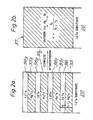
- Figures 2a, b are sectional views of a substrate during growth and after growth of CdxHg1-xTe material.
- As shown high purity hydrogen is supplied to a
hydrogen manifold 1 which maintains a supply for five mass-flow controllers Mass flow controller 2 supplies hydrogen via abypass line 14 to acombustion chamber 31 which burns exhaust vapour in a hydrogen flame.Mass flow controllers 3 and 4 supply hydrogen toalkyl bubblers 6, and 7, which respectively contain an alkyl of cadmium such as dimethyl cadmium and an alkyl of tellurium such as diethyl telluride. Hydrogen flow from thecontrollers 3 and 4 can be diverted viavalves bypass line 14 or throughvalves Valves bypass line 14. By control of flows throughcontrollers 3, 4, and 5, the concentrations of cadmium and tellurium alkyls in the mixed stream can be independently determined over a wide range of values. - The alkyl plus hydrogen mixture is passed into a
reactor vessel 16 which is heated with anelectrical resistance furnace 17 and R.F.induction coil 18. Inside the reactor vessel is amercury bath 19 and acarbon susceptor 21 carrying thesubstrate 20 to be coated with a layer of C.M.T. The furnace maintains the temperature of the reactor vessel wall from themercury reservoir 19 to thesubstrate 20 equal to or greater than the mercury reservoir temperature, the mercury reservoir being heated by thermal conduction through thereactor wall 24. The R.F.induction coil 18 couples into thecarbon susceptor 21 thereby heating the substrate to a temperature above that of thereactor wall 24 so that the cadmium and tellurium alkyls will crack and deposit cadmium and tellurium onto the surface of thesubstrate 20. The temperature of themercury reservoir 19 is determined by the requirement of the equilibrium partial pressure of mercury to be maintained at the growth interface. Thehot reactor wall 24 ensures that the mercury partial pressure in the vapour stream is the same at thesubstrate 20 as over themercury reservoir 19. - The walls of the
vessel 16 are sufficiently hot to prevent condensation of Hg without significant decomposition of the alkyls, whilst the temperature of thesubstrate 20 is sufficient to decompose the alkyls at thesubstrate 20 surface. The substrate may be inclined slightly e.g. 4° to give more uniform growth along the substrate. - A
water cooling jacket 22 at one end of thevessel 16 condenses out the unreacted mercury and prevents overheating of reactor vessel and plate seals. The exhaust vapour stream is then mixed with thebypass 14 stream of hydrogen and burnt in thecombustion chamber 31 for safety reasons. - A vacuum pump 30 is connected to the
vessel 16 via acold trap 29 for initial purging of thevessel 16. - To grow CMT on CdTe a cleaned
substrate 20 is placed on thesusceptor 21 in thevessel 16. Typical growth conditions are:vessel walls 16 andHg bath 19 temperatures 200-320°C (eg around 220 to 240°C); pressure inside the vessel around atmospheric; substrate temperature 400-430°C (eg around 410°C);alkyl bubbler 6, 7 temperature around 25°C. -
Valves 12, 13 are opened and 9 is closed to admit the Te alkyl together with H2 into thevessel 16. The Te and Hg combine and form a HgTe 35 (Figure 2) layer on the substrate. Typically a layer 0.16 pm thick is formed in less than one minute. -
Valves vessel 16, andvalve 33 closed andvalve 32 opened to add a dilution flow. The partial pressures of Cd and Te are arranged to be about equal. As a result the Cd alkyl combines preferentially with the Te alkyl in the region of thesubstrate 20 to form alayer 36 of CdTe. Typically a layer 0.04 Ilm thick is formed in less than one minute. - The combined thickness of the HgTe and CdTe layer is <0.5 µm thick, preferably <0.25 µm thick. Also the ratio of t2/(t, + t2) is arranged so that the value of x lies in the required range for example 0.2 or 0.3 for use in infra red detectors.
- Flow rate of gas through the
vessel 16 varies with the growing layer. Typically the flow rate during CdTe growth is 4 to 12 times that during HgTe growth. Typical flow rates for a 4 cm diameter vessel are 500 cc/min during HgTe growth and 4,000 cc/min during CdTe growth. - The
valves CdTe HgTe layer 37 of material CdxHg1-xTe (Figure 2b). Such diffusion is quite limited, typically to less than 1 µm. Thus the value of x can be changed during growth of many layers to give a device with a gradually changing composition (varying x) or one with sharp changes in the value of x. - The layer of C.M.T. grown on the substrate may include one or more dopants. Such a dopant is provided by passing hydrogen from the manifold through a
mass flow controller 23 to a bubbler 25 containing an alkyl of the dopant. Alternatively a volatile hydride of the dopant in hydrogen may be used. From the bubbler the alkyl passes to the mixer 15 and thence to thevessel 16.Valves - Examples of dopants and their alkyls are as follows:- Al, Ga, As, and P from the respective alkyls (CH3)3AI, (CH3)3Ga, (CH3)3As, (CH3)3P, (C2Hs)sAl, (C2H5)3Ga, (C2H5)3P.
- Examples of dopants and their hydrides are as follows: Si, Ge, As, and P from their respective hydrides SiH4, GeH4, AsH3 and PH3. A supply of the hydrides e.g. SiH4 may be supplied direct from gas cylinders.
- In another form of the apparatus (not shown) the
Cd compound supply 6 is connected via thevalve 11 direct into thevessel 16 at a distance from the Te compound entrance. A deflector is arranged inside the vessel and is movable to direct Cd either over or away from the substrate. This allows Cd, Te, and Hg to flow over the substrate, to grow CdTe; or for Te and Hg to flow over the substrate and grow HgTe. An advantage of this arrangement is that gas flow rates can remain constant whilst the two layers, CdTe, and HgTe are growing. - As an alternative to a movable deflector the substrate may be moved between two positions in the vessel. The first position is in a flow of Cd, Te and Hg whilst the second position is in a flow of Te and Hg gas.
- Using the above method and apparatus infra red detectors may be made. Such a detector may be a layer of C.M.T. on a CdTe substrate with a passivating layer of oxide or CdTe on the C.M.T. layer surface. The detector may be in the form of a strip with electrodes on the surface at each end as described in U.K. Patent Specification No. 1,488,258. Such a detector is photo conductive and has the image of a thermal scene scanned over its surface.
- Another type of I.R. detector uses a p-n junction e.g. the junction between two differently doped, p and n doped, C.M.T. layers to form a photo-voltaic detector. A voltage is applied by electrodes across the p-n junction and changes in current are a measure of the infra-red photons that are absorbed by the detector. Such a detector may be formed into a large array of I.R. detectors capable of imaging a thermal scene, without a scanning system, to form a so-called staring array system.
Claims (13)
Applications Claiming Priority (2)
| Application Number | Priority Date | Filing Date | Title |
|---|---|---|---|
| GB8324531 | 1983-09-13 | ||
| GB838324531A GB8324531D0 (en) | 1983-09-13 | 1983-09-13 | Cadmium mercury telluride |
Publications (2)
| Publication Number | Publication Date |
|---|---|
| EP0135344A1 EP0135344A1 (en) | 1985-03-27 |
| EP0135344B1 true EP0135344B1 (en) | 1987-10-21 |
Family
ID=10548729
Family Applications (1)
| Application Number | Title | Priority Date | Filing Date |
|---|---|---|---|
| EP84305396A Expired EP0135344B1 (en) | 1983-09-13 | 1984-08-08 | Manufacture of cadmium mercury telluride |
Country Status (7)
| Country | Link |
|---|---|
| US (1) | US4566918A (en) |
| EP (1) | EP0135344B1 (en) |
| JP (1) | JPH0650744B2 (en) |
| CA (1) | CA1229290A (en) |
| DE (1) | DE3466898D1 (en) |
| GB (2) | GB8324531D0 (en) |
| IL (1) | IL72790A (en) |
Families Citing this family (42)
| Publication number | Priority date | Publication date | Assignee | Title |
|---|---|---|---|---|
| GB8428032D0 (en) * | 1984-11-06 | 1984-12-12 | Secr Defence | Growth of crystalline layers |
| GB2177119B (en) * | 1985-06-26 | 1989-04-26 | Plessey Co Plc | Organometallic chemical vapour deposition |
| US4846926A (en) * | 1985-08-26 | 1989-07-11 | Ford Aerospace & Communications Corporation | HcCdTe epitaxially grown on crystalline support |
| US4743310A (en) * | 1985-08-26 | 1988-05-10 | Ford Aerospace & Communications Corporation | HGCDTE epitaxially grown on crystalline support |
| US4735910A (en) * | 1985-09-19 | 1988-04-05 | Matsushita Electric Industrial Co., Ltd. | In-situ doping of MBE grown II-VI compounds on a homo- or hetero-substrate |
| KR900002687B1 (en) * | 1985-12-16 | 1990-04-23 | 후지쓰가부시끼가이샤 | Method for growing 4-membered or 5-membered semiconducting semiconductors lattice matched to a substrate by MBE |
| JPH084072B2 (en) * | 1986-01-14 | 1996-01-17 | キヤノン株式会社 | Deposited film formation method |
| US4828938A (en) * | 1986-04-11 | 1989-05-09 | Hughes Aircraft Company | Method for depositing materials containing tellurium and product |
| US4946543A (en) * | 1986-06-02 | 1990-08-07 | Kalisher Murray H | Method and apparatus for growing films on a substrate |
| US4761269A (en) * | 1986-06-12 | 1988-08-02 | Crystal Specialties, Inc. | Apparatus for depositing material on a substrate |
| US4767494A (en) * | 1986-07-04 | 1988-08-30 | Nippon Telegraph & Telephone Corporation | Preparation process of compound semiconductor |
| US4719124A (en) * | 1986-07-28 | 1988-01-12 | American Telephone And Telegraph Company At&T Bell Laboratories | Low temperature deposition utilizing organometallic compounds |
| US4804638A (en) * | 1986-12-18 | 1989-02-14 | Raytheon Company | Metalorganic chemical vapor deposition growth of Group II-IV semiconductor materials having improved compositional uniformity |
| CA1319587C (en) * | 1986-12-18 | 1993-06-29 | William Hoke | Metalorganic chemical vapor depositing growth of group ii-vi semiconductor materials having improved compositional uniformity |
| GB2202236B (en) * | 1987-03-09 | 1991-04-24 | Philips Electronic Associated | Manufacture of electronic devices comprising cadmium mercury telluride |
| GB2203757B (en) * | 1987-04-16 | 1991-05-22 | Philips Electronic Associated | Electronic device manufacture |
| EP0305144A3 (en) * | 1987-08-24 | 1989-03-08 | Canon Kabushiki Kaisha | Method of forming crystalline compound semiconductor film |
| GB2211209A (en) * | 1987-10-16 | 1989-06-28 | Philips Electronic Associated | A method of forming a defect mixed oxide |
| US4901670A (en) * | 1988-08-22 | 1990-02-20 | Santa Barbara Research Center | Elemental mercury source for metal-organic chemical vapor deposition |
| US4935383A (en) * | 1988-09-23 | 1990-06-19 | The United States Of America As Represented By The Administrator Of The National Aeronautics And Space Administration | Preparation of dilute magnetic semiconductor films by metalorganic chemical vapor deposition |
| DE3918094A1 (en) * | 1989-06-02 | 1990-12-06 | Aixtron Gmbh | METHOD FOR PRODUCING DOPED SEMICONDUCTOR LAYERS |
| JP2754765B2 (en) * | 1989-07-19 | 1998-05-20 | 富士通株式会社 | Method for manufacturing compound semiconductor crystal |
| US5123995A (en) * | 1990-10-04 | 1992-06-23 | Aerodyne Research, Inc. | Low-temperature, photo-induced epitaxy |
| US5403760A (en) * | 1990-10-16 | 1995-04-04 | Texas Instruments Incorporated | Method of making a HgCdTe thin film transistor |
| US5202283A (en) * | 1991-02-19 | 1993-04-13 | Rockwell International Corporation | Technique for doping MOCVD grown crystalline materials using free radical transport of the dopant species |
| US5306660A (en) * | 1991-02-19 | 1994-04-26 | Rockwell International Corporation | Technique for doping mercury cadmium telluride MOCVD grown crystalline materials using free radical transport of elemental indium and apparatus therefor |
| IT1257434B (en) * | 1992-12-04 | 1996-01-17 | Cselt Centro Studi Lab Telecom | STEAM GENERATOR FOR VAPOR PHASE CHEMICAL LAYING PLANTS |
| JPH08255923A (en) * | 1995-03-15 | 1996-10-01 | Fujitsu Ltd | Semiconductor device using II-VI group compound semiconductor and manufacturing method thereof |
| US5998235A (en) * | 1997-06-26 | 1999-12-07 | Lockheed Martin Corporation | Method of fabrication for mercury-based quaternary alloys of infrared sensitive materials |
| GB9921639D0 (en) * | 1999-09-15 | 1999-11-17 | Secr Defence Brit | New organotellurium compound and new method for synthesising organotellurium compounds |
| US7041983B2 (en) * | 2001-10-12 | 2006-05-09 | Lockheed Martin Corporation | Planar geometry buried junction infrared detector and focal plane array |
| EP1953801B1 (en) * | 2002-06-10 | 2010-08-11 | eV Products, Inc. | Radiation detector |
| KR20050040969A (en) * | 2003-10-29 | 2005-05-04 | 삼성전자주식회사 | Diffusion system |
| GB0407804D0 (en) * | 2004-04-06 | 2004-05-12 | Qinetiq Ltd | Manufacture of cadmium mercury telluride |
| EP1784529B1 (en) * | 2004-08-02 | 2011-03-30 | Qinetiq Limited | Manufacture of cadmium mercury telluride on patterned silicon |
| US8371705B2 (en) * | 2008-03-11 | 2013-02-12 | The United States Of America As Represented By The Secretary Of The Army | Mirrors and methods of making same |
| CA2649322C (en) * | 2008-09-30 | 2011-02-01 | 5N Plus Inc. | Cadmium telluride production process |
| WO2010054231A1 (en) * | 2008-11-06 | 2010-05-14 | Arizona Board of Regents, a body corporate acting for and on behalf of Arizona State University | Laterally varying ii-vi alloys and uses thereof |
| FR2946184B1 (en) | 2009-05-27 | 2011-07-01 | Commissariat Energie Atomique | ENCLOSURE, DEVICE AND METHOD FOR RECLAIMING A TYPE II-VI SEMICONDUCTOR MATERIAL |
| JP5867856B2 (en) * | 2011-12-27 | 2016-02-24 | 株式会社フジクラ | Seed crystal holding member, aluminum nitride single crystal manufacturing method and manufacturing apparatus thereof |
| AU2018225659B2 (en) | 2017-02-24 | 2023-02-02 | First Solar, Inc. | Doped photovoltaic semiconductor layers and methods of making |
| CN117776121B (en) * | 2024-01-03 | 2025-07-04 | 电子科技大学 | Synthesis method of self-aggregation growth monodisperse HgTe quantum dot |
Family Cites Families (12)
| Publication number | Priority date | Publication date | Assignee | Title |
|---|---|---|---|---|
| US3218203A (en) * | 1961-10-09 | 1965-11-16 | Monsanto Co | Altering proportions in vapor deposition process to form a mixed crystal graded energy gap |
| US3312571A (en) * | 1961-10-09 | 1967-04-04 | Monsanto Co | Production of epitaxial films |
| US3619283A (en) * | 1968-09-27 | 1971-11-09 | Ibm | Method for epitaxially growing thin films |
| US3725135A (en) * | 1968-10-09 | 1973-04-03 | Honeywell Inc | PROCESS FOR PREPARING EPITAXIAL LAYERS OF Hg{11 {118 {11 Cd{11 Te |
| US3664866A (en) * | 1970-04-08 | 1972-05-23 | North American Rockwell | Composite, method for growth of ii{11 {14 vi{11 {0 compounds on substrates, and process for making composition for the compounds |
| US3622405A (en) * | 1970-06-22 | 1971-11-23 | Honeywell Inc | Method for reducing compositional gradients in{11 {11 {11 {11 {11 {11 {11 {11 {11 {11 |
| GB2055774B (en) * | 1979-04-09 | 1983-02-02 | Plessey Co Ltd | Methods of producing semiconductor materials |
| FR2484469A1 (en) * | 1980-02-22 | 1981-12-18 | Telecommunications Sa | PROCESS FOR THE PREPARATION OF HOMOGENEOUS LAYERS OF HG1-XCDXTE |
| GB2078695B (en) * | 1980-05-27 | 1984-06-20 | Secr Defence | Cadmium mercury telluride deposition |
| LU82690A1 (en) * | 1980-08-05 | 1982-05-10 | Lucien D Laude | PROCESS FOR THE PREPARATION OF COMPOUND OR ELEMENTARY SEMICONDUCTOR POLYCRYSTALLINE FILMS AND FILMS OBTAINED THEREBY |
| DE3278553D1 (en) * | 1981-06-24 | 1988-06-30 | Secr Defence Brit | Photo diodes |
| US4439267A (en) * | 1982-09-29 | 1984-03-27 | The United States Of America As Represented By The Secretary Of The Army | Vapor-phase method for growing mercury cadmium telluride |
-
1983
- 1983-09-13 GB GB838324531A patent/GB8324531D0/en active Pending
-
1984
- 1984-08-08 DE DE8484305396T patent/DE3466898D1/en not_active Expired
- 1984-08-08 EP EP84305396A patent/EP0135344B1/en not_active Expired
- 1984-08-16 US US06/641,483 patent/US4566918A/en not_active Expired - Lifetime
- 1984-08-28 IL IL72790A patent/IL72790A/en not_active IP Right Cessation
- 1984-09-10 JP JP59189463A patent/JPH0650744B2/en not_active Expired - Fee Related
- 1984-09-10 GB GB08422817A patent/GB2146663B/en not_active Expired
- 1984-09-10 CA CA000462750A patent/CA1229290A/en not_active Expired
Also Published As
| Publication number | Publication date |
|---|---|
| JPH0650744B2 (en) | 1994-06-29 |
| JPS6077431A (en) | 1985-05-02 |
| DE3466898D1 (en) | 1987-11-26 |
| US4566918A (en) | 1986-01-28 |
| GB8422817D0 (en) | 1984-10-17 |
| IL72790A (en) | 1988-01-31 |
| CA1229290A (en) | 1987-11-17 |
| GB2146663A (en) | 1985-04-24 |
| GB2146663B (en) | 1986-11-26 |
| GB8324531D0 (en) | 1983-10-12 |
| EP0135344A1 (en) | 1985-03-27 |
Similar Documents
| Publication | Publication Date | Title |
|---|---|---|
| US4566918A (en) | Utilizing interdiffusion of sequentially deposited links of HgTe and CdTe | |
| US4650539A (en) | Manufacture of cadmium mercury telluride | |
| US4066481A (en) | Metalorganic chemical vapor deposition of IVA-IVA compounds and composite | |
| US4404265A (en) | Epitaxial composite and method of making | |
| US4568397A (en) | Metalorganic vapor phase epitaxial growth of group II-VI semiconductor materials | |
| EP0200766B1 (en) | Method of growing crystalline layers by vapour phase epitaxy | |
| JP3879173B2 (en) | Compound semiconductor vapor deposition method | |
| US3933538A (en) | Method and apparatus for production of liquid phase epitaxial layers of semiconductors | |
| CA1270424A (en) | Chemical beam deposition method | |
| GB2163000A (en) | Apparatus for forming crystal of semiconductor | |
| Tsang | Chemical beam epitaxy of InGaAs | |
| US5432121A (en) | Method for fabricating a multilayer epitaxial structure | |
| KR101110592B1 (en) | Manufacture of cadmium mercury telluride | |
| US4439267A (en) | Vapor-phase method for growing mercury cadmium telluride | |
| US4886683A (en) | Low temperature metalorganic chemical vapor depostion growth of group II-VI semiconductor materials | |
| US4470192A (en) | Method of selected area doping of compound semiconductors | |
| GB2078695A (en) | Cadmium Mercury Telluride Deposition | |
| Beneking et al. | Characterization of GaAs epitaxial layers grown in a radiation heated Mo-CVD reactor | |
| US3839082A (en) | Epitaxial growth process for iii-v mixed-compound semiconductor crystals | |
| Besomi et al. | Growth and characterization of heteroepitaxial zinc selenide | |
| US4115164A (en) | Method of epitaxial deposition of an AIII BV -semiconductor layer on a germanium substrate | |
| Herman et al. | Molecular beam epitaxy | |
| US5229319A (en) | Method for producing compound semiconductors and apparatus therefor | |
| König et al. | Contact Angles Between III–V Melts and Several Substrates | |
| US5324685A (en) | Method for fabricating a multilayer epitaxial structure |
Legal Events
| Date | Code | Title | Description |
|---|---|---|---|
| PUAI | Public reference made under article 153(3) epc to a published international application that has entered the european phase |
Free format text: ORIGINAL CODE: 0009012 |
|
| AK | Designated contracting states |
Designated state(s): DE FR IT NL |
|
| 17P | Request for examination filed |
Effective date: 19850816 |
|
| 17Q | First examination report despatched |
Effective date: 19860515 |
|
| ITF | It: translation for a ep patent filed | ||
| GRAA | (expected) grant |
Free format text: ORIGINAL CODE: 0009210 |
|
| AK | Designated contracting states |
Kind code of ref document: B1 Designated state(s): DE FR IT NL |
|
| REF | Corresponds to: |
Ref document number: 3466898 Country of ref document: DE Date of ref document: 19871126 |
|
| ET | Fr: translation filed | ||
| PLBE | No opposition filed within time limit |
Free format text: ORIGINAL CODE: 0009261 |
|
| STAA | Information on the status of an ep patent application or granted ep patent |
Free format text: STATUS: NO OPPOSITION FILED WITHIN TIME LIMIT |
|
| 26N | No opposition filed | ||
| ITTA | It: last paid annual fee | ||
| PGFP | Annual fee paid to national office [announced via postgrant information from national office to epo] |
Ref country code: FR Payment date: 20020708 Year of fee payment: 19 |
|
| REG | Reference to a national code |
Ref country code: FR Ref legal event code: TP |
|
| PGFP | Annual fee paid to national office [announced via postgrant information from national office to epo] |
Ref country code: NL Payment date: 20020715 Year of fee payment: 19 |
|
| PGFP | Annual fee paid to national office [announced via postgrant information from national office to epo] |
Ref country code: DE Payment date: 20020724 Year of fee payment: 19 |
|
| NLS | Nl: assignments of ep-patents |
Owner name: QINETIQ LIMITED |
|
| PG25 | Lapsed in a contracting state [announced via postgrant information from national office to epo] |
Ref country code: NL Free format text: LAPSE BECAUSE OF NON-PAYMENT OF DUE FEES Effective date: 20040301 |
|
| PG25 | Lapsed in a contracting state [announced via postgrant information from national office to epo] |
Ref country code: DE Free format text: LAPSE BECAUSE OF NON-PAYMENT OF DUE FEES Effective date: 20040302 |
|
| PG25 | Lapsed in a contracting state [announced via postgrant information from national office to epo] |
Ref country code: FR Free format text: LAPSE BECAUSE OF NON-PAYMENT OF DUE FEES Effective date: 20040430 |
|
| NLV4 | Nl: lapsed or anulled due to non-payment of the annual fee |
Effective date: 20040301 |
|
| REG | Reference to a national code |
Ref country code: FR Ref legal event code: ST |