EP0131024B1 - Capacitance measuring circuit - Google Patents
Capacitance measuring circuit Download PDFInfo
- Publication number
- EP0131024B1 EP0131024B1 EP19840900387 EP84900387A EP0131024B1 EP 0131024 B1 EP0131024 B1 EP 0131024B1 EP 19840900387 EP19840900387 EP 19840900387 EP 84900387 A EP84900387 A EP 84900387A EP 0131024 B1 EP0131024 B1 EP 0131024B1
- Authority
- EP
- European Patent Office
- Prior art keywords
- capacitance
- measuring circuit
- output
- capacitance measuring
- current
- Prior art date
- Legal status (The legal status is an assumption and is not a legal conclusion. Google has not performed a legal analysis and makes no representation as to the accuracy of the status listed.)
- Expired
Links
Images


Classifications
-
- G—PHYSICS
- G01—MEASURING; TESTING
- G01R—MEASURING ELECTRIC VARIABLES; MEASURING MAGNETIC VARIABLES
- G01R27/00—Arrangements for measuring resistance, reactance, impedance, or electric characteristics derived therefrom
- G01R27/02—Measuring real or complex resistance, reactance, impedance, or other two-pole characteristics derived therefrom, e.g. time constant
- G01R27/26—Measuring inductance or capacitance; Measuring quality factor, e.g. by using the resonance method; Measuring loss factor; Measuring dielectric constants ; Measuring impedance or related variables
- G01R27/2605—Measuring capacitance
Definitions
- the invention relates to a capacitance measuring circuit comprising an oscillator circuit, where the capacitance to be measured forms a link of a series connected frequency-determining set of impedances, which is connected to the oscillator circuit only at the end terminals of the series connection, in the following referred to as the first end terminal and the second end terminal.
- a constant voltage is applied to the frequency-determining series connected impedances, and the frequency is determined by measurement of the charging current of the capacitance, as contrasted to the known capacitance measuring circuits in which a constant current is applied to the frequency-determining series connected impedances, and the frequency is determined by measurement of the voltage.
- this capacitance measuring circuit cannot function with the most widespread group of capacitive transducers, viz. those having one terminal grounded.
- one end terminal G of the series connected frequency-determining impedances R T C T is connected to a fixed voltage, while their other end terminal H is connected to the inverting input 2 of an operational amplifier A, said input being also connected to the output 6 of the operational amplifier through a resistor R s .
- the non-inverting input of a comparator K is connected to the output 6 of the operational amplifier, and the inverting input of the comparator is connected to a reference voltage which has the constant positive value U REF + and the constant negative value U REF ⁇ in the positive and the negative half-cycle respectively.
- the output 7 of the comparator which can only assume either the positive maximum voltage U K + or the negative maximum voltage Ur-, cf. the graph of Fig. 2, is connected to the non-inverting input 3 of the operational amplifier.
- CO symbolizes the sum of the stray and input capacitances of the inverting input 2 of the operational amplifier.
- the output 6 consequently assumes a positive voltage which through the resistor R s will raise the voltage on the input 2, and thereby the voltage across the series connection of R T R T , to the constant voltage U K +.
- the output 6 will assume a negative voltage which through the resistor R s will lower the voltage on input 2 and thereby on the series connection R T C T to the constant voltage U K ⁇ .
- This charging has been effected by the superposition of a current J co of very short duration on the current J RC .
- This current does not in any way affect the charging current J RC , which is only determined by C T and the constant voltage U K and R T , and seeing that, even in the case of great values of C0, the current J co has dropped to 0 long before the charging current J RC reaches its shifting value, it will be seen that the charging of C0, and thereby the size of C0, has no influence on the frequency of this measuring circuit according to the invention.
- the oscillator circuit of Fig. 4 comprises a buffer amplifier B with the voltage supplies U B + and U B -.
- the buffer amplifier has the job of driving the terminal 3 of the operational amplifier A and possibly also of driving the associated frequency measuring equipment.
- the comparator voltage U K has now been replaced by the buffer voltage U B and is, like before, connected to the input 3 of the operational amplifier A, and is also used as reference for the comparator K.
- the resistor R 3 has been provided in order to establish a positive feed-back in the comparator, in a manner known per se, so as to make the comparator change over quickly even if the voltage change on the non-inverting input is relatively slow.
- the voltage supply Up+ and Up- to the operational amplifier is so connected as to be bootstrapped with the input 3, when this is changed over between U B + and U B ⁇ .
- an inverting amplifier A' is inserted between the operational amplifier A and the Schmitt-trigger S, where the amplification is determined by the proportion of R 4 to R 5 .
- FIG. 8 Another method of avoiding subdivision of the voltage U A and still making the input voltage of the comparator pass the reference voltage during the discharging of C r is shown in Fig. 8, where the resistor R 6 provides a constant positive and a constant negative current into the frequency-determining series connected impedances in the positive and the negative half-cycle, respectively.
- Fig. 8 also shows two diodes D connected in anti-parallel and serving to obtain the fastest possible charging of the stray and input capacitances on input 2 of the amplifier A. This is of importance when these capacitances assume very high values so that a charging through R s alone will be too slow.
- These diodes can of course also be used in the other capacitance measuring circuits according to the invention shown in the drawing.
- the series connected frequency-determining impedances may in principle be RC, LC or RCL combinations or mechanical resonators.
- An advantage can also be obtained by connect. ing series connected reference impedance sets, having a fixed, known value, to a capacitance measuring circuit according to the invention in succession with the subject impedance sets.
- These reference impedance sets may deliver signals which can be utilized for the complete correction for drifting in the components common to a plurality of measurements, and for producing fault indication signals, if as a consequence of faults the signal frequencies from one or more subject impedance sets go beyond certain tolerances relatively to the reference frequencies.
- reference impedance sets also makes it possible to perform an accurate absolute measurement of capacitances.
- the measuring circuit may be particularly .
- the other end of R T may, owing to the advantageous properties of the capacitance measuring circuit, be connected to this circuit through a relatively long conductor, such as is in practice frequently desirable.
- the measuring circuit according to the invention can in a simple manner provide a stable and linear measuring result which is accurately representative of the subjet capacitance.
Abstract
Description
- The invention relates to a capacitance measuring circuit comprising an oscillator circuit, where the capacitance to be measured forms a link of a series connected frequency-determining set of impedances, which is connected to the oscillator circuit only at the end terminals of the series connection, in the following referred to as the first end terminal and the second end terminal.
- From DE-PS 2 712 369 C2 and from the periodical " Industriel Teknik 3-1974. page 27, capacitance measuring oscillator circuits of the kind referred to are known in which a constant current is applied to the series connected set of impedances. In these circuits the voltage across the series connection varies continuously during each half-cycle, and the charge on the stray and input capacitances of the voltage detector will therefore vary during the whole of the half-cycle. This charge is to be delivered by a constant current generator belonging to the circuit, and the charging of the subject capacitance, and thereby the oscillator frequency, will therefore depend on changes of the size of the stray and input capacitances.
- It is the object of the invention to devise an oscillator circuit of the kind referred to in such a manner as to be capable of measuring capacitances without undesired influence of stray and input capacitances, whereby a high stability and linearity of the measurement can be obtained.
- This is achieved, according to the invention, by so arranging the circuit that the first end terminal is connected to a constant voltage, while the second end terminal is connected to a point of the oscillator circuit where that circuit maintains a constant voltage during each half-cycle, while at the same time sensing the charging current flowing into the capacitance so as to be triggered at the moment when the charging current thus sensed has dropped to a predetermined value.
- It will be seen that when the voltage across the series connection is maintained constant in each half-cycle, the charge on the stray and input capacitances is likewise constant in each half-cycle, and since the recharging of the stray and input capacitances to the constant voltage takes place at the start of each half-cycle, the size of this constant charge and thereby the size of the stray and input capacitances has no influence on the subsequent charging of the subject capacitance and consequently no influence on the frequency of the oscillator circuit, which is representative of the value of the subject capacitance.
- Thus, it is a distinguishing feature of the measuring circuit according to the invention that a constant voltage is applied to the frequency-determining series connected impedances, and the frequency is determined by measurement of the charging current of the capacitance, as contrasted to the known capacitance measuring circuits in which a constant current is applied to the frequency-determining series connected impedances, and the frequency is determined by measurement of the voltage.
- From GB 2.006.442 A a capacitance measuring circuit is known in which the influence of the stray capacitances has been reduced by including the subject capacitance in an integrator connected to a Schmitt-trigger.
- Here the series connection of the frequency-determining impedances is not connected to the measuring circuit at its end terminals only, but both terminals of the subject capacitance are connected directly to the output and the inverting input of the amplifier.
- Hereby the stray capacitances to ground are in fact eliminated, but the coupling capacitance between the input and the output of the amplifier, which is frequently substantial, is in this case connected directly in parallel to the subject capacitance.
- Since this coupling capacitance depends on many parameters, such as temperature, amplification, voltage supply etc., it will have an appreciable influence on the accuracy of measurement.
- Besides, this capacitance measuring circuit cannot function with the most widespread group of capacitive transducers, viz. those having one terminal grounded.
- The invention will now be described in further detail with reference to the drawing, in which
- Figure 1 shows a particularly advantageous embodiment of the invention, in which the current-sensing, constant-voltage-maintaining circuit consists of an inverting operational amplifier in conjuction with a comparator,
- Figure 2 a graph of the output voltage UK of the comparator of Fig. 1,
- Figure 3 a graph of the output voltage UA of the operational amplifier of Fig. 1,
- Figure 4 shows a capacitance measuring circuit according to the invention, illustrating a method of establishing the reference voltage for the comparator,
- Figure 5 shows a capacitance measuring circuit according to the invention in which an inverting amplifier is inserted between the current-sensing operational amplifier and the comparator.
- Figure 6 a graph of the output voltages UA1 of the inverting amplifier of Fig. 5,
- Figure 7 a graph of the output voltage UA of the comparator of Fig. 5,
- Figure 8 a capacitance measuring circuit according to the invention in which the charging current for the series connected frequency-determining impedances is superposed on a constant current,
- Figure 9 a capacitance measuring circuit according to the invention with alternative switching of a plurality of series connected frequency-determining sets of impedances to the same current-sensing operational amplifier, and
- Figure 10 a capacitance measuring circuit according - to the invention with alternative switching of a plurality of current-sensing operational amplifiers to the same comparator and buffer.
- In the capacitance measuring circuit of Fig. 1 one end terminal G of the series connected frequency-determining impedances RTCT is connected to a fixed voltage, while their other end terminal H is connected to the inverting
input 2 of an operational amplifier A, said input being also connected to theoutput 6 of the operational amplifier through a resistor Rs. The non-inverting input of a comparator K is connected to theoutput 6 of the operational amplifier, and the inverting input of the comparator is connected to a reference voltage which has the constant positive value UREF+ and the constant negative value UREF― in the positive and the negative half-cycle respectively. - The
output 7 of the comparator, which can only assume either the positive maximum voltage UK+ or the negative maximum voltage Ur-, cf. the graph of Fig. 2, is connected to thenon-inverting input 3 of the operational amplifier. - CO symbolizes the sum of the stray and input capacitances of the inverting
input 2 of the operational amplifier. - Assuming the operational amplifier to be ideal, meaning in the present context that no current flows into the
inputs input 2 to assume exactly the same voltage as that applied to theinput 3, the function of this capacitance measuring circuit is a follows: - At the time T1, UK is assumed to have its positive maximum value UK+, which is also applied to the
input 3 of the operational amplifier A. - The
output 6 consequently assumes a positive voltage which through the resistor Rs will raise the voltage on theinput 2, and thereby the voltage across the series connection of RTRT, to the constant voltage UK+. - This positive voltage change across the series connection will cause a current JRc to flow into RTCT.
- Since no current flows into the
input 2, the said current must be delivered via Rs, and the output voltage UA of the comparator must therefore assume the value UA = UK + + RS JRC. - The current JRC drops exponentially, and thereby UA drops, and when suitably selecting the constant value UREF+, which can advantageously be made proportional to UK+, UA will pass UREF+, and the output of the comparator will shift to its negative maximum value UK―, which is now applied to the
input 3 of the operational amplifier, cf. the graph of Fig. 3. - As a consequence, the
output 6 will assume a negative voltage which through the resistor Rs will lower the voltage oninput 2 and thereby on the series connection RTCT to the constant voltage UK―. - This negative voltage change on the series connection RTCT will cause a current JRC to flow out of RTCT, and, like before, this current must be delivered via Rs, and the output voltage UA will therefore assume the value UA = UK - RSJRC.
- Like before, the current drops exponentially, whereby UA drops, and when suitably selecting the reference voltage, which now has the constant negative value UREF―, UA will pass UREr-, and the output of the comparator will be shifted to its positive maximum value UK+, which is again applied to the
input 3. In this manner the oscillations continue at a frequency F determined by the time constant RTCT in conjuction with the resistor Rs, the charging voltages UK+ and UK― and the reference voltages UREF+ and UREF―, which with modern components can all be made very stable. - Owing to the fact that the operational amplifier, through the resistor Rs, has almost instantly upon the change-over imposed upon its inverting
input 2 the same voltage UK as that applied to theinput 3 from the comparator, the stray capacitance CO has of course just as promptly been charged to the same constant voltage. - This charging has been effected by the superposition of a current Jco of very short duration on the current JRC.
- This current does not in any way affect the charging current JRC, which is only determined by CT and the constant voltage UK and RT, and seeing that, even in the case of great values of C0, the current Jco has dropped to 0 long before the charging current JRC reaches its shifting value, it will be seen that the charging of C0, and thereby the size of C0, has no influence on the frequency of this measuring circuit according to the invention.
- The oscillator circuit of Fig. 4 comprises a buffer amplifier B with the voltage supplies UB+ and UB-.
- The buffer amplifier has the job of driving the
terminal 3 of the operational amplifier A and possibly also of driving the associated frequency measuring equipment. - The comparator voltage UK has now been replaced by the buffer voltage UB and is, like before, connected to the
input 3 of the operational amplifier A, and is also used as reference for the comparator K. - Since the output voltage of the operational amplifier is UA = UB + RSJRC, it will be seen that if UA is directly applied to the non-inverting input of the comparator, the inputs of the comparator will assume the same voltage only when JRC = 0, i. e. the comparator will not change over.
- Therefore, a suitable voltage division of UA is established by means of the resistors R1, R2 and R4, whereby the voltage on the input of the comparator will pass the reference UB when JRC has dropped to a suitable value.
- The resistor R3 has been provided in order to establish a positive feed-back in the comparator, in a manner known per se, so as to make the comparator change over quickly even if the voltage change on the non-inverting input is relatively slow.
- The voltage supply Up+ and Up- to the operational amplifier is so connected as to be bootstrapped with the
input 3, when this is changed over between UB+ and UB―. - By this arrangement the advantage is obtained that the voltage on the output of the operational amplifier changes over more quickly since also the output follows Up+. Up― and the
input 3 when the buffer changes over between UB+ and UB―, and the operational amplifier therefore only has to contribute the voltage shift RSJRC. Besides, the advantage is obtained that common mode errors in the operational amplifier are avoided. - In the capacitance measuring circuit of Fig. 5, an inverting amplifier A' is inserted between the operational amplifier A and the Schmitt-trigger S, where the amplification is determined by the proportion of R4 to R5.
- Since the voltage supply Up+, Up- for both A and A' is bootstrapped with the output voltage of the Schmitt-trigger and thereby with the voltage on the
input 3 of A, the graph of the output voltages UA and UA1 will be as shown in Figs. 6 and 7. - It will be seen that the graph of UA1 passes the
value 0 at dropping current JRC, and for this reason the comparator can be replaced by the Schmitt-trigger S which acts as a comparator with hysteresis and thereference voltage 0, - By this measuring circuit according to the invention the further advantage is obtained that the voltage supplied to the Schmitt-trig- ger/comparator is amplified.
- Another method of avoiding subdivision of the voltage UA and still making the input voltage of the comparator pass the reference voltage during the discharging of Cr is shown in Fig. 8, where the resistor R6 provides a constant positive and a constant negative current into the frequency-determining series connected impedances in the positive and the negative half-cycle, respectively.
- When this current exceeds JRC, the output voltage UA will shift in relation to the voltage on the
input 3 of the operational amplifier and thereby in relation to the reference voltage of the comparator, which is determined by voltage division between R7 and Re. - Fig. 8 also shows two diodes D connected in anti-parallel and serving to obtain the fastest possible charging of the stray and input capacitances on
input 2 of the amplifier A. This is of importance when these capacitances assume very high values so that a charging through Rs alone will be too slow. These diodes can of course also be used in the other capacitance measuring circuits according to the invention shown in the drawing. - In the use of the capacitance measuring circuit according to the invention it is possible, as illustrated in Fig. 9, in a simple manner to connect a plurality of sets of series connected frequency- determined impedances RT" CT1-RTN.CTN successively to the same current-sensing operational amplifier, seeing that, as explained above, the stray capacitances from supply conductors and switches have no influence on the frequencies F1-FN.
- Hereby a succession of frequencies is obtained, which by suitable calculation, e. g. in a computer connected to the circuit, can be used for determining a function of the various capacitances CT1-CTN and to eliminate drifting and ageing of the components common to a plurality of measurements, such as the amplifier A, the comparator K and the resistors R1, R2, R3 and R4.
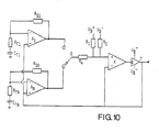
- At high temperatures leakage currents from the switches in Fig. 9 may, however, affect the charging of the subject capacitances, and it may then be advantageous to connect two or more current-sensing operational amplifiers A1-AN through a
switch 0 to a common comparator K and buffer B, as shown in Fig. 10. - In the capacitance measuring circuit according to the invention, the series connected frequency-determining impedances may in principle be RC, LC or RCL combinations or mechanical resonators.
- However, a great advantage is obtained by using a RC-oscillator, because the frequency of this is proportional to the electrode spacing of a capacitive transducer. This is, however, only the case when the influence from the stray and input capacitances can be eliminated, such as has been achieved by the present invention.
- An advantage can also be obtained by connect. ing series connected reference impedance sets, having a fixed, known value, to a capacitance measuring circuit according to the invention in succession with the subject impedance sets. These reference impedance sets may deliver signals which can be utilized for the complete correction for drifting in the components common to a plurality of measurements, and for producing fault indication signals, if as a consequence of faults the signal frequencies from one or more subject impedance sets go beyond certain tolerances relatively to the reference frequencies.
- The use of reference impedance sets also makes it possible to perform an accurate absolute measurement of capacitances.
- In the practical use of the measuring circuit according to the invention it may be particularly . advantageous to arrange the resistor RT with one supply terminal directly on the capacitor electrode of a capacitive transducer, whereby stray capacitances in the point of junction of the series connection are totally avoided.
- The other end of RT may, owing to the advantageous properties of the capacitance measuring circuit, be connected to this circuit through a relatively long conductor, such as is in practice frequently desirable.
- As will be seen, the measuring circuit according to the invention can in a simple manner provide a stable and linear measuring result which is accurately representative of the subjet capacitance.
Claims (9)
Priority Applications (1)
| Application Number | Priority Date | Filing Date | Title |
|---|---|---|---|
| AT84900387T ATE22620T1 (en) | 1983-01-07 | 1984-01-06 | CAPACITANCE MEASUREMENT CIRCUIT. |
Applications Claiming Priority (2)
| Application Number | Priority Date | Filing Date | Title |
|---|---|---|---|
| DK4383A DK4383A (en) | 1983-01-07 | 1983-01-07 | oscillator circuit |
| DK43/83 | 1983-01-07 |
Publications (2)
| Publication Number | Publication Date |
|---|---|
| EP0131024A1 EP0131024A1 (en) | 1985-01-16 |
| EP0131024B1 true EP0131024B1 (en) | 1986-10-01 |
Family
ID=8089086
Family Applications (1)
| Application Number | Title | Priority Date | Filing Date |
|---|---|---|---|
| EP19840900387 Expired EP0131024B1 (en) | 1983-01-07 | 1984-01-06 | Capacitance measuring circuit |
Country Status (4)
| Country | Link |
|---|---|
| EP (1) | EP0131024B1 (en) |
| DE (1) | DE3460831D1 (en) |
| DK (1) | DK4383A (en) |
| WO (1) | WO1984002780A1 (en) |
Cited By (4)
| Publication number | Priority date | Publication date | Assignee | Title |
|---|---|---|---|---|
| US7343814B2 (en) | 2006-04-03 | 2008-03-18 | Loadstar Sensors, Inc. | Multi-zone capacitive force sensing device and methods |
| US7353713B2 (en) | 2003-04-09 | 2008-04-08 | Loadstar Sensors, Inc. | Flexible apparatus and method to enhance capacitive force sensing |
| US7451659B2 (en) | 2004-09-29 | 2008-11-18 | Loadstar Sensors, Inc. | Gap-change sensing through capacitive techniques |
| US7570065B2 (en) | 2006-03-01 | 2009-08-04 | Loadstar Sensors Inc | Cylindrical capacitive force sensing device and method |
Families Citing this family (3)
| Publication number | Priority date | Publication date | Assignee | Title |
|---|---|---|---|---|
| US4918376A (en) * | 1989-03-07 | 1990-04-17 | Ade Corporation | A.C. capacitive gauging system |
| DE102011004645A1 (en) | 2011-02-24 | 2012-08-30 | Siemens Aktiengesellschaft | Circuit arrangement for measuring a capacitance, and use of such a circuit arrangement |
| DE102012216553A1 (en) | 2012-09-17 | 2014-03-20 | Siemens Aktiengesellschaft | Method for current measurement in primary conductor for e.g. long overhead lines for distributing electrical energy, involves adjusting compensation current based on regulating signal, and determining current based on adjusted current |
Family Cites Families (3)
| Publication number | Priority date | Publication date | Assignee | Title |
|---|---|---|---|---|
| US3581196A (en) * | 1968-10-28 | 1971-05-25 | William L Spaid | Digital capacitance meter by measuring capacitor discharge time |
| DE2712369C2 (en) * | 1977-03-22 | 1981-09-24 | Licentia Patent-Verwaltungs-Gmbh, 6000 Frankfurt | Oscillator for generating square-wave pulses |
| FI57319C (en) * | 1977-10-14 | 1980-07-10 | Vaisala Oy | ADJUSTMENT OF CAPACITY IN CAPACITY |
-
1983
- 1983-01-07 DK DK4383A patent/DK4383A/en not_active Application Discontinuation
-
1984
- 1984-01-06 EP EP19840900387 patent/EP0131024B1/en not_active Expired
- 1984-01-06 WO PCT/DK1984/000002 patent/WO1984002780A1/en active IP Right Grant
- 1984-01-06 DE DE8484900387T patent/DE3460831D1/en not_active Expired
Cited By (4)
| Publication number | Priority date | Publication date | Assignee | Title |
|---|---|---|---|---|
| US7353713B2 (en) | 2003-04-09 | 2008-04-08 | Loadstar Sensors, Inc. | Flexible apparatus and method to enhance capacitive force sensing |
| US7451659B2 (en) | 2004-09-29 | 2008-11-18 | Loadstar Sensors, Inc. | Gap-change sensing through capacitive techniques |
| US7570065B2 (en) | 2006-03-01 | 2009-08-04 | Loadstar Sensors Inc | Cylindrical capacitive force sensing device and method |
| US7343814B2 (en) | 2006-04-03 | 2008-03-18 | Loadstar Sensors, Inc. | Multi-zone capacitive force sensing device and methods |
Also Published As
| Publication number | Publication date |
|---|---|
| DK4383A (en) | 1984-07-08 |
| DK4383D0 (en) | 1983-01-07 |
| DE3460831D1 (en) | 1986-11-06 |
| WO1984002780A1 (en) | 1984-07-19 |
| EP0131024A1 (en) | 1985-01-16 |
Similar Documents
| Publication | Publication Date | Title |
|---|---|---|
| US4216424A (en) | Method and apparatus for testing electrolytic capacitors | |
| JPS6237440B1 (en) | ||
| US4820991A (en) | Apparatus for determination of the location of a fault in communications wires | |
| US4737706A (en) | Capacitance measuring circuit | |
| EP0131024B1 (en) | Capacitance measuring circuit | |
| US3783374A (en) | Capacitance difference detector circuit | |
| US4797603A (en) | Device for measuring the ratio of two low value capacities | |
| US4272718A (en) | Moisture meter | |
| US4011503A (en) | Apparatus for measuring the phase relation of two alternating current signals | |
| US3024658A (en) | Measuring system | |
| EP0135214B1 (en) | Apparatus for measuring a temperature | |
| US3541462A (en) | Apparatus for measuring low voltages and currents with amplifier protective means | |
| US3448378A (en) | Impedance measuring instrument having a voltage divider comprising a pair of amplifiers | |
| US3577072A (en) | Bridge circuit for differentially measuring capacitance | |
| EP1386173B1 (en) | Capacitance measuring circuit | |
| US4022990A (en) | Technique and apparatus for measuring the value of a capacitance in an electrical circuit such as a telephone communication line | |
| GB944385A (en) | Improvements in and relating to apparatus and methods for testing transistors | |
| US2523399A (en) | Null-balance frequency meter | |
| KR100516796B1 (en) | Current detection circuit of a/f sensor | |
| US3224275A (en) | Control apparatus | |
| US2929986A (en) | Apparatus for impedance measurements | |
| US3076129A (en) | Millivolt inverter | |
| US2820194A (en) | Apparatus for measuring electrical characteristics | |
| US4050018A (en) | Capacitance meter bias protection circuit | |
| US2501769A (en) | Vacuum tube voltmeter with balanced input shunt diode |
Legal Events
| Date | Code | Title | Description |
|---|---|---|---|
| PUAI | Public reference made under article 153(3) epc to a published international application that has entered the european phase |
Free format text: ORIGINAL CODE: 0009012 |
|
| 17P | Request for examination filed |
Effective date: 19840831 |
|
| AK | Designated contracting states |
Designated state(s): AT BE CH DE FR GB LI LU NL SE |
|
| GRAA | (expected) grant |
Free format text: ORIGINAL CODE: 0009210 |
|
| AK | Designated contracting states |
Kind code of ref document: B1 Designated state(s): AT BE CH DE FR GB LI LU NL SE |
|
| PG25 | Lapsed in a contracting state [announced via postgrant information from national office to epo] |
Ref country code: AT Effective date: 19861001 |
|
| REF | Corresponds to: |
Ref document number: 22620 Country of ref document: AT Date of ref document: 19861015 Kind code of ref document: T |
|
| REF | Corresponds to: |
Ref document number: 3460831 Country of ref document: DE Date of ref document: 19861106 |
|
| ET | Fr: translation filed | ||
| PLBE | No opposition filed within time limit |
Free format text: ORIGINAL CODE: 0009261 |
|
| STAA | Information on the status of an ep patent application or granted ep patent |
Free format text: STATUS: NO OPPOSITION FILED WITHIN TIME LIMIT |
|
| 26N | No opposition filed | ||
| EPTA | Lu: last paid annual fee | ||
| EAL | Se: european patent in force in sweden |
Ref document number: 84900387.6 |
|
| PGFP | Annual fee paid to national office [announced via postgrant information from national office to epo] |
Ref country code: GB Payment date: 20001220 Year of fee payment: 18 |
|
| PGFP | Annual fee paid to national office [announced via postgrant information from national office to epo] |
Ref country code: SE Payment date: 20010109 Year of fee payment: 18 |
|
| PGFP | Annual fee paid to national office [announced via postgrant information from national office to epo] |
Ref country code: FR Payment date: 20010112 Year of fee payment: 18 |
|
| PGFP | Annual fee paid to national office [announced via postgrant information from national office to epo] |
Ref country code: NL Payment date: 20010123 Year of fee payment: 18 |
|
| PGFP | Annual fee paid to national office [announced via postgrant information from national office to epo] |
Ref country code: CH Payment date: 20010130 Year of fee payment: 18 Ref country code: BE Payment date: 20010130 Year of fee payment: 18 |
|
| PGFP | Annual fee paid to national office [announced via postgrant information from national office to epo] |
Ref country code: LU Payment date: 20010215 Year of fee payment: 18 |
|
| PGFP | Annual fee paid to national office [announced via postgrant information from national office to epo] |
Ref country code: DE Payment date: 20010329 Year of fee payment: 18 |
|
| REG | Reference to a national code |
Ref country code: GB Ref legal event code: IF02 |
|
| PG25 | Lapsed in a contracting state [announced via postgrant information from national office to epo] |
Ref country code: LU Free format text: LAPSE BECAUSE OF NON-PAYMENT OF DUE FEES Effective date: 20020106 Ref country code: GB Free format text: LAPSE BECAUSE OF NON-PAYMENT OF DUE FEES Effective date: 20020106 |
|
| PG25 | Lapsed in a contracting state [announced via postgrant information from national office to epo] |
Ref country code: SE Free format text: LAPSE BECAUSE OF NON-PAYMENT OF DUE FEES Effective date: 20020107 |
|
| PG25 | Lapsed in a contracting state [announced via postgrant information from national office to epo] |
Ref country code: LI Free format text: LAPSE BECAUSE OF NON-PAYMENT OF DUE FEES Effective date: 20020131 Ref country code: CH Free format text: LAPSE BECAUSE OF NON-PAYMENT OF DUE FEES Effective date: 20020131 Ref country code: BE Free format text: LAPSE BECAUSE OF NON-PAYMENT OF DUE FEES Effective date: 20020131 |
|
| BERE | Be: lapsed |
Owner name: EILERSEN NILS AGE JUUL Effective date: 20020131 |
|
| PG25 | Lapsed in a contracting state [announced via postgrant information from national office to epo] |
Ref country code: NL Free format text: LAPSE BECAUSE OF NON-PAYMENT OF DUE FEES Effective date: 20020801 Ref country code: DE Free format text: LAPSE BECAUSE OF NON-PAYMENT OF DUE FEES Effective date: 20020801 |
|
| EUG | Se: european patent has lapsed |
Ref document number: 84900387.6 |
|
| GBPC | Gb: european patent ceased through non-payment of renewal fee |
Effective date: 20020106 |
|
| REG | Reference to a national code |
Ref country code: CH Ref legal event code: PL |
|
| PG25 | Lapsed in a contracting state [announced via postgrant information from national office to epo] |
Ref country code: FR Free format text: LAPSE BECAUSE OF NON-PAYMENT OF DUE FEES Effective date: 20020930 |
|
| NLV4 | Nl: lapsed or anulled due to non-payment of the annual fee |
Effective date: 20020801 |
|
| REG | Reference to a national code |
Ref country code: FR Ref legal event code: ST |