EP0116435A1 - White balance control system - Google Patents
White balance control system Download PDFInfo
- Publication number
- EP0116435A1 EP0116435A1 EP84300617A EP84300617A EP0116435A1 EP 0116435 A1 EP0116435 A1 EP 0116435A1 EP 84300617 A EP84300617 A EP 84300617A EP 84300617 A EP84300617 A EP 84300617A EP 0116435 A1 EP0116435 A1 EP 0116435A1
- Authority
- EP
- European Patent Office
- Prior art keywords
- white balance
- detecting
- colour temperature
- output signal
- ripple
- Prior art date
- Legal status (The legal status is an assumption and is not a legal conclusion. Google has not performed a legal analysis and makes no representation as to the accuracy of the status listed.)
- Granted
Links
- 230000003287 optical effect Effects 0.000 claims description 10
- 238000006243 chemical reaction Methods 0.000 description 11
- 239000003086 colorant Substances 0.000 description 8
- 238000010586 diagram Methods 0.000 description 6
- 230000005855 radiation Effects 0.000 description 6
- 238000001228 spectrum Methods 0.000 description 6
- WFKWXMTUELFFGS-UHFFFAOYSA-N tungsten Chemical compound [W] WFKWXMTUELFFGS-UHFFFAOYSA-N 0.000 description 6
- 229910052721 tungsten Inorganic materials 0.000 description 6
- 239000010937 tungsten Substances 0.000 description 6
- 230000003321 amplification Effects 0.000 description 5
- 238000003199 nucleic acid amplification method Methods 0.000 description 5
- 235000019646 color tone Nutrition 0.000 description 3
- 239000000654 additive Substances 0.000 description 2
- 230000000996 additive effect Effects 0.000 description 2
- 238000001514 detection method Methods 0.000 description 2
- 230000001747 exhibiting effect Effects 0.000 description 2
- 239000011022 opal Substances 0.000 description 2
- 230000003595 spectral effect Effects 0.000 description 2
- 230000002411 adverse Effects 0.000 description 1
- 238000011109 contamination Methods 0.000 description 1
- 230000000694 effects Effects 0.000 description 1
- 238000012423 maintenance Methods 0.000 description 1
Images


Classifications
-
- H—ELECTRICITY
- H04—ELECTRIC COMMUNICATION TECHNIQUE
- H04N—PICTORIAL COMMUNICATION, e.g. TELEVISION
- H04N23/00—Cameras or camera modules comprising electronic image sensors; Control thereof
- H04N23/80—Camera processing pipelines; Components thereof
- H04N23/84—Camera processing pipelines; Components thereof for processing colour signals
- H04N23/88—Camera processing pipelines; Components thereof for processing colour signals for colour balance, e.g. white-balance circuits or colour temperature control
Definitions
- the invention relates to a white balance control system, and more particularly, to a system which provides an automatic correction for colour temperature in a colour video camera.
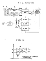
- Fig.l is a block diagram of a conventional white balance control system.
- Light emitted from a light source 1 passes through the optical lens 2 of a colour video camera to be imaged on a camera element 3.
- the camera element 3 produces three electrical signals for the red (R), green (G) and blue (B), which signals are amplified by an R signal amplifier 4, a G signal amplifier 5 and a B signal amplifier 6, respectively.
- R signal amplifier 4 a G signal amplifier 5 and a B signal amplifier 6
- the amplification level of the amplifiers 4, 5 and 6 is controlled by a white balance adjusting circuit 7.
- R and B signals from the photodetector 9 which are converted into photocurrents i R' i B are fed to logarithmic amplifiers 10, 11, respectively, which produce outputs Log i R' log i B .
- the output log (i R/ i B ) changes solely in accordance with a change in the colour temperature of the light source 1, independently of the amount of light which is incident upon the photodetector 9, and hence the white balance adjusting circuit 7 controls the degree of amplification of the R and the B signal amplifiers 4, 6 in a direction to achieve a proper white balance. Specifically, if an object being photographed is defined by white paper, it is required that outputs from the colour video camera maintain a faithful reproduction of the white when amplified by the amplifiers 4 to 6.
- the adjusting circuit 7 operates to change the degree of amplification in the amplifiers 4 and 6 in accordance with the output log (i R /i B ) from the differential amplifier 12, thus achieving a mixing of the signal levels of R and B, which are two of three primary colours R, G and B, in proper proportion, to provide a white balance control.
- a proper white balance can be maintained by detecting the R and B components of light from an object being photographed which is illuminated by sunlight or radiation from a tungsten lamp which can be approximated by the spectrum of radiation from a black body by means of the R/B photodetector 9, in a similar manner as by the television camera element 3.
- the light source comprises a fluorescent lamp or the like
- such source exhibits a peculiar spectrum which is distinct from that of the radiation from a black body, so that when a colour video camera is used which includes circuitry of the type which controls the gain of R and B signals in response to the detection of R and B components of incident light, an offset in the adjustment of the white balance is caused, preventing the maintenance of a good white balance from being achieved.
- a human eye is capable of sensing flickering in the radiation from a fluorescent lamp source, but a light sensitive element can detect such flickering in a more accurate manner.
- the flickering produced by a fluorescent lamp source has a period which is equal to the reciprocal of twice the frequency of a commercial power supply, and the timing or phase of the emission differs between the three primary colours R, G and B.
- natural light or sunbeam has no flickering, and a tungsten lamp exhibits a flickering which is substantially reduced as compared with the flickering of a fluorescent lamp since the thermal time constant of the filament of the tungsten lamp has a higher value. Accordingly, a discrimination between a fluorescent lamp source and other light sources can be made by noting the magnitude of flickering from the source used (such flicker represents a ripple electrically, and hence will be hereafter referred to as a "ripple").
- ripple detecting means which detects a ripple component or components produced by a fluorescent lamp source.
- the detecting means is effective to correct for any offset produced in the white balance control caused by the fluorescent lamp source. In this manner, a proper white balance is maintained with a simple and inexpensive circuit arrangement, without employing a plurality of sensors as in the prior art.
- the ripple detecting means detects whether or not the light source used comprises a fluorescent lamp. It can also be used to determine whether the light source used has a specific colour temperature. Accordingly, when a light source comprises a specific fluorescent lamp source, any offset caused in the white balance control due to this specific lamp source can be corrected, thus assuring a proper white balance.
- a colour temperature conversion filter which is usually disposed in the taking light path can be caused to move out of the light path or a corresponding warning can be produced, thus permitting adverse influences by the colour temperature conversion filter to be removed.
- a block diagram of a white balance control system according to one embodiment of the invention. It is to be understood that similar parts as those shown in Fig.l are designated by like reference characters as before, and their description will not be repeated.
- an output from a differential amplifier 12, which is the same as the differential amplifier 12 shown in Fig.l is applied to a ripple detector circuit 21, in addition to a white balance adjusting circuit 7.
- the ripple detector circuit 21 comprises a bandpass amplifier which selectively amplifies and outputs a ripple component contained in the output log (i R/ i B ) from the differential amplifier 12 which has a period corresponding to twice the frequency f of a commercial power supply.
- the detector circuit 21 also comprises a clamp/peak detector circuit 23 which converts a ripple output from the amplifier 22 into a d.c. voltage having a magnitude which corresponds to the amplitude of the ripple component, and a comparator 24 which compares the level of the d.c. output voltage from the detector circuit 23 to produce a decision output of either "1" or "0".
- the decision output from the comparator 24 is applied to the adjusting circuit 7, which operates to correct for any offset in a white balance whenever the output is equal to "1".
- the colour temperature of an object being photographed increases, the dynamic range of the television camera element 3 is exceeded to upset the balance of colour signals. Accordingly, for colour temperatures above 5,000 to 6,000°K, the colour temperature is converted to a lower value by interposing a colour temperature conversion filter 25, which is commonly referred to as A-type filter, between the optical lens 2 and the camera element 3.
- a colour temperature conversion filter 25 which is commonly referred to as A-type filter
- the conversion filter 25 is effective when it is used with [ sunlight or normal light sources having a high colour temperature.
- the use of such conversion filter 25 is known to present difficulty in achieving a proper white balance. Accordingly, in the present system, the conversion filter 25 is associated with a filter control circuit 26 which is operated in response to an output from the comparator 24.
- the output log (i R/ i B ) from the differential amplifier 12 is applied to the white balance adjusting circuit 7, which in turn controls the degree of amplification of the R signal and the B signal amplifier 4, 6 in order to achieve a proper white balance on the basis of the output which changes with a change in the colour temperature of the light source 1.
- the output trom the amplifier 12 is aiso applied to the bandpass amplifier 22 within the ripple detector circuit 21, and only the ripple component contained in the output log (i R/ i B ) is amplified and output from the amplifer 22.
- Ripple associated with a light source which is contained in light from an object being photographed is illustrated in Fig.3.
- Fig.3 shows a ripple R A for a fluorescent lamp source, and a ripple RB for a tungsten lamp.
- ripple R A or R B is superimposed on a d.c. voltage V A or V B , and the amplified ripple component is applied to the clamp/peak detector circuit 23, which operates to clamp the base of the ripple R A or RB to zero volts and effects a peak detection, whereby a d.c. voltage corresponding to a peak value v PA or v pB is derived.
- This d.c. voltage has a sufficient magnitude to allow a distinction between the ripple RA from the fluorescent lamp source and the ripple RB from other light sources, and hence when the d.c.
- the comparator 24 is capable of producing an output of "1" for a d.c. output voltage corresponding to the ripple R A from the fluorescent lamp source and to produce an output of "0" for a d.c. output voltage corresponding to the ripple R B from other light sources.
- the white balance adjusting circuit 7 When the output signal of "1" from the comparator 24 is applied, the white balance adjusting circuit 7 operates to correct for an offset in the white balance. Specifically, when the R/B photodetector 9 detects light from a fluorescent lamp source which produces a peculiar spectrum, the differential amplifier 12 may produce an output which may cause the adjusting circuit 7 to perform an imperfect operation in seeking to maintain a proper white balance, thus resulting in an offset in the white balance. This in turn causes a picture of an object being photographed to be reproduced in a colour which has more bluish or reddish tone than the actual colour.
- the output from the comparator 24 is applied to the adjusting circuit 7, the latter corrects for an offset in the white balance control, thus bringing the colour tone of the picture of the object being photographed to one which is closer to the actual colour tone.
- a variety of fluorescent lamps are generally of a white or a daylight colour tone and, recently, fluorescent lamps are becoming popular which produce three primary colours of a high colour rendition. While these lamps produce individually specific emissions, they can often be generally regarded as exhibiting a regular offset, by a suitable choice of the spectral response of the photodetector 9.
- an output therefrom may be used to cause the White balance adjusting circuit 7 to change the level of the R and B signals in accordance with the magnitude of the offset, thus maintaining a substantially correct white balance.
- the control circuit 26 which also includes a control mechanism, operates to drive the filter 25 out of the taking light path. This assures a proper white balance adjusting and correcting operation by the adjusting circuit 7.
- radiation from a fluorescent lamp can have a colour temperature which is inherent to the kind of a particular fluorescent . lamp being used. Accordingly, it may be desirable to apply a correction to the white balance control only for a particular fluorescent lamp source or sources, rather than applying a uniform correction for fluorescent lamp sources of every kind.
- An embodiment which is suitable for use in such instance will now be described with reference to Fig.4.
- Fig.4 is a block diagram of a white balance control system according to another embodiment of the invention.
- This embodiment also includes a ripple detector circuit 21 which is constructed in the same manner as shown in Fig.2. An output from a differential amplifier 2 is applied to the ripple detector circuit 21, and a decision output from the comparator 24 of the detector circuit 21 is supplied to one input of a coincidence circuit 29.
- the output Zog (i R/ i B ) from the differential amplifier 12 is passed through a low pass filter (LP F ) 27 which is effective to remove ripple components contained therein.
- a d.c. voltage from the filter 27 is applied to a white balance.adjusting circuit 7 to enable an adjusting operation thereof.
- the output from the filter 27 is also fed to a window comparator 28, which determines if the output from the filter 27 is within a range of voltages which correspond to a particular range of colour temperatures, to provide a decision output of "I" or "0".
- the decision output from the comparator 28 is supplied to the other input of the coincidence circuit 29.
- An output from the coincidence circuit 29 is fed to the adjusting circuit 7 so that the latter is capable of correcting any offset in the white balance control whenever the output from the coincidence circuit 29 is equal to "1".
- a filter control circuit 26 is supplied with an output from the comparator 24 so as to control the colour temperature conversion filter 25 in the same manner as mentioned above.
- the white balance adjusting circuit 7 controls the degree of amplification of the R signal and the B signal amplifier 4, 6 in accordance with such output so as to achieve a proper white balance.
- the output from the differential amplifier 12 is also fed to the ripple detector circuit 21, which operates in the similar manner as mentioned above in connection with Fig.2 to provide a peak value v pA from the clamp/peak detector circuit 23 for the ripple R A associated with a fluorescent lamp source which is sufficiently higher than a peak value vp B (see Fig.3) for the ripple R B associated with other light sources, enabling the comparator 24 to produce an output of "1" for the fluorescent lamp source and an output of "0" otherwise.
- the voltage Log (i R/ i B ) representing the colour temperature which is derived from the differential amplifier 12 is also fed to the window comparator 28.
- the purpose of the window comparator is to detect the colour temperature T 3 (° K ) of a particular fluorescent lamp (as shown in Fig.5) based on the recognition that each fluorescent lamp source has its own inherent colour temperature. In general, the colour temperature of a fluorescent lamp source varies with the response of the fluorescent lamp itself, any contamination of associated accessories such as a reflector, as well as the condition of an object being photographed.
- the purpose of the window comparator 28 is to detect the colour temperature of such particular fluorescent lamp if the voltage log (i R /i B ) is within a range from E 1 to E2 corresponding to a range of temperatures T 1 to T 2 centred about the particular colour temperature T 3 (°K), thereby producing an output of "1" within such range and an output of "0" otherwise.
- the ripple detector circuit 21 produces an output of "1"
- the fluorescent lamp source exhibits a particular colour temperature which is preselected by the window comparator 28, the latter produces an output of "1”.
- the coincidence circuit 29 then produces an output of "I”.
- the output signal of "1" from the coincidence circuit 29 is applied to the adjusting circuit 7, the latter operates to provide a correction for any offset in the white balance control.
- any imperfect white balance controlling operation by the adjusting circuit 7 and hence any offset in the white balance which may be caused by an output from the differential amplifier 12 whenever the R/ B photodetector 9 detects light output from a particular fluorescent lamp source exhibiting a specific colour temperature can be corrected for by changing the level of the R and B signals in accordance with the magnitude of such offset, thus maintaining a substantially proper white balance.
- the window comparator 28 nevertheless produces an output of "0" when this fluorescent lamp is not the particular fluorescent lamp for which the comparator 28 is designed, whereby the coincidence circuit produces an output of "0", preventing a correction of offset in the white balance control.
- fluorescent lamps which are currently in use can be categorized into white type, daylight type and high colour rendition type. While the emissions from these lamps are distinct from each other, fluorescent lamps of the white and the high colour rendition type exhibit colour temperatures in a range from 5,000 to 6,000°K while fluorescent lamps of daylight type exhibit a higher colour temperature in a range from 8,000 to 10,000°K.
- the window comparator 28 by arranging for the window comparator 28 to detect a range of voltages Zog (i R/ i B ), output from the differential amplifier 12, which occur for a range of colour temperatures from 8,000 to 10,000°K (see Fig.5), the coincidence circuit 29 is allowed to produce an output of "1" when a fluorescent lamp of daylight type is used, thereby allowing a correction for any offset in the white balance control by the adjusting circuit 7. In this' manner, a proper white balance control is assured.
- a diffuser panel 8 has been developed which is effective to achieve an additive or integrating action to convert light output from a fluorescent lamp source of white type to light which is closely similar to natural light or light output from a tungsten lamp or the like. In such instance, it may be unnecessary to provide a correction for any offset in the white balance control when a fluorescent lamp source of white type is used.
- the white balance control is performed in response to an output from the differential amplifier 12 which is fed through the low pass filter 27 to the adjusting circuit 7, in the similar manner as effected when a tungsten lamp source is used.
- the invention allows a correction for any offset in the white balance control by the adjusting circuit 7, by arranging for the window comparator 28 to detect a particular fluorescent lamp source or a particular group of fluorescent lamp sources, based on differences in the colour temperature of various fluorescent lamp sources.
- a plurality of window comparators 28 and coincidence circuits 29 may be used so that a plurality of ranges of voltages corresponding to a plurality of ranges of colour temperatures may be detected, thus allowing a simultaneous correction for an offset in the white balance control for a plurality of fluorescent lamp sources.
- the ripple detector circuit 21 detects the ripple R A associated with a fluorescent lamp source and the comparator 24 produces an output of "I"
- this output is fed to the filter control circuit 26 as before, thus driving the colour temperature conversion filter 25 interposed between the optical lens 2 and the camera element 3 out of the taking light path.
- This contributes to achieving an improved white balance control and an offset correction by the adjusting circuit 7.
- a warning may be produced in response to an output from the comparator 24, thus informing a user to remove the conversion filter 25 manually.
Landscapes
- Engineering & Computer Science (AREA)
- Multimedia (AREA)
- Signal Processing (AREA)
- Color Television Image Signal Generators (AREA)
- Processing Of Color Television Signals (AREA)
Abstract
Description
- The invention relates to a white balance control system, and more particularly, to a system which provides an automatic correction for colour temperature in a colour video camera.
- In a colour video camera, an adjustment of white balance is required in order to produce a colour picture of a high quality. If the colour temperature of a light source changes, a corresponding change occurs in the white balance.
- The accompanying Fig.l is a block diagram of a conventional white balance control system. Light emitted from a light source 1 (an object being imaged) passes through the
optical lens 2 of a colour video camera to be imaged on acamera element 3. Thecamera element 3 produces three electrical signals for the red (R), green (G) and blue (B), which signals are amplified by an R signal amplifier 4, aG signal amplifier 5 and aB signal amplifier 6, respectively. In the arrangement shown, the amplification level of theamplifiers B photodetector 9, formed by a light receiving element having a colour filter of a spectral response which is identical to that of thecamera element 3, is located so as to receive light from the light source 1 (an object being photographed), with anopal diffuser plate 8 being disposed in front of thedetector 9. Various colours from an ordinary scene, when added together, infinitely approach the white, and accordingly, the purpose of theopal diffuser plate 8 is to diffuse reflected light from an object being photographed to form an additive sum of light transmitting therethrough over the entire surface of thediffuser plate 8. - R and B signals from the
photodetector 9 which are converted into photocurrents iR' iB are fed tologarithmic amplifiers logarithmic amplifiers differential amplifier 12 which produces an output equal to ℓog i R - ℓog iB = ℓog (iR/iB) which is then fed to.the white balance adjusting circuit 7. The output ℓog (iR/iB) changes solely in accordance with a change in the colour temperature of the light source 1, independently of the amount of light which is incident upon thephotodetector 9, and hence the white balance adjusting circuit 7 controls the degree of amplification of the R and theB signal amplifiers 4, 6 in a direction to achieve a proper white balance. Specifically, if an object being photographed is defined by white paper, it is required that outputs from the colour video camera maintain a faithful reproduction of the white when amplified by the amplifiers 4 to 6. At this end, the adjusting circuit 7 operates to change the degree of amplification in theamplifiers 4 and 6 in accordance with the output ℓog (iR/iB) from thedifferential amplifier 12, thus achieving a mixing of the signal levels of R and B, which are two of three primary colours R, G and B, in proper proportion, to provide a white balance control. - By utilizing the known white balance control system mentioned above, a proper white balance can be maintained by detecting the R and B components of light from an object being photographed which is illuminated by sunlight or radiation from a tungsten lamp which can be approximated by the spectrum of radiation from a black body by means of the R/B
photodetector 9, in a similar manner as by thetelevision camera element 3. However, where the light source comprises a fluorescent lamp or the like, such source exhibits a peculiar spectrum which is distinct from that of the radiation from a black body, so that when a colour video camera is used which includes circuitry of the type which controls the gain of R and B signals in response to the detection of R and B components of incident light, an offset in the adjustment of the white balance is caused, preventing the maintenance of a good white balance from being achieved. - To cope with this problem, there has been proposed a white balance control system (see Japanese Laid-Open Patent Application No.127,376/1982) which includes a sensor capable of detecting the spectra of three primary colours R, G and B and also including another sensor which is capable of detecting a specific spectrum. However, this circuit arrangement requires the provision of a plurality of sensors since there are a variety of fluorescent lamp sources available. If it is desired to cover every kind of lamp source, a large number of sensors must be used, resulting in a complex circuit arrangement and high cost.
- A human eye is capable of sensing flickering in the radiation from a fluorescent lamp source, but a light sensitive element can detect such flickering in a more accurate manner. The flickering produced by a fluorescent lamp source has a period which is equal to the reciprocal of twice the frequency of a commercial power supply, and the timing or phase of the emission differs between the three primary colours R, G and B. On the other hand, natural light or sunbeam has no flickering, and a tungsten lamp exhibits a flickering which is substantially reduced as compared with the flickering of a fluorescent lamp since the thermal time constant of the filament of the tungsten lamp has a higher value. Accordingly, a discrimination between a fluorescent lamp source and other light sources can be made by noting the magnitude of flickering from the source used (such flicker represents a ripple electrically, and hence will be hereafter referred to as a "ripple").
- It is an object of the present invention to provide an improved white balance control system in which the problems associated with known systems are mitigated or removed.
- According to the present invention, there is provided ripple detecting means which detects a ripple component or components produced by a fluorescent lamp source. The detecting means is effective to correct for any offset produced in the white balance control caused by the fluorescent lamp source. In this manner, a proper white balance is maintained with a simple and inexpensive circuit arrangement, without employing a plurality of sensors as in the prior art.
- The ripple detecting means detects whether or not the light source used comprises a fluorescent lamp. It can also be used to determine whether the light source used has a specific colour temperature. Accordingly, when a light source comprises a specific fluorescent lamp source, any offset caused in the white balance control due to this specific lamp source can be corrected, thus assuring a proper white balance.
- In addition, when the light source comprises a fluorescent lamp, a colour temperature conversion filter which is usually disposed in the taking light path can be caused to move out of the light path or a corresponding warning can be produced, thus permitting adverse influences by the colour temperature conversion filter to be removed.
- The invention is described further hereinafter, by way of example only, with reference to the accompanying drawings, wherein:
- Fig.l is a block diagram of an example of a white balance control system of the prior art;
- Fig.2 is a block diagram of a white balance control system according to one embodiment of the invention;
- Fig.3 graphically shows ripples which are treated by a clamp/peak detector circuit shown in Fig.2;
- Fig.4 is a block diagram of a white balance control system according to another embodiment of the invention; and
- Fig.5 graphically shows a change in an output from a differential amplifier of the system of Fig.4 plotted against a change in the colour temperature.
- Referring to Fig.2, there is shown a block diagram of a white balance control system according to one embodiment of the invention. It is to be understood that similar parts as those shown in Fig.l are designated by like reference characters as before, and their description will not be repeated. In the embodiment shown, an output from a
differential amplifier 12, which is the same as thedifferential amplifier 12 shown in Fig.l, is applied to aripple detector circuit 21, in addition to a white balance adjusting circuit 7. Theripple detector circuit 21 comprises a bandpass amplifier which selectively amplifies and outputs a ripple component contained in the output ℓog (iR/iB) from thedifferential amplifier 12 which has a period corresponding to twice the frequency f of a commercial power supply. Thedetector circuit 21 also comprises a clamp/peak detector circuit 23 which converts a ripple output from theamplifier 22 into a d.c. voltage having a magnitude which corresponds to the amplitude of the ripple component, and acomparator 24 which compares the level of the d.c. output voltage from thedetector circuit 23 to produce a decision output of either "1" or "0". The decision output from thecomparator 24 is applied to the adjusting circuit 7, which operates to correct for any offset in a white balance whenever the output is equal to "1". - It is also recognized that when the colour temperature of an object being photographed increases, the dynamic range of the
television camera element 3 is exceeded to upset the balance of colour signals. Accordingly, for colour temperatures above 5,000 to 6,000°K, the colour temperature is converted to a lower value by interposing a colourtemperature conversion filter 25, which is commonly referred to as A-type filter, between theoptical lens 2 and thecamera element 3. It should be noted thatsuch conversion filter 25 is effective when it is used with [ sunlight or normal light sources having a high colour temperature. However, for a light source having a peculiar spectrum such as fluorescent lamp, the use ofsuch conversion filter 25 is known to present difficulty in achieving a proper white balance. Accordingly, in the present system, theconversion filter 25 is associated with afilter control circuit 26 which is operated in response to an output from thecomparator 24. - In operation, the output ℓog (iR/iB) from the
differential amplifier 12 is applied to the white balance adjusting circuit 7, which in turn controls the degree of amplification of the R signal and theB signal amplifier 4, 6 in order to achieve a proper white balance on the basis of the output which changes with a change in the colour temperature of the light source 1. The output trom theamplifier 12 is aiso applied to thebandpass amplifier 22 within theripple detector circuit 21, and only the ripple component contained in the output ℓog (iR/iB) is amplified and output from theamplifer 22. Ripple associated with a light source which is contained in light from an object being photographed is illustrated in Fig.3. By way of example, Fig.3 shows a ripple RA for a fluorescent lamp source, and a ripple RB for a tungsten lamp. It will be apparent from Fig.3 that ripple RA or RB is superimposed on a d.c. voltage VA or VB, and the amplified ripple component is applied to the clamp/peak detector circuit 23, which operates to clamp the base of the ripple RA or RB to zero volts and effects a peak detection, whereby a d.c. voltage corresponding to a peak value vPA or vpB is derived. This d.c. voltage has a sufficient magnitude to allow a distinction between the ripple RA from the fluorescent lamp source and the ripple RB from other light sources, and hence when the d.c. output voltage from thedetector circuit 23 is fed to thecomparator 24, the latter is capable of producing an output of "1" for a d.c. output voltage corresponding to the ripple RA from the fluorescent lamp source and to produce an output of "0" for a d.c. output voltage corresponding to the ripple RB from other light sources. - When the output signal of "1" from the
comparator 24 is applied, the white balance adjusting circuit 7 operates to correct for an offset in the white balance. Specifically, when the R/B photodetector 9 detects light from a fluorescent lamp source which produces a peculiar spectrum, thedifferential amplifier 12 may produce an output which may cause the adjusting circuit 7 to perform an imperfect operation in seeking to maintain a proper white balance, thus resulting in an offset in the white balance. This in turn causes a picture of an object being photographed to be reproduced in a colour which has more bluish or reddish tone than the actual colour. However, when the output from thecomparator 24 is applied to the adjusting circuit 7, the latter corrects for an offset in the white balance control, thus bringing the colour tone of the picture of the object being photographed to one which is closer to the actual colour tone. A variety of fluorescent lamps are generally of a white or a daylight colour tone and, recently, fluorescent lamps are becoming popular which produce three primary colours of a high colour rendition. While these lamps produce individually specific emissions, they can often be generally regarded as exhibiting a regular offset, by a suitable choice of the spectral response of thephotodetector 9. Thus, when the use of a fluorescent lamp is detected by thedetector circuit 21, an output therefrom may be used to cause the White balance adjusting circuit 7 to change the level of the R and B signals in accordance with the magnitude of the offset, thus maintaining a substantially correct white balance. - When the
detector circuit 21 detects the ripple RA from the fluorescent lamp source and thecomparator 24 produces an output of "I", this output is also applied to thefilter control circuit 26 to activate it. Hence, if the colourtemperature conversion filter 25 is interposed between theoptical lens 2 and thecamera element 3 and radiation from a fluorescent lamp source is contained in light from an object being photographed, thecontrol circuit 26, which also includes a control mechanism, operates to drive thefilter 25 out of the taking light path. This assures a proper white balance adjusting and correcting operation by the adjusting circuit 7. - It is to be noted that radiation from a fluorescent lamp can have a colour temperature which is inherent to the kind of a particular fluorescent . lamp being used. Accordingly, it may be desirable to apply a correction to the white balance control only for a particular fluorescent lamp source or sources, rather than applying a uniform correction for fluorescent lamp sources of every kind. An embodiment which is suitable for use in such instance will now be described with reference to Fig.4.
- Fig.4 is a block diagram of a white balance control system according to another embodiment of the invention. In this Figure, parts corresponding to those shown in Figs. 1 and 2 are designated by like reference characters as used in Figs. 1 and 2, and their description will not be repeated. This embodiment also includes a
ripple detector circuit 21 which is constructed in the same manner as shown in Fig.2. An output from adifferential amplifier 2 is applied to theripple detector circuit 21, and a decision output from thecomparator 24 of thedetector circuit 21 is supplied to one input of acoincidence circuit 29. - The output Zog (iR/iB) from the
differential amplifier 12 is passed through a low pass filter (LPF) 27 which is effective to remove ripple components contained therein. A d.c. voltage from thefilter 27 is applied to a white balance.adjusting circuit 7 to enable an adjusting operation thereof. - The output from the
filter 27 is also fed to awindow comparator 28, which determines if the output from thefilter 27 is within a range of voltages which correspond to a particular range of colour temperatures, to provide a decision output of "I" or "0". The decision output from thecomparator 28 is supplied to the other input of thecoincidence circuit 29. An output from thecoincidence circuit 29 is fed to the adjusting circuit 7 so that the latter is capable of correcting any offset in the white balance control whenever the output from thecoincidence circuit 29 is equal to "1". - A
filter control circuit 26 is supplied with an output from thecomparator 24 so as to control the colourtemperature conversion filter 25 in the same manner as mentioned above. - In operation, the output ℓog (iR/iB) from the
differential amplifier 12 is passed through thelow pass filter 27, and its output which is free from ripple components is supplied to the white balance adjusting circuit 7. Accordingly, as the output ℓog (iR/iB) changes with a change in the colour temperature of the light source 1 (see Fig.5), the white balance adjusting circuit 7 controls the degree of amplification of the R signal and theB signal amplifier 4, 6 in accordance with such output so as to achieve a proper white balance. The output from thedifferential amplifier 12 is also fed to theripple detector circuit 21, which operates in the similar manner as mentioned above in connection with Fig.2 to provide a peak value vpA from the clamp/peak detector circuit 23 for the ripple RA associated with a fluorescent lamp source which is sufficiently higher than a peak value vpB (see Fig.3) for the ripple RB associated with other light sources, enabling thecomparator 24 to produce an output of "1" for the fluorescent lamp source and an output of "0" otherwise. - After being passed through the
low pass filter 27, the voltage Log (iR/iB) representing the colour temperature which is derived from thedifferential amplifier 12 is also fed to thewindow comparator 28. The purpose of the window comparator is to detect the colour temperature T3 (°K) of a particular fluorescent lamp (as shown in Fig.5) based on the recognition that each fluorescent lamp source has its own inherent colour temperature. In general, the colour temperature of a fluorescent lamp source varies with the response of the fluorescent lamp itself, any contamination of associated accessories such as a reflector, as well as the condition of an object being photographed. Accordingly, the purpose of thewindow comparator 28 is to detect the colour temperature of such particular fluorescent lamp if the voltage ℓog (iR/iB) is within a range from E1 to E2 corresponding to a range of temperatures T1 to T2 centred about the particular colour temperature T3 (°K), thereby producing an output of "1" within such range and an output of "0" otherwise. - It will be seen therefore that when a fluorescent lamp is used as a light source for the colour video camera, the
ripple detector circuit 21 produces an output of "1", and if the fluorescent lamp source exhibits a particular colour temperature which is preselected by thewindow comparator 28, the latter produces an output of "1". Thecoincidence circuit 29 then produces an output of "I". When the output signal of "1" from thecoincidence circuit 29 is applied to the adjusting circuit 7, the latter operates to provide a correction for any offset in the white balance control. Thus any imperfect white balance controlling operation by the adjusting circuit 7 and hence any offset in the white balance which may be caused by an output from thedifferential amplifier 12 whenever the R/B photodetector 9 detects light output from a particular fluorescent lamp source exhibiting a specific colour temperature can be corrected for by changing the level of the R and B signals in accordance with the magnitude of such offset, thus maintaining a substantially proper white balance. - If the light source used comprises a fluorescent lamp and the
ripple detector circuit 21 produces an output of "1", thewindow comparator 28 nevertheless produces an output of "0" when this fluorescent lamp is not the particular fluorescent lamp for which thecomparator 28 is designed, whereby the coincidence circuit produces an output of "0", preventing a correction of offset in the white balance control. - Considering varieties of fluorescent lamps, fluorescent lamps which are currently in use can be categorized into white type, daylight type and high colour rendition type. While the emissions from these lamps are distinct from each other, fluorescent lamps of the white and the high colour rendition type exhibit colour temperatures in a range from 5,000 to 6,000°K while fluorescent lamps of daylight type exhibit a higher colour temperature in a range from 8,000 to 10,000°K. Accordingly, by arranging for the
window comparator 28 to detect a range of voltages Zog (iR/iB), output from thedifferential amplifier 12, which occur for a range of colour temperatures from 8,000 to 10,000°K (see Fig.5), thecoincidence circuit 29 is allowed to produce an output of "1" when a fluorescent lamp of daylight type is used, thereby allowing a correction for any offset in the white balance control by the adjusting circuit 7. In this' manner, a proper white balance control is assured. - Recently, a
diffuser panel 8 has been developed which is effective to achieve an additive or integrating action to convert light output from a fluorescent lamp source of white type to light which is closely similar to natural light or light output from a tungsten lamp or the like. In such instance, it may be unnecessary to provide a correction for any offset in the white balance control when a fluorescent lamp source of white type is used. Thus when using fluorescent lamp sources other than a particular fluorescent lamp of daylight type, the white balance control is performed in response to an output from thedifferential amplifier 12 which is fed through thelow pass filter 27 to the adjusting circuit 7, in the similar manner as effected when a tungsten lamp source is used. - It is expected that the kinds of fluorescent lamps available will increase still further in future, and the invention allows a correction for any offset in the white balance control by the adjusting circuit 7, by arranging for the
window comparator 28 to detect a particular fluorescent lamp source or a particular group of fluorescent lamp sources, based on differences in the colour temperature of various fluorescent lamp sources. Alternatively, a plurality ofwindow comparators 28 andcoincidence circuits 29 may be used so that a plurality of ranges of voltages corresponding to a plurality of ranges of colour temperatures may be detected, thus allowing a simultaneous correction for an offset in the white balance control for a plurality of fluorescent lamp sources. - When the
ripple detector circuit 21 detects the ripple RA associated with a fluorescent lamp source and thecomparator 24 produces an output of "I", this output is fed to thefilter control circuit 26 as before, thus driving the colourtemperature conversion filter 25 interposed between theoptical lens 2 and thecamera element 3 out of the taking light path. This contributes to achieving an improved white balance control and an offset correction by the adjusting circuit 7. As a further alternative, instead of automatically moving theconversion filter 25 out of the taking light path, a warning may be produced in response to an output from thecomparator 24, thus informing a user to remove theconversion filter 25 manually. - In the embodiments described above, two colours R and B of the three primary colours have been detected to control the level of the R and B signals in order to achieve a white balance, but all the three primary colours may be detected to control the level of the three colour signals R, G and B without departing from the invention.
Claims (12)
Applications Claiming Priority (4)
| Application Number | Priority Date | Filing Date | Title |
|---|---|---|---|
| JP58015687A JPS59141888A (en) | 1983-02-02 | 1983-02-02 | Automatic white balancing circuit |
| JP15687/83 | 1983-02-02 | ||
| JP192234/83 | 1983-10-14 | ||
| JP58192234A JPS6083489A (en) | 1983-10-14 | 1983-10-14 | Automatic white balancing circuit |
Publications (2)
| Publication Number | Publication Date |
|---|---|
| EP0116435A1 true EP0116435A1 (en) | 1984-08-22 |
| EP0116435B1 EP0116435B1 (en) | 1987-05-06 |
Family
ID=26351876
Family Applications (1)
| Application Number | Title | Priority Date | Filing Date |
|---|---|---|---|
| EP84300617A Expired EP0116435B1 (en) | 1983-02-02 | 1984-02-01 | White balance control system |
Country Status (3)
| Country | Link |
|---|---|
| US (1) | US4595946A (en) |
| EP (1) | EP0116435B1 (en) |
| DE (1) | DE3463600D1 (en) |
Cited By (2)
| Publication number | Priority date | Publication date | Assignee | Title |
|---|---|---|---|---|
| EP0224904A3 (en) * | 1985-12-04 | 1989-03-15 | Hitachi, Ltd. | White balance adjusting device of color video camera |
| EP1944967A2 (en) | 2006-12-15 | 2008-07-16 | STMicroelectronics Asia Pacific Pte Ltd. | System and method for flicker DC offset detection and correction |
Families Citing this family (26)
| Publication number | Priority date | Publication date | Assignee | Title |
|---|---|---|---|---|
| US4833525A (en) * | 1985-03-29 | 1989-05-23 | Canon Kabushiki Kaisha | High speed color balance adjusting device capable of compensating for a flickering light source |
| US4879591A (en) * | 1986-01-31 | 1989-11-07 | Canon Kabushiki Kaisha | Image pickup apparatus compensating an image signal for variations in color temperature |
| US5170069A (en) * | 1986-05-21 | 1992-12-08 | Canon Kabushiki Kaisha | Image pickup apparatus |
| DE3750012T2 (en) * | 1986-09-09 | 1994-09-29 | Fuji Photo Film Co Ltd | Electronic still camera to compensate for the color temperature dependence of color video signals. |
| JPS63105580A (en) * | 1986-10-22 | 1988-05-10 | Hitachi Ltd | Television camera |
| US5021875A (en) * | 1987-02-18 | 1991-06-04 | Minolta Camera Kabushiki Kaisha | Automatic white-balance adjusting apparatus with reduced sensitivity to transient light conditions |
| US4918519A (en) * | 1987-04-23 | 1990-04-17 | Canon Kabushiki Kaisha | Color image sensing apparatus having color balance adjustment |
| US4899212A (en) * | 1987-08-28 | 1990-02-06 | Fuji Photo Film Co., Ltd. | White balance adjusting device for a camera |
| JP2508951Y2 (en) * | 1988-02-03 | 1996-08-28 | 富士写真フイルム株式会社 | White balance adjuster |
| US5283635A (en) * | 1988-06-03 | 1994-02-01 | Canon Kabushiki Kaisha | White balance adjusting device with plural thresholds for range control |
| JP2890414B2 (en) * | 1988-08-08 | 1999-05-17 | キヤノン株式会社 | Imaging device |
| US5087936A (en) * | 1988-09-08 | 1992-02-11 | Fuji Photo Film Co., Ltd. | Camera |
| JPH02189091A (en) * | 1989-01-18 | 1990-07-25 | Mitsubishi Electric Corp | Automatic white balance circuit |
| US5008739A (en) * | 1989-02-13 | 1991-04-16 | Eastman Kodak Company | Real-time digital processor for producing full resolution color signals from a multi-color image sensor |
| JPH031791A (en) * | 1989-05-30 | 1991-01-08 | Sony Corp | Automatic white balance circuit |
| US5014014A (en) * | 1989-06-06 | 1991-05-07 | Science Applications International Corporation | Plane wave transformer linac structure |
| US5223921A (en) * | 1990-04-27 | 1993-06-29 | Sanyo Electric Co., Ltd. | White balance adjusting apparatus for automatically adjusting white balance on the basis of a color information signal obtained from an image-sensing device |
| US5313277A (en) * | 1990-10-30 | 1994-05-17 | Canon Kabushiki Kaisha | Image pickup device having white balance control function |
| JPH06165189A (en) * | 1992-11-25 | 1994-06-10 | Nikon Corp | White balance adjustment device |
| JPH06189332A (en) * | 1992-12-21 | 1994-07-08 | Hitachi Ltd | White balance correction device |
| US5598000A (en) * | 1996-02-22 | 1997-01-28 | Popat; Pradeep P. | Dual-mode automatic window covering system responsive to AC-induced flicker in ambient illumination |
| US6271884B1 (en) * | 1999-09-28 | 2001-08-07 | Conexant Systems, Inc. | Image flicker reduction with fluorescent lighting |
| US6781626B1 (en) | 2000-01-13 | 2004-08-24 | Biomorphic Vlsi, Inc. | System and method of color interpolation |
| US6757012B1 (en) | 2000-01-13 | 2004-06-29 | Biomorphic Vlsi, Inc. | Color selection for sparse color image reconstruction |
| US6876384B1 (en) | 2000-04-19 | 2005-04-05 | Biomorphic Vlsi, Inc. | Pixel selective white balancing |
| EP2262228A1 (en) | 2009-06-09 | 2010-12-15 | Global IP Solutions (GIPS) AB | Detection and supression of flicker in a sequence of images |
Citations (2)
| Publication number | Priority date | Publication date | Assignee | Title |
|---|---|---|---|---|
| US4281337A (en) * | 1978-03-15 | 1981-07-28 | Sony Corporation | Apparatus for detecting the color temperature of a source of light and automatic white balancing means for use therewith |
| DE3236269A1 (en) * | 1981-10-01 | 1983-04-21 | Nippon Kogaku K.K., Tokyo | WHITE LEVEL ADJUSTMENT DEVICE FOR COLOR TV CAMERAS |
Family Cites Families (4)
| Publication number | Priority date | Publication date | Assignee | Title |
|---|---|---|---|---|
| USRE28774E (en) * | 1970-01-17 | 1976-04-13 | Sony Corporation | White balance control system |
| JPS57127376A (en) * | 1981-01-30 | 1982-08-07 | Nippon Kogaku Kk <Nikon> | White balance circuit |
| JPH0642740B2 (en) * | 1981-05-12 | 1994-06-01 | 富士写真フイルム株式会社 | Image recording / reproducing device |
| JPS58147721A (en) * | 1982-02-26 | 1983-09-02 | Canon Inc | Camera |
-
1984
- 1984-01-31 US US06/575,344 patent/US4595946A/en not_active Expired - Lifetime
- 1984-02-01 EP EP84300617A patent/EP0116435B1/en not_active Expired
- 1984-02-01 DE DE8484300617T patent/DE3463600D1/en not_active Expired
Patent Citations (2)
| Publication number | Priority date | Publication date | Assignee | Title |
|---|---|---|---|---|
| US4281337A (en) * | 1978-03-15 | 1981-07-28 | Sony Corporation | Apparatus for detecting the color temperature of a source of light and automatic white balancing means for use therewith |
| DE3236269A1 (en) * | 1981-10-01 | 1983-04-21 | Nippon Kogaku K.K., Tokyo | WHITE LEVEL ADJUSTMENT DEVICE FOR COLOR TV CAMERAS |
Cited By (3)
| Publication number | Priority date | Publication date | Assignee | Title |
|---|---|---|---|---|
| EP0224904A3 (en) * | 1985-12-04 | 1989-03-15 | Hitachi, Ltd. | White balance adjusting device of color video camera |
| EP1944967A2 (en) | 2006-12-15 | 2008-07-16 | STMicroelectronics Asia Pacific Pte Ltd. | System and method for flicker DC offset detection and correction |
| EP1944967A3 (en) * | 2006-12-15 | 2010-11-17 | STMicroelectronics Asia Pacific Pte Ltd. | System and method for flicker DC offset detection and correction |
Also Published As
| Publication number | Publication date |
|---|---|
| DE3463600D1 (en) | 1987-06-11 |
| US4595946A (en) | 1986-06-17 |
| EP0116435B1 (en) | 1987-05-06 |
Similar Documents
| Publication | Publication Date | Title |
|---|---|---|
| US4595946A (en) | White balance control system including a fluorescent light ripple detector | |
| US5293238A (en) | Televison camera | |
| US4847680A (en) | Image pickup apparatus with white balance control | |
| US4682210A (en) | Automatic white balance adjusting circuit for image pickup device | |
| JPH01503828A (en) | Still image video camera with common circuitry for color balance and exposure control | |
| JPH0758226B2 (en) | Light source detection device | |
| US4833525A (en) | High speed color balance adjusting device capable of compensating for a flickering light source | |
| JPS59141888A (en) | Automatic white balancing circuit | |
| US4687919A (en) | A lighting control device in manuscript reproduction equipment | |
| US5255077A (en) | White balance control based upon magnitude of flicker | |
| US5087936A (en) | Camera | |
| US5239368A (en) | High speed color balance adjusting device capable of compensating for a flickering light source | |
| US4590512A (en) | Circuit for detecting the ratio of intensities of the color components of light | |
| JPS62189891A (en) | Automatic white balance device | |
| US5315394A (en) | Auto-iris method and apparatus for imaging device | |
| JPH056399B2 (en) | ||
| JP2811652B2 (en) | Video camera | |
| JPS60240291A (en) | White balance device | |
| EP0420621B1 (en) | Method and apparatus for effecting white balance control in an image pickup apparatus | |
| JPS62133884A (en) | Automatic white balance adjusting device | |
| JP2502502B2 (en) | Camera device | |
| JP2890414B2 (en) | Imaging device | |
| JPS62159595A (en) | Automatic white balance device | |
| JPS63141488A (en) | Imaging device | |
| JPS63236931A (en) | White balance detector |
Legal Events
| Date | Code | Title | Description |
|---|---|---|---|
| PUAI | Public reference made under article 153(3) epc to a published international application that has entered the european phase |
Free format text: ORIGINAL CODE: 0009012 |
|
| AK | Designated contracting states |
Designated state(s): DE FR GB IT NL |
|
| 17P | Request for examination filed |
Effective date: 19840713 |
|
| ITF | It: translation for a ep patent filed | ||
| GRAA | (expected) grant |
Free format text: ORIGINAL CODE: 0009210 |
|
| AK | Designated contracting states |
Kind code of ref document: B1 Designated state(s): DE FR GB IT NL |
|
| REF | Corresponds to: |
Ref document number: 3463600 Country of ref document: DE Date of ref document: 19870611 |
|
| ET | Fr: translation filed | ||
| PLBE | No opposition filed within time limit |
Free format text: ORIGINAL CODE: 0009261 |
|
| STAA | Information on the status of an ep patent application or granted ep patent |
Free format text: STATUS: NO OPPOSITION FILED WITHIN TIME LIMIT |
|
| 26N | No opposition filed | ||
| PG25 | Lapsed in a contracting state [announced via postgrant information from national office to epo] |
Ref country code: NL Effective date: 19880901 |
|
| NLV4 | Nl: lapsed or anulled due to non-payment of the annual fee | ||
| ITTA | It: last paid annual fee | ||
| REG | Reference to a national code |
Ref country code: GB Ref legal event code: IF02 |
|
| PGFP | Annual fee paid to national office [announced via postgrant information from national office to epo] |
Ref country code: GB Payment date: 20020130 Year of fee payment: 19 |
|
| PGFP | Annual fee paid to national office [announced via postgrant information from national office to epo] |
Ref country code: FR Payment date: 20020212 Year of fee payment: 19 |
|
| PGFP | Annual fee paid to national office [announced via postgrant information from national office to epo] |
Ref country code: DE Payment date: 20020227 Year of fee payment: 19 |
|
| PG25 | Lapsed in a contracting state [announced via postgrant information from national office to epo] |
Ref country code: GB Free format text: LAPSE BECAUSE OF NON-PAYMENT OF DUE FEES Effective date: 20030201 |
|
| PG25 | Lapsed in a contracting state [announced via postgrant information from national office to epo] |
Ref country code: DE Free format text: LAPSE BECAUSE OF NON-PAYMENT OF DUE FEES Effective date: 20030902 |
|
| GBPC | Gb: european patent ceased through non-payment of renewal fee | ||
| PG25 | Lapsed in a contracting state [announced via postgrant information from national office to epo] |
Ref country code: FR Free format text: LAPSE BECAUSE OF NON-PAYMENT OF DUE FEES Effective date: 20031031 |
|
| REG | Reference to a national code |
Ref country code: FR Ref legal event code: ST |