EP0113434A1 - Dispositif photovoltaique - Google Patents
Dispositif photovoltaique Download PDFInfo
- Publication number
- EP0113434A1 EP0113434A1 EP83112159A EP83112159A EP0113434A1 EP 0113434 A1 EP0113434 A1 EP 0113434A1 EP 83112159 A EP83112159 A EP 83112159A EP 83112159 A EP83112159 A EP 83112159A EP 0113434 A1 EP0113434 A1 EP 0113434A1
- Authority
- EP
- European Patent Office
- Prior art keywords
- region
- amorphous
- crystalline
- regions
- solar cell
- Prior art date
- Legal status (The legal status is an assumption and is not a legal conclusion. Google has not performed a legal analysis and makes no representation as to the accuracy of the status listed.)
- Granted
Links
- 239000004065 semiconductor Substances 0.000 claims abstract description 93
- 238000000034 method Methods 0.000 claims abstract description 44
- 239000000758 substrate Substances 0.000 claims description 20
- 239000010409 thin film Substances 0.000 claims description 16
- 230000001788 irregular Effects 0.000 claims description 8
- 230000003247 decreasing effect Effects 0.000 claims description 6
- 229910010272 inorganic material Inorganic materials 0.000 claims description 4
- 239000011147 inorganic material Substances 0.000 claims description 4
- 239000011368 organic material Substances 0.000 claims 3
- 238000004519 manufacturing process Methods 0.000 abstract description 16
- 206010034972 Photosensitivity reaction Diseases 0.000 abstract description 2
- 230000036211 photosensitivity Effects 0.000 abstract description 2
- 229910021417 amorphous silicon Inorganic materials 0.000 description 34
- 238000006243 chemical reaction Methods 0.000 description 19
- 239000000463 material Substances 0.000 description 17
- 239000010408 film Substances 0.000 description 13
- 229910021420 polycrystalline silicon Inorganic materials 0.000 description 13
- CIWBSHSKHKDKBQ-JLAZNSOCSA-N Ascorbic acid Chemical compound OC[C@H](O)[C@H]1OC(=O)C(O)=C1O CIWBSHSKHKDKBQ-JLAZNSOCSA-N 0.000 description 11
- 229910021424 microcrystalline silicon Inorganic materials 0.000 description 8
- 229910001218 Gallium arsenide Inorganic materials 0.000 description 7
- 238000010586 diagram Methods 0.000 description 7
- 229910021421 monocrystalline silicon Inorganic materials 0.000 description 7
- HBMJWWWQQXIZIP-UHFFFAOYSA-N silicon carbide Chemical compound [Si+]#[C-] HBMJWWWQQXIZIP-UHFFFAOYSA-N 0.000 description 6
- 239000012535 impurity Substances 0.000 description 5
- 238000010521 absorption reaction Methods 0.000 description 4
- 238000005229 chemical vapour deposition Methods 0.000 description 4
- 238000000151 deposition Methods 0.000 description 4
- AMGQUBHHOARCQH-UHFFFAOYSA-N indium;oxotin Chemical compound [In].[Sn]=O AMGQUBHHOARCQH-UHFFFAOYSA-N 0.000 description 4
- 229910000577 Silicon-germanium Inorganic materials 0.000 description 3
- 229910052782 aluminium Inorganic materials 0.000 description 3
- XAGFODPZIPBFFR-UHFFFAOYSA-N aluminium Chemical compound [Al] XAGFODPZIPBFFR-UHFFFAOYSA-N 0.000 description 3
- 239000002178 crystalline material Substances 0.000 description 3
- 238000005215 recombination Methods 0.000 description 3
- 230000006798 recombination Effects 0.000 description 3
- 239000007787 solid Substances 0.000 description 3
- 238000004544 sputter deposition Methods 0.000 description 3
- 230000007704 transition Effects 0.000 description 3
- 239000004642 Polyimide Substances 0.000 description 2
- 229910020328 SiSn Inorganic materials 0.000 description 2
- 239000000919 ceramic Substances 0.000 description 2
- 229910021419 crystalline silicon Inorganic materials 0.000 description 2
- 238000000354 decomposition reaction Methods 0.000 description 2
- 230000008021 deposition Effects 0.000 description 2
- 230000006866 deterioration Effects 0.000 description 2
- 238000009792 diffusion process Methods 0.000 description 2
- SCCCLDWUZODEKG-UHFFFAOYSA-N germanide Chemical compound [GeH3-] SCCCLDWUZODEKG-UHFFFAOYSA-N 0.000 description 2
- 229910052732 germanium Inorganic materials 0.000 description 2
- 239000011521 glass Substances 0.000 description 2
- 238000005468 ion implantation Methods 0.000 description 2
- 238000007733 ion plating Methods 0.000 description 2
- 150000002500 ions Chemical class 0.000 description 2
- 229910052751 metal Inorganic materials 0.000 description 2
- 239000002184 metal Substances 0.000 description 2
- 229920001721 polyimide Polymers 0.000 description 2
- 229910052710 silicon Inorganic materials 0.000 description 2
- 229910010271 silicon carbide Inorganic materials 0.000 description 2
- 238000001228 spectrum Methods 0.000 description 2
- 229910001220 stainless steel Inorganic materials 0.000 description 2
- 239000010935 stainless steel Substances 0.000 description 2
- 238000006467 substitution reaction Methods 0.000 description 2
- JBRZTFJDHDCESZ-UHFFFAOYSA-N AsGa Chemical compound [As]#[Ga] JBRZTFJDHDCESZ-UHFFFAOYSA-N 0.000 description 1
- 229910004613 CdTe Inorganic materials 0.000 description 1
- 206010034960 Photophobia Diseases 0.000 description 1
- 229910004541 SiN Inorganic materials 0.000 description 1
- XUIMIQQOPSSXEZ-UHFFFAOYSA-N Silicon Chemical compound [Si] XUIMIQQOPSSXEZ-UHFFFAOYSA-N 0.000 description 1
- 238000000137 annealing Methods 0.000 description 1
- 125000004429 atom Chemical group 0.000 description 1
- 230000015572 biosynthetic process Effects 0.000 description 1
- 229910052980 cadmium sulfide Inorganic materials 0.000 description 1
- 239000000969 carrier Substances 0.000 description 1
- 239000000470 constituent Substances 0.000 description 1
- 239000013078 crystal Substances 0.000 description 1
- 230000000694 effects Effects 0.000 description 1
- 230000005684 electric field Effects 0.000 description 1
- 238000000313 electron-beam-induced deposition Methods 0.000 description 1
- 230000002708 enhancing effect Effects 0.000 description 1
- 239000007789 gas Substances 0.000 description 1
- GNPVGFCGXDBREM-UHFFFAOYSA-N germanium atom Chemical compound [Ge] GNPVGFCGXDBREM-UHFFFAOYSA-N 0.000 description 1
- APFVFJFRJDLVQX-UHFFFAOYSA-N indium atom Chemical group [In] APFVFJFRJDLVQX-UHFFFAOYSA-N 0.000 description 1
- 229910003480 inorganic solid Inorganic materials 0.000 description 1
- 230000031700 light absorption Effects 0.000 description 1
- 208000013469 light sensitivity Diseases 0.000 description 1
- 230000013011 mating Effects 0.000 description 1
- 239000011159 matrix material Substances 0.000 description 1
- 239000007769 metal material Substances 0.000 description 1
- 239000013080 microcrystalline material Substances 0.000 description 1
- 229910003465 moissanite Inorganic materials 0.000 description 1
- 238000001451 molecular beam epitaxy Methods 0.000 description 1
- 230000003287 optical effect Effects 0.000 description 1
- 125000004430 oxygen atom Chemical group O* 0.000 description 1
- 239000010703 silicon Substances 0.000 description 1
- HQVNEWCFYHHQES-UHFFFAOYSA-N silicon nitride Chemical compound N12[Si]34N5[Si]62N3[Si]51N64 HQVNEWCFYHHQES-UHFFFAOYSA-N 0.000 description 1
- 229910001134 stannide Inorganic materials 0.000 description 1
- 238000001771 vacuum deposition Methods 0.000 description 1
- 238000005019 vapor deposition process Methods 0.000 description 1
Images


Classifications
-
- H—ELECTRICITY
- H01—ELECTRIC ELEMENTS
- H01L—SEMICONDUCTOR DEVICES NOT COVERED BY CLASS H10
- H01L31/00—Semiconductor devices sensitive to infrared radiation, light, electromagnetic radiation of shorter wavelength or corpuscular radiation and specially adapted either for the conversion of the energy of such radiation into electrical energy or for the control of electrical energy by such radiation; Processes or apparatus specially adapted for the manufacture or treatment thereof or of parts thereof; Details thereof
- H01L31/04—Semiconductor devices sensitive to infrared radiation, light, electromagnetic radiation of shorter wavelength or corpuscular radiation and specially adapted either for the conversion of the energy of such radiation into electrical energy or for the control of electrical energy by such radiation; Processes or apparatus specially adapted for the manufacture or treatment thereof or of parts thereof; Details thereof adapted as photovoltaic [PV] conversion devices
- H01L31/06—Semiconductor devices sensitive to infrared radiation, light, electromagnetic radiation of shorter wavelength or corpuscular radiation and specially adapted either for the conversion of the energy of such radiation into electrical energy or for the control of electrical energy by such radiation; Processes or apparatus specially adapted for the manufacture or treatment thereof or of parts thereof; Details thereof adapted as photovoltaic [PV] conversion devices characterised by at least one potential-jump barrier or surface barrier
- H01L31/072—Semiconductor devices sensitive to infrared radiation, light, electromagnetic radiation of shorter wavelength or corpuscular radiation and specially adapted either for the conversion of the energy of such radiation into electrical energy or for the control of electrical energy by such radiation; Processes or apparatus specially adapted for the manufacture or treatment thereof or of parts thereof; Details thereof adapted as photovoltaic [PV] conversion devices characterised by at least one potential-jump barrier or surface barrier the potential barriers being only of the PN heterojunction type
- H01L31/0745—Semiconductor devices sensitive to infrared radiation, light, electromagnetic radiation of shorter wavelength or corpuscular radiation and specially adapted either for the conversion of the energy of such radiation into electrical energy or for the control of electrical energy by such radiation; Processes or apparatus specially adapted for the manufacture or treatment thereof or of parts thereof; Details thereof adapted as photovoltaic [PV] conversion devices characterised by at least one potential-jump barrier or surface barrier the potential barriers being only of the PN heterojunction type comprising a AIVBIV heterojunction, e.g. Si/Ge, SiGe/Si or Si/SiC solar cells
- H01L31/0747—Semiconductor devices sensitive to infrared radiation, light, electromagnetic radiation of shorter wavelength or corpuscular radiation and specially adapted either for the conversion of the energy of such radiation into electrical energy or for the control of electrical energy by such radiation; Processes or apparatus specially adapted for the manufacture or treatment thereof or of parts thereof; Details thereof adapted as photovoltaic [PV] conversion devices characterised by at least one potential-jump barrier or surface barrier the potential barriers being only of the PN heterojunction type comprising a AIVBIV heterojunction, e.g. Si/Ge, SiGe/Si or Si/SiC solar cells comprising a heterojunction of crystalline and amorphous materials, e.g. heterojunction with intrinsic thin layer or HIT® solar cells; solar cells
-
- H—ELECTRICITY
- H01—ELECTRIC ELEMENTS
- H01L—SEMICONDUCTOR DEVICES NOT COVERED BY CLASS H10
- H01L31/00—Semiconductor devices sensitive to infrared radiation, light, electromagnetic radiation of shorter wavelength or corpuscular radiation and specially adapted either for the conversion of the energy of such radiation into electrical energy or for the control of electrical energy by such radiation; Processes or apparatus specially adapted for the manufacture or treatment thereof or of parts thereof; Details thereof
- H01L31/02—Details
- H01L31/0236—Special surface textures
- H01L31/02363—Special surface textures of the semiconductor body itself, e.g. textured active layers
-
- H—ELECTRICITY
- H01—ELECTRIC ELEMENTS
- H01L—SEMICONDUCTOR DEVICES NOT COVERED BY CLASS H10
- H01L31/00—Semiconductor devices sensitive to infrared radiation, light, electromagnetic radiation of shorter wavelength or corpuscular radiation and specially adapted either for the conversion of the energy of such radiation into electrical energy or for the control of electrical energy by such radiation; Processes or apparatus specially adapted for the manufacture or treatment thereof or of parts thereof; Details thereof
- H01L31/0248—Semiconductor devices sensitive to infrared radiation, light, electromagnetic radiation of shorter wavelength or corpuscular radiation and specially adapted either for the conversion of the energy of such radiation into electrical energy or for the control of electrical energy by such radiation; Processes or apparatus specially adapted for the manufacture or treatment thereof or of parts thereof; Details thereof characterised by their semiconductor bodies
- H01L31/036—Semiconductor devices sensitive to infrared radiation, light, electromagnetic radiation of shorter wavelength or corpuscular radiation and specially adapted either for the conversion of the energy of such radiation into electrical energy or for the control of electrical energy by such radiation; Processes or apparatus specially adapted for the manufacture or treatment thereof or of parts thereof; Details thereof characterised by their semiconductor bodies characterised by their crystalline structure or particular orientation of the crystalline planes
- H01L31/0368—Semiconductor devices sensitive to infrared radiation, light, electromagnetic radiation of shorter wavelength or corpuscular radiation and specially adapted either for the conversion of the energy of such radiation into electrical energy or for the control of electrical energy by such radiation; Processes or apparatus specially adapted for the manufacture or treatment thereof or of parts thereof; Details thereof characterised by their semiconductor bodies characterised by their crystalline structure or particular orientation of the crystalline planes including polycrystalline semiconductors
- H01L31/03682—Semiconductor devices sensitive to infrared radiation, light, electromagnetic radiation of shorter wavelength or corpuscular radiation and specially adapted either for the conversion of the energy of such radiation into electrical energy or for the control of electrical energy by such radiation; Processes or apparatus specially adapted for the manufacture or treatment thereof or of parts thereof; Details thereof characterised by their semiconductor bodies characterised by their crystalline structure or particular orientation of the crystalline planes including polycrystalline semiconductors including only elements of Group IV of the Periodic System
- H01L31/03685—Semiconductor devices sensitive to infrared radiation, light, electromagnetic radiation of shorter wavelength or corpuscular radiation and specially adapted either for the conversion of the energy of such radiation into electrical energy or for the control of electrical energy by such radiation; Processes or apparatus specially adapted for the manufacture or treatment thereof or of parts thereof; Details thereof characterised by their semiconductor bodies characterised by their crystalline structure or particular orientation of the crystalline planes including polycrystalline semiconductors including only elements of Group IV of the Periodic System including microcrystalline silicon, uc-Si
-
- H—ELECTRICITY
- H01—ELECTRIC ELEMENTS
- H01L—SEMICONDUCTOR DEVICES NOT COVERED BY CLASS H10
- H01L31/00—Semiconductor devices sensitive to infrared radiation, light, electromagnetic radiation of shorter wavelength or corpuscular radiation and specially adapted either for the conversion of the energy of such radiation into electrical energy or for the control of electrical energy by such radiation; Processes or apparatus specially adapted for the manufacture or treatment thereof or of parts thereof; Details thereof
- H01L31/04—Semiconductor devices sensitive to infrared radiation, light, electromagnetic radiation of shorter wavelength or corpuscular radiation and specially adapted either for the conversion of the energy of such radiation into electrical energy or for the control of electrical energy by such radiation; Processes or apparatus specially adapted for the manufacture or treatment thereof or of parts thereof; Details thereof adapted as photovoltaic [PV] conversion devices
- H01L31/06—Semiconductor devices sensitive to infrared radiation, light, electromagnetic radiation of shorter wavelength or corpuscular radiation and specially adapted either for the conversion of the energy of such radiation into electrical energy or for the control of electrical energy by such radiation; Processes or apparatus specially adapted for the manufacture or treatment thereof or of parts thereof; Details thereof adapted as photovoltaic [PV] conversion devices characterised by at least one potential-jump barrier or surface barrier
- H01L31/078—Semiconductor devices sensitive to infrared radiation, light, electromagnetic radiation of shorter wavelength or corpuscular radiation and specially adapted either for the conversion of the energy of such radiation into electrical energy or for the control of electrical energy by such radiation; Processes or apparatus specially adapted for the manufacture or treatment thereof or of parts thereof; Details thereof adapted as photovoltaic [PV] conversion devices characterised by at least one potential-jump barrier or surface barrier including different types of potential barriers provided for in two or more of groups H01L31/062 - H01L31/075
-
- Y—GENERAL TAGGING OF NEW TECHNOLOGICAL DEVELOPMENTS; GENERAL TAGGING OF CROSS-SECTIONAL TECHNOLOGIES SPANNING OVER SEVERAL SECTIONS OF THE IPC; TECHNICAL SUBJECTS COVERED BY FORMER USPC CROSS-REFERENCE ART COLLECTIONS [XRACs] AND DIGESTS
- Y02—TECHNOLOGIES OR APPLICATIONS FOR MITIGATION OR ADAPTATION AGAINST CLIMATE CHANGE
- Y02E—REDUCTION OF GREENHOUSE GAS [GHG] EMISSIONS, RELATED TO ENERGY GENERATION, TRANSMISSION OR DISTRIBUTION
- Y02E10/00—Energy generation through renewable energy sources
- Y02E10/50—Photovoltaic [PV] energy
- Y02E10/545—Microcrystalline silicon PV cells
-
- Y—GENERAL TAGGING OF NEW TECHNOLOGICAL DEVELOPMENTS; GENERAL TAGGING OF CROSS-SECTIONAL TECHNOLOGIES SPANNING OVER SEVERAL SECTIONS OF THE IPC; TECHNICAL SUBJECTS COVERED BY FORMER USPC CROSS-REFERENCE ART COLLECTIONS [XRACs] AND DIGESTS
- Y02—TECHNOLOGIES OR APPLICATIONS FOR MITIGATION OR ADAPTATION AGAINST CLIMATE CHANGE
- Y02E—REDUCTION OF GREENHOUSE GAS [GHG] EMISSIONS, RELATED TO ENERGY GENERATION, TRANSMISSION OR DISTRIBUTION
- Y02E10/00—Energy generation through renewable energy sources
- Y02E10/50—Photovoltaic [PV] energy
- Y02E10/548—Amorphous silicon PV cells
Definitions
- the present invention relates to a photovoltaic device applicable as a solar battery, a photodetector or the like. More particularly, it relates to a photovoltaic device known as a tandem solar battery wherein solar energy is absorbed in several regions having different energy gaps.
- a solar cell is a photovoltaic device comprising p-type and n-type materials and having a p-n junction at the interface between them for the conversion of solar energy directly to electrical energy.
- a solar battery usually consists of a plurality of solar cells connected in series and parallel to each other in a matrix fashion where a large power output is required.
- commercial solar batteries comprising a p-n, homo-, or hetero-junction of monocrystalline or polycrystalline Si, GaAs, CdS, CdTe or the like are available as well as those comprising a p-type, an i-type and an n-type layer of amorphous silicon each deposited in series and forming a p-i-n junction.
- a solar battery comprising a plurality of solar cells, each of which has a p-type, an i-type and an n-type amorphous silicon layer each deposited in series, which battery may produce a high output voltage.
- heterojunction is a junction formed between semiconductor regions made of different materials.
- junction is homojunction made of the same material and is often used as including heterojunction.
- p-n junction is a region of transition between p-type and n-type semiconductor regions.
- p-i-n junction is a region of successive transition between a p-type and an i-type semiconductor region and between the i-type and an n-type semiconductor region.
- amorphous p-n junction is a region of transition formed between p-type and n-type amorphous semiconductor regions, and provides an ohmic contact between the two regions.
- unitary cell is sometimes used to name a solar cell which constitute a tandem solar battery.
- a crystalline solar cell is a solar cell wherein a p-n junction is formed from crystalline regions.
- An amorphous solar cell is a solar cell wherein a p-i-n junction is formed from amorphous materials.
- a heterojunction (HJ) solar cell is a solar cell comprising a crystalline region and an amorphous region and having a p-n heterojunction between them.
- the adjective "amorphous" is often used as including a microcrystalline structure because a microcrystalline semiconductor may be substituted for an amorphous semiconductor in many cases.
- a thin-film process may lower the manufacturing cost of a solar battery.
- a manufacturing process using amorphous silicon is considered desirable because it may reduce the thickness of an amorphous semiconductor region down to the order of 0.5 micrometer in contrast to about 300 micrometer in thickness of a monocrystalline silicon region which is generally employed in a crystalline or HJ solar cell. It has been expected that a thin-film process may produce a large-area device having a large light-receiving area.
- Fig. 1 shows a graph of the collection efficiency n in relative amplitude of an amorphous silicon (a-Si) solar cell and that of a monocrystalline (mono-Si) solar cell plotted against the photon wavelength X in micrometer.
- the conversion efficiency is related to an area that the collection efficiency curve surrounds. As shown in Fig.
- the mono-Si curve extends up to a relatively long wavelength, whereas the a-Si curve is limited to a shorter wavelength. Therefore, the conversion efficiency of commercial amorphous silicon solar batteries is 7-8% which is rather lower than that of a monocrystalline silicon solar battery because the formers may not utilize solar energy as effectively as the latter does.
- a multi-layered solar battery which usually comprises semiconductor regions having different energy gaps.
- a region with the largest energy gap is positioned for it to absorb the incident light first, and the other regions are applied on the region further in series in order of the energy gap in order that the lower energy photons may penetrate deeper.
- Each region has its own peak value of the collection efficiency at a predetermined range of wavelength in the spectrum of solar light.
- This type of a device called a tandem solar battery, may raise the conversion efficiency because it utilizes the incident light more effectively than a solar cell made of one material does.
- a p-n junction is generally prepared by using junction formation methods including a high temperature process such as a thermal diffusion process or an annealing process after an ion implantation.
- the former is a process wherein impurities are diffused thermally into a crystalline semiconductor which is kept at a prescribed temperature as high as about 1000°C in an environment containing impurities to be doped.
- the latter is a process wherein ionized impurities to be doped are accelerated under high electric field so as to be implanted into a crystalline semiconductor.
- the width of the energy gap which affects the collection efficiency may be adjusted by selecting the kind and/or the mixing ratio of the gases supplied during a manufacturing process thereof.
- Hydrogenated amorphous silicon carbide, SiC:H, and/or hydrogenated amorphous silicon nitride, SiN:H have been used for shorter wavelength
- hydrogenated amorphous silicon germanide SiGe:H and/or hydrogenated amorphous silicon stannide SiSn:H have been used for longer wavelength.
- a hydrogenated amorphous semiconductors e.
- a-SiGe:H or a-SiSn:H having a narrow energy gap can absorb light of longer wavelength
- a multi-layered amorphous solar battery comprising regions thereof cannot satisfactorily convert the light of longer wavelength to the photocurrent because of inferior photovoltaic properties of an amorphous solar cell.
- crystalline semiconductors e. g., Si, GaAs, or Ge
- having a narrow energy gap can utilize satisfactorily the light of longer wavelength.
- the reflection of the light incident on the surface of a solar cell is also important for its performance.
- An anti-reflecting transparent layer having a suitable refractive index and thickness has been applied on the surface of the outermost semiconductor region so as to minimize the reflection effectively.
- a low temperature process such as a glow discharge decomposition process
- a microcrystalline semiconductor can be used as an alternative of an amorphous material.
- a p-n heterojunction solar cell which converts solar energy to electric energy may be formed by applying an amorphous semiconductor region having a wider energy gap on a crystalline semiconductor region having a narrower energy gap in series. The two regions are placed in the order of decreasing energy gap from the light-receiving side. If a solar cell comprises two different crystalline materials which form a p-n HJ, successive absorption of solar energy might raise the conversion efficiency remarkably. However, the lattice mismatch at the interface between the two crystalline regions results in large interface recombination of photogenerated electrons and holes, and the interface recombination reduces much the photovoltaic performance.
- the lattice mismatch is meaningless at the interface between amorphous and crystalline regions. Even a crystalline semiconductor having different lattice constants from those of the mating amorphous or microcrystalline semiconductor can be applied for an HJ solar cell.
- a tandem solar battery according to the present invention is formed by applying a plurality of unitary solar cells in series, wherein amorphous cells and the crystalline semiconductor regions in crystalline cells and amorphous HJ cells in the tandem solar battery are placed in the order of decreasing energy gap from the light-receiving side.
- an ohmic contact is provided at the interfaces between the unitary solar cells connected in series in a tandem solar cell without interposing any extra structure though a semiconductor region may be interposed if necessary as will be described below.
- an amorphous p-n junction may be formed between p-type and n-type amorphous regions by applying two unitary solar cells in series, and it provides an ohmic contact to the two unitary solar cells.
- Amorphous semiconductors have a unique characteristic that a high density of localized states exists in the forbidden band. Photogenerated electrons and holes are exchanged through those states at the amorphous p-n junction.
- the amorphous p-n junction serves to provide an ohmic contact between the unitary solar cells connected in series by utilizing the characteristic of an amorphous semiconductor. If such an amorphous p-n junction is not formed at the interface between the unitary cells, for example, between a crystalline and an amorphous solar cell, an amorphous semiconductor region will be intervened between the both so as to form an amorphous p-n junction providing an ohmic contact.
- FIG. 2(A) shows a schematic sectional view of an HJ solar cell according to a first embodiment of the present invention which uses a p-type polycrystalline silicon wafer as a crystalline semiconducting material.
- An aluminum electrode 1 is evaporated onto the p-type wafer 2.
- An n-type thin film 3 of microcrystalline silicon is deposited on the opposite side of the p-type wafer 2 to the electrode 1 by the use of a glow discharged decomposition (GD) process.
- GD glow discharged decomposition
- an HJ solar cell comprises a p-type polycrystalline silicon wafer and an n-type microcrystalline silicon film which form a heterojunction (HJ).
- Fig. 2(B) shows the energy band diagram of the HJ solar cell, wherein E , E and E F represent the energy level at the bottom of the conduction band, the energy level at the top of the valence band and the Fermi level, respectively.
- the energy gap E ga that is, the width of the forbidden band, of the n-type microcrystalline silicon, which is about 1.8 eV, is greater than the energy gap E gc of the p-type polycrystalline silicon which is about 1.1 eV. Since the microcrystalline semiconductor 3 at the light-receiving side has a larger energy gap, photons with shorter wavelength can not be absorbed in the microcrystalline semiconductor region 3 and are absorbed in the crystalline semiconductor region 2, which is the active region to generate mainly photocarriers. Consequently, this enhances the conversion of the solar energy into electric energy.
- I out and V out represent the output current, in terms of mA/cm 2 , and the output voltage of the solar cell, respectively.
- the conversion efficiency estimated from the I-V characteristics shown in Fig. 3 is about 11%. This value is generally of the same level as that of a solar cell which is manufactured from a polycrystalline silicon wafer by using a high temperature process such as a thermal diffusion process.
- n-type microcrystalline silicon can be deposited at a temperature between 200°C and 300°C, much lower than that used in the prior art high temperature process needed to form a p-n junction made of a crystalline silicon, for several minutes. Furthermore, this process is suitable to prepare devices having a large light-receiving area.
- an HJ solar cell according to the present invention having the same level of performance as that of a solar cell manufactured by using a high temperature process, can be manufactured by using the low temperature process at low cost and in a continuous manufacturing process.
- a vacuum evaporation method an ion plating process, a sputtering method, or a photochemical vapor deposition process may be employed.
- materials such as crystalline GaAs and Ge can be substituted for the polycrystalline silicon 2, while others such as microcrystalline or amorphous, hydrogenated or fluoridated, SiC, SiN and SiGe can be substituted for the microcrystalline Si 3, as far as E ga is larger than E gc .
- the types of conduction in the semiconductor regions may be reversed, so that a p-type amorphous or microcrystalline one - 3 is applied on an n-type crystalline semiconductor region 2.
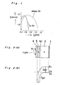
- Fig. 4 shows a schematic sectional view of an HJ solar cell according to a second embodiment of the present invention wherein a crystalline semiconductor region 2' is a thin film.
- a substrate 6 is an thin plate of inorganic solid such as metal, glass or ceramics, or a film of organic solid such as a polyimide.
- An electrode 1' applied on the substrate 6 forms an ohmic contact with a p-type crystalline thin film 2', which is further deposited thereon by using such a process as a chemical vapor deposition (CVD) process, a metal-organic CVD (MOCVD) process, a molecular beam epitaxy (MBE) process, a sputtering process or an ion plating process.
- CVD chemical vapor deposition
- MOCVD metal-organic CVD
- MBE molecular beam epitaxy
- the n-type microcrystalline or amorphous silicon thin film 3 is deposited onto the crystalline semiconductor 2' by using the GD process.
- the transparent conductive film 4 and the comb-like electrode 5 are applied on the thin film 3 in succession in a similar method as in the first embodiment of the present invention.
- the substrate 6 consists of a metallic material, it serves also as an ohmic electrode and it may not be necessary to use the electrode 1' separately.
- the crystalline semiconductor 2' as well as the region 3 are prepared by using the thin film process so that the manufacturing cost of the solar cell can be lowered further than that of the first embodiment of the present invention.
- a crystalline film 2' is made of expensive materials such as GaAs and Ge, which can absorb sunlight in the form of thin films less than several micrometer, the present invention may be more effective to provide a solar cell of high performance at a lower cost. If such a process as the CVD and MOCVD process which are suitable for forming a large-area film is adopted to deposit a crystalline semiconductor 2', a device having a large light-receiving area may be manufactured.
- Fig. 5 (A) shows a photovoltaic device according to a third embodiment of the present invention wherein an HJ solar cell C and an amorphous solar cell A are connected in series.
- the first solar cell C comprises a p-type wafer 2 of polycrystalline silicon and an n-type region 3 of amorphous or microcrystalline silicon which form an HJ
- the second cell A comprises a p-type region 21, an i-type region 22, and an n-type region 23 of amorphous or microcrystalline silicon which form a p-i-n junction.
- An aluminum electrode 1 is deposited on the p-type semiconductor 2, while a transparent conductive film 4 of ITO and an comb-like electrode 5 is applied in succession on the n-type semiconductor 23.
- the thicknesses of those amorphous regions and ITO 3, 21, 22, 23 and 4 are about 3000, 500, 5000, 100 and 700 A, respectively. It should be noted that the crystalline film may be substituted for a crystalline wafer 2; a substrate as used in the second embodiment is needed in case of such a substitution. It should also be noted that the type of conduction in the semiconductor regions may be reversed.
- Fig. 5(B) shows a schematic energy band diagram of the photovoltaic device shown in Fig. 5(A).
- An energy gap E gc of the p-type polycrystalline silicon 2, about 1.1 eV, is smaller than that E g a of the i-type amorphous layer 22 which mainly generates photocarriers in the second cell A, about 1.7-1.8 eV.
- the third embodiment of the present invention is characterized in that an ohmic contact is realized easily at an amorphous p-n junction by the use of a unique characteristic of an amorphous semiconductor that many localized states exist in the forbidden band, though the characteristic is disadvantageous in most cases.
- the absorption of light creates electron-hole pairs as shown in Fig. 5(B).
- the amorphous p-n junction serves as an ohmic junction (OJ).
- Fig. 6 is a graph showing the collection efficiency n of the amorphous silicon solar cell C (a-Si) and of the H-J solar cell (poly-Si) shown in Fig. 2(A), covered with a 0 filter of amorphous silicon having a thickness of 6000 A, plotted against the wavelength X of the incident light.
- the latter data poly-Si can be considered to be almost equal to the collection efficiency of the HJ solar cell C composing the tandem solar cell shown in Fig. 5(A).
- the spectrum curve of the solar energy is shown for reference as the chain line Sun-S in relative amplitude. Since the photovoltaic device shown in Fig. 5 (A) comprises two types of materials with different light-sensitivity, as shown in Fig.
- Fig. 7 shows the data of the I-V characteristics of the photovoltaic device shown in Fig. 5(A).
- the conversion efficiency obtained from the data is 11-12%, which is higher than that exhibited by the prior art amorphous solar cells, i. e., 7 to 8% in general.
- Fig. 8 (A) is a schematic sectional view of a photovoltaic device according to a forth embodiment of the present invention.
- Two amorphous solar cells Al and A2 are formed by depositing amorphous materials successively by means of the GD process on an HJ solar cell C described with reference to Fig. 3, to result in a tandem solar battery.
- the three unitary cells are connected in series.
- a substrate 2 is made of a thin plate of inorganic material such as metal, glass or ceramics, or of a film of organic solid such as a polyimide.
- An ohmic electrode 1 is deposited on the substrate 2, and a p-type crystalline 41 and an n-type amorphous region 42 are deposited further in succession to form a crystalline cell C.
- a p-type region 21, an i-type region 22 and an n-type region 23 of amorphous silicon are deposited on the n-type region 42 to form a second cell A1.
- a p-type region 31, an i-type region 32 and an n-type region 33 of amorphous silicon carbide are deposited on the n-type amorphous silicon 22 in succession to form a third cell A2.
- the junctions between the cells comprising a p-type and an n-type amorphous material provide an ohmic contact.
- a transparent conductive film 4 of ITO and a comb-like electrode 5 are deposited in succession on the semiconductor 33. It should be noted that a crystalline wafer may be substituted for a crystalline thin film 41 in the cell C; the substrate 2 is needless in case of such a substitution. It should also be noted that the type of conduction in the semiconductor regions may be reversed.
- Fib. 8(B) shows a schematic energy band diagram of the photovoltaic device shown in Fig. 8(A), wherein the energy gap E gc of the crystalline GaAs in the cell C is about 1.4 eV, the energy gap Eg al of the i-type amorphous silicon 22 in the first amorphous cell Al larger than E g c is about 1.8 eV, and the energy gap E ga2 of the i-type amorphous silicon carbide 32 larger than E gal is about 2.0 eV.
- the incident light first enters the cell A2 with the largest energy gap Eg a2 , and light of shorter wavelength is absorbed thereby; the light transmitted through the cell A2 is absorbed in the next cell A1 with the energy gap E gal ; finally, the light of longer wavelength transmitted through the cell A1 is absorbed in the cell C with the smallest energy gap E gc .
- solar energy of shorter wavelength may be absorbed in the amorphous solar cells Al and A2 with p-i-n junctions, and that of longer wavelength may be absorbed by the HJ solar cell C with a p-n HJ. Then, high conversion efficiency of a solar battery can be realized.
- Fig. 9 (A) shows a schematic sectional view of a photovoltaic device according to a fifth embodiment of the present invention.
- a tandem solar battery is constructed from two HJ solar cells Cl and C2 connected together in series with the intervention of an amorphous semiconductor region 11 whose type of conduction is controlled to have the same sign as those in a crystalline semiconductor region 12 to provide an ohmic contact between them.
- a solar cell Cl similar to that in Fig. 2(A), comprises a p-type crystalline semiconductor wafer 2 with an energy gap E gc1 and an n-type microcrystalline or amorphous layer 3 with an energy gap E g al larger than E gc1 ; both layers 2 and 3 form a p-n HJ.
- the wafer 2 may be substituted for by a crystalline semiconductor thin film.
- the p-type amorphous layer 11 is deposited on the amorphous layer 3.
- the p-type crystalline semiconductor 12 having an energy gap Eg c2 larger than Eg cl and an n-type amorphous crystalline semiconductor 13 having an energy gap Eg a2 larger than Eg c2 are deposited on the semiconductor 11 in succession.
- the second solar cell C2 comprises the semiconductor regions 12 and 13 which form a p-n HJ.
- solar energy of shorter wavelength is absorbed in the solar cell C2 with a larger energy gap adjoining to the transparent electrode 4, and then solar energy with longer wavelength may be absorbed in the solar cell Cl with a narrower gap. Then, a high conversion efficiency solar battery may be realized at a low manufacturing cost.
- Fig. 10 shows a schematic sectional view of a photovoltaic device of the sixth embodiment according to a present invention. It is constructed by connecting the two HJ solar cells Cl and C2 and the two amorphous solar cells Al and A2 in series.
- numerals 1 to 5 and 11 to 13 represent like parts shown in Fig. 5(A)
- numerals 21 to 23 and 31 to 33 represent like parts shown in Fig. 8(A).
- Fig. 11 shows schematically a photovoltaic device according to a seventh embodiment of the present invention. It comprises six cells connected in series. Three of them are HJ solar cells C1 to C3, and the others are amorphous cells A1 to A3. These cells are connected in series and are applied on a stainless steel substrate 1 with the heterojunction formed around the interface between cells C3 and A1.
- the stainless steel substrate 1 serves also as an electrode.
- the transparent conductive layer 4 and the comb-like electrode 5 are applied in succession on the cell A3.
- the crystalline semiconductor regions in the three HJ cells Cl, C2 and C3 are made from germanium, silicon and GaAs, respectively, and the energy gap E gc1 , E gc2 and E gc3 in the crystalline region are 0.7, 1.1 and 1.4 eV, respectively.
- the three amorphous cells A1, A2 and A3 are made from amorphous silicon germanide, amorphous silicon and amorphous silicon carbide, respectively, and the energy gap E ga1 , E ga2 and E ga3 are 1.6, 1.8 and 2.0 eV, respectively.
- Ohmic contacts are provided at the interfaces between the cells.
- Light of shorter wavelength is absorbed in the third amorphous cell A3 with the largest energy gap Eg a3 situated adjoining to the light-receiving surface 4 through which the light enters.
- the light transmits through the cells applied in one another in series in the order of the energy gap, the light is absorbed successively from at shorter wavelength to at longer wavelength.
- light in a wide range may be utilized in a single device.
- Fig. 12(A) shows a schematic model of a crystalline wafer 2 having an irregular surface designed so as to increase the absorption of the incident light.
- a number of small pyramid-shaped protrusions are formed on the surface of a crystalline semiconductor wafer 2 or of a thin plate made of an inorganic or organic solid.
- a photovoltaic cell according to all the embodiments of the present invention may be manufactured by depositing materials on a substrate of this type.
- a part of the photovoltaic device in the third embodiment manufactured by successive deposition on the substrate shown in Fig. 12(A) is shown in sectional representation in Fig. 12(B) wherein 4 designates a transparent conductive film, A an amorphous solar cell and C an H-J solar cell.
- An incident light transmitted through the conductive layer 4 is reflected partially at the interface between the transparent conductive layer 4 and the amorphous region 21, and between the semiconductors 2 and 3.
- the solid line in Fig. 12(B) indicates the confinement of light in the semiconductor layer 2.
- the confinement effect caused by the multiple reflection may increase the conversion efficiency by enhancing the absorption of the incident light.
- a photovoltaic device having a tandem structures disclosed in the third to seventh embodiments can be used not only as a solar cell but also as a photodetector by using the different photosensitivities of unitary cells composing the photovoltaic device.
Applications Claiming Priority (4)
| Application Number | Priority Date | Filing Date | Title |
|---|---|---|---|
| JP57234197A JPH0644638B2 (ja) | 1982-12-29 | 1982-12-29 | 異質単位セル同士のスタック形光起電力素子 |
| JP234197/82 | 1982-12-29 | ||
| JP58049318A JPS59175170A (ja) | 1983-03-24 | 1983-03-24 | タンデム型太陽電池 |
| JP49318/83 | 1983-03-24 |
Publications (3)
| Publication Number | Publication Date |
|---|---|
| EP0113434A1 true EP0113434A1 (fr) | 1984-07-18 |
| EP0113434B1 EP0113434B1 (fr) | 1989-04-05 |
| EP0113434B2 EP0113434B2 (fr) | 1995-08-30 |
Family
ID=26389698
Family Applications (1)
| Application Number | Title | Priority Date | Filing Date |
|---|---|---|---|
| EP83112159A Expired - Lifetime EP0113434B2 (fr) | 1982-12-29 | 1983-12-02 | Dispositif photovoltaique |
Country Status (3)
| Country | Link |
|---|---|
| US (1) | US4496788A (fr) |
| EP (1) | EP0113434B2 (fr) |
| DE (1) | DE3379565D1 (fr) |
Cited By (14)
| Publication number | Priority date | Publication date | Assignee | Title |
|---|---|---|---|---|
| DE3516117A1 (de) * | 1985-05-04 | 1986-11-06 | Telefunken electronic GmbH, 7100 Heilbronn | Solarzelle |
| DE3614546A1 (de) * | 1984-10-29 | 1987-11-05 | Mitsubishi Electric Corp | Amorphe solarzelle |
| FR2615327A1 (fr) * | 1987-03-27 | 1988-11-18 | Sanyo Electric Co | Dispositif photovoltaique |
| FR2650916A1 (fr) * | 1989-08-09 | 1991-02-15 | Sanyo Electric Co | Dispositif photovoltaique |
| DE4116695A1 (de) * | 1990-05-23 | 1991-12-12 | Mitsubishi Electric Corp | Solarzelle und herstellungsverfahren fuer dieselbe |
| US5288338A (en) * | 1990-05-23 | 1994-02-22 | Mitsubishi Denki Kabushiki Kaisha | Solar cell and method of producing the solar cell |
| EP0622811A1 (fr) * | 1993-04-21 | 1994-11-02 | Nazir P. Kherani | Batteries nucléaires |
| DE4143408C2 (de) * | 1990-05-23 | 1994-11-17 | Mitsubishi Electric Corp | Verfahren zur Herstellung einer Solarzelle |
| WO2001057933A1 (fr) * | 2000-02-04 | 2001-08-09 | Kaneka Corporation | Transducteur photoelectrique a couche mince hybride, et lamine transparent destine audit transducteur |
| US6297443B1 (en) | 1997-08-21 | 2001-10-02 | Kaneka Corporation | Thin film photoelectric transducer |
| WO2003083953A1 (fr) * | 2002-03-29 | 2003-10-09 | Ebara Corporation | Pile solaire et procede permettant de la produire |
| US8076175B2 (en) | 2008-02-25 | 2011-12-13 | Suniva, Inc. | Method for making solar cell having crystalline silicon P-N homojunction and amorphous silicon heterojunctions for surface passivation |
| WO2013050257A3 (fr) * | 2011-10-07 | 2013-09-06 | Ewe-Forschungszentrum Für Energietechnologie E. V. | Cellule solaire multijonction photovoltaïque |
| EP2105972A3 (fr) * | 2008-03-28 | 2015-06-10 | Semiconductor Energy Laboratory Co, Ltd. | Dispositif de conversion photoélectrique et procédé de fabrication de celui-ci |
Families Citing this family (78)
| Publication number | Priority date | Publication date | Assignee | Title |
|---|---|---|---|---|
| US4536607A (en) * | 1984-03-01 | 1985-08-20 | Wiesmann Harold J | Photovoltaic tandem cell |
| US4609771A (en) * | 1984-11-02 | 1986-09-02 | Sovonics Solar Systems | Tandem junction solar cell devices incorporating improved microcrystalline p-doped semiconductor alloy material |
| US4600801A (en) * | 1984-11-02 | 1986-07-15 | Sovonics Solar Systems | Fluorinated, p-doped microcrystalline silicon semiconductor alloy material |
| US4745446A (en) * | 1985-02-11 | 1988-05-17 | American Telephone And Telegraph Company, At&T Bell Laboratories | Photodetector and amplifier integration |
| JPH0712100B2 (ja) * | 1985-03-25 | 1995-02-08 | 株式会社日立製作所 | 半導体発光素子 |
| US4923524A (en) * | 1985-05-06 | 1990-05-08 | Chronar Corp. | Wide ranging photovoltaic laminates comprising particulate semiconductors |
| JPS63182551U (fr) * | 1987-05-15 | 1988-11-24 | ||
| US5103284A (en) * | 1991-02-08 | 1992-04-07 | Energy Conversion Devices, Inc. | Semiconductor with ordered clusters |
| JPH04275467A (ja) * | 1991-03-04 | 1992-10-01 | Sanyo Electric Co Ltd | フォトトランジスタ |
| US5808233A (en) * | 1996-03-11 | 1998-09-15 | Temple University-Of The Commonwealth System Of Higher Education | Amorphous-crystalline thermocouple and methods of its manufacture |
| AU2002303658A1 (en) * | 2001-05-08 | 2002-11-18 | Kimerling, Lionel, C. | Silicon solar cell with germanium backside solar cell |
| US7026596B2 (en) * | 2003-10-30 | 2006-04-11 | Micron Technology, Inc. | High-low sensitivity pixel |
| JP4969785B2 (ja) * | 2005-02-16 | 2012-07-04 | 本田技研工業株式会社 | カルコパイライト型太陽電池及びその製造方法 |
| US7554031B2 (en) * | 2005-03-03 | 2009-06-30 | Sunpower Corporation | Preventing harmful polarization of solar cells |
| US20060207647A1 (en) * | 2005-03-16 | 2006-09-21 | General Electric Company | High efficiency inorganic nanorod-enhanced photovoltaic devices |
| US20070169808A1 (en) * | 2006-01-26 | 2007-07-26 | Kherani Nazir P | Solar cell |
| EP2047522A2 (fr) * | 2006-07-21 | 2009-04-15 | Koninklijke Philips Electronics N.V. | Photodiode de détection dans un diagnostic moléculaire |
| US20080110486A1 (en) * | 2006-11-15 | 2008-05-15 | General Electric Company | Amorphous-crystalline tandem nanostructured solar cells |
| US20080160024A1 (en) * | 2006-12-07 | 2008-07-03 | Board Of Trustees Of The University Of Arkansas | Inhibition of cancer metastasis |
| DE102007009924A1 (de) * | 2007-02-27 | 2008-08-28 | Carl Zeiss Laser Optics Gmbh | Durchlaufbeschichtungsanlage, Verfahren zur Herstellung kristalliner Dünnschichten und Solarzellen sowie Solarzelle |
| CN101622722B (zh) * | 2007-02-27 | 2012-11-21 | 卡尔蔡司激光器材有限责任公司 | 连续涂覆设备、生产晶态薄膜和太阳电池的方法 |
| KR20090028883A (ko) * | 2007-09-17 | 2009-03-20 | 주성엔지니어링(주) | 태양전지 및 그 제조방법 |
| US7851249B2 (en) * | 2007-10-31 | 2010-12-14 | Atomic Energy Council - Institute Of Nuclear Energy Research | Tandem solar cell including an amorphous silicon carbide layer and a multi-crystalline silicon layer |
| US20090293955A1 (en) * | 2007-11-07 | 2009-12-03 | Qualcomm Incorporated | Photovoltaics with interferometric masks |
| KR101608953B1 (ko) * | 2007-11-09 | 2016-04-04 | 가부시키가이샤 한도오따이 에네루기 켄큐쇼 | 광전 변환 장치 및 그 제조 방법 |
| EP2618387A1 (fr) * | 2007-11-09 | 2013-07-24 | Sunpreme Inc. | Piles solaires à faible coût et leurs procédés de production |
| TWI452703B (zh) * | 2007-11-16 | 2014-09-11 | Semiconductor Energy Lab | 光電轉換裝置及其製造方法 |
| US20090131730A1 (en) * | 2007-11-16 | 2009-05-21 | Lun-Teh Yuen | Oxygenate conversion using boron-containing molecular sieve cha |
| US20090139558A1 (en) * | 2007-11-29 | 2009-06-04 | Shunpei Yamazaki | Photoelectric conversion device and manufacturing method thereof |
| JP5248995B2 (ja) * | 2007-11-30 | 2013-07-31 | 株式会社半導体エネルギー研究所 | 光電変換装置の製造方法 |
| JP5248994B2 (ja) * | 2007-11-30 | 2013-07-31 | 株式会社半導体エネルギー研究所 | 光電変換装置の製造方法 |
| JP5572307B2 (ja) * | 2007-12-28 | 2014-08-13 | 株式会社半導体エネルギー研究所 | 光電変換装置の製造方法 |
| EP2075850A3 (fr) * | 2007-12-28 | 2011-08-24 | Semiconductor Energy Laboratory Co, Ltd. | Dispositif de conversion photoélectrique et son procédé de fabrication |
| DE102008006987A1 (de) * | 2008-01-31 | 2009-08-06 | Osram Opto Semiconductors Gmbh | Strahlungsempfänger und Verfahren zur Herstellung eines Strahlungsempfängers |
| US8129613B2 (en) * | 2008-02-05 | 2012-03-06 | Twin Creeks Technologies, Inc. | Photovoltaic cell comprising a thin lamina having low base resistivity and method of making |
| US20090211623A1 (en) * | 2008-02-25 | 2009-08-27 | Suniva, Inc. | Solar module with solar cell having crystalline silicon p-n homojunction and amorphous silicon heterojunctions for surface passivation |
| US20090211627A1 (en) * | 2008-02-25 | 2009-08-27 | Suniva, Inc. | Solar cell having crystalline silicon p-n homojunction and amorphous silicon heterojunctions for surface passivation |
| US7947523B2 (en) * | 2008-04-25 | 2011-05-24 | Semiconductor Energy Laboratory Co., Ltd. | Method for manufacturing photoelectric conversion device |
| US7951656B2 (en) * | 2008-06-06 | 2011-05-31 | Semiconductor Energy Laboratory Co., Ltd. | Method for manufacturing semiconductor device |
| US8338218B2 (en) * | 2008-06-26 | 2012-12-25 | Semiconductor Energy Laboratory Co., Ltd. | Photoelectric conversion device module and manufacturing method of the photoelectric conversion device module |
| US8338209B2 (en) * | 2008-08-10 | 2012-12-25 | Twin Creeks Technologies, Inc. | Photovoltaic cell comprising a thin lamina having a rear junction and method of making |
| US20100032010A1 (en) * | 2008-08-10 | 2010-02-11 | Twin Creeks Technologies, Inc. | Method to mitigate shunt formation in a photovoltaic cell comprising a thin lamina |
| US20100096006A1 (en) * | 2008-10-16 | 2010-04-22 | Qualcomm Mems Technologies, Inc. | Monolithic imod color enhanced photovoltaic cell |
| US7858427B2 (en) * | 2009-03-03 | 2010-12-28 | Applied Materials, Inc. | Crystalline silicon solar cells on low purity substrate |
| TWI379430B (en) * | 2009-04-16 | 2012-12-11 | Atomic Energy Council | A method of fabricating a thin interface for internal light reflection and impurities isolation |
| KR101039156B1 (ko) * | 2009-04-30 | 2011-06-03 | 한양대학교 산학협력단 | 탄소나노튜브층을 포함하는 태양전지 |
| US8188363B2 (en) | 2009-08-07 | 2012-05-29 | Sunpower Corporation | Module level solutions to solar cell polarization |
| US7928389B1 (en) | 2009-08-20 | 2011-04-19 | Hrl Laboratories, Llc | Wide bandwidth infrared detector and imager |
| US7977637B1 (en) | 2009-08-20 | 2011-07-12 | Hrl Laboratories, Llc | Honeycomb infrared detector |
| US8946839B1 (en) | 2009-08-20 | 2015-02-03 | Hrl Laboratories, Llc | Reduced volume infrared detector |
| US20110048505A1 (en) * | 2009-08-27 | 2011-03-03 | Gabriela Bunea | Module Level Solution to Solar Cell Polarization Using an Encapsulant with Opened UV Transmission Curve |
| US20110088763A1 (en) * | 2009-10-15 | 2011-04-21 | Applied Materials, Inc. | Method and apparatus for improving photovoltaic efficiency |
| JP5706670B2 (ja) | 2009-11-24 | 2015-04-22 | 株式会社半導体エネルギー研究所 | Soi基板の作製方法 |
| TW201133881A (en) * | 2010-03-22 | 2011-10-01 | Auria Solar Co Ltd | Thin film solar cell and manufacturing method thereof |
| TWI408823B (zh) * | 2010-06-11 | 2013-09-11 | An Ching New Energy Machinery & Equipment Co Ltd | The solar cell structure of Sanhuan semiconductor and its manufacturing method |
| TW201145546A (en) * | 2010-06-15 | 2011-12-16 | An Ching New Energy Machinery & Equipment Co Ltd | Solar cell structure with high electro-optic conversion efficiency and manufacturing method thereof |
| JP5753445B2 (ja) | 2010-06-18 | 2015-07-22 | 株式会社半導体エネルギー研究所 | 光電変換装置 |
| US8377738B2 (en) | 2010-07-01 | 2013-02-19 | Sunpower Corporation | Fabrication of solar cells with counter doping prevention |
| CN102479849A (zh) * | 2010-11-24 | 2012-05-30 | 吉富新能源科技(上海)有限公司 | 具有高光电转换效率的太阳能电池结构及其制作方法 |
| CN102479848A (zh) * | 2010-11-24 | 2012-05-30 | 吉富新能源科技(上海)有限公司 | 三五族半导体的太阳能电池结构及其制作方法 |
| US9437758B2 (en) | 2011-02-21 | 2016-09-06 | Semiconductor Energy Laboratory Co., Ltd. | Photoelectric conversion device |
| KR20120119807A (ko) * | 2011-04-22 | 2012-10-31 | 삼성전자주식회사 | 태양 전지 |
| US9099596B2 (en) * | 2011-07-29 | 2015-08-04 | International Business Machines Corporation | Heterojunction photovoltaic device and fabrication method |
| JP2013058562A (ja) | 2011-09-07 | 2013-03-28 | Semiconductor Energy Lab Co Ltd | 光電変換装置 |
| US9373741B2 (en) * | 2012-08-15 | 2016-06-21 | International Business Machines Corporation | Heterostructure germanium tandem junction solar cell |
| US9812590B2 (en) | 2012-10-25 | 2017-11-07 | Sunpower Corporation | Bifacial solar cell module with backside reflector |
| US9035172B2 (en) | 2012-11-26 | 2015-05-19 | Sunpower Corporation | Crack resistant solar cell modules |
| US9306106B2 (en) | 2012-12-18 | 2016-04-05 | International Business Machines Corporation | Monolithic integration of heterojunction solar cells |
| KR20140082012A (ko) * | 2012-12-21 | 2014-07-02 | 엘지전자 주식회사 | 태양 전지 및 이의 제조 방법 |
| US8796061B2 (en) | 2012-12-21 | 2014-08-05 | Sunpower Corporation | Module assembly for thin solar cells |
| US10903261B1 (en) | 2013-03-15 | 2021-01-26 | Hrl Laboratories, Llc | Triple output, dual-band detector |
| US9490292B1 (en) | 2013-03-15 | 2016-11-08 | Hrl Laboratories, Llc | Dual-band detector array |
| KR20140135881A (ko) * | 2013-05-16 | 2014-11-27 | 엘지전자 주식회사 | 태양 전지 및 이의 제조 방법 |
| US9685571B2 (en) | 2013-08-14 | 2017-06-20 | Sunpower Corporation | Solar cell module with high electric susceptibility layer |
| DE102015015017A1 (de) | 2015-11-19 | 2017-05-24 | Institut Für Solarenergieforschung Gmbh | Solarzelle und Verfahren zur Herstellung einer Solarzelle mit mehreren durch ladungsträgerselektive Kontakte miteinander verbundenen Absorbern |
| JP6554230B2 (ja) | 2016-04-07 | 2019-07-31 | 株式会社カネカ | 多接合光電変換装置の製造方法 |
| US10020331B1 (en) | 2016-07-21 | 2018-07-10 | Hrl Laboratories, Llc | Dual-band lateral-effect position sensor |
| JP6782211B2 (ja) * | 2017-09-08 | 2020-11-11 | 株式会社東芝 | 透明電極、それを用いた素子、および素子の製造方法 |
Citations (4)
| Publication number | Priority date | Publication date | Assignee | Title |
|---|---|---|---|---|
| US4016586A (en) | 1974-03-27 | 1977-04-05 | Innotech Corporation | Photovoltaic heterojunction device employing a wide bandgap material as an active layer |
| US4253882A (en) | 1980-02-15 | 1981-03-03 | University Of Delaware | Multiple gap photovoltaic device |
| US4272641A (en) * | 1979-04-19 | 1981-06-09 | Rca Corporation | Tandem junction amorphous silicon solar cells |
| US4292461A (en) * | 1980-06-20 | 1981-09-29 | International Business Machines Corporation | Amorphous-crystalline tandem solar cell |
Family Cites Families (4)
| Publication number | Priority date | Publication date | Assignee | Title |
|---|---|---|---|---|
| JPS55125680A (en) * | 1979-03-20 | 1980-09-27 | Yoshihiro Hamakawa | Photovoltaic element |
| US4270018A (en) * | 1979-12-26 | 1981-05-26 | Gibbons James F | Amorphous solar cells |
| US4377723A (en) * | 1980-05-02 | 1983-03-22 | The University Of Delaware | High efficiency thin-film multiple-gap photovoltaic device |
| JPS5749278A (en) * | 1980-09-08 | 1982-03-23 | Mitsubishi Electric Corp | Amorphous silicone solar cell |
-
1983
- 1983-09-02 US US06/528,988 patent/US4496788A/en not_active Expired - Lifetime
- 1983-12-02 EP EP83112159A patent/EP0113434B2/fr not_active Expired - Lifetime
- 1983-12-02 DE DE8383112159T patent/DE3379565D1/de not_active Expired
Patent Citations (4)
| Publication number | Priority date | Publication date | Assignee | Title |
|---|---|---|---|---|
| US4016586A (en) | 1974-03-27 | 1977-04-05 | Innotech Corporation | Photovoltaic heterojunction device employing a wide bandgap material as an active layer |
| US4272641A (en) * | 1979-04-19 | 1981-06-09 | Rca Corporation | Tandem junction amorphous silicon solar cells |
| US4253882A (en) | 1980-02-15 | 1981-03-03 | University Of Delaware | Multiple gap photovoltaic device |
| US4292461A (en) * | 1980-06-20 | 1981-09-29 | International Business Machines Corporation | Amorphous-crystalline tandem solar cell |
Non-Patent Citations (1)
| Title |
|---|
| APPLIED PHYSICS LETTERS, vol. 34, no. 1, 1 January 1979, New York S.M. BEDAIR et al. "A two-junction cascade solar-cell structure", pages 38-39 * |
Cited By (15)
| Publication number | Priority date | Publication date | Assignee | Title |
|---|---|---|---|---|
| DE3614546A1 (de) * | 1984-10-29 | 1987-11-05 | Mitsubishi Electric Corp | Amorphe solarzelle |
| DE3516117A1 (de) * | 1985-05-04 | 1986-11-06 | Telefunken electronic GmbH, 7100 Heilbronn | Solarzelle |
| FR2615327A1 (fr) * | 1987-03-27 | 1988-11-18 | Sanyo Electric Co | Dispositif photovoltaique |
| FR2650916A1 (fr) * | 1989-08-09 | 1991-02-15 | Sanyo Electric Co | Dispositif photovoltaique |
| DE4143408C2 (de) * | 1990-05-23 | 1994-11-17 | Mitsubishi Electric Corp | Verfahren zur Herstellung einer Solarzelle |
| DE4116695A1 (de) * | 1990-05-23 | 1991-12-12 | Mitsubishi Electric Corp | Solarzelle und herstellungsverfahren fuer dieselbe |
| US5288338A (en) * | 1990-05-23 | 1994-02-22 | Mitsubishi Denki Kabushiki Kaisha | Solar cell and method of producing the solar cell |
| EP0622811A1 (fr) * | 1993-04-21 | 1994-11-02 | Nazir P. Kherani | Batteries nucléaires |
| US6297443B1 (en) | 1997-08-21 | 2001-10-02 | Kaneka Corporation | Thin film photoelectric transducer |
| WO2001057933A1 (fr) * | 2000-02-04 | 2001-08-09 | Kaneka Corporation | Transducteur photoelectrique a couche mince hybride, et lamine transparent destine audit transducteur |
| US6759645B2 (en) | 2000-02-04 | 2004-07-06 | Kaneka Corporation | Hybrid thin-film photoelectric transducer and transparent laminate for the transducer |
| WO2003083953A1 (fr) * | 2002-03-29 | 2003-10-09 | Ebara Corporation | Pile solaire et procede permettant de la produire |
| US8076175B2 (en) | 2008-02-25 | 2011-12-13 | Suniva, Inc. | Method for making solar cell having crystalline silicon P-N homojunction and amorphous silicon heterojunctions for surface passivation |
| EP2105972A3 (fr) * | 2008-03-28 | 2015-06-10 | Semiconductor Energy Laboratory Co, Ltd. | Dispositif de conversion photoélectrique et procédé de fabrication de celui-ci |
| WO2013050257A3 (fr) * | 2011-10-07 | 2013-09-06 | Ewe-Forschungszentrum Für Energietechnologie E. V. | Cellule solaire multijonction photovoltaïque |
Also Published As
| Publication number | Publication date |
|---|---|
| US4496788A (en) | 1985-01-29 |
| DE3379565D1 (en) | 1989-05-11 |
| EP0113434B1 (fr) | 1989-04-05 |
| EP0113434B2 (fr) | 1995-08-30 |
Similar Documents
| Publication | Publication Date | Title |
|---|---|---|
| US4496788A (en) | Photovoltaic device | |
| EP0523919B1 (fr) | Dispositif photovoltaique à multijonction et méthode de fabrication | |
| EP0494088B1 (fr) | Dispositif photovoltaique | |
| US7879644B2 (en) | Hybrid window layer for photovoltaic cells | |
| JP2999280B2 (ja) | 光起電力素子 | |
| JP2719230B2 (ja) | 光起電力素子 | |
| US6368892B1 (en) | Monolithic multi-junction solar cells with amorphous silicon and CIS and their alloys | |
| US5066340A (en) | Photovoltaic device | |
| US5256887A (en) | Photovoltaic device including a boron doping profile in an i-type layer | |
| EP0213622A2 (fr) | Eléments photovoltaiques amorphes | |
| US20030079771A1 (en) | Stacked photovoltaic device | |
| EP2136413A2 (fr) | Dispositif photovoltaïque | |
| EP0179896A1 (fr) | Cellules solaires et photodetecteurs | |
| US5103851A (en) | Solar battery and method of manufacturing the same | |
| US20030217769A1 (en) | Stacked photovoltaic element | |
| EP0248953A1 (fr) | Piles solaires en cascade | |
| Carlson | Solar cells | |
| JPH11150282A (ja) | 光起電力素子及びその製造方法 | |
| JP2001028452A (ja) | 光電変換装置 | |
| JPS636882A (ja) | タンデム構成の光電池装置 | |
| Compaan | Materials challenges for terrestrial thin-film photovoltaics | |
| JPH0927630A (ja) | 光起電力素子及びその製造方法 | |
| JP2757896B2 (ja) | 光起電力装置 | |
| JPH0927632A (ja) | 光起電力素子及びその製造方法 | |
| Böer et al. | Solar cells |
Legal Events
| Date | Code | Title | Description |
|---|---|---|---|
| PUAI | Public reference made under article 153(3) epc to a published international application that has entered the european phase |
Free format text: ORIGINAL CODE: 0009012 |
|
| AK | Designated contracting states |
Designated state(s): DE FR GB |
|
| 17P | Request for examination filed |
Effective date: 19840907 |
|
| RAP1 | Party data changed (applicant data changed or rights of an application transferred) |
Owner name: DAIHEN CORPORATION Owner name: OKAMOTO, HIROAKI Owner name: HAMAKAWA, YOSHIHIRO |
|
| GRAA | (expected) grant |
Free format text: ORIGINAL CODE: 0009210 |
|
| AK | Designated contracting states |
Kind code of ref document: B1 Designated state(s): DE FR GB |
|
| REF | Corresponds to: |
Ref document number: 3379565 Country of ref document: DE Date of ref document: 19890511 |
|
| ET | Fr: translation filed | ||
| PLBI | Opposition filed |
Free format text: ORIGINAL CODE: 0009260 |
|
| 26 | Opposition filed |
Opponent name: BSG TECHNISCHE BERATUNGS-GESELLSCHAFT MBH Effective date: 19900104 |
|
| PLAB | Opposition data, opponent's data or that of the opponent's representative modified |
Free format text: ORIGINAL CODE: 0009299OPPO |
|
| R26 | Opposition filed (corrected) |
Opponent name: BSG TECHNISCHE BERATUNGS-GESELLSCHAFT MBH Effective date: 19900104 |
|
| PUAH | Patent maintained in amended form |
Free format text: ORIGINAL CODE: 0009272 |
|
| STAA | Information on the status of an ep patent application or granted ep patent |
Free format text: STATUS: PATENT MAINTAINED AS AMENDED |
|
| 27A | Patent maintained in amended form |
Effective date: 19950830 |
|
| AK | Designated contracting states |
Kind code of ref document: B2 Designated state(s): DE FR GB |
|
| ET3 | Fr: translation filed ** decision concerning opposition | ||
| REG | Reference to a national code |
Ref country code: GB Ref legal event code: IF02 |
|
| PGFP | Annual fee paid to national office [announced via postgrant information from national office to epo] |
Ref country code: GB Payment date: 20021127 Year of fee payment: 20 |
|
| PGFP | Annual fee paid to national office [announced via postgrant information from national office to epo] |
Ref country code: DE Payment date: 20021205 Year of fee payment: 20 |
|
| PGFP | Annual fee paid to national office [announced via postgrant information from national office to epo] |
Ref country code: FR Payment date: 20021210 Year of fee payment: 20 |
|
| PG25 | Lapsed in a contracting state [announced via postgrant information from national office to epo] |
Ref country code: GB Free format text: LAPSE BECAUSE OF EXPIRATION OF PROTECTION Effective date: 20031201 |
|
| REG | Reference to a national code |
Ref country code: GB Ref legal event code: PE20 |