EP0112831B1 - Fast packet switch - Google Patents
Fast packet switch Download PDFInfo
- Publication number
- EP0112831B1 EP0112831B1 EP83900462A EP83900462A EP0112831B1 EP 0112831 B1 EP0112831 B1 EP 0112831B1 EP 83900462 A EP83900462 A EP 83900462A EP 83900462 A EP83900462 A EP 83900462A EP 0112831 B1 EP0112831 B1 EP 0112831B1
- Authority
- EP
- European Patent Office
- Prior art keywords
- packet
- address
- control
- input
- trunk
- Prior art date
- Legal status (The legal status is an assumption and is not a legal conclusion. Google has not performed a legal analysis and makes no representation as to the accuracy of the status listed.)
- Expired
Links
Images


Classifications
-
- H—ELECTRICITY
- H04—ELECTRIC COMMUNICATION TECHNIQUE
- H04L—TRANSMISSION OF DIGITAL INFORMATION, e.g. TELEGRAPHIC COMMUNICATION
- H04L49/00—Packet switching elements
- H04L49/25—Routing or path finding in a switch fabric
- H04L49/253—Routing or path finding in a switch fabric using establishment or release of connections between ports
- H04L49/254—Centralised controller, i.e. arbitration or scheduling
-
- H—ELECTRICITY
- H04—ELECTRIC COMMUNICATION TECHNIQUE
- H04L—TRANSMISSION OF DIGITAL INFORMATION, e.g. TELEGRAPHIC COMMUNICATION
- H04L49/00—Packet switching elements
- H04L49/10—Packet switching elements characterised by the switching fabric construction
- H04L49/113—Arrangements for redundant switching, e.g. using parallel planes
- H04L49/118—Address processing within a device, e.g. using internal ID or tags for routing within a switch
-
- H—ELECTRICITY
- H04—ELECTRIC COMMUNICATION TECHNIQUE
- H04L—TRANSMISSION OF DIGITAL INFORMATION, e.g. TELEGRAPHIC COMMUNICATION
- H04L49/00—Packet switching elements
- H04L49/10—Packet switching elements characterised by the switching fabric construction
-
- H—ELECTRICITY
- H04—ELECTRIC COMMUNICATION TECHNIQUE
- H04L—TRANSMISSION OF DIGITAL INFORMATION, e.g. TELEGRAPHIC COMMUNICATION
- H04L49/00—Packet switching elements
- H04L49/30—Peripheral units, e.g. input or output ports
Landscapes
- Engineering & Computer Science (AREA)
- Computer Networks & Wireless Communication (AREA)
- Signal Processing (AREA)
- Data Exchanges In Wide-Area Networks (AREA)
Abstract
Description
- Concurrently filed herewith and assigned to the same assignee as this application are:
- "An Interface Facility for a Packet Switching System", European Patent Application No. 83900465.2;
- "End-to-End Information Memory Arrangement in a Line Controller", European Patent Application No. 83900598.0;
- "Time Stamping for a Packet Switching System", European Patent Application No. 83900516.2 and
- "A Fast Packet Switching Network", European Patent Application No. 83900515.4.
- This invention relates to a packet switch for switching packets of digital signals between a plurality of input terminals and a plurality of output terminals, and said switch comprising, a plurality of input control means each of which is connected to an individual one of said input terminals, as plurality of output control means each of which is connected to an individual one of said output terminals, means individually connecting each of said input control means to each of said output control means.
- The advantages of transmitting data and voice information in packets has long been recognized. Packet switching provides a known solution to problems where the information to be transmitted occurs in short, high-rate bursts, with long pauses between bursts.
- As the number of different applications for packet switching grows, the requirements have become more stringent on packet switching systems. They must be capable of routing the packets to their destination, preferably through the use of an address contained within the packet itself. In addition, the system must provide buffering at different nodes within the system to allow for the temporary storage of packets if the intended route of those packets is temporarily experiencing traffic delays. Many of the emerging applications for packet switching, such as for the switching of digitally encoded voice information, require a packet switching system having thousands of the switching modes. An important goal in the design of such large packet systems is that each node be capable of rapidly switching packets and especially have a reasonable physical size.
- Prior art systems for switching packets have been rather small systems consisting of only a few hundred nodes. In addition, such systems have employed large computers using sophisticated software packages to perform the packet switching functions at the nodes within the system. The systems customarily have used complex control protocols to handle the problems of error recovery and flow control and, as a result, have had a limited packet handling capability of only a few thousand packets per second.
- Typically, in the prior art, when a packet was received, a computer examined the logical address to determine the destination of the packet and then executed the necessary steps to effect a transmission of the packet to that destination. The process involved the time consuming steps at each node of translating the logical address into a physical address of the transmission link over which the packet was to be retransmitted, and then, after receiving and buffering the entire packet, performing error and flow control function followed by actual packet retransmission to a succeeding node. Obviously, such a complicated process results in substantial throughput switching delays and undesirably introduces variable delays at the different switching nodes which culminates in packets arriving out of sequence at their destination.
- "Binary Routing Networks", !FFΓ Transactions on Computers, Vol. C-28, No. 10, October, 1979, (New York, U.S.) A. Hopper, et al., pages 699-703, indicates the possibility of performing address rotation by a packet switching node within a packet switching system. The extent of this disclosure is the statement on page 699 that "to minimize the delay through each node the routing bits can be rotated so that the first bit of the route field always indicates the next field". No further disclosure of rotating the address bits is given in this article or how such rotation would be implemented.
- U.S. Patent 4,284,976, describes segment interface circuits for interexchanging packets between a broadcast medium such as optical fibers or satellite communications in a packet switching system. The segment interface circuits are responsive to packets being transmitted on one broadcast medium to transfer these packets to another broadcast medium if the most significant address of the destination address field indicates the packet is intended for the other broadcast medium. Before transferring the packet to the other broadcast medium, the segment interface circuit removes the most significant address from the destination field and places it in the source address field. The segment interface circuitry does not address translation nor does it form a new type of packet.
- "A Packet Network Architecture for Local Interconnection," lCC' 80 Conference Record, Vol. 3, June 1980, (New York, U.S.) S.S. Lam, pages 39.2.1-39.2.6, describes a packet switching network based upon broadcast coaxial cables and is intended as a local network environment.
- U.S. Patent 4,049,906, describes a digital message network for the communication of address coded telegrams between a plurality of subscriber stations. The originating subscriber station transmits a telegram message to a destination subscriber station by first inserting the actual complete physical address necessary to route the telegram through the digital message network to the destination subscriber station. The subscriber station/switching nodes are responsive to telegrams to examine the physical address and to properly route the telegram to the next subscriber station. The patent teaches that as each subscriber station processes its portion of the physical address, it deletes this portion of the physical address so that the physical address becomes shorter and shorter as the telegram proceeds through the network,
column 4, lines 37 through 43. The patent does suggest that another way in which the address could be handled would be to rotate the physical address as it proceeds from the subscriber station to subscriber station, but no disclosure is given of how this would be implemented,column 4, line 35. - "Message Switching Circuits for Multi-Microprocessors," COMPCON 80 Conference Proceedings, IEEE ComputerSociety, February, 1980 (San Francisco, U.S.) C.H. Sequin, pages 331-333, described in Section 3.2 a transmission protocol between switching modes whereby upon receiving each byte of a packet, the receiving node transmits an acknowledge signal back to the transmitting node. Fig. 4 illustrates a timing diagram utilizing this protocol.
- "Prototype X25 Interchange for Use in Local Area Networks," Software and Microsystems, Vol. 1, No. 3, April, 1982, (Camberley, GB), F. Halsall, et al., pages 69-73, decribes a multiprocessor packet switch utilizing the CCITT standard protocol X25.
- "Proposed Organization for Packet Switched Data-Communication Network, "Proceedings of the lEEE, Vol. 119, No. 12, December, 1972, (London, GB) D.H. Beeforth, et al., pages 1677-1682, describes a system which employs adaptive message routing and, in particular, uses a route-switch packet to establish route information at each node within the switching system. The route-search packet is transmitted from an originating terminal to a destination terminals for setting up a route for a message. Each node in response to the route-search packet determines the most suitable link for forwarding the route-search packet to the next node and stores entries in the route list necessary to route subsequent packets of the message. When the route-search packet is received at the destination terminal, the destination terminal transmits a route-reply packet to the destinational terminal over a reverse path of the route. The route address information necessary to communicate subsequent message packets is stored at each node.
- Not only are known prior art systems unable to implement a toll switching network function because of the undesirable switching delay, but the existing structures for switching node architectures heretofore would be physically too large if expanded to perform the toll function. The prior art architectures do not lend themselves well to physical reductions which are possible through the use of very large scale integration (VLSI).
- The problems are solved in accordance with this invention in a packet switching system in which each of said packets comprising an address field of said digital bit signals defining a packet communication path from an individual one of said input control means over said connecting means and an individual one of said output control means to said individual one or said output terminals connected thereto, the input control means comprises, means for storing address and other digital bit signals of a packet received from said individual one of said input terminals and means responsive to a receipt of said address signals for sending a packet communication request signal to the address designated output control means, means for controlling said storing means to commence a transmission therefrom of address and other digital bit signals of said received packet to the one of said output terminals identified by the stored address signals of said packet immediately upon receipt of a packet communication availability signal indicating an idle condition of said defined one of said output terminals.
- A departure in the art is achieved with an integratable high-speed switching network having a plurality of switching nodes interposed between a plurality of input and output conductors and with each such node comprising a circuit responsive to a receipt of a predetermined group of bits in a bit pattern from the input conductors for steering the bit group to a subsequent one of the switching stages or to the output conductors. Each node further comprises a circuit for repositioning the group of bits to a different location in the bit pattern incident to the steering. The steering circuit is responsive to the predetermined group of bits appearing in the most significant bit position of the bit pattern, and the repositioning circuit relocates that group of bits to a less significant bit position of the bit pattern prior to the steering.
- The network architecture comprises interconnected switching nodes and a protocol of operation between those switching nodes which allows for the interchange of signals that determines whether or not a packet can immediately be transmitted to the next sequential switching node without full buffering of the entire packet. The protocol provides that each switching node determines the next sequential switching node illustratively in response to the most significant bits of the address contained in each packet. The protocol utilizes dynamic path availability signaling between cooperating switching nodes to reduce packet buffering delays and increase hhe speed of packet switching through the system.
- Packet buffering delays are reduced by equipping each input of a switching node with a variable length buffer. The latter stores a portion of an incoming packet until the dynamic signaling from the next sequential switching node specifies that packet transmission can immediately commence to that switching node. The use of the variable length buffer and signaling protocol allows the system architecture to utilize only the minimum amount of buffering required to communicate a packet through the entire switching network and, therefore, greatly reduces the time delay encountered by the packets.
- The illustrative method involves the steps of storing the packet in a first stage switching node, decoding the address field of the packet to define a second stage switching node and retransmitting the packet significantly with a rotation of bits in the address field that designated the second stage switching node. The address bit rotation provides for operational uniformity of each switching node and for fast switching by having each node respond immediately to the first received most significant address bits appropriate to that node.
- Advantageously, the signaling protocol is arranged so that second stage switching nodes dynamically transmit in real time to each of the first stage switching nodes to which they are connected, an illustrative link open signal when the buffer in the second stage switching node is free to accept another packet. Upon receiving the link open signal, a first stage switching node immediately commences retransmission of any portion of the packet contained within its buffer whose address field designates a second stage switching node that has transmitted the link open signal. This dynamic transmission of the link open signal between first and second stage switching nodes allows the packet to be only buffered, or delayed, within the first stage for the minimal amount of time required until it can be retransmitted to the second stage. Hence, the method reduces the delay incurred by a packet during transmission through the switching network.
- The switch network architecture results in Fast Packet Switching Network (FPN) which is constructed with a plurality of switching nodes each of which advantageously comprises a plurality of input and output control circuits illustratively embodying the address rotation structure, variable buffering structure, and the signaling protocols for fast packet switching. The exemplary network is arranged to interconnect functional facilities which interface illustratively with central processors, transmission facilities, and concentrators. In the illustrative embodiment, the interface facilities are designated trunk controllers.
- Each of the switching nodes is illustratively configured in a 4x4 arrangement including four input and four output conductors connectible to four trunk controllers and four other switching nodes of the network. Four input and four output control circuits advantageously switch any input conductor to any output conductor in response to address information contained in an incoming packet and under control of the signaling protocol.
- The switching node architecture facilitates its fabrication by VLSI technology. It advantageously does so by utilizing identical node circuitry and modes of operating that circuitry together with a minimal number of conductors for connection to trunk controllers and other switching nodes. To elaborate, a single conductor is used for both control signaling and data communication to a succeeding switching node or attached trunk controller. Multiple conductors within a VLSI chip are used between input and output control circuits of the same switching node for packet communication and protocol signaling. The use of VLSI technology effectively reduces the physical requirements and operational complexity.
- It is an advantage of the present invention that the illustrative packet switching network utilize an address rotation structure at each switching node for rotating binary bits in the address field of a received packet to speed-up packet switching and to provide uniformity in the operation of switching nodes. By way of example, the address field is arranged with most significant, intermediate and less significant bits for progressively defining a path through the switching network(s) of the system. Operationally, each switching node is responsive to the most significant bits to define the immediate path through that switching node and then those bits are rotated to the less significant category and the intermediate bits become the most significant for the next switching node. This provides for uniformity of switching node circuitry and its routing operation only in response to the most significant address bits which are serially received first at each node and acted upon at each node to advantageously contribute to the speed of packet switching.
- A feature of the present invention is that a signaling protocol is used between the input and output control circuits within a switching node and between the output control circuit of that node and a downstream input control circuit of another switching node. The node and internode protocol increases the speed of packet switching by signaling exchanges of link open and packet transmission request and grant signals within the node circuitry and among cooperating interconnected nodes.
- Each input control circuit is equipped with a buffer for the storage of packets. The present invention utilizes the node and internode signaling protocol for enabling that buffer to store the contents of a received packet only until it is ascertained that the path through the node to a succeeding node or trunk controller is free for packet communication thereto. The link open, request and grant signaling effects an immediate transmission from the buffer with minimal delay to the destination specified by the address information within the packet itself.
- Each input control circuit is further equipped dynamically to signal a link open condition over its input conductor for signifying that its buffer is free to receive and store a packet of information. An output control circuit of an upstream switching node is responsive to that link open signal to, in turn, signal all input control circuits of the same node that transmission is allowed, or granted, through that output control circuit immediately upon a signaling request from one of those input control circuits. As a result, buffering delays are terminated at that point and fast packet switching occurs.
- A salient feature of this invention is the provision of a packet switch for switching packets of digital signals between a plurality of input terminals and a plurality of output terminals. The switch comprises a plurality of input control circuits each of which is conected to an individual one of the input terminals and a plurality of output control circuits each of which is connected to an individual one of the output terminals. The switch further comprises means individually connecting each of the input control circuits to each of the output control circuits. Each of the packets comprises an address field of digital signals defining a packet communication path from an individual one of the input control circuits over the connecting means and an individual one of the output control circuits to the individual one of the output terminals connected thereto. The defined one of the input control circuits is equipped with a controller responsive to a receipt of the address field signals for sending a packet communication request signal over the connecting means to the individual one of the output control circuits. The defined one of the output control circuits comprises circuitry for supplying a signal over the connecting means to each of the input control circuits to signify the packet communication availability of the defined one of the output control circuit and the individual one of the output terminals connected thereto. Each of the defined ones of the input and output control circuits is further responsive to the supplied availability and request signals for communicating digital signals of a received packet over the defined packet communication path from the defined one of the input control circuits over the connecting means and the defined one of the output control circuits to the defined one of the output terminals connected thereto.
- A feature of the invention is a packet switching network comprising first and second switching stages each of which has a plurality of switching elements each having input and output terminals. Each of the input terminals of the first state is connectible to an individual input conductor. Each of the output terminals of the first stage is connected to an individual one of the input terminals of the second stage. Each of the output terminals of the second stage is connectible to an individual one of the output conductors. Each of the switching elements advantageously comprises for each of one of the input terminals thereof a buffer for storing address and other digital signals of a packet received on each one of the input terminals and a controllerfor controlling the buffer to commence a transmission therefrom of the address and other digital signals of the packet upon a receipt of a control signal indicating an idle condition of the one of the output terminals identified by the stored address signals of the packet in the buffer.
- Each buffer stores information in shift register facilities and utilizes a counter to determine where the first bit of a packet is within the register facilities. When the controller in an input control circuit receives a grant signal from an appropriate output control circuit, the data selector cooperates with the controller which is responsive to the counter to select the first bit of the stored packet for immediate transmission of the packet to the output control circuit.
- Illustratively, each input control circuit is responsive to the most significant address bits to select the output control circuit defined by those bits. Thereafter, an address rotation circuit on the input control circuit rotates all address bits so that the most significant bits become the least significant. The input control circuit performs the rotating operation by the cooperation of two of its shift registers and a data selector. The data selector selects the output of one of the two shift registers. The output of the first shift register also feeds into the input of the second shift register. Initially, the packet is flowing through the first shift register to the second shift register and through the data selector for transmission to the defined output control circuit of the same switching node. When the most significant set of address bits are present in the second shift register, the data selector selects the output of the first shift register for transmission to the output control circuit. The most significant address bits are not shifted until the last bit of the address field has been shifted out of the first shift register to the output control circuit. Thereupon, the data selector selects the second shift register for sending the stored most significant address bits in the least significant positions of the address to the appropriate output terminal. The result of these operations is that the most significant set of address bits are now rotated to the end of the address field and the next node operates on the bits newly shifted into the most significant status.
-
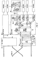
- Figs. 1 and 2 illustrate, in block diagram form, a communication system utilizing the switching architecture of the present invention;
- Fig. 2A functionally illustrates a switch node within the network architecture;
- Fig. 3 illustrates the contents of a call setup packet which is routed from an originating customer terminal to a destination customer terminal through the switching system;
- Fig. 4 illustrates the contents of the call reply packet transmitted from the destination customer terminal to the originating customer terminal in response to the receipt of the call setup packet;
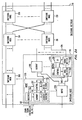
- Fig. 5 is a detailed block diagram of switching
network 116; - Fig. 6 illustrates a switch packet which is used to route the call setup packet of Fig. 3 from trunk controller 130 to
central processor 115 via switchingnetwork 116 andtrunk controller 129; - Figs. 7 through 9 illustrate the contents of the switch packet used to transmit the call reply packet of Fig. 4 through
switching network 116 as the packet progresses through the different stages of switchingnetwork 116 fromtrunk controller 131 to trunk controller 130; - Fig. 10 is a detailed block diagram of switching node 500-15 of switching
network 116; - Fig. 11 is a detailed block diagram of
input control 1000 of switching node 500-15; - Fig. 12 is a detailed block diagram of
address rotation circuit 1106 ofinput control 1000; - Fig. 13 is a detailed block diagram of
output control 1007 of switching node 500-15; - Fig. 14 illustrates, in block diagram form,
trunk controller 131; - Fig. 15 illustrates the logical organization of
memory 1401 oftrunk controller 131; - Figs. 16 through 26 are detailed block diagrams of subsystems which comprise
receiver 1402 oftrunk controller 131; - Fig. 27 is a detailed block diagram of
address control 1404 oftrunk controller 131; - Fig. 28 illustrates the logical operation of
address control 1404 in relationship tomemory 1401; - Fig. 29 is a detailed block diagram of the implementation of pointers as used in receive
interface 2701 ofaddress control 1404; - Fig. 30 is a detailed block diagram of receive
interface 2701; - Fig. 31 is a detailed block diagram of
switch interface 1418 oftrunk controller 131; - Figs. 32 through 40 are detailed block diagrams of subsystems which comprise
input circuit 1406 oftrunk controller 131; - Fig. 41 is a block diagram of
output circuit 1405 oftrunk controller 131; - Figs. 42 through 44 illustrate packet transformations performed by the subsystems of
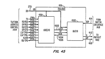
output circuit 1405 oftrunk controller 131 on packets read frommemory 1401 oftrunk controller 131; - Figs. 45 through 49 are detailed block diagrams of subsystems which comprise
output circuit 1405 oftrunk controller 131; - Figs. 50 through 53 are detailed block diagrams of subsystems which comprise
transmitter 1403 oftrunk controller 131; Fig. 54 is a timing diagram; and - Fig. 55 shows the manner in which certain of the figures should be arranged to show the specific illustrative embodiment of the invention.
- The drawing shows in Figs. 1 and 2 the heavy line block of a switching network for emphasis of the principal building block of the present invention. The details of that network are set forth on Figs. 10 through 13 and a functional illustration of the network is shown in Fig. 2A.
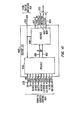
- Figs. 1 and 2 show an illustrative packet switching system having a plurality of
local offices customers customer 100resident interface 127 tocustomer 110resident interface 155 has the necessary self-routing information inserted into it by each trunk controller in its route through the packet switching system. Once the routing of the packet through the switching system has been described, the procedure used to compile the routing information is then described; and then, the method used to store this information in each trunk controller in the route is described. Finally, a detailed description of each block of Fig. 1 and 2 is given. - As shown in Fig. 1,
local office 102 comprises aswitching network 116 which terminates a plurality of trunk controllers and which cooperates withcentral processor 115 via a centralprocessor trunk controller 129 which is also connected to the switching network. Each trunk controller is tied into the network by unilateral transmission media.Trunk controller 131, for example, receives information from switchingnetwork 116 viaconductor 132 and transmits information to switchingnetwork 116 viaconductor 133. - On the customer side of
local office 102, the local office is connected to customers via concentrators which are interconnected to the switching network via trunk controllers. A concentrator has an internal switching architecture similar to that of switchingnetwork 116 which is described in greater detail later and has a self-contained trunk controller which interfaces the concentrator to the attached trunk. The concentrator's trunk controller is similar totrunk controller 131 which is described in greater detail later. Each concentrator has connected to it a microprocessor which is used in conjunction with the attached access line controller to perform the initial call setup sequences and to provide call supervision as a supplement to the inherent selfrouting characteristics of the packets being transmitted through the packet switching system. The customer units are connected to the concentrators by the access line controllers. Each access line controller stores logical address and control information which is stored in the access line controller by the controlling microprocessor. This logical address information is used to control the first portion of the route taken by the packets transmitted through the attached switching network via the interconnecting trunk controller. Each access line controller is connected to a resident interface contained within each customer unit via standard bilateral transmission media. Packets are transmitted between the access line controllers and the resident interfaces using standard packet protocols which define three virtual channels for communication between the resident interface and the access line controller. - Each trunk controller comprises a memory containing a translation table for converting the logical addresses into switch addresses which are used by the switching network to route the packets to the destination trunk controller.
Switching network 116 is interconnected to toll offices such as 104 by high speed trunks with each trunk being terminated on both ends by a trunk controller. The subject matter of Fig. 1 is substantially duplicated in Fig. 2. - Turning now to Fig. 2A, a functional representation of switching
network 116, is shown comprising three stages of switching nodes.Switching node 200 through 201comprise stage 1, switchingnodes 210 through 211 comprise the second stage, and switchingnodes 220 through 221 comprise the third stage. More detail with respect to the modular interconnection of the various switching nodes is given in the discussion of Fig. 5. Each switching node modularly comprises four input control circuits and four output control circuits as illustrated by switchingnode 201. The other switching nodes are identical in design to switchingnode 201.Switching node 201 has fourinput control circuits 230 through 233 and fouroutput control circuits 240 through 243. Each input control circuit has one output cable connected to each of the output control circuits. The output cables carry both data and control signals between the input and output control circuits. The details of a switching node are given in the discussion of Fig. 10. The composition of an input control circuit is shown by the block diagram ofinput control 230, and further details of an input control circuit are given in the discussion with respect to Figs. 11 and 12. Similarly, the composition of an output control circuit is shown byoutput control control 243 and a more in depth discussion is given with respect to Fig. 13. - As a packet is initially received by
input control 230, the packet is variably buffered inmemory 251 viareceiver 250 until transmission can commence to an output control circuit designated by the address in the packet, such asoutput control 243. Assuming the address designatedoutput control 243, the retransmission starts as soon as switchingnode 211, can accept the packet; hence, it is not necessary to completely buffer a packet before retransmitting it. This variable buffering greatly reduces the time delay for switching packets throughnetwork 116 and is facilitated by the exchange of intranode signaling between the input and output control circuits within a node and by the internode signaling which takes place between the output control circuit of one node and the input control circuit of the designated switching node. The intranode signaling involves the utilization of request and grant signals between the input control circuits and the output control circuits after the input control circuit initially receives the start of the packet. The internode signaling involves the setting of the idle/busy flip-flop, such as flip-flop 261, in the output control circuit to the idle state by the connected downstream switching node when the latter is capable of receiving another packet. The downstream node sets the idle/busy flip-flop to the idle state by transmitting a link open, or packet communication available, signal to the output control circuit. In addition, the utilization of an address rotation circuit within the input control circuit properly to reposition the address bits before transmission to the next sequential node greatly increases the switching speed. - Considering Fig. 2A now in greater detail,
input control 230 is responsive to the start of a packet fromtrunk controller 131 to store the first portion of the packet intomemory 251 and to examine the address associated with the packet to determine the output control circuit designated thereby. Assuming thatoutput control 243 is so designated,control 252 requests permission to immediately commence transmission frommemory 251 tooutput control 243 by transmission of a request signal via cable 280. If the input control circuit of switchingnode 211 to whichoutput control 243 is connected vialink 281 is capable of accepting a packet, the idle/busy flip-flop 261 is setto the idle state. Upon receipt of the request signal frominput control 230,output control 243 transmits back a grant signal via cable 280 and properly conditiondata selector 263 to accept data from cable 280 if flip-flop 261 is set to the idle state. Upon receiving the grant signal,control 252 immediately causesmemory 251 to commence transmission tooutput control 243 viaaddress rotation circuit 253 andmultiplexer 254.Control 252 properly conditions multiplexer 254 to properly selectoutput control 243 for transmission. After the packet has been transmitted,output control 243 sets flip-flop 261 to the busy state. - The function of
address rotation circuit 253 is to rotate all address bits such that the two most significant bits of the address are always presented to the next succeeding switch node. This is necessary for the modularity of all packet switch node operations and for speed of packet switching since the input control circuits always base their selection on the two most significant bits of the address and do not have to delay their switch actions which would otherwise occur without the rotation. When switchingnode 211 receives the packet fromoutput control 243, the address is properly aligned so that the selection is immediately made based on that address. - When switches
node 211 is capable of accepting another packet, it sets flip-flop 261 to the idle state indicating that another packet can be transmitted to switchingnode 211 by transmission of the link open signal vialink 281. - Turning now from the network functions and structure, the procedure for obtaining and storing self-routing information in address memories of the appropriate address line controllers and trunk controllers is described. The information is obtained by a call setup packet being transmitted from the appropriate access line controller connected to the originating customer unit through the various microprocessors and central processors which are associated with the different concentrators and local and toll offices which form the route through which the call setup packet must transverse in order to reach the destination customer unit. As the call setup packet progresses along this route, each processing entity inserts a new logical address into the packet and stores the necessary logical and switch address information in the appropriate access line controller or trunk controllers. Once the call setup packet is received at the microprocessor attached to the concentrator to which the destination customer unit is connected via an access line controller, the receiving microprocessor transmits the appropriate logical and switch address information to the connected access line controller which stores it in its address memory; and the receiving microprocessor assembles and transmits a call reply packet which indicates that the call has been properly set up. After the call reply packet is received by the orginating customer access line controller, all the necessary routing information is set up in the access line controllers and trunk controllers forming the packet route so that packets can be directly routed through the switching networks without the packets having to be handled by the associated processing entities.
- The utilization of the call setup packet is now illustrated in greater detail by describing the establishment of a telephone call between
customers Customer 100 callscustomer 110 by dialing thecustomer 110 telephone number.Resident interface 127 collects the dialed digits in the conventional manner. Afterresident interface 127 has collected the dialed digits, it transmits the dialed digits in a packet via line 122 to access line controller 112a. In response to the packet received fromresident interface 127, access line controller 112a assembles and transmits the packet shown in Fig. 3 to microprocessor 111 viaconcentrator 112. The packet identifier field identifies this packet as a signaling packet and a "1" in the most significant byte of data field indicate that the packet is a call setup packet. The remainder of the data field contains the dialed telephone number. - Upon receipt of the packet of Fig. 3, microprocessor 111 examines the dialed telephone number and determines that a connection is required through switching
network 116. First, microprocessor 111 transmits to access line controller a new logical address to be used in subsequent packets and the switchaddress defining concentrator 112's trunk controller which connectstrunk 117 toconcentrator 112. This switch address is used byconcentrator 112 to route subsequent packets totrunk 117. Next, microprocessor 111 stores inconcentrator 112's trunk controller the switch address identifying access line controller 112a and information defining the virtual channel to be used by access line controller 112a in communicating withresident interface 127. Finally, microprocessor 111 assembles a packet similar to the one shown in Fig. 3, but having the logical address in the logical address field which had been stored in the address memory of access line controller 112a. This new packet is then transmitted tocentral processor 115 viaconcentrator 112,trunk 117, trunk controller 130, switchingnetwork 116, andtrunk controller 129. - Upon receipt of the packet from microprocessor 111,
processor 115 determines from the dialed telephone number by performing a table look-up operation that the call must be sent through tooffice 104.Processor 115 first transmits the logical address contained in the received packet and the switch address identifying trunk controller 130 totrunk controller 131.Trunk controller 131 stores this address information in an internal memory and uses this information to perform the necessary logical to switch address translation on subsequent packets associated with the call being set up.Processor 115 then transmits to trunk controller 130 a new logical address and the switch address identifyingtrunk controller 131. This address information is used to perform the necessary logical to switch address translation for routing packets from trunk controller 130 totrunk controller 131 associated with the call being set up throughswitching network 116. The last operation performed byprocessor 115 is to transmit a call setup packet similar to that shown in Fig. 3 tocentral processor 113 via switchingnetwork 116,trunk controller 131,trunk 118,trunk controller 140 andswitching network 146. The packet transmitted toprocessor 113 has in the logical address field the logical address information identical to that previously stored in trunk controller 130. - Upon receipt of the packet from
trunk 118,processor 113 performs operations in response to this packet similar to those performed byprocessor 115 as previously described with respect to the call setup packet.Processor 113 then transmits a call setup packet tocentral processor 123 via switchingnetwork 146,trunk controller 142,trunk 119trunk controller 147, and switchingnetwork 148.Processor 123 performs similar operations to those performed byprocessor 113 and transmits a new call setup packet tocentral processor 114 via switchingnetwork 148,trunk controller 149,trunk 120,trunk controller 150, and switchingnetwork 151. Upon receipt of the call setup packet fromprocessor 123,central processor 114 stores the logical address information of this packet and the switch address designatingtrunk controller 150 intrunk controller 141.Central processor 114 then transmits a new logical address and the switch address designatingtrunk controller 141 totrunk controller 150, which stores this information. After storing the necessary information intrunk controllers processor 114 assembles a new call setup packet having the logical address which had previously been stored intrunk controller 150 in the logical address field and transmits this call setup packet tomicroprocessor 125 via switchingnetwork 151,trunk controller 141,trunk 124, andconcentrator 126. - Upon receipt of the call setup packet from
processor 114,microprocessor 125 reads the logical address information contained in the logical address field and stores the logical address inaddress memory 152 ofaccess line controller 126a.Microprocessor 125 then transmits a call reply packet as illustrated in Fig. 4 to microprocessor 111 via the previously defined route through the packet switching systems of Figs. 1 and 2. The logical address field of the packet of Fig. 4 contains the logical address whichmicroprocessor 125 received in the call setup packet fromprocessor 114.Trunk controller 141 is responsive to the receipt of the packet of Fig. 4 to translate the contents of the logical address field using the previously stored logical address to switch address translation information and to insert the previously stored logical address into the call reply packet. The switch address which results from this translation bytrunk controller 141 designatestrunk controller 150. This switch address is used by switchingnetwork 151 to route the call reply packet totrunk controller 150.Trunk controller 150 is responsive to receipt of the call reply packet to transmit this packet totrunk controller 149 viatrunk 120. The call reply packet is similarly routed through the various trunk controllers until it is received by microprocessor 111. Once the call reply packet is received by microprocessor 111, all the necessary information for routing calls through the various switching networks is stored within the trunk controllers and access line controllers in the route. -
Switching network 116 oflocal office 102 is shown in greater detail in Fig. 5. All connections to switchingnetwork 116 are made through the trunk controllers shown on Fig. 1. The trunk controllers receive information at a 1.54 Mb/s rate and transmit this information into the network at an 8 Mb/s rate. Each trunk is capable of buffering five packets of information from the attached trunk. The buffering of packets at the input from the trunks is necessary because the packets may have to be delayed before they can be transmitted through the network. Buffering is also needed by the trunk controllers for information being received from the network before it can be retransmitted on the attached trunk. Each trunk controller is capable of buffering up to 40 packets of information from the network before commencing retransmission out on the trunk. Each trunk controller has one input connection and one output connection to switchingnetwork 116. For example, trunk control 130 transmits information to switchingnetwork 116 viaconductor 134 and receives data from switchingnetwork 116 viaconductor 135 as shown in Fig. 5. - The network itself comprises three stages of switching nodes. The first stage comprises nodes 500-0 through 500-15, the second stage comprises switching nodes 501-0 through 501-15, and the third stage comprises switching node 502-0 through 502-15. Transmission through the network is from left to right. Each switching node is a packet switch. Each packet switch has four inputs and is capable of buffering one packet on each input. The packets received on any input are transmittable on any of the four output terminals of the packet switch. After receipt of a packet on an input terminal, the address contained in that packet is used to determine which output terminal should be used to retransmit the packet. Only the two most significant bits of the address are used to designate the output terminal for a particular switching node. For example, switching node 500-12 retransmits the packet on
line 505 if the most significant bits are equal to zero, online 506 if the most significant bits are equal to one, online 507 if the most significant bits are equal to two, and online 508, if the most significant bits are equal to three. - Each note properly rearranges the address bits so that the receiving switching node in the next stage has the correct bits in the most significant bit positions in order to determine which output terminal should be used to retransmit the packet at that stage.
- The operation of switching
network 116 as shown in Fig. 5 can be better understood by considering the example of the switching of the packet shown in Fig. 3 through this network tocentral processor 115. The packet shown in Fig. 3 is transmitted by microprocessor 111 viatrunk 117 to switchingnetwork 116. Upon receipt of the packet shown in Fig. 3, trunk controller 130 forms a new packet which is illustrated in Fig. 6. - The new packet is formed by taking the original packet received from
trunk 117, removing the flags and stuffed bits, and then adding the new fields of start bit, packet length, destination trunk controller, source trunk controller, control, arrival time, and a new CRC field. Trunk controller 130 responds to the packet identifier containing a "0" by inserting a "0" into the destination trunk controller field. This is the trunk number fortrunk controller 129 to whichcentral processor 115 is connected. Trunk controller 130 inserts its own output connection number on switching network 116 (in this example 48) into the source trunk controller field. The start bit defines the start of the network packet and the packet length defines the length of the network packet. Trunk controller 130 inserts into the arrival time field the relative time of day. Once the packet of Fig. 6 has been formed and theinput 513 of node 500-12 is idle, trunk controller 130 transmits this packet to node 500-12. - Node 500-12 examines the most significant bits of the address field and selects
output 505 since these bits are zero. Before transmitting thie packet to node 501-12 viaoutput terminal 505, node 500-12 rotates the address field two bits to the left; this results in the two most significant bits becoming the least significant bits, and the two middle bits of the address field shown in Fig. 6 becoming the two most significant bits. - Node 501-12 examines the address field upon receiving it and selects
output 512 since the most significant bits are zero. Node 501-12 also rotates the address field two bits to the left. Node 501-12 transmits the packet to node 502-0 via theoutput terminal 512. Upon receipt of the packet, node 502-0 examines the address field and selectsoutput terminal 514 since the two most significant bits of the address are zero. Upon receiving the packet,trunk controller 129 strips off the start bit, network address field, and network packet length, and transmits tocentral processor 115 the packet identifier, logical address, time stamp, and data fields plus a recalculated CRC field. - A second example will be used to help illustrate the operation of switching
network 116 as shown in Fig. 5. This will be done by following the transmission of the packet shown in Fig. 4 throughswitching network 116 fromtrunk 118 totrunk 117. Upon receipt of the packet shown in Fig. 4,trunk controller 131 forms the packet shown in Fig. 7. After forming this packet,trunk controller 131 transmits this packet to switching node 500-15 viainput terminal 515. Switching node 500-15 examines the two most significant bits of the network address field (in this example a binary three), and selects link 516 to transmit the packet shown in Fig. 7. Before switching node 500-15 starts to transmit the packet vialink 516, switching node 500-15 performs a left rotate operation on the network address field, and the result is the packet shown in Fig. 8. Upon receiving the packet from switching node 500-15, switching node 501-15 examines the two most significant bits of the network address field as shown in Fig. 8 and selectsoutput 517 to transmit the packet out. Before transmitting the packet, switching node 501-15 performs a left rotate operation on the packet, resulting in the packet shown in Fig. 9. Upon receiving the packet of Fig. 9, switching node 502-12 responds to the network address field by transmitting the packet to trunk controller 130 viaconductor 135. Switching node 502-12 also performs the left rotate operation on the network address field. The packet that is transmitted to trunk controller 130 viaconductor 135 is identical to the packet shown in Fig. 9 with the network address field rotated. Trunk controller 130 forms a new packet which is identical to that shown in Fig. 9 with the exception that the start bit, network packet length, destination trunk controller, source trunk controller, control, and arrival time fields have been eliminated, a new CRC field has been calculated and inserted, and the time stamp field has been updated. Trunk controller 130 then retransmits this new packet ontrunk 117. - It would be obvious to one skilled in the art to expand
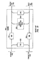
network 116 as shown in Fig. 5 to be capable of terminating more trunks by the addition of more switching nodes. In addition, it would be obvious to one skilled in the art to use such a switching network to correctly interconnect several pieces of digital equipment such as computers or terminals. The other switching networks and concentrators shown in Fig. 1 and 2 are similar in design to switchingnetwork 116. - Switching node 500-15 is illustrated in greater detail in Fig. 10. The other switching nodes are identical in design to switching node 500-15. The switching node consists of four input controls which can transmit information to any one of four output controls. The input controls 1000 through 1003 are connected to the output controls 1004 through 1007 via cables. For example,
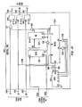
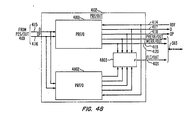
input control 1000 is connected tooutput control 1007 viacable 1008.Cable 1008 comprises threeconductors cable 1008. - When
input control 1000 has a packet to transmit tooutput control 1007, it transmits a request signal viaconductor 1010 tooutput control 1007.Input control 1000 continuously transmits this request signal until the entire packet has been transmitted tooutput control 1007. Whenoutput control 1007 is free to receive information frominput control 1000,output control 1007 transmits a grant signal viaconductor 1011 to inputcontrol 1000. Upon receipt of the grant signal,input control 1000 commences to transmit the packet tooutput control 1007 viaconductor 1009. - For example, the packet shown in Fig. 7 would be transmitted through switching node 500-15 as illustrated in Fig. 10 in the following manner. When
input control 1000 recognizes the start bit, it has already received not only the start bit but also the two most significant bits of the network address.Input control 1000 decodes the two most significant bits of the network address field and determines that the packet was to be transmitted tooutput control 1007 viacable 1008.Input control 1000 requests permission to start transmission viaconductor 1010; and whenoutput control 1007 returns the grant signal viaconductor 1011,input control 1000 starts the transmission of the packet tooutput control 1007 viacable 1008. Before transmitting the network address field,input control 1000 left rotates this address two bits so that the network address transmitted is that shown in Fig. 8. Upon receipt of the start bit of the packet,output control 1007 starts to retransmit this packet out onlink 516. -
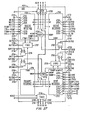
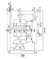
Input control 1000 of Fig. 10 is shown in greater detail in Fig. 11. Input circuit 1110 receives the information frominput terminal 515 and transmits to trunk controller 130 of Fig. 11 the link open signal viainput terminal 515 under control ofcontroller 1104. The function of the link open signal will be explained in a later section describingoutput control 1007.Input shift register 1100 is used to detect the start bit, which indicates the beginning of a packet. In addition,input shift register 1100 is used to extract the network packet length field, which is saved inlength register 1102, and to extract the two most significant bits of the network address field, which are saved inaddress register 1101. Thebuffer shift register 1103 is capable of buffering one complete packet.Buffer shift register 1103 provides an output after each 64 bits of storage. These outputs can be selected bydata selector 1105 under control ofcontroller 1104 to bypass unused portions of thebuffer shifter register 1103. This bypassing is done when it is not necessary to buffer a whole packet before transmission of the packet can start to the output circuit and is done to speed up the transfer of a packet throughinput control 1000.Address rotation circuit 1106 performs the previously mentioned left rotate operation on the network address field before this address is transmitted with the remainder of the packet to the selected output control. Multiplexer 1107 under control ofcontroller 1104 selects which of thecables - The operation of
input control 1000 will now be further explained by using the previous example which dealt with the transmission of the packet shown in Fig. 7.Input shift register 1100 is continuously being clocked bysystem clock 161 via conductor 1111. As data is received viainput terminal 515, it is clocked throughinput shift register 1100. Once the start bit reachesbit position 10 ofinput shift register 1100,controller 1104 detects this bit and transmits a pulse onconductor 1113. This pulse causeslength register 1102 to store the network packet length field, and causesaddress register 1101 to store the two most significant bits of the network address field, which are contained inbit positions input shift register 1100. -
Controller 1104 transmits a request viaconductor 1010 tooutput control 1007 since the most significant address bits indicate that the packet is to be transmitted to this output control. While this request is being made, data is being shifted frominput shift register 1100 to buffershift register 1103 which has a number of output terminals. These output terminals are connected to different bit positions withinbuffer shift register 1103. Whencontroller 1104 receives a grant signal fromoutput control 1007 viaconductor 1011,controller 1104 calculates at which output ofbuffer shift register 1103 the start bit of the packet is approaching withinbuffer shift register 1103. This is done so that transmission of the packet tooutput control 1007 can start as soon as possible. On the basis of this calculation,controller 1104 controlsdata selector 1105 to select the designated output ofbuffer shift register 1103. The control information is transmitted todata selector 1105 viacable 1117.Data selector 1105 transmits the data from the selected output to addressrotation circuit 1106 viaconductor 1116. Before transmitting data,controller 1104 resetsaddress rotation circuit 1106 by transmitting the start of packet signal viaconductor 1119. The controller 1104then uses the packet length information stored inlength register 1102, which it reads viacable 1120, to determine when the end of the packet has entered the input shift register. When this occurs and transmission has started fromshift register 1103,controller 1104 transmits the link open signal viaconductor 1115. This signal is retransmitted viatri-state driver 1109 andinput terminal 515 to input port 503-60. The link open signal indicates thatinput control 1000 is now ready to receive another packet. This function is explained in the section dealing with the output control circuit. -
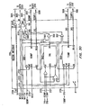
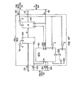
Address rotation circuit 1106 is illustrated in greater detail in Fig. 12. The purpose ofcircuit 1106 is to rotate the address field to the left two bits so that the two most significant bits become the least significant bits. The rotation is necessary because each input control decodes only the two most significant bits.Shift registers data selector 1202 is used to select either the output ofshift register 1200 orshift register 1203, andcontrol circuit 1209 controls the operation of the address rotation circuit. Whencontrol circuit 1209 receives the start of packet signal fromcontroller 1104 viaconductor 1119, it transmits a clock signal to shiftregister 1200 viaconductor 1207, and toshift register 1203 viaconductor 1205. This clock signal is derived from the signal received fromsystem clock 161 viaconductor 1210.Control circuit 1209conditions data selector 1202 viaconductor 1208 to selectshift register 1203's output to be transmitted onconductor 1118.Control circuit 1209 then counts the number of bits that are being transmitted viaconductor 1118; when the two most significant bits of the network address field are contained withinshift register 1203,control circuit 1209 ceases to transmit the clock signal to shiftregister 1203 viaconductor 1205, andconditions data selector 1202 to select the output ofshift register 1200.Control circuit 1209 then waits until the remaining bits of the network address field have been transmitted viaconductor 1118. At this point in time,control circuit 1209 commences to send clock signals to shiftregister 1203, andconditions data selector 1202 to select the output ofshift register 1203. This operation results in the most significant bits of the network address field being rotated. -
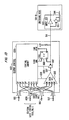
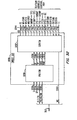
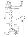
Output control 1007 is shown in greater detail in Fig. 13.Control circuit 1300 responds to requests frominput controls 1000 through 1003, which are transmitted viacables flop 1301 is set,control circuit 1300 responds to the request by transmitting a grant signal back to the requesting input control via one of the above mentioned cables. After acknowledging the request,control circuit 1300conditions data selector 1303 to select the data conductor from theappropriate cable Control circuit 1300 transmits the appropriate control information todata selector 1303 viacable 1308.Data selector 1303 transfers the data information received on the selected input terminal toconductor 1307.Tri-state device 1302 takes the information onconductor 1307 and transmits this data vialink 516 to inputcircuit 1305, which is part of switching node 501-15.Control circuit 1300 controls the output oftri-state device 1302 viaconductor 1309. - The operation of
output control 1007 as shown in Fig. 13 will be explained in greater detail by considering the previous example ofinput control 1000 transmitting a packet of data tooutput control 1007 viacable 1008. Wheninput control 1000 transmits the request signal viaconductor 1010,control circuit 1300 transmits the grant signal to inputcontrol 1000 viaconductor 1011 if thelink 516 is not being used by one of the other input control circuits and the output of flip-flop 1301 is set. Assuming that flip-flop 1301 was set,control circuit 1300 transmits the grant signal to inputcontrol 1000 andconditions data selector 1303 viacable 1308 to select the data being transmitted onconductor 1009 and retransmit this data onconductor 1307. In addition,control circuit 1300 enables thetri-state device 1302 to transfer the information onconductor 1307 to link 516. - After
input control 1000 has transmitted the entire packet, it removes the request signal fromconductor 1010. Once the request signal is removed fromconductor 1010,control circuit 1300 sends a reset signal to flip-flop 1301 viaconductor 1310 and stops transmitting signals viacable 1308 andconductor 1309. Once the input control of the switching node 501-15 is capable of accepting another packet, it transmits the open link signal viaconductor 1306, tri-state device 1311, and link 516. The open link signal sets flip-flop 1301 via the S input. Once flip-flop 1301 is set,control circuit 1300 can once again respond to request signals from the input controls. -
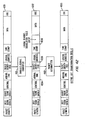
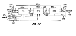
Trunk controller 131 is shown in greater detail in Fig. 14. The other trunk controllers are similar totrunk controller 131.Trunk controller 131 receives packets fromtrunk 118 viareceiver 1402, and transmits packets totrunk 118 viatransmitter 1403.Trunk 118 is illustratively a telephone digital transmission facility with a data transmission rate of 1.544 Nb/s as described in Boyle, Colton, Dammann, Karafin, and Mann, "Transmission/Switching Interfaces and Toll Terminal Equipment", 56 The Bell System Technical Journal 1057, 1058 (1977).Receiver 1402 andtransmitter 1403 are interfaced to the DSX-1 unit shown in Fig. 1 on page 1058 of the cited article.Trunk controller 131 transmits packets to switchingnetwork 116 viaoutput circuit 1405, and receives packets from switchingnetwork 116 viainput circuit 1406.Switch interface 1418 interfaces the input and output circuits to the switch network. Packets are transferred in and out of four circular buffers inmemory 1401 viaaddress control 1404.Address control 1404 contains pointers to the circular buffers that allowinput circuit 1406,output circuit 1405,transmitter 1403, andreceiver 1402 to read and writememory 1401. - Consider an example where normal data packets are transferred from
trunk 118 to switchingnetwork 116. Incoming packets, similar to those shown in Fig. 3, are received byreceiver 1402 in a serial fashion at a 1.544 Mb/s rate.Receiver 1402 adds the arrival time to the packet, and transforms the serial information into a byte. Once it has assembled a byte, it transmits a write request, viacontrol bus 1408, to addresscontrol 1404.Receiver 1402 then writes the byte intomemory 1401 viadata bus 1407 andaddress control 1404. The location inmemory 1401 that the byte is written into is designated by the address pointers associated withreceiver 1402. This process continues untilreceiver 1402 has transferred an entire packet intomemory 1401. Afterreceiver 1402 has transmitted an entire packet, it transmits an end of packet signal, viacontrol bus 1408, to addresscontrol 1404.Address control 1404 then transmits a packet available signal, viacontrol bus 1412, tooutput circuit 1405. This packet available signal is transmitted as long as there is a complete packet inmemory 1401. -
Output circuit 1405 reads the packet stored inmemory 1401 by making sequential read requests to addresscontrol 1404 viacontrol bus 1412.Address control 1404 maintains a pointer then determines which word inmemory 1401 is associated with the packet to be transmitted into the network viaoutput circuit 1405.Output circuit 1405 access and transmits packets at an 8 mb/s rate. In order to transmit packets to switchingnetwork 116,output circuit 1405 forms packets similar to those shown in Fig. 6. It does this by using the logical address field from the original packet to address the logical translation table, and calculating the packet length field. In addition,output circuit 1405 calculates a new CRC field, updates the control field, and adds a start bit. These operations are done in a serial fashion; however, an entire packet does not need to be buffered. - Consider another example where packets are transferred from switching
network 116 totrunk 118. Packets from switchingnetwork 116 are received byinput circuit 1406 viaswitch interface 1418.Input circuit 1406 forms this data into bytes. It then sends a write request viacontrol bus 1414, and sends the packets viadata bus 1413 to addresscontrol 1404.Address control 1404 writes the information intomemory 1401, viamemory address bus 1417,memory data bus 1415, andmemory control bus 1416. When an active packet has been stored inmemory 1401,input circuit 1406 transmits an end of packet signal to addresscontrol 1404 viacontrol bus 1414.Address control 1404 then transmits a packet available signal totransmitter 1403 viacontrol bus 1410.Transmitter 1403 makes a read request to addresscontrol 1404, and receives the packets viadata bus 1409.Transmitter 1403 transforms the packets into packets similar to those in Fig. 4, and transmits them totrunk 118 at a 1.544 Mb/s rate.Transmitter 1403 also performs error checking, and recalculates the CRC field. In addition,transmitter 1403 updates the time stamp field of the packet. It does this by subtracting the arrival time from the present time, and adding this difference to the time stamp field. -
Trunk controller 131 handles a variety of packets that are used for various purposes. These packets can be divided into the following general categories: normal data packets, trunk and switch test packets, maintenance read and write packets, and memory read and write packets. The types of packets are distinguished by different values in the packet identifier or control fields. Normal data packets carry data and signaling information between the trunk and switching network. These are the most common packets. Trunk test packets are used to test a trunk, including the two trunk controllers, and the actual trunk facility. This is done as follows. The test packet is formed by the associated central processor, and sent to the first trunk controller via the switching network. The first trunk controller performs a check on the CRC field of the packet to determine if any errors occurred during the transmission. If an error is found, the first trunk controller aborts the test packet; if no errors are found, the first trunk controller sends the test packet to the second trunk controller via the trunk facility. When the second trunk controller receives the test packet, it performs the same CRC check and, if no errors are found, loops the packet back to the first trunk controller, which then sends the packet back to the central processor, via the switching network. The central processor detects that a transmission error has occurred by noting that the test packet is not looped back after a period of time has elapsed. Switch test packets are used to test a path within the switching network. A switch test packet as sent by the central processor to a trunk controller through the switching network. The trunk controller relays the packet to a second trunk controller (specified in the packet), which then returns the packet to the central processor. Maintenance packets are used to send maintenance information, such as error statistics, between a trunk controller and its associated central processor. In a maintenance read operation, the central processor sends a maintenance read packet to the trunk controller. The trunk controller reads the information and writes it into the packet; it then returns the packet to the central processor. In a maintenance write operation, the central processor sends a maintenance write packet to the trunk controller. The trunk controller writes the information from the packet into the maintenance register, and then reads the same information out of the maintenance register. The information read out is placed in the maintenance write packet and sent back to the central processor. Memory packets allow the central processor to read and write information from specified memory locations. These packets work similarly to maintenance packets, with the exception that memory locations, and not the maintenance register, are read and written. - Fig. 15 illustrates the four packet buffers, and logical channel translation table contained in
memory 1401. Packets arriving fromreceiver 1402 are written into either receivebuffer 1501 ortrunk test buffer 1502.Trunk test buffer 1502 is reserved for test packets that are to be looped back over the trunk. All other arriving packets are sent to receivebuffer 1501. Packets arriving frominput circuit 1406 are written into either transmitbuffer 1503 orswitch test buffer 1504. Transmitbuffer 1503 is for packets that are to be transmitted on the trunk viatransmitter 1403.Switch test buffer 1504 is for switch test packets, and for memory read and write packets. Logical translation table 1505 contains the logical to physical address translation information received from the central processor via memory write packets. - The reading and writing of the circular buffers in
memory 1401 is controlled by read and write pointers, located inaddress control 1404. These read and write pointers point to the specific memory locations within the various buffers. Read or write pointers are provided forreceiver 1402,transmitter 1403,input circuit 1406 andoutput circuit 1405. These pointers are used to read or write the various circular buffers, depending on the circuit. The structure is as follows: Receive circuit-receive buffer and trunk test buffer write pointers; output circuit-receive buffer and switch test buffer read pointers; input circuit-transmit buffer and switch test buffer write pointers; transmit circuit-transmit buffer and trunk test buffer read pointers. - In addition to the various read and write pointers,
address control 1404 also contains temporary pointers.Receiver 1402 has access to one temporary pointer, which is used to save the value of the write pointer. At the beginning of each packet write operation, the temporary pointer is set to the same address as the write pointer. If an error is discovered while the packet is being written, the write pointer is set back to the address of the temporary pointer. In this way, the packet containing an error is overwritten, effectively discarding it.Input circuit 1406 has access to two temporary pointers. One is used to save the value of the write pointer. The other temporary pointer is used during memory write operations, and will be discussed later.Output circuit 1405 has access to one temporary pointer, which is used during memory read operations. - The following description shows the packet flow of an ordinary data packet from the trunk to the switch network.
Receiver 1402 receives trunk packets, and pads the trunk packets with zeroes, in order to provide space in the packet to transform the trunk packets into switch packets. Oncereceiver 1402 has done this, it makes a write request to addresscontrol 1404, in order to write the packet into receivebuffer 1501 inmemory 1401.Address control 1404 receives the write request and makes the receive buffer write pointer available.Receiver 1402 then writes the packet into receivebuffer 1501 at the address specified by the write pointer.Address control 1404 then sends a packet available signal tooutput circuit 1405, causingoutput circuit 1405 to send a read request to addresscontrol 1404.Address control 1404 makes the receive buffer read pointer available, allowingoutput circuit 1405 to read receivebuffer 1501 at the address specified by the read pointer.Output circuit 1405 reads the packet, modifies the necessary fields to convert the trunk packet into a switch packet, performs the necessary logical to physical address translation, and sends the packet to the switching network. The logical to physical address translation involves reading the logical translation table inmemory 1401, and updating the required packet fields. - The packet flow of an ordinary data packet from the switch network to the trunk is as follows. The packet is received from the switching network via
switch interface 1418, and is sent to inputcircuit 1406.Input circuit 1406 makes a write request to addresscontrol 1404, in order to write the packet into transmitbuffer 1503 inmemory 1401.Address control 1404 receives the write request and makes the transmit buffer write pointer available.Input circuit 1406 then writes the packet into transmitbuffer 1503, at the address specified by the write pointer.Address control 1404 then sends a packet available signal totransmitter 1403, causingtransmitter 1403 to send a read request to addresscontrol 1404.Address control 1404 makes the transmit buffer read pointer available, allowingtransmitter 1403 to read transmitbuffer 1503 at the address specified by the read pointer.Transmitter 1403 makes a read request to addresscontroller 1404, in order to read the packet from transmitbuffer 1503. Oncetransmitter 1403 has read the packet, it removes the header information from the packet, which transforms the packet into a trunk packet.Transmitter 1403 then transmits the packet on the attached trunk. - Trunk test packets are received by
receiver 1402 from the trunk. They are written intotrunk test buffer 1502 inmemory 1401, using the trunk test buffer write pointer inaddress control 1404. This operation is similar to the operation of the receive buffer write pointer.Transmitter 1403 then makes a read request to addresscontrol 1404, in order to readtrunk test buffer 1502, using the trunk test buffer read pointer. Oncetransmitter 1403 has read the test packet, it transmits it back to the trunk. Switch test packets are processed in a similar manner. They are received byinput circuit 1406, which writes then intoswitch test buffer 1504 inmemory 1401, using the switch test buffer write pointer.Output circuit 1405 then readsswitch test buffer 1504, using the switch test buffer read pointer inaddress control 1404. Once it has read the packet, it sends it to the specified trunk controller via the switch network. - Memory write packets are used to write information into
memory 1401. This information includes the logical to physical address translations, which are written into logical translation table 1505. Memory write packets are originated by the central processor, and are sent to inputcircuit 1406, which writes part of the packet intoswitch test buffer 1504, and part of the packet into logical translation table 1505, both located inmemory 1401. The portion of the memory write packet that is written intoswitch test buffer 1504 is written via the switch test buffer write pointer; the portion of the packet that is written into logical translation table 1505 is written via the second input circuit temporary pointer, both located inaddress control 1404.Output circuit 1405 then reads the information stored inswitch test buffer 1504, and reads the logical translation information. It then assembles these two portions of data into a packet that is identical to the original memory write packet, and transmits this packet back to the central processor. - Memory read packets are originated by the central processor, and are used to allow the central to read portions of
memory 1401. The incoming memory read packet contains the memory address, and the number of bytes to be read.Output circuit 1405 readsmemory 1401 at the address specified in the packet, and inserts the number of bytes specified into the memory read packet. It then returns the packet (containing the requested data) to the central processor. - Trunk and switch packets are further described with respect to the fields contained in each of these two packet types. The actual packet manipulation and conversion details are described later. Trunk packets carry data and maintenance information between the trunk equipment and the trunk controllers. The format of a typical trunk packet is shown in Fig. 3. An explanation of the fields is given in the following paragraphs.
- The flag field is a unique bit pattern (01111110) used to identify the beginning and end of a packet. The packet identifier (PID) field determines whether the packet is for signaling, testing, or the transmission of normal data. A "0" in this field indicates a signaling packet used for call set-up. As previously described, this packet is routed through all central processors along the path, in order to establish the path that all subsequent packets will take for the duration of the call.
- A PID field of "1" indicates a signaling packet that sends signaling information over a path that has already been established. This packet type is read only at the terminating central office.
- A PID field of "2" or "3" is a test packet, which is used to test a trunk in the network. The originating central processor sends a test packet to one of its trunk controllers, via the switching network. This packet is indicated by a PID field of "2". The packet is transmitted by the first trunk controller over the trunk to a second trunk controller. Since the PID field is a "2", the second trunk controller changes the field from a "2" to a "3" and loops the test packet back to the first trunk controller over the trunk. The first trunk controller receives the packet, and reads the PID field. Since the PID field is a "3", the first trunk controller returns the packet to the central processor.
- A PID field of "8" through "11" identifies the packet as one carrying normal data. The ascending order of numbers indicates levels of flow control. An "8" indicates no flow control. The numbers "9" through "11" indicate increasing levels of flow control. When flow control increases, the originating office sends the packets out with a greater amount of time in between. This is to prevent system overload due to increased traffic.
- A PID field of "12" indicates a datagram. This is a single packet that carries a complete message. A datagram is routed as follows. A datagram is created by the central processor associated with the terminal equipment sending the datagram. The datagram is then routed to each central processor in the network that the datagram passes through. Each central processor reads the logical address field of the datagram to determine the next central processor to which the datagram is sent. Once the datagram reaches the destination central processor, the destination central processor routes the datagram to the destination customer's terminal equipment. The address information is not retained because a path is not required to send additional packets.
- The logical address field is used to derive the address of the destination trunk controller. This is done by the current trunk controller using the logical address to index logical translation table 1505 contained in
memory 1401. Logical translation table 1505 contains the number of the next trunk controller and the new logical address. The current trunk controller inserts the new logical address into the packet's logical address field and then routes the packet. The time stamp field carries the accumulated time that it takes for the packet to travel through the switch system. This field is updated in conjunction with the arrival time field, which is inserted when the packet is first received from the trunk. When the destination trunk controller receives a packet, it calculates the difference between the arrival time and the present time, in order to update the time stamp field. The data field contains the actual data, or information, that the packet is to carry. In addition, this field carries certain high level protocol information. The cyclic redundancy code (CRC) field is used for error detection. This field is generated by the transmitting trunk controller, and tested by the destination trunk controller, in order to determine if the packet contains errors. - Switch packets carry data and maintenance information within the switching network. The format of a typical switch packet is shown in Fig. 6. A data type switch packet contains all the fields contained in a trunk packet, and in the same order. The one exception is the two flag fields, which are not contained in the switch packet. Also, the CRC field is recalculated and checked at several stages of the transformation process from trunk packets to switch packets. An explanation of the fields unique to switch packets is provided in the following paragraphs.
- The packet length field is the total length of the packet, in bytes. This field is computed by
receiver 1402. The destination trunk controller (DTC) and source trunk controller (STC) fields are used for packet routing. The DTC is the address of the destination trunk controller and is obtained from logical translation table 1505. The STC field is the address of the trunk controller that is presently handling the packet. - As given in the following Table 1, the control field, CNTL, defines the type of switch packet.

- Standard data packets carry the information contained in data type trunk packets (packet identifier of "8", "9", "10", or "11"), as well as signalling and datagram packets (packet identifier of "0", "1", or "12") through the switch network. These packets are transformed back to trunk packets by the next trunk controller in the network, and then transferred back to switch packets, as required, for transmission through subsequent switch networks. Maintenance information is transmitted through the system with maintenance write and maintenance read packets. These packets give the central processor the ability to read and write maintenance information into the trunk controller. This maintenance information includes error and control information. A maintenance write packet is generated by the central processor and is sent to the appropriate trunk controller. Once this packet arrives at the trunk controller, the trunk controller examines the control field, determines that it is a "2" (indicating α-maintenance write) .and writes the data portion of the packet into
maintenance register 3101 inswitch interface 1418. - When the trunk controller receives a switch packet with at "1" in the control field, it performs a maintenance read operation. The data in the maintenance register is read, and stored in the data portion of a packet. The packet is then transmitted to the originating central processor.
- Switch packets ar also used to read and write the memory portion of the trunk controller. In a memory write operation, the switch packet's control field is a "3".
Input circuit 1406 receives the packet from the central processor, writes the data portion into the requested location inmemory 1401, and writes the rest of the packet intoswitch test buffer 1504.Output circuit 1405 reads the data from the specified location inmemory 1401, and reads the remainder of the packet fromswitch test buffer 1504. It then assembles a new packet from these two segments, and transmits the new packet back tocentral processor 115 via switchingnetwork 116. - A test packet is a type of switch packet that can route test data through two trunk controllers, before routing the packet back to the central processor. When the test packet arrives at the first trunk controller, the control field is set-to "5". This indicates that the packet is to be routed to a second trunk controller before being returned to the central processor. Before leaving the first trunk controller,
output circuit 1405 changes the control field from a "5" to a "6", and then sends the packet to the second trunk controller. The address of the second trunk controller is specified in the data field. After the second trunk controller receives the test packet, it reads the control field. Since the field is a "6", the second trunk controller routes the packet directly to the central processor. - The main function of
receiver 1402 is to convert trunk packets, received from the trunk side of the network, into switch packets, which are then transmitted through the switching part of the network. The conversion consists of (1) removing the start and end flag fields, and (2) adding fields at the beginning of the packet. The transformation also requires that the CRC field be recalculated. The added fields are as follows. The first two added fields, destination trunk controller and source trunk controller are filled with zeroes. The actual source and destination trunk controller values are added byoutput circuit 1405 after it reads the packet from receivebuffer 1501. The next added field is the control field. The last added field is the arrival time field. This field is filled in with the actual time that the packet arrives atreceiver 1402, and is used by the destination trunk controller to update the time stamp field. - During packet conversion, the destination trunk controller, source trunk controller and control fields are initialized to zero. The arrival time field is initialized to the arrival time of the packet (expressed as a negative number). The packet identifier field is unchanged, with one exception: if the packet identifier field of the incoming packet is a "2", indicating a test packet, it is changed to a "3", indicating a trunk test packet that is returning. As already mentioned, the CRC field is updated; however, the updating process has this complication: the CRC field is computed as though the packet length field contained all zeros, and the actual length of the packet was contained in a separate field between the data and CRC fields. The reason for this is because the length of the packet is being computed as the packet comes in, and is not known until the entire packet is received.
-
Receiver 1402 is shown in greater detail in Fig. 16.Receiver 1402 comprises flag removal and bitunstuffing circuit 1601,packet reformatter 1602, and serial toparallel converter 1603. Flag removal and bitunstuffing circuit 1601 removes the 01111110 flag pattern at the beginning and end of the trunk packet. - Additionally, this circuit removes bits that were stuffed into the bit stream by
transmitter 1403. This process is explained later.Packet reformatter 1602 adds zeroes to the packet. These zeroes serve as place holders for the fields added during the packet transformation. In addition, this circuit fills in the arrival time of the packet, and updates the packet identifier field, as required. - The trunk packets are received by flag removal and bit
unstuffing circuit 1601 onconductor 1604. This circuit detects the start and end points of each packet by detecting the presence of the start and stop flags contained in the packet. Once the flags are detected, they are removed. In addition, this circuit performs bit unstuffing. Bit unstuffing is the removal of bits that were placed in the bit stream to ensure that the flag pattern does not occur at any place other than the start and end of the packet. - Flag removal and bit
unstuffing circuit 1601 sends the packets topacket reformatter 1602 viaconductor 1605. A signal is placed onconductor 1606 when the packet first arrives atpacket reformatter 1602. This signal remains as long as the packet is being processed. A similar signal is present onconductor 1609 during the time that the packet is being transferred frompacket reformatter 1602 to serial toparallel converter 1603. A "1" is placed onconductor 1607 during every clock pulse thatconductor 1605 contains data.Packet reformatter 1602 receives the trunk packet from 1601 and adds the appropriate fields to allow the forming of a switch packet. In addition, this circuit performs error detection, and modifies the PID field as required. - Error detection is done by checking the CRC field of each incoming packet. If an error is detected, 1602 transmits an error signal to 1603 via
conductor 1612, which causes the packet containing the error to be aborted.Packet reformatter 1602 also detects hardware errors. If a hardware error is found, it is indicated by a signal onconductor 1626. - The PID field modification performed by 1602 is with respect to trunk test packets. An incoming test packet has a PID of "2"; 1602 changes the field to a "3". Additionally, when a test packet is received, 1602 causes
conductor 1611 to go high. This causes serial toparallel converter 1603 to write the contents of the test packet intotrunk test buffer 1502.Packet reformatter 1602 is fully duplicated and thus is capable of doing fault detection of itself. - Flag removal and bit
unstuffing circuit 1601 is shown in greater detail in Fig. 17. This circuit does flag removal and bit unstuffing. Flag removal is performed as follows. A flag pattern of 01111110 is continuously sent overconductor 1604 whenever the trunk is idle. This 8-bit pattern is read intoregister 1701. At the same time that register 1701 is receiving the bit pattern,register 1702 is receiving a steady stream of "1's" at the same bit rate. After a complete 8-bit flag pattern is received,register 1702 is cleared via a "1" on the output of ANDgate 1706, which decodes the presence of the flag pattern. This prevents the "1's", which are being clocked intoregister 1702, from being sent out ofregister 1702. The "1's" coming out ofregister 1702 are routed to ANDgate 1714 andregister 1705. When "1's" are present, actual data is allowed to flow out ofregister 1701, andconductor 1607 is activated to signal this actual data. - After a flag pattern from an actual packet is clocked into
register 1701, the subsequent bits are actual packet contents rather than the flag pattern. After eight bits of actual data have been clocked intoregister 1701, ANDgate 1706 does notclear register 1702 because the AND gate is not detecting the flag pattern. This causesregister 1702 to send a continuous stream of "1's" to one input of ANDgate 1714. The other input of ANDgate 1714 is receiving the actual packet contents fromregister 1701. ANDgate 1714 is thus enabled by the "1's" coming out ofregister 1702. Because of the enable signal, the contents ofregister 1701 are allowed to be shifted intoregister 1703. Thus, the output of ANDgate 1714 is "1" only when the actual packet contents contain a "1". In this way, the packet contents minus the flags are shifted throughregister 1703 and are sent topacket reformatter 1602 via conductor 1710. - Bit unstuffing is required because whenever
transmitter 1403 detects five sequential "1's", it always stuffs a "0". This is so that the packet data never contains the flag pattern. These stuffed zeros are removed by flag removal and bitunstuffing circuit 1601 after the flags have been removed. Bit unstuffing is done as follows. The packet data coming out of ANDgate 1714 still contains the stuffed "0's". If a pattern of 11111 is clocked intoregister 1703, the next bit has to be a stuffed bit, which must be removed. This 11111 pattern causes the output ofNAND gate 1718 to go to "0" during the one bit time that the stuffed "0" is in the first position ofregister 1703. This "0" is shifted throughregister 1704 at the same time that the actual packet data is shifted throughregister 1703. When the "0" inregister 1704 reaches the input of ANDgate 1708,conductor 1606 goes to "0" for that one clock pulse that the stuffed "0" is present inregister 1703.Conductor 1606 is the bit present indicator, which is passed topacket reformatter 1602. Since the bit present signal is absent for any clock pulse that a stuffed "0" is contained inregister 1703, the stuffed "0" is removed. -
Packet reformatter 1602 is shown in greater detail in Fig. 18. This circuit performs the actual packet transformation. This circuit comprisesCRC circuits circuits comparator 1803. The CRC and packet reformat circuits are duplicated because during the reformatting process the CRC check cannot accurately detect errors within the circuit. The CRC circuits check the CRC field of the incoming packet and then remove it. The packet reformat circuits do the actual packet transformations and calculate the new CRC field.Comparator 1803 compares the reformatted packets frompacket reformat circuits conductor 1626. This FLTR signal is sent to switchinterface 1418, and then to the central processor, which then takes corrective action. -
Packet reformat circuit 1802 is shown in greater detail in Fig. 19. This circuit comprisespad circuit 1901, which adds blank fields to the incoming trunk packet to be used to form a switch packet by later circuits;arrival time circuit 1902, which calculates and fills in the packet arrival time;PID circuit 1903, which updates the PID field if required;length circuit 1904, which calculates and fills in the packet length; andCRC circuit 1905, which calculates the CRC field of the packet. -
Pad circuit 1901 is shown in greater detail in Fig. 20. Thiscircuit pads 56 zeroes at the beginning of the incoming packet, andpads 24 zeroes at the end of the packet. These zeroes serve as place holders for the fields that are added by the succeeding circuits.Pad circuit 1901 receives both psi and phi clock pulses fromsystem clock 161. The phi pulses are five times faster than the psi pulses, as shown in Fig. 54. The phi clock pulses are required to place the zeroes at the beginning of the packet. -
Pad circuit 1901 receives data, data present, and bit present signals onconductors gates 2006 through 2008, and are shifted intoregisters 2001 through 2003.Registers 2001 through 2003 shift data through at the psi clock rate through operated ANDgate 2010 andOR gate 2011. The first pulse onconductor 1815 activatescontrol 2004 viaconductor 2031. Whencontrol 2004 is activated, it activates counter 2005, andpad conductor 2027.Conductor 2027pads 56 zeroes to the beginning of the packet via ANDgate 2019 and flip-flop 2024.Counter 2005 counts the clock pulses and signals control 2004 via ANDgate 2030 to disableconductor 2027 after 56 pulses. The zeroes are padded at the phi clock rate; this allows the zeroes to be padded at the beginning of the packet before the actual packet data is shifted out ofregister 2001. When the data, data present and bit present signals are shifted out ofregisters 2001 through 2003 they are converted from 1.544 to 8 Mb/s, viagates flop 2015. When the last 16 bits of the packet are in register 2001 (signalled byconductor 2031 being disabled),control 2004 activatesconductor 2032. This causes the last 16 bits inregisters 2001 through 2003 to be shifted through at the phi clock rate, via operated ANDgate 2012 andOR gate 2011. Additionally, this signal disables ANDgates 2006 through 2008, viainverter 2009. The purpose of this is to prevent the next packet from being shifted into pad-circuit 1901 until the existing packet is shifted through. After the end of the packet is shifted out ofregister 2001,control 2004 enablesconductor 2027 for 24 clock pulses, causing 24 zeroes to be padded to the end of the packet. -
Arrival time circuit 1902 is shown in greater detail in Fig. 21. This circuit places the arrival time of the packet into the arrival time field. The arrival time is calculated as a negative, rather than positive, value. By running the clock in reverse, the arrival time can be added to the present time, avoiding the need to complement, as described later in the description oftransmitter 1403.Arrival time circuit 1902 comprisescounters shift register 2102,control 2104, and flip-flops 2109 through 2111.Counter 2101 maintains the current time through external tick and sync pulses fromsystem clock 161.Counter 2103 counts the number of bits in the incoming packet in order to determine where the arrival time field is. When a packet arrives, it is indicated by a signal onconductor 1907; this signal is sent to control 2104 viaconductor 2105. Whencontrol 2104 receives this data present signal, it signalscounter 2103, viaconductor 2113, to begin counting incoming bits. Additionally,control 2104 places a signal onconductor 2112. This signal causes the contents ofcounter 2101 to be loaded intoshift register 2102. The effect of this is to load the arrival time of the packet intoshift register 2102. The arrival time field is in bit positions 48 through 55 of the packet. This field had been previously filled with zeroes bypad circuit 1901. Whencounter 2103 reaches 48, it signalscontrol 2104 via ANDgate 2118.Control 2104 then places a signal on the input of ANDgate 2115, causing ANDgate 2115 to operate. When ANDgate 2115 operates, it causesshift register 2102 to shift its contents out to flip-flop 2109, via ANDgate 2116 andOR gate 2117. Flip-flops 2109 through 2111 then transmit the information received on their D inputs ontoconductors 1909 through 1911, at the phi clock rate. -
PID circuit 1903 is shown in greater detail in Fig. 22.PID circuit 1903 reads the PID field of incoming packets and determines the packet type. If the incoming packet is a datagram, a signal is placed onconductor 1918. If the incoming packet is a test packet, a "3" is placed in the PID field, and a signal is placed onconductor 1611. An incoming packet arrives onconductor 1909.Conductor 1910 receives a steady stream of "1's" as long as the packet is being received.Conductor 1911 receives a "1" during each bit time that a valid bit is present onconductor 1909. The first "1" onconductor 1910 causes counter 2203 to count valid data bits by counting the bits onconductor 1911, through ANDgate 2204. Whencounter 2203 reaches 59, it operates ANDgate 2213, which signalscontrol 2205.Control 2205 then places an enable signal onconductor 2214. During this 59th bit time, the least significant bit of the PID field is onconductor 1909, and the three most significant bits of the PID field are stored inshift register 2201. The data onconductor 1909 and inshift register 2201 operates either ANDgate gate 2206 operates, causing a signal to be placed onconductor 1918. If the data onconductor 1909 and inshift register 2201 are a binary "2" or "3" indicating a test packet, ANDgate 2207 operates, causing a "3" to be placed in the packet identifier field. If the data onconductor 1909 and inshift register 2201 are a binary "2", ANDgate 2209 is also operated, resulting in the packet being stored intrunk test buffer 1502. Flip-flops 2210 through 2212 keep the output data onconductors 1912 through 1914 in sync, via clock pulses fromsystem clock 161. -
Length circuit 1904 is shown in greater detail in Fig. 23.Length circuit 1904 counts the number of bytes in incoming packets, and places the byte count at the end of the packet. Additionally,length circuit 1904 places a length error signal onconductor 1919 if the packet received exceeds 150 bytes. Incoming data, data present indication, and bit present indications are received onconductors 1912 through 1914, and are shifted intoshift registers 2301 through 2303. When data first appears onconductor 1912, "1's" also appear onconductor 1913, indicating that data is present. The first "1" onconductor 1913 causescontrol 2307 to startcounter 2304, viaOR gate 2310.Counter 2304 counts the incoming bit present signals onconductor 2315, in order to determine the number of bytes in the packet. Whenconductor 1913 goes to "0", the entire packet has been counted bycounter 2304. The "0" onconductor 1913 causes the contents ofcounter 2304 to be loaded intoshift register 2305. This is done bycontrol 2307 placing a load signal onconductor 2316. One bit time latercontrol 2307 enablesshift conductor 2317, causing the contents of shift register 2305 (that is, the byte count) to be shifted into the packet through ANDgate 2311 andOR gate 2318. This places the length count of the packet at the end of the packet. Whencontrol 2307 enablesshift conductor 2317, it also enablescounter 2306. Whencounter 2306 reaches eight, it signalscontrol 2307, which disablesshift conductor 2317. Whencounter 2306 reaches 24, the entire packet has been shifted throughlength circuit 1904. Packets longer than 150 bytes exceed the maximum packet length. These excessively long packets are detected bycomparator 2308, which indicates them by placing a signal onlength error conductor 1919. This length error indication causes the packets to be discarded. Flip-flops 2312 through 2314 perform the same function asflip flops 2210 through 2212 inPID circuit 1903. - Serial to
parallel converter circuit 1603 is shown in greater detail in Fig. 24. Serial toparallel converter 1603 comprisesbuffer 2401 andaddress control interface 2402.Buffer 2401 receives data, data present and bit present indications frompacket reformatter 1602.Buffer 2401 transforms the incoming data into bytes, and sends the bytes to addresscontrol 1404 viacable 2720.Address control interface 2402 signals where the information oncable 2720 is to be written by signals onconductors 2721 through 2727.Conductors 2721 through 2723 are write commands for receivebuffer 1501,trunk test buffer 1502, and the temporary pointer, respectively.Conductors conductors -
Buffer 2401 is shown in greater detail in Fig. 25.Buffer 2401 performs the actual serial to parallel conversion. Incoming data, data present indications, and bit present indications are received onconductors shift registers shift registers shift registers register 2504, they are assembled into bytes byshift register 2507.Counter 2509 counts the incoming bit present signals to determine when a complete byte has been assembled. When a byte has been assembled, the byte is loaded intooutput register 2508, via a signal from ANDgate 2510. Additionally, ANDgates flop 2512, which puts a data present signal onconductor 2404. This data present signal is an indication to addresscontrol interface 2402 that a byte is ready to be sent. After the byte has been sent,address control interface 2402 places a signal onconductor 2403 to acknowledge receipt of the byte. This signal resets flip-flop 2512. -
Address control interface 2402 is shown in greater detail in Fig. 26.Address control interface 2402 controls the writing of receivebuffer 1501 andtrunk test buffer 1502, located inmemory 1401. Flip-flop 2605 controls the discarding of packets that contain errors, or that must be discarded because a buffer has overflowed. Flip-flop 2608 selects whether data will be written into receivebuffer 1501 ortrunk test buffer 1502.Buffer 2401 indicates that it has assembled a byte by placing a signal onconductor 2404. This signal causescontrol 2601 to set flip-flop 2605 to "1", via a signal onconductor 2631. When flip-flop 2605 is set to "1", ANDgate 2610 operates, which operates ANDgates buffer 2401 is transmitting a test packet,packet reformatter 1602 places a signal onconductor 1611. This signal sets flip-flop 2608, which causes ANDgates 2622 through 2625 to operate. This action causes the packets to be written intotrunk test buffer 1502. If the packet inbuffer 2401 is not a test packet, flip-flop 2608 is reset to "0". This operates ANDgates 2616 through 2619, via inverter 2621. When these AND gates operate, packets are written into receivebuffer 1501. -
Address control 1404 is shown in greater detail in Fig. 27.Address control 1404 is used to allowtransmitter 1403,receiver 1402,input circuit 1406 andoutput circuit 1405 to read and write the appropriate portions ofmemory 1401.Address control 1404 consists of receiveinterface 2701,output interface 2703, transmitinterface 2711,input interface 2713, andmemory interface 2702. Additionally, the circuit contains full/empty circuits flops Timer 2714 controls whenreceiver 1402,transmitter 1403,output circuit 1405 andinput circuit 1406 can access the buffers inmemory 1401, by sequentially enablingconductors 2760 through 2763. The full/empty circuits are used to detect buffer overflow and empty conditions; the flip-flops are used to indicate when data is present in the respective buffers.Address control 1402 operates at the theta clock rate fromsystem clock 161. - Receive
interface 2701 receives write requests fromreceiver 1402 onconductors 2721 through 2727; it receives the data fromreceiver 1402 oncable 2720. Receiveinterface 2701 responds to these write requests by making either the receive buffer write pointer, trunk test buffer write pointer, or temporary pointer available for writing the data intomemory 1401. For example, a signal onconductor 2722 causes receiveinterface 2701 to write the data into receivebuffer 1501, at the address pointed to by the receive buffer write pointer. After the data has been written, the receive buffer write pointer is incremented; this new address and the address plus one are sent to receive buffer full/empty circuit 2704. When receive buffer full/empty circuit 2704 detects that receivebuffer 1501 is empty, it resets flip-flop 2705, causing the data present signal to be removed fromconductor 2738. If receive buffer full/empty circuit 2704 detects that receivebuffer 1501 is overfilled, it sends an overload in receive buffer indication onconductor 2728. A signal onconductor 2722 causes the data oncable 2720 to be written intotrunk test buffer 1502. The circuit action is similar to that of writing receivebuffer 1501, except that trunk test buffer full/empty circuit 2707 resets flip-flop 2706 whentrunk test buffer 1502 is empty, and it indicates thattrunk test buffer 1502 is overfilled via a signal onconductor 2729. - The temporary pointer is used for writing the packet length into the length field, and for aborting packets that contain errors. The temporary pointer must be used to write the length because the length field is at the beginning of the packet, and the actual length of the packet is not known until most of the packet has been written into the buffer. The actual length is inserted into the packet in the following manner. The temporary pointer is set equal to the write pointer, and the write pointer starts to write the packet into the buffer. When the packet length (which had been placed near the end of the packet) is ready to be written, it is written using the temporary pointer. Since the temporary pointer had been set equal to the write pointer, it is pointing to the location of the length field. In this way, the actual packet length is written into the length field of the packet.
- If an error is detected in the packet, the packet is aborted. This is accomplished by
receiver 1402pulsing conductor 2724, which directs receiveinterface 2701 to set the write pointer for the receive buffer equal to the temporary pointer. -
Output interface 2703 receives read requests fromoutput circuit 1405 viaconductors 2732 through 2736. -
Output interface 2703 responds to these read requests by making the appropriate pointer available to read data frommemory 1401. For example, a signal onconductor 2732 causesoutput interface 2703 to read the data from receivebuffer 1501 at the address pointed to by the receive buffer read pointer. A signal onconductor 2733 causesoutput interface 2703 to readswitch test buffer 1504 at the address pointed to by the switch test buffer read pointer. Onceoutput interface 2703 has read the data, it forwards the data tooutput circuit 1405 viacable 2731. - Overflow conditions are detected by receive buffer full/
empty circuit 2704. This is done by 2704 comparing the read pointer against the write pointer plus one. If these two are equal, it indicates that an overflow will occur if the receiver attempts to write another byte into receivebuffer 1501. - The operation of
input interface 2713 is similar to receiveinterface 2701. Incoming data is received frominput circuit 1406 viacable 2744, and is written into either transmitbuffer 1503 orswitch test buffer 1504. The write requests frominput circuit 1406 are viaconductors 2745 through 2752, andconductor 2765. Switch test buffer full/empty circuit 2708 and transmit buffer full/empty circuit 2712 receive write pointer addresses frominput interface 2713, in order to maintain the full/empty status ofswitch test buffer 1504 and transmitbuffer 1503. These full/empty circuits reset flip-flops conductors interface 2711 is similar tooutput interface 2703. Data is read from either transmitbuffer 1503 ortrunk test buffer 1502 inmemory 1401. Once the data has been read, it is sent totransmitter 1403 viacable 2755. Read requests are received fromtransmitter 1403 viaconductors interface 2711 contains no temporary pointers. -
Memory 1401 contains the following circular buffers: receivebuffer 1501,trunk test buffer 1502, transmitbuffer 1503, andswitch test buffer 1504. A circular buffer is shown in detail in Fig. 28. Circular buffers allowread pointer 2801 and writepointer 2804 to continuously read and write the same portion ofmemory 1401, as long as readpointer 2801 is always ahead ofwrite pointer 2804, so thatwrite pointer 2804 cannot write a portion ofmemory 1401 that has not yet been read. After each read or write operation, the appropriate pointer (read or write) is incremented by one. Ifwrite pointer 2804 is at a location one less thanread pointer 2801, the buffer is full (that is, the next write operation will overwrite a portion of the buffer that readpointer 2801 has not yet read). When the condition occurs, full/empty circuit 2803 indicates a full buffer condition onconductor 2808. Similarly, when readpointer 2801 is at a location one less thanwrite pointer 2804, the buffer is empty. - Temporary pointers are used by
receiver 1402,input circuit 1406, andoutput circuit 1405 for various applications. In the receive circuit, for example, the temporary pointer is used to back-up the write pointer, in cases where the write pointer has written a packet and thenreceiver 1402 discovers an error. The temporary pointer points to the memory location containing the first byte of the packet. By setting the write pointer equal to the temporary pointer, the packet is effectively aborted. - A typical pointer is shown in Fig. 29. Pointers contain the address of the current position in the buffer in order to read or write the buffer. The pointer circuit does the following: resets the pointer; increments the pointer (including wrap-around); loads the pointer from an external source, for example, setting the read pointer equal to the temporary pointer; and provides the current address, and the address plus one, for use by the full/empty circuit. The current address is stored in
register 2901. This address is available oncable 2919; the address plus one is available oncable 2921. A reset operation causes the start address onconductor 2920 to be loaded intoregister 2901, as follows. The reset is initiated by a signal onconductor 2915. This signal enablesregister 2901 viaOR gate 2902. Additionally, this reset signal operates ORgate 2909, which enables ANDgate 2913. The start address oncable 2920 passes through ANDgate 2913 andOR gate 2912 to one input of ANDgate 2905. The other input of ANDgate 2905 is enabled viainverter 2906; thus, the start address is loaded intoregister 2901. Incrementing the pointer causes the pointer to read or write the next memory address. When the pointer has reached the limit address, incrementing causes wrap around. Incrementing is initiated by a signal onconductor 2916. This signal enablesregister 2901 viaOR gate 2902. The address that is loaded intoregister 2901 depends on whether or not the limit of memory space has been reached. If the limit has not been reached,comparator 2907 operates, which operates ANDgate 2911 andOR gate 2912. WhenOR gate 2912 operates, the current address plus one is loaded intoregister 2901 via ANDgate 2905 andOR gate 2904. If the limit has been reached,comparator 2908 operates. This operates ORgate 2909, which causes the start address onconductor 2920 to be loaded intoregister 2901 as previously described. This is the wrap around. Loading from an external source is initiated by a signal onconductor 2917. This signal enablesregister 2901 viaOR gate 2902; additionally, this signal enables ANDgate 2903 and disables ANDgate 2905 viainverter 2906. When ANDgate 2903 is enabled, the external address oncable 2918 is put inregister 2901, viaOR gate 2904. - Receive
interface 2701 is shown in greater detail in Fig. 30. Receiveinterface 2701 comprises receivebuffer write pointer 3001,temporary pointer 3002, and trunktest buffer pointer 3003. These pointers are similar to the pointer described in Fig. 29 and are used to allowreceiver 1402 to read receivebuffer 1501 andtrunk test buffer 1502. Data is received frombuffer 2401 oncable 2720, and is written, viacable 3004, intomemory 1401 viamemory interface 2702. The memory location is specified viaaddress cable 3006. This address is received from the DO lead of therespective pointer OR gate 3015 and ANDgate 3011. ANDgates 3009 through 3011 are multi-input AND gates that send data, write indications, and addresses tomemory 1401 viacables 3004 through 3006.Output interface 2703,input interface 2713, and transmitinterface 2711 are similar in design to receiveinterface 2701. -
Switch interface 1418 is shown in greater detail in Fig. 31. This circuit is the interface betweentrunk controller 131 andswitching network 116. Its primary function is to provide maintenance read and write capabilities between the trunk controller andcentral processor 115. These maintenance functions are provided via maintenance read and write packets, and viafault detection circuit 3108. Maintenance information is sent betweenswitch interface 1418 and the central processor via maintenance read and maintenance write packets. Packets are sent to inputcontrol 3107 viaconductor 132.Input control 3107 reads the control field of the packet to determine whether the packet is a maintenance packet. If the packet is not a maintenance packet, it is shifted through to inputcircuit 1406. If the packet is a maintenance packet, it is shifted through tomaintenance control 3102. -
Maintenance control 3102 reads the control field of the incoming packet to determine whether the packet is a maintenance read or maintenance write packet. If it is a maintenance write packet, the information from the packet is passed throughregister 3103 tomaintenance register 3101. This operation is controlled bymaintenance control 3102. The maintenance information is then passed back to register 3103, and transmitted back to the central processor as a check to verify that the information was correctly written and stored inmaintenance register 3101. If it is a maintenance read packet, the information stored inmaintenance register 3101 is read intoregister 3103, and is then transmitted to the central processor. Before the packet is transmitted back to the central processor, the source and destination fields of the packet must be switched, and the CRC code must be recalculated. These functions are accomplished bypacket reformatter 3104. - Another maintenance function consists of
fault detection circuit 3108 andcables 3110 through 3113.Cables 3110 through 3113 are connected toreceiver 1402,transmitter 1403,input circuit 1405, andoutput circuit 1405, respectively. These cables transmit faults, such as memory error or packet received in error, to faultdetection circuit 3108. -
Input circuit 1406 is shown in greater detail in Fig. 32. This circuit receives switch packets from switchingnetwork 116 viaswitch interface 1418 and writes the packets into the appropriate portions ofmemory 1401.Input circuit 1406 comprisespacket reformatter 3201 and serial toparallel converter 3202. Incoming packets are received fromswitch interface 1418 onconductor 3203, with data present indication onconductor 3204.Packet reformatter 3201 reads the control field of the incoming packet to determine the packet type. If it is a memory write packet, it is indicated by a signal onconductor 3212. If it is a test packet, it is indicated by a signal onconductor 3210.Packet reformatter 3201 also updates the length and CRC fields of memory write packets. After packet reformatting has been done, the packet is passed in serial to serial toparallel converter 3202. Serial toparallel converter 3202 converts this incoming serial stream to bytes, and controls the transfer of these bytes to memory. In the case of an ordinary data packet, the data is written into transmitbuffer 1503, via a signal onconductor 2745. In the case of a test packet, the data is written intoswitch test buffer 1504, via a signal onconductor 2746. In the case of a memory write packet, the data is written into the memory location specified in the packet itself.Conductors 2747 through 2752, andconductor 2765 control the writing and setting of the two temporary pointers.Temporary pointer 1 is used for aborting packets found in error;temporary pointer 2 is used for writing the data portion of memory write packets into the specified memory location. -
Packet reformatter 3201 is shown in greater detail in Fig. 33.Packet reformatter 3201 contains duplicatedCRC circuits packet reformat circuits comparator 3305. The duplicated circuitry is required because the CRC code cannot detect errors during the reformatting process. Incoming packets are received bypacket reformatter 3201 onconductor 3203.CRC circuits gate 3306 and sent to switchinterface 1418 viaconductor 3206. Additionally, a packet received in error causes a signal to be placed onconductor 3211. This signal causes serial toparallel converter 3202 to discard the packet. Packets not found in error are then reformatted bypacket reformat circuits packet reformat circuits comparator 3305. This mismatch causescomparator 3305 to send a fault indication to switchinterface 1418 viaconductor 3205. -
Packet reformat circuit 3302 is shown in greater detail in Fig. 34.Packet reformat circuit 3302 comprisesformat control 3401, format length circuit 3042, andformat CRC circuit 3403.Packet reformat circuit 3302 updates the control, length, and CRC fields of memory write packets only; all other packets are passed through the circuit with no changes.Format control 3401 receives packets fromCRC circuit 3301 viaconductor 3307. A signal is placed onconductor 3308 to indicate that data is present onconductor 3307. This data present signal is passed to formatlength circuit 3402 viaconductor 3405, and to formatCRC circuit 3403 viaconductor 3408.Format control 3401 examines the control field of the incoming packet. If the field is a "4" (indicating a memory write packet),format control 3401 places a signal onconductor 3212, which activatesformat length circuit 3402 andCRC circuit 3403. If the incoming packet is not a memory write,format control 3401 shifts the packet through. If the packet is a test packet,format control 3401 indicates this by placing a signal onconductor 3210, which results in the packet being written intoswitch test buffer 1504. Ifformat control 3401 receives a memory write packet,format length circuit 3402, in response to the memory write packet signal fromconductor 3212, inserts a constant length into the length field, andCRC circuit 3403 calculates a new CRC. A constant length is written into the length field because the memory write packets written intoswitch test buffer 1504 contain the packet header fields only, without the data, and thus are the same length. The reformatted packet is then forwarded to serial toparallel converter 3202 viaconductor 3208. -
Format control 3401 is shown in greater detail in Fig. 35.Format control 3401 reads the control field of the incoming packet. If the incoming packet is a memory write packet, a signal is placed onconductor 3212; if the incoming packet is anything but a normal data packet, a signal is placed onconductor 3210. The packet enters onconductor 3307 and is shifted throughregister 3501 into 3502 at the phi clock rate fromsystem clock 161. This is done to capture the control field inregister 3501. At the same time, the data present signal is shifted intoregister 3503. When 48 bits of the packet have been shifted intoregisters bits 40 through 48. The value in the control field is sent tocomparators conductor 3510.Comparators comparator 3504 operates and places a sipnal onconductor 3212 via ANDgates comparator 3505 operates and places a signal onconductor 3210 via ANDgates 3509. Flip-flops -
Format length circuit 3402 is shown in greater detail in Fig. 36.Format length circuit 3402 places a constant length into the length field of memory write packets. All other packets are shifted through with no action taken: Incoming data and data present signals arrive onconductors flop 3601,gates flip flop 3607. The data present signals are shifted through via flip-flops system clock 161. If the incoming packet is a memory write packet, it is indicated by a signal onconductor 3212. This memory write signal sets flip-flop 3605. When flip-flop 3605 is set, and the first bit of the packet is about to be shifted into flip-flop 3601, flip-flop 3604 is set, causing the constant "18" to be shifted into the length field of the packet fromshift register 3606 and through ANDgate 3610 andOR gate 3609. At the same time,counter 3603 is enabled. Whencounter 3603 reaches "7", flip-flop 3604 is reset, andshift register 3606 stops shifting. The remainder of the packet is then shifted through ANDgate 3608 andOR gate 3609. -
Format CRC circuit 3403 is shown in greater detail in Fig. 37.Format CRC circuit 3403 recalculates the CRC field of memory write packets. All other packets are shifted through with no action taken. The incoming data present signal onconductor 3408 causescontrol 3704 to activatecounter 3703.Counter 3703 counts the bits of the incoming packet as they appear onconductor 3407, and are passed through flip-flop 3701,data selector 3706, and flip-flop 3707. As the data passes through the circuit, it is also sent to CRC circuit 3705, which is calculating the new CRC. Whencounter 3703 reaches 128, it signalscontrol 3704, which disables CRC circuit 3705. This is done because the first 128 bits of the packet contain the packet header, which is the only part of the packet that the CRC must be calculated. Afterbit 128, the rest of the packet contains the data. This data gets written into memory, and does not appear in the packet when the packet is transmitted. Thus, the CRC field is not calculated over the data portion of the packet, since the data is written into logical translation table 1505. When the end of the packet leavesdata selector 3706,control 3704 shifts the recalculated CRC field throughdata selector 3706 and, thus, onto the end of the packet. - Serial to
parallel converter 3202 is shown in greater detail in Fig. 38. Serial toparallel converter 3202 comprisesbuffer 3801 andaddress control interface 3802.Buffer 3801 receives incoming serial information onconductor 3208 and transforms the information into bytes, which are sent to addresscontrol 1404 viacable 2744.Address control interface 3802 signals to addresscontrol 1404 where inmemory 1401 the data is to be written. This signalling is provided viaconductors 2745 through 2752, andconductor 2765. The signalling is done in a manner similar to receive addresscontrol interface circuit 2402. -
Buffer 3801 is shown in greater detail in Fig. 39.Buffer 3801 forms the incoming serial data into bytes. Additionally, it signalsaddress control interface 3802 when the CRC field is in the buffer. This is necessary because, in a memory write packet,address control interface 3802 writes the CRC field intoswitch test buffer 1504 and writes the data portion of the packet into a different memory location. Incoming data and data present signals appear onconductors registers control 1404 viacable 2744. A signal onconductor 3805 indicates to addresscontrol interface 3802 that the CRC field is ready to be transmitted. With the previously noted differences, the operation ofbuffer 3801 is similar to the operation ofbuffer 2401. -
Address control interface 3802 is shown in Fig. 40.Address control interface 3802 allows packets similar to those shown in Fig. 6 to be written intomemory 1401. The packet can be either a data, memory' read, or switch test packet. In the case of a data packet, the packet is written into transmitbuffer 1503 inmemory 1401. When the first byte is ready inbuffer 3801, it is indicated by a signal onconductor 3804. This signal causescontrol 4028 to place a signal onconductor 4030. This signal sets flip-flop 4013, which places a "1" on the output of ANDgate 4012.Control 4028 then places a signal on conductor 4035. This is a write buffer command. In the case of a data packet, the data is written into transmitbuffer 1503 because the signal on conductor 4035 operates ANDgate 4016, which operates ANDgate 4017. When ANDgate 4017 operates, a signal is placed onconductor 2745. This signal is passed to addresscontrol 1404, and it causes the byte contained inbuffer 3801 to be written into transmitbuffer 1503 inmemory 1401. This process continues until the entire packet has been read frombuffer 3801 and has been written into transmitbuffer 1503. After each byte has been transferred frombuffer 3801 into transmitbuffer 1503,control 4028 sends an acknowledge signal to buffer 3801 viaconductor 3803. The operation for a test packet is similar as that for a data packet, with the exception that the packet is written intoswitch test buffer 1504, rather than into transmitbuffer 1503. This is accomplished by the test packet signal onconductor 3210 setting flip-flop 4005. When flip-flop 4005 is set, ANDgates 4017 through 4021 are disabled, and ANDgates 4023 through 4027 are enabled. This allows the writing ofswitch test buffer 1504 while disabling the writing of transmitbuffer 1503. A memory write packet requires that the packet length, destination and source trunk controller, control, arrival time, process identifier, logical address, time stamp, and CRC fields be written intoswitch test buffer 1504; and that the data field be written into another memory location specified in the packet. To do this,control 4028 activates the writing ofswitch test buffer 1504 during the writing of most of the packet. This causes the beginning fields, up to the data field, to be written intoswitch test buffer 1504 viaconductor 2746. When the data portion of the packet is to be written,control 4028 disables the writing ofswitch test buffer 1504, and enables the writing oftemporary pointer 2, causing the data portion of the packet to be written into the memory location to whichtemporary pointer 2 is pointing viaconductor 2747. After the data portion is written,control 4028 causes the CRC field to be written intoswitch test buffer 1504, viaconductor 2746. - If a packet stored in
buffer 3801 contains errors, or if the buffer that the packet is being written into is overfilled, then the packet must be discarded. Packets that contain errors are indicated by a signal onconductor 3211. An overload of transmitbuffer 1503 is indicated by a signal onconductor 2743, and an overload ofswitch test buffer 1504 is indicated by a signal onconductor 2742. The discarding of a packet is done bytemporary pointer 1, which is set equal to the write pointer at the start of the write operation. If an error is found or a buffer is overfilled, the write pointer is set equal to temporary pointer, via a signal onconductor interface 2701, shown in Fig. 30. Setting the write pointer equal totemporary pointer 1 is done bycontrol 4028 placing a signal onconductor 4036. This action is done at the end of each write operation. However, during normal write operations when a packet is not to be discarded, the signal onconductor 4036 does nothing because the other input of ANDgate 4010 is disabled. When a discard signal is received, flip-flop 4013 is reset to "0". This turns off ANDgate 4012, which disables the writing of both the transmit and switch test buffers, due to the disabling of ANDgate 4016. Additionally, when flip-flop 4013 is reset to "0", ANDgate 4010 is enabled, which sets the write pointer equal totemporary pointer 1, and thus discards the packet. -
Output circuit 1405 is shown in greater detail in Fig. 41.Output circuit 1405 reads data packets, memory read and write packets, and switch test packets frommemory 1401, and transmits the packets to the switch network viaswitch interface 1418.Output circuit 1405 comprises parallel toserial converter 4101 andpacket reformatter 4102. Parallel toserial converter 4101 usesconductors 2732 through 2738 to read data frommemory 1401, viaaddress control 1404. Data is read in a parallel manner, and appears oncable 2731. Depending on the packet type, parallel toserial converter 4101 places signals onconductors buffer 1501 orswitch test buffer 1504, and to load the temporary pointer. The operation for data memory read or write, and switch test packets are described in the following paragraphs. As parallel toserial converter 4101 is readingmemory 1401, it is converting the data to serial, and transmitting the serial data topacket reformatter 4102.Packet reformatter 4102 receives the packet onconductor 4115, checks the CRC field of the packet, and calculates a new CRC field for the outgoing packet to the switch network. Depending on the packet type,output circuit 1405 also updates several packet fields, such as the source trunk controller, destination trunk controller, length, and control fields. After the packet has been reformatted, it is transmitted to the switch network, viaswitch interface 1418 onconductor 4117.Switch interface 1418 indicates that it is ready to receive a packet by placing a signal onconductor 4114. If an error is found in the incoming packet, or during the packet transformation, it is indicated by a signal on one of theconductors 4119 through 4121, which is transmitted to switchinterface 1418. - Parallel to
serial converter 4101 contains control leads that allow it to access portions ofmemory 1401 viaaddress control 1404. Access to receivebuffer 1501 is provided viaconductor 2732. Access to switchtest buffer 1504 is provided viaconductor 2733. These access leads provide control only; the information contained in memory is transferred tooutput circuit 1405 viacable 2731. In order to gain access tomemory 1401, a signal must be present onconductor 2760. This signal is provided bytimer 2714 contained inaddress control 1404.Output circuit 1405 also contains control leads for the temporary pointer, provided viaconductors 2734 through 2737. The temporary pointer is used to perform memory read operations, as specified by memory read and memory write packets. -
Packet reformatter 4102 receives information from parallel toserial converter 4101 viaconductor 4115. It uses the information to assemble the packet that is transmitted to the switch network. This circuit also checks the CRC field of the incoming packet and provides an error indication if an error is found. - The packet transformations provided by
output circuit 1405 are shown in Fig. 42, Fig. 43, and Fig. 44. The packet configuration going into parallel toserial converter 4101 is the packet as it goes intooutput circuit 1405. The packet configuration going intopacket reformatter 4102 is not an actual packet; rather, it is used to illustrate the intermediate step in the actual packet transformation. The packet configuration coming out ofpacket reformatter 4102 is the actual packet as it leavesoutput circuit 1405. - Fig. 42 shows the packet transformation that occurs when a data packet (control field of "0") is read from receive
buffer 1501. Fig. 42 is used to illustrate what takes place in the packet whenoutput circuit 1405 reads a data packet.Packet 4201 is the packet as it exists in receivebuffer 1501. After parallel toserial converter 4101 receives from address control 1404 a grant signal onconquctor 2760,' anda data present signal onconductor 2738, it is ready to read receivebuffer 1501. This is done by parallel toserial converter 4101 sending a read receive buffer signal to addresscontrol 1404 viaconductor 2732. This signal causesaddress control 1404 to read receivebuffer 1501 inmemory 1401 and to send the data to parallel toserial converter 4101 oncable 2731. This data appears in parallel and is transformed into a serial bit stream. When the logical address of the packet is read, it is loaded into the temporary pointer, via signals onconductors 2735 through 2737. This address is used to access the proper entry in logical translation table 1505, which is inserted into the packet passed from parallel toserial converter 4101 topacket reformatter 4102. The format of this intermediate packet is shown as 4202 in Fig. 42. - After parallel to
serial converter 4101 has read receivebuffer 1501 and has read the new logical address, it forwards the information topacket reformatter 4102.Packet reformatter 4102 performs two main functions: it changes the order of certain fields of the incoming information so as to place the source and destination trunk controller numbers in their proper fields, and it places the logical channel translation table information into the logical address field. Additionally,packet reformatter 4102 checks the CRC field of the incoming information, and calculates a new length and CRC field. This action results in theactual packet 4203. - Fig. 43 shows the packet transformation that occurs during a memory read (control field of "3") or a memory write (control field of "4") operation. The operations are similar to those for reading a data packet (Fig. 42), with the following exception. In a memory read or memory write, data is read from a memory location specified in the memory read or memory write packet, and the data is placed into the outgoing memory read or memory write packet. At the same time, the remainder of the packet is read from
switch test buffer 1504.Packet 4301 is the packet as it exists inswitch test buffer 1504. The address field is the memory location of the data that is to be placed in the packet. The count field is the number of bytes of data that are to be read. The packet is read out ofswitch test buffer 1504 under control of a signal onconductor 2733. When theaddress field 4304 is read from the buffer, its value is also saved in the temporary pointer. This is done via signals on conductors 4209 and 4210 as previously described for Fig. 42. Aftercount field 4305 is read, the temporary pointer is used to read information frommemory 1401. This information is then placed in the data field.Packet reformatter 4102 updates the length, and destination and source trunk controller fields, and recalculates a new CRC field. This forms theactual packet 4303. - The packet transformation for a switch test packet (control field of "5" or "6") is shown in Fig. 44. For a switch test packet transformation, it is necessary to update the destination trunk control field. This is done by using the data in either the
trunk control 1 ortrunk control 2 fields. For a first hop switch test packet (control field of "5"), thetrunk control 1 field is used. For a second hop switch test packet (control field of "6"), thetrunk control 2 field is used. - Parallel to
serial converter 4101 is shown in greater detail in Fig. 45. This circuit comprisesaddress control interface 4501, andbuffer 4502. Incoming packets are sent to bothaddress control interface 4501 andbuffer 4502 viacable 2731.Address control interface 4501 is informed of the presence of data in either receivebuffer 1501 orswitch test buffer 1504 via data present signals onconductors Address control interface 4501 also controls the reading of the logical channel translation table entries and the data fields of the memory read and memory write packets using the temporary pointer. -
Address control interface 4501 is shown in greater detail in Fig. 46.Address control interface 4501 controls the transfer of packets from receivebuffer 1501 orswitch test buffer 1504 intobuffer 4502. The transfer of the packets is oncable 2731.Address control 4501 also decodes the control field of the packet being read, in order to properly load the temporary pointer; and it reads the length field of the packet being read, in order to determine when the packet has been entirely read. -
Address control 1404 indicates the presence of data in receivebuffer 1501 by placing a signal onconductor 2738; it indicates the presence of data inswitch test buffer 1504 by placing a signal onconductor 2740.Address control interface 4501 responds to this data present signal by placing a signal on eitherconductor buffer 1501 orswitch test buffer 1504, as appropriate. Additionally, the data present signal fromaddress control 1404 causes control 4602 to startcounter 4604.Counter 4604 counts each byte as it is received fromcable 2731. This counting is needed to determine when the control and length fields of the incoming packet are present oncable 2731. - The reading of a memory read or memory write packet (control field of "3" or "4") can be illustrated by also referring to
packet 4301 of Fig. 43.Control 4602 receives the "data present in switch test buffer signal" onconductor 2740 and begins to readswitch test buffer 1504, as previously described. When the length field appears oncable 2731, it is stored incounter 4603.Counter 4603 begins to count down; when it reaches zero, the packet has been entirely read. When the control field appears oncable 2731, it is decoded bydecoder 4601. Once the control field is decoded, it is stored in flip-flops Address control interface 4501 continues to read the packet fromswitch test buffer 1504. When the address field appears oncable 2731, this address is loaded into the temporary pointer bycontrol 4602 placing a signal onconductors cable 2731, it is loaded intocounter 4603.Counter 4603 then counts the number of data bytes that are being read from the memory location specified in the address field. This data is then placed at the end of the packet to formintermediate packet 4302. -
Buffer 4502 is shown in greater detail in Fig. 47.Buffer 4502 performs the actual parallel to serial conversion. The presence of a byte oncable 2731 is indicated by a signal fromaddress control interface 4501 onconductor 4504. The load signal is provided onconductor 4503. This load signal causes the first byte oncable 2731 to be loaded intoinput register 4701.Control 4703 then loads the byte intoshift register 4702.Shift register 4702 then shifts the byte out onto conductor 4215 in a serial manner. This shifting is activated via a signal fromcontrol 4703 onconductor 4706.Control 4703 also causes counter 4704 to begin counting.Counter 4704 counts the bit times to indicates when the byte has been completely shifted out ofshift register 4702. During the time that the contents ofshift register 4702 are being shifted out serially, the next byte oncable 2731 is loaded intoinput register 4701, which buffers this byte until the data inshift register 4702 has been completely shifted out. After the data inshift register 4702 has been completely shifted out,control 4703 causes the contents ofregister 4701 to be passed to shiftregister 4702, via a signal onconductor 4705.Control 4703 then resetscounter 4704, and sends an acknowledge signal back toaddress control interface 4501 viaconductor 4505.Buffer 4502 is receiving a continuous ready indication fromswitch interface 1418 onconductor 4114. Ifswitch interface 1418 is overloaded and cannot receive packets, it removes this ready signal. When this occurs, data is not shifted out ofshift register 4702 until the ready signal appears again. -
Packet reformatter 4102 is shown in greater detail in Fig. 48.Packet reformatter 4102 comprisespacket reformat circuits comparator 4803. The duplicate packet reformatters are necessary for detecting hardware failures, as previously explained. If an error is found in the reformatting,comparator 4803 detects the error and places a signal onconductor 4121. This fault signal is sent to the central processor viaswitch interface 1418. If the CRC check of the incoming packet shows that the packet was received in error, a signal is placed onconductor 4119; if the check on the logical channel translation table entry reveals an error, a signal is placed onconductor 4120. Both signals are sent to switchinterface 1418. -
Packet reformat circuit 4801 is shown in greater detail in Fig. 49.Packet reformat circuit 4801 performs two basic functions: it checks the CRC field of the incoming packet and reports any errors, and it reformats certain fields, depending on the type of packet received. Errors are reported bycheck CRC circuit 4905, which checks the CRC field of the incoming packet, and the check field of the logical channel translation table entry. If the incoming packet contains errors, it is reported via a signal on eitherconductor -
Packet reformat circuit 4801 is described with respect to handling an ordinary packet (control field of "0"), similar topacket 4202. The incoming packet is received bypacket reformat circuit 4801 onconductor 4115, and shifted intoregister 4901 in a serial manner. The bits are moved throughpacket reformat circuit 4801 in a continuous stream under control ofsystem clock 161.Timing generator 4904 keeps track of where each bit is inregister 4901. This allowscontrol 4903 to access various areas inshift register 4901, viadata selector 4902, in order to shift various fields into theappropriate reformatting circuits 4906 through 4908, ordecoder 4909. When the control and PID fields are at the correct locations inshift register 4901,control 4903 causes these fields to be shifted intodecoder 4909.Decoder 4909 decodes these fields and sends the decoded values to control 4903. After 256 bits have been shifted intoregister 4901, the length field, which is now stored inregister 4901, is selected bydata selector 4902 and sent todata selector 4910 viaconductor 4912. In this particular case, the length field does not change and thus is passed directly to the output. The DTC field, which is located in the logical channel translation table entry field, is then shifted out ofregister 4901 viadata selector 4902, and sent todata selector 4910. The next field to consider is the STC field. The value of this field is hard-wired intoformat STC circuit 4906.Control 4903 causesformat STC circuit 4906 to shift this value intodata selector 4910. The control, arrival time, and packet identifier fields are next selected bydata selector 4902 and shifted todata selector 4910, under control ofcontrol 4903. The new logical address must be removed from the logical channel translation table entry field, contained inregister 4901. To do this,control 4903 causesdata selector 4902 to select this field, and send the new logical address todata selector 4910. As each field is sent todata selector 4910, control 4093 causesdata selector 4910 to send these fields (which now constitute the entire packet) to formatCRC circuit 4911.Format CRC circuit 4911 is recalculating a new CRC field as the packet is being shifted through. Once the entire packet has been shifted throughformat CRC circuit 4911,format CRC circuit 4911 calculates a new CRC field, based on the updated fields, and adds the new CRC field to the end of the packet. The reformatted packet is then sent to switchinterface 1418 viaconductor 4117.Control 4903 generates the required data present signals onconductor 4118. -
Transmitter 1403 is shown in greater detail in Fig. 50.Transmitter 1403 reads data frommemory 1401, viaaddress control 1404, and converts the data into trunk packets, which are sent to the next trunk controller or to the concentrator in the end office.Transmitter 1403 comprises parallel toserial converter 5001,packet reformatter 5002, and flag and bitstuff circuit 5003.Transmitter 1403 receives data present in transmit buffer, and data present in trunk test buffer signal fromaddress control 1404 viaconductors transmitter 1403 receives a signal on conductor 2766, it reads transmitbuffer 1503 inmemory 1401 by placing a signal onconductor 2754. This signal causesaddress control 1404 to read the data from transmitbuffer 1503, and forward the data toTransmitter 1403 viacable 2755. Similarly,transmitter 1403 reads data fromtrunk test buffer 1502 inmemory 1401 by placing a signal onconductor 2753. After the data has been read from either transmitbuffer 1503 ortrunk test buffer 1502, the data is converted from parallel to serial, and passed topacket reformatter 5002 viaconductor 5013.Packet reformatter 5002 indicates it is ready to receive data by placing a signal onconductor 5015.Packet reformatter 5002 fills in the time stamp field, and-updates the PID field, as-required, to reflect any flow control change. The flow control information is received fromswitch interface 1418 viacable 5012. Additionally,packet reformatter 5002 checks the CRC field of the incoming packet for errors, and recalculates a new CRC field, based on the added field information.Packet reformatter 5002 passes the packet to flag and bitstuff circuit 5003 viaconductor 5016. Flag and bitstuff circuit 5003 adds the flag pattern to the beginning and end of the outgoing packet, and stuffs a zero after any sequence of five ones. Flag and bitstuff circuit 5003 then transmits the trunk packet to the trunk viaconductor 5019 at a 1.544 Mb/s rate. -
Packet reformatter 5002 is shown in greater detail in Fig. 51.Packet reformatter 5002 comprisesCRC circuits circuits comparator 5103. This circuit contains duplicate CRC and packet reformatters, which are required to detect hardware failures, as has been previously explained. If an error is detected, it is indicated by a signal onconductor 5021. -
Packet reformat circuit 5102 is shown in greater detail in Fig. 52. This circuit updates the time stamp field, PID field, and CRC field. Formattime stamp circuit 5201 updates the time stamp field of the packet by calculating the difference between arrival time, already contained in the arrival time field, and the present time, which is maintained by formattime stamp circuit 5201. This calculation was described in the detailed description forreceiver 1402. Formattime stamp circuit 5201 also removes the header information from the packet so as to convert it from a switch packet to a trunk packet.PID circuit 5202 updates the PID field, based on the current flow control which is maintained inswitch interface 1418. Flow control information is passed toPID circuit 5202 viacable 5012.CRC circuit 5203 recalculates a new CRC field using the updated time stamp and PID fields, in addition to the other packet fields. Oncepacket reformatter 5202 has updated all necessary fields, it passes the packet to flag and bitstuff circuit 5003. - Format
time stamp circuit 5201 is shown in greater detail in Fig. 53. Formattime stamp circuit 5201 reads thea rrival time of the incoming packet from the arrival time field, computes the difference between the arrival time and the current time, and adds this difference to the time stamp field. Formattime stamp circuit 5201 also removes fields from the incoming packet, in order to transform it from a switch packet into a trunk packet. The present time is maintained bycounter 5302, which is controlled via external timing signals onconductors conductor 5107 it is sent to control 5303, which causes the contents ofcounter 5302 to be written intoshift register 5301. The signal onconductor 5107 also causescontrol 5303 to startcounter 5312.Counter 5312 counts the data present signals as they arrive onconductor 5107, in order to determine when the various fields are present onconductor 5106. When the arrival time field of the packet is present onconductor 5106,control 5303 causes the arrival time to be shifted toserial adder 5304 and, at the same time,control 5303 causes the current time, previously stored inshift register 5301, to be shifted toserial adder 5304.Serial adder 5304 adds the current time to the arrival time field and places the sum inshift register 5305. Since the arrival time field is encoded as a negative number, this calculation yields the difference between the current time and the arrival time. Whencounter 5312 indicates that the time stamp field of the incoming packet is present onconductor 5106,control 5303 causes the time stamp field to be shifted toserial adder 5306, and, at the same time,control 5303 causes the contents ofshift register 5305 to be sent toserial adder 5306.Serial adder 5306 then adds these numbers, and places the sum into the time stamp field of the incoming packet, thus updating the time stamp field. The fields that must be stripped off of the packet to transform the packet from a switch packet to a trunk packet are stripped off as follows.Control 5303 removes the signal on ANDgate 5310 when the fields that are to be stripped off are present onconductor 5106. This removes the data present signal fromconductor 5205 during the bit times that the fields that are to be removed are present onconductor 5106. The removal of this data present signal causes the following circuits to ignore the data that is present onconductor 5204 during the bit times that the data present signal is removed. - Fig. 54 shows the clock rates from
system clock 161. The psi clock rate is the rate that incoming data entersreceiver 1402. The phi rate is the rate that the data leavesreceiver 1402, passes through the various circuits intrunk controller 131, and is sent to the switching network. The theta rate is the rate that data is transferred in and out ofmemory 1401 byaddress control 1404.
Claims (10)
said predetermined number of address bits located in a most significant address bit position in said packet, and said repositioning means (1106) relocates said predetermined number of address bits to a least significant address bit position in said packet.
Applications Claiming Priority (2)
| Application Number | Priority Date | Filing Date | Title |
|---|---|---|---|
| US06/392,378 US4491945A (en) | 1982-06-25 | 1982-06-25 | Fast packet switch |
| US392378 | 1982-06-25 |
Publications (2)
| Publication Number | Publication Date |
|---|---|
| EP0112831A1 EP0112831A1 (en) | 1984-07-11 |
| EP0112831B1 true EP0112831B1 (en) | 1987-08-12 |
Family
ID=23550347
Family Applications (1)
| Application Number | Title | Priority Date | Filing Date |
|---|---|---|---|
| EP83900462A Expired EP0112831B1 (en) | 1982-06-25 | 1983-01-12 | Fast packet switch |
Country Status (6)
| Country | Link |
|---|---|
| US (1) | US4491945A (en) |
| EP (1) | EP0112831B1 (en) |
| JP (1) | JPS59501034A (en) |
| CA (1) | CA1199713A (en) |
| DE (1) | DE3373048D1 (en) |
| WO (1) | WO1984000265A1 (en) |
Cited By (1)
| Publication number | Priority date | Publication date | Assignee | Title |
|---|---|---|---|---|
| WO2012136198A1 (en) | 2011-04-05 | 2012-10-11 | Wilhelm Layher Verwaltungs-Gmbh | Scaffolding post |
Families Citing this family (159)
| Publication number | Priority date | Publication date | Assignee | Title |
|---|---|---|---|---|
| US4965825A (en) | 1981-11-03 | 1990-10-23 | The Personalized Mass Media Corporation | Signal processing apparatus and methods |
| USRE47642E1 (en) | 1981-11-03 | 2019-10-08 | Personalized Media Communications LLC | Signal processing apparatus and methods |
| US7831204B1 (en) | 1981-11-03 | 2010-11-09 | Personalized Media Communications, Llc | Signal processing apparatus and methods |
| DE3217261C2 (en) * | 1982-05-07 | 1984-09-13 | Siemens AG, 1000 Berlin und 8000 München | Method for transmitting encrypted data |
| US4554541A (en) * | 1983-09-12 | 1985-11-19 | Gte Communications Products Corporation | Flag detection circuit |
| US4569042A (en) * | 1983-12-23 | 1986-02-04 | At&T Bell Laboratories | Time measurements in a transmission path |
| US4577308A (en) * | 1984-04-06 | 1986-03-18 | At&T Bell Laboratories | Multiplexed interconnection of packet switching node packages |
| US4679186A (en) * | 1984-09-26 | 1987-07-07 | American Telephone And Telegraph Company, At&T Bell Laboratories | Alternate self-routing packet switching node having fault detection capabilities |
| US4819228A (en) * | 1984-10-29 | 1989-04-04 | Stratacom Inc. | Synchronous packet voice/data communication system |
| US4771425A (en) * | 1984-10-29 | 1988-09-13 | Stratacom, Inc. | Synchoronous packet voice/data communication system |
| US4651318A (en) * | 1984-11-30 | 1987-03-17 | At&T Bell Laboratories | Self-routing packets with stage address identifying fields |
| US4670871A (en) * | 1985-06-27 | 1987-06-02 | American Telephone And Telegraph Company, At&T Bell Laboratories | Reliable synchronous inter-node communication in a self-routing network |
| US4701906A (en) * | 1985-06-27 | 1987-10-20 | American Telephone And Telegraph Company, At&T Bell Laboratories | Packet switching network with multiple packet destinations |
| US4703478A (en) * | 1985-08-02 | 1987-10-27 | Gte Laboratories Incorporated | Burst-switching method for an integrated communications system |
| US4698841A (en) * | 1985-08-02 | 1987-10-06 | Gte Laboratories, Incorporated | Methods of establishing and terminating connections in a distributed-control burst switching communications system |
| US4707825A (en) * | 1985-08-02 | 1987-11-17 | Gte Laboratories Incorporated | Methods of installing and assigning control processors in a distributed-control communications system |
| US4698799A (en) * | 1985-08-02 | 1987-10-06 | Gte Laboratories Incorporated | Link switch for a burst-switching communications system |
| US4644529A (en) * | 1985-08-02 | 1987-02-17 | Gte Laboratories Incorporated | High-speed switching processor for a burst-switching communications system |
| US4646294A (en) * | 1985-08-02 | 1987-02-24 | Gte Laboratories Incorporated | High-speed queue sequencer for a burst-switching communications system |
| US4698803A (en) * | 1985-08-02 | 1987-10-06 | Gte Laboratories Incorporated | Burst-switching communications system |
| US4710916A (en) * | 1985-08-02 | 1987-12-01 | Gte Laboratories Incorporated | Switching apparatus for burst-switching communications system |
| US4734907A (en) * | 1985-09-06 | 1988-03-29 | Washington University | Broadcast packet switching network |
| US4726019A (en) * | 1986-02-28 | 1988-02-16 | American Telephone And Telegraph Company, At&T Bell Laboratories | Digital encoder and decoder synchronization in the presence of late arriving packets |
| US4920534A (en) * | 1986-02-28 | 1990-04-24 | At&T Bell Laboratories | System for controllably eliminating bits from packet information field based on indicator in header and amount of data in packet buffer |
| US4774496A (en) * | 1986-02-28 | 1988-09-27 | American Telephone And Telegraph Company, At&T Bell Laboratories | Digital encoder and decoder synchronization in the presence of data dropouts |
| US4894823A (en) * | 1986-02-28 | 1990-01-16 | American Telephone And Telegraph Company | Time stamping for packet system nodes |
| US4703477A (en) * | 1986-02-28 | 1987-10-27 | American Telephone And Telegraph Company At&T Bell Laboratories | Packet information field data format |
| US4748620A (en) * | 1986-02-28 | 1988-05-31 | American Telephone And Telegraph Company, At&T Bell Laboratories | Time stamp and packet virtual sequence numbering for reconstructing information signals from packets |
| US4764919A (en) * | 1986-09-05 | 1988-08-16 | American Telephone And Telegraph Company, At&T Bell Laboratories | Virtual PBX call processing method |
| US4780870A (en) * | 1986-09-05 | 1988-10-25 | American Telephone And Telegraph Company, At&T Bell Laboratories | Packet switch |
| US4751697A (en) * | 1986-09-05 | 1988-06-14 | American Telephone And Telegraph Company, At&T Bell Laboratories | Distributed packet switching sytem |
| US4821259A (en) * | 1986-09-05 | 1989-04-11 | American Telephone And Telegraph Company, At&T Bell Laboratories | Control information communication arrangement for a distributed control switching system |
| US5043979A (en) | 1986-09-16 | 1991-08-27 | Hitachi, Ltd. | Time-division channel arrangement |
| US6005867A (en) * | 1986-09-16 | 1999-12-21 | Hitachi, Ltd. | Time-division channel arrangement |
| US7058062B2 (en) * | 1986-09-16 | 2006-06-06 | Hitachi, Ltd. | Packet switching system having self-routing switches |
| US5740156A (en) * | 1986-09-16 | 1998-04-14 | Hitachi, Ltd. | Packet switching system having self-routing switches |
| US4910731A (en) * | 1987-07-15 | 1990-03-20 | Hitachi, Ltd. | Switching system and method of construction thereof |
| DE3714385A1 (en) * | 1987-04-30 | 1988-11-10 | Philips Patentverwaltung | METHOD AND CIRCUIT ARRANGEMENT FOR COUPLING CONTROL IN A SWITCHING SYSTEM |
| JP2569118B2 (en) * | 1987-07-15 | 1997-01-08 | 株式会社日立製作所 | Switching system and configuration method thereof |
| US4918686A (en) * | 1987-07-27 | 1990-04-17 | Hitachi, Ltd. | Data transfer network suitable for use in a parallel computer |
| DE3738177A1 (en) * | 1987-11-10 | 1989-05-18 | Siemens Ag | INTERMEDIATE NODE FOR THE INTERMEDIATE OF DATA SIGNALS TRANSMITTED IN DATA PACKAGES |
| ATE86055T1 (en) * | 1987-11-11 | 1993-03-15 | Siemens Ag | SWITCHING NODE FOR SWITCHING DATA SIGNALS TRANSMITTED IN DATA PACKETS. |
| FR2623954B1 (en) * | 1987-11-27 | 1993-11-19 | Alcatel Cit | ELEMENT FOR SWITCHING DATA TRANSMITTED BY ASYNCHRONOUS TIME MULTIPLEXING |
| EP0329005B1 (en) * | 1988-02-19 | 1993-11-03 | Siemens Aktiengesellschaft | Method for establishing virtual circuits via switches of a multistage switching arrangement |
| CA1331801C (en) * | 1988-03-17 | 1994-08-30 | Yasuro Shobatake | Packet switching device |
| US4875206A (en) * | 1988-03-31 | 1989-10-17 | American Telephone And Telegraph Comopany, At&T Bell Laboratories | High bandwidth interleaved buffer memory and control |
| US4872157A (en) * | 1988-03-31 | 1989-10-03 | American Telephone And Telegraph Company, At&T Bell Laboratories | Architecture and organization of a high performance metropolitan area telecommunications packet network |
| ES2088891T3 (en) * | 1988-03-31 | 1996-10-01 | At & T Corp | ARCHITECTURE AND ORGANIZATION OF A HIGH PERFORMANCE NETWORK OF TELECOMMUNICATION PACKAGES IN A METROPOLITAN AREA. |
| US4872159A (en) * | 1988-03-31 | 1989-10-03 | American Telephone And Telegraph Company At&T Bell Laboratories | Packet network architecture for providing rapid response time |
| US4958341A (en) * | 1988-03-31 | 1990-09-18 | At&T Bell Laboratories | Integrated packetized voice and data switching system |
| US4899333A (en) * | 1988-03-31 | 1990-02-06 | American Telephone And Telegraph Company At&T Bell Laboratories | Architecture of the control of a high performance packet switching distribution network |
| US4922486A (en) * | 1988-03-31 | 1990-05-01 | American Telephone And Telegraph Company | User to network interface protocol for packet communications networks |
| US4893302A (en) * | 1988-03-31 | 1990-01-09 | American Telephone And Telegraph Company, At&T Bell Laboratories | Arrangement for switching concentrated telecommunications packet traffic |
| US5101404A (en) * | 1988-08-26 | 1992-03-31 | Hitachi, Ltd. | Signalling apparatus for use in an ATM switching system |
| JP3132564B2 (en) * | 1988-08-26 | 2001-02-05 | 株式会社日立製作所 | ATM switch |
| US5303236A (en) * | 1988-08-26 | 1994-04-12 | Hitachi, Ltd. | Signalling apparatus for use in an ATM switching system |
| EP0437422B1 (en) * | 1988-09-30 | 1993-11-18 | Siemens Aktiengesellschaft | Communication system for forming virtual annular networks in a fast packet switching network |
| US5107493A (en) * | 1989-08-02 | 1992-04-21 | At&T Bell Laboratories | High-speed packet data network using serially connected packet and circuit switches |
| DE68920748T2 (en) * | 1989-08-09 | 1995-06-29 | Alcatel Nv | SEQUENTIAL RETURN FOR A INTERMITTENT NODE. |
| DE3926669A1 (en) * | 1989-08-11 | 1991-02-14 | Siemens Ag | Packet switching for async. transfer mode information blocks - coupling blocks contg. control and information signal bits via reverse coupling bays with multipled stages |
| JP2738762B2 (en) * | 1990-01-24 | 1998-04-08 | 株式会社日立製作所 | High-speed packet switch |
| DE4004396A1 (en) * | 1990-02-13 | 1991-08-14 | Siemens Ag | Coupling field for centrally-controlled communications exchange - has successive coupling field stages each using transporters with input and output channels |
| US5132965A (en) * | 1990-05-03 | 1992-07-21 | Pacific Bell | Nonblocking parallel banyan network |
| US5243342A (en) * | 1990-09-28 | 1993-09-07 | Stratacom, Inc. | Integrated PCM level control and conversion using a lookup table |
| US5115431A (en) * | 1990-09-28 | 1992-05-19 | Stratacom, Inc. | Method and apparatus for packet communications signaling |
| ES2028554A6 (en) * | 1990-11-05 | 1992-07-01 | Telefonica Nacional Espana Co | Telecommunications packet switching system |
| DE4290562T1 (en) * | 1991-02-28 | 1996-03-07 | Stratacom Inc | Method and device for routing cell messages with delay |
| US5321813A (en) * | 1991-05-01 | 1994-06-14 | Teradata Corporation | Reconfigurable, fault tolerant, multistage interconnect network and protocol |
| US5224099A (en) * | 1991-05-17 | 1993-06-29 | Stratacom, Inc. | Circuitry and method for fair queuing and servicing cell traffic using hopcounts and traffic classes |
| US5216668A (en) * | 1991-08-19 | 1993-06-01 | Pacific Bell | Modulated nonblocking parallel banyan network |
| US5363379A (en) * | 1992-04-30 | 1994-11-08 | International Business Machines Corporation | FDDI network test adaptor error injection circuit |
| SE515101C2 (en) * | 1992-05-11 | 2001-06-11 | Ericsson Telefon Ab L M | Control when exchanging data packets in networks |
| FR2694670B1 (en) * | 1992-08-07 | 1994-09-16 | Alcatel Business Systems | Method and arrangement of communication, between units, packet mode supports, of the heart of a communication installation. |
| US7082106B2 (en) * | 1993-01-08 | 2006-07-25 | Multi-Tech Systems, Inc. | Computer-based multi-media communications system and method |
| DE4308174C1 (en) * | 1993-03-15 | 1994-03-24 | Siemens Ag | Point to multi-point connection - forming virtual chain of connections in self-routing ATM coupling field |
| DE4330295C2 (en) * | 1993-09-07 | 1995-12-07 | Siemens Ag | Method and switching matrix arrangement for transmitting cells in the course of a point-to-multipoint connection in a packet switching system |
| US5495589A (en) * | 1993-12-23 | 1996-02-27 | Unisys Corporation | Architecture for smart control of bi-directional transfer of data |
| US5450578A (en) * | 1993-12-23 | 1995-09-12 | Unisys Corporation | Method and apparatus for automatically routing around faults within an interconnect system |
| US5991301A (en) * | 1994-05-05 | 1999-11-23 | Sprint Communications Co. L.P. | Broadband telecommunications system |
| US5920562A (en) | 1996-11-22 | 1999-07-06 | Sprint Communications Co. L.P. | Systems and methods for providing enhanced services for telecommunication call |
| US6430195B1 (en) * | 1994-05-05 | 2002-08-06 | Sprint Communications Company L.P. | Broadband telecommunications system interface |
| US6181703B1 (en) | 1995-09-08 | 2001-01-30 | Sprint Communications Company L. P. | System for managing telecommunications |
| US5926482A (en) * | 1994-05-05 | 1999-07-20 | Sprint Communications Co. L.P. | Telecommunications apparatus, system, and method with an enhanced signal transfer point |
| AU693883B2 (en) * | 1994-05-05 | 1998-07-09 | Sprint Communications Company, L.P. | Method, system and apparatus for telecommunications control |
| US6631133B1 (en) * | 1994-05-05 | 2003-10-07 | Sprint Communications Company L.P. | Broadband telecommunications system |
| US5659542A (en) | 1995-03-03 | 1997-08-19 | Intecom, Inc. | System and method for signalling and call processing for private and hybrid communications systems including multimedia systems |
| EP0742677A3 (en) * | 1995-05-08 | 1999-09-15 | Fujitsu Limited | Header converting method |
| WO1997028622A1 (en) * | 1996-02-02 | 1997-08-07 | Sprint Communications Company, L.P. | Atm gateway system |
| US6023478A (en) * | 1996-03-29 | 2000-02-08 | Hewlett-Packard | Method and apparatus for communicating data byte streams |
| US6308148B1 (en) | 1996-05-28 | 2001-10-23 | Cisco Technology, Inc. | Network flow data export |
| US6667982B2 (en) * | 1996-11-22 | 2003-12-23 | Sprint Communications Company, L.P. | Broadband telecommunications system interface |
| EP0932971B1 (en) | 1996-11-22 | 2005-10-05 | Sprint Communications Company, L.P. | System and method for transporting a call in a telecommunication network |
| US6002689A (en) * | 1996-11-22 | 1999-12-14 | Sprint Communications Co. L.P. | System and method for interfacing a local communication device |
| US6178170B1 (en) | 1997-05-13 | 2001-01-23 | Sprint Communications Company, L. P. | System and method for transporting a call |
| US6157641A (en) | 1997-08-22 | 2000-12-05 | Cisco Technology, Inc. | Multiprotocol packet recognition and switching |
| FI108902B (en) * | 1997-12-19 | 2002-04-15 | Nokia Corp | Procedure and systems for packet-mediated data transmission |
| US6389506B1 (en) | 1998-08-07 | 2002-05-14 | Cisco Technology, Inc. | Block mask ternary cam |
| US6714217B2 (en) * | 1998-12-18 | 2004-03-30 | Sprint Communication Company, L.P. | System and method for providing a graphical user interface to, for building, and/or for monitoring a telecommunication network |
| EP1145476A1 (en) * | 1999-01-29 | 2001-10-17 | Nokia Corporation | Signalling method in an incremental redundancy communication system whereby data blocks can be combined |
| US7079530B1 (en) * | 1999-02-25 | 2006-07-18 | Sprint Communications Company L.P. | System and method for caching toll free number information |
| US6609167B1 (en) * | 1999-03-17 | 2003-08-19 | Adaptec, Inc. | Host and device serial communication protocols and communication packet formats |
| FR2792745B1 (en) * | 1999-04-26 | 2001-06-15 | Bull Sa | MODULAR INTERCONNECTION ARCHITECTURE FOR EXPANDABLE MULTIPROCESSOR MACHINE, IMPLEMENTING A MULTI-LEVEL VIRTUAL BUS HIERARCHY AND THE SAME BASE BRICK FOR ALL LEVELS |
| US7103068B1 (en) * | 1999-05-04 | 2006-09-05 | Sprint Communication Company L.P. | System and method for configuring bandwidth transmission rates for call connections |
| US6895088B1 (en) * | 1999-05-21 | 2005-05-17 | Sprint Communications Company L.P. | System and method for controlling a call processing system |
| US6816497B1 (en) * | 1999-11-05 | 2004-11-09 | Sprint Communications Company, L.P. | System and method for processing a call |
| US6412002B1 (en) | 1999-11-15 | 2002-06-25 | Ncr Corporation | Method and apparatus for selecting nodes in configuring massively parallel systems |
| US6519697B1 (en) | 1999-11-15 | 2003-02-11 | Ncr Corporation | Method and apparatus for coordinating the configuration of massively parallel systems |
| US6745240B1 (en) | 1999-11-15 | 2004-06-01 | Ncr Corporation | Method and apparatus for configuring massively parallel systems |
| US6418526B1 (en) | 1999-11-15 | 2002-07-09 | Ncr Corporation | Method and apparatus for synchronizing nodes in massively parallel systems |
| US6704314B1 (en) * | 1999-12-15 | 2004-03-09 | Sprint Communications Company, L.P. | Method and apparatus to control cell substitution |
| US6785377B1 (en) * | 2000-01-19 | 2004-08-31 | Sprint Communications Company L.P. | Data calls using both constant bit rate and variable bit rate connections |
| US6728211B1 (en) | 2000-03-07 | 2004-04-27 | Cisco Technology, Inc. | Method and apparatus for delaying packets being sent from a component of a packet switching system |
| US6788689B1 (en) | 2000-03-07 | 2004-09-07 | Cisco Technology, Inc. | Route scheduling of packet streams to achieve bounded delay in a packet switching system |
| US6654342B1 (en) | 2000-03-07 | 2003-11-25 | Cisco Technology, Inc. | Accumulating and distributing flow control information via update messages and piggybacked flow control information in other messages in a packet switching system |
| US6990063B1 (en) | 2000-03-07 | 2006-01-24 | Cisco Technology, Inc. | Distributing fault indications and maintaining and using a data structure indicating faults to route traffic in a packet switching system |
| US6757284B1 (en) | 2000-03-07 | 2004-06-29 | Cisco Technology, Inc. | Method and apparatus for pipeline sorting of ordered streams of data items |
| US6674721B1 (en) | 2000-03-07 | 2004-01-06 | Cisco Technology, Inc. | Method and apparatus for scheduling packets being sent from a component of a packet switching system |
| US6747972B1 (en) | 2000-03-07 | 2004-06-08 | Cisco Technology, Inc. | Method and apparatus for reducing the required size of sequence numbers used in resequencing packets |
| US6735173B1 (en) | 2000-03-07 | 2004-05-11 | Cisco Technology, Inc. | Method and apparatus for accumulating and distributing data items within a packet switching system |
| US6907041B1 (en) | 2000-03-07 | 2005-06-14 | Cisco Technology, Inc. | Communications interconnection network with distributed resequencing |
| US6816492B1 (en) | 2000-07-31 | 2004-11-09 | Cisco Technology, Inc. | Resequencing packets at output ports without errors using packet timestamps and timestamp floors |
| US7149216B1 (en) | 2000-09-05 | 2006-12-12 | Cisco Technology, Inc. | M-trie based packet processing |
| US7012889B1 (en) | 2000-11-02 | 2006-03-14 | Cisco Technology, Inc. | Method and apparatus for controlling input rates within a packet switching system |
| US7106693B1 (en) | 2000-11-02 | 2006-09-12 | Cisco Technology, Inc. | Method and apparatus for pacing the flow of information sent from a device |
| US7218632B1 (en) | 2000-12-06 | 2007-05-15 | Cisco Technology, Inc. | Packet processing engine architecture |
| US6967926B1 (en) | 2000-12-31 | 2005-11-22 | Cisco Technology, Inc. | Method and apparatus for using barrier phases to limit packet disorder in a packet switching system |
| US6832261B1 (en) | 2001-02-04 | 2004-12-14 | Cisco Technology, Inc. | Method and apparatus for distributed resequencing and reassembly of subdivided packets |
| US6934760B1 (en) | 2001-02-04 | 2005-08-23 | Cisco Technology, Inc. | Method and apparatus for resequencing of packets into an original ordering using multiple resequencing components |
| US7092393B1 (en) | 2001-02-04 | 2006-08-15 | Cisco Technology, Inc. | Method and apparatus for distributed reassembly of subdivided packets using multiple reassembly components |
| US7027397B1 (en) | 2001-02-15 | 2006-04-11 | Cisco Technology, Inc. | Method and apparatus for accumulating and distributing traffic and flow control information in a packet switching system |
| US7016305B1 (en) | 2001-06-27 | 2006-03-21 | Cisco Technology, Inc | Method and apparatus for distributing information within a packet switching system |
| US7269139B1 (en) | 2001-06-27 | 2007-09-11 | Cisco Technology, Inc. | Method and apparatus for an adaptive rate control mechanism reactive to flow control messages in a packet switching system |
| US7389359B2 (en) * | 2001-10-19 | 2008-06-17 | Foundry Networks, Inc. | Method and system for intelligently forwarding multicast packets |
| US6981110B1 (en) * | 2001-10-23 | 2005-12-27 | Stephen Waller Melvin | Hardware enforced virtual sequentiality |
| US7613200B1 (en) | 2002-01-15 | 2009-11-03 | Cisco Technology, Inc. | Method and apparatus using a random indication to map items to paths and to recirculate or delay the sending of a particular item when a destination over its mapped path is unreachable |
| US7570584B1 (en) | 2002-03-29 | 2009-08-04 | Cisco Technology, Inc. | Network-wide congestion control of SPVC signaling messages |
| US7075940B1 (en) | 2002-05-06 | 2006-07-11 | Cisco Technology, Inc. | Method and apparatus for generating and using dynamic mappings between sets of entities such as between output queues and ports in a communications system |
| US7404015B2 (en) * | 2002-08-24 | 2008-07-22 | Cisco Technology, Inc. | Methods and apparatus for processing packets including accessing one or more resources shared among processing engines |
| US7304999B2 (en) * | 2002-08-24 | 2007-12-04 | Cisco Technology Inc. | Methods and apparatus for processing packets including distributing packets across multiple packet processing engines and gathering the processed packets from the processing engines |
| US7051259B1 (en) | 2002-10-08 | 2006-05-23 | Cisco Technology, Inc. | Methods and apparatus for communicating time and latency sensitive information |
| US7313093B1 (en) | 2002-11-26 | 2007-12-25 | Cisco Technology, Inc. | Methods and apparatus for selectively discarding packets during overload conditions |
| JP4429047B2 (en) * | 2004-03-11 | 2010-03-10 | キヤノン株式会社 | Coordinate input device, control method therefor, and program |
| US7551617B2 (en) | 2005-02-08 | 2009-06-23 | Cisco Technology, Inc. | Multi-threaded packet processing architecture with global packet memory, packet recirculation, and coprocessor |
| US7739426B1 (en) | 2005-10-31 | 2010-06-15 | Cisco Technology, Inc. | Descriptor transfer logic |
| JP4264842B2 (en) * | 2006-12-06 | 2009-05-20 | ソニー株式会社 | Zoom lens and imaging device |
| US9454441B2 (en) | 2010-04-19 | 2016-09-27 | Microsoft Technology Licensing, Llc | Data layout for recovery and durability |
| US9813529B2 (en) | 2011-04-28 | 2017-11-07 | Microsoft Technology Licensing, Llc | Effective circuits in packet-switched networks |
| US9170892B2 (en) | 2010-04-19 | 2015-10-27 | Microsoft Technology Licensing, Llc | Server failure recovery |
| US8447833B2 (en) | 2010-04-19 | 2013-05-21 | Microsoft Corporation | Reading and writing during cluster growth phase |
| US8996611B2 (en) | 2011-01-31 | 2015-03-31 | Microsoft Technology Licensing, Llc | Parallel serialization of request processing |
| US8181061B2 (en) | 2010-04-19 | 2012-05-15 | Microsoft Corporation | Memory management and recovery for datacenters |
| US8438244B2 (en) | 2010-04-19 | 2013-05-07 | Microsoft Corporation | Bandwidth-proportioned datacenters |
| US8533299B2 (en) | 2010-04-19 | 2013-09-10 | Microsoft Corporation | Locator table and client library for datacenters |
| WO2012163340A1 (en) | 2011-06-01 | 2012-12-06 | Wilhelm Layher Verwaltungs-Gmbh | Arrangement of a scaffolding component and of a vertical scaffolding element |
| US8843502B2 (en) | 2011-06-24 | 2014-09-23 | Microsoft Corporation | Sorting a dataset of incrementally received data |
| US8858263B2 (en) | 2011-08-08 | 2014-10-14 | Novano Corporation | Service over ethernet InterConnectable wall plate (SoEICWP) module |
| US9778856B2 (en) | 2012-08-30 | 2017-10-03 | Microsoft Technology Licensing, Llc | Block-level access to parallel storage |
| US11422907B2 (en) | 2013-08-19 | 2022-08-23 | Microsoft Technology Licensing, Llc | Disconnected operation for systems utilizing cloud storage |
| US9798631B2 (en) | 2014-02-04 | 2017-10-24 | Microsoft Technology Licensing, Llc | Block storage by decoupling ordering from durability |
Family Cites Families (11)
| Publication number | Priority date | Publication date | Assignee | Title |
|---|---|---|---|---|
| US3715505A (en) * | 1971-03-29 | 1973-02-06 | Bell Telephone Labor Inc | Time-division switch providing time and space switching |
| US3749845A (en) * | 1971-08-27 | 1973-07-31 | Bell Telephone Labor Inc | Digital data communication system |
| CH609716A5 (en) * | 1975-02-26 | 1979-03-15 | Bayer Ag | |
| CH591190A5 (en) * | 1975-04-25 | 1977-09-15 | Hasler Ag | |
| US3979733A (en) * | 1975-05-09 | 1976-09-07 | Bell Telephone Laboratories, Incorporated | Digital data communications system packet switch |
| FR2386211A1 (en) * | 1977-03-31 | 1978-10-27 | Europ Teletransmission | DIGITAL COMMUNICATION SYSTEM |
| IT1108325B (en) * | 1978-04-10 | 1985-12-09 | Cselt Centro Studi Lab Telecom | ROAD PROCEDURE AND DEVICE FOR A PACKAGE SWITCHING COMMUNICATION NETWORK |
| FR2447652A1 (en) * | 1979-01-24 | 1980-08-22 | Materiel Telephonique | OPERATOR FOR PACKET DIGITAL DATA SWITCHING NETWORK |
| US4307446A (en) * | 1979-05-02 | 1981-12-22 | Burroughs Corporation | Digital communication networks employing speed independent switches |
| US4287592A (en) * | 1979-05-23 | 1981-09-01 | Burroughs Corporation | Method and apparatus for interfacing stations in a multiloop communications system |
| US4284976A (en) * | 1979-06-07 | 1981-08-18 | Ford Motor Company | Interface between communication channel segments |
-
1982
- 1982-06-25 US US06/392,378 patent/US4491945A/en not_active Expired - Lifetime
-
1983
- 1983-01-12 EP EP83900462A patent/EP0112831B1/en not_active Expired
- 1983-01-12 DE DE8383900462T patent/DE3373048D1/en not_active Expired
- 1983-01-12 WO PCT/US1983/000041 patent/WO1984000265A1/en active IP Right Grant
- 1983-01-12 JP JP58500457A patent/JPS59501034A/en active Pending
- 1983-06-22 CA CA000431006A patent/CA1199713A/en not_active Expired
Cited By (5)
| Publication number | Priority date | Publication date | Assignee | Title |
|---|---|---|---|---|
| WO2012136198A1 (en) | 2011-04-05 | 2012-10-11 | Wilhelm Layher Verwaltungs-Gmbh | Scaffolding post |
| DE102011001796A1 (en) | 2011-04-05 | 2012-10-11 | Wilhelm Layher Verwaltungs-Gmbh | scaffolding post |
| EP2527564A1 (en) | 2011-04-05 | 2012-11-28 | Wilhelm Layher Verwaltungs-GmbH | Scaffolding post |
| EP2527565A1 (en) | 2011-04-05 | 2012-11-28 | Wilhelm Layher Verwaltungs-GmbH | Scaffolding post |
| EP2527566A1 (en) | 2011-04-05 | 2012-11-28 | Wilhelm Layher Verwaltungs-GmbH | Scaffolding post |
Also Published As
| Publication number | Publication date |
|---|---|
| EP0112831A1 (en) | 1984-07-11 |
| DE3373048D1 (en) | 1987-09-17 |
| WO1984000265A1 (en) | 1984-01-19 |
| US4491945A (en) | 1985-01-01 |
| JPS59501034A (en) | 1984-06-07 |
| CA1199713A (en) | 1986-01-21 |
Similar Documents
| Publication | Publication Date | Title |
|---|---|---|
| EP0112831B1 (en) | Fast packet switch | |
| US4494230A (en) | Fast packet switching system | |
| US4486877A (en) | Packet switching loop-around network and facilities testing | |
| EP0124590B1 (en) | Duplicated network arrays and control facilities for packet switching | |
| EP0112338B1 (en) | Time stamping for a packet switching system | |
| US4488289A (en) | Interface facility for a packet switching system | |
| US4490817A (en) | Packet error rate measurements by distributed controllers | |
| US4484326A (en) | Packet load monitoring by trunk controllers | |
| EP0112340B1 (en) | End-to-end information memory arrangement in a line controller | |
| EP0581486B1 (en) | High bandwidth packet switch | |
| US5691984A (en) | Compact, adaptable brouting switch | |
| JPH0257386B2 (en) |
Legal Events
| Date | Code | Title | Description |
|---|---|---|---|
| PUAI | Public reference made under article 153(3) epc to a published international application that has entered the european phase |
Free format text: ORIGINAL CODE: 0009012 |
|
| AK | Designated contracting states |
Designated state(s): BE CH DE FR GB LI NL SE |
|
| 17P | Request for examination filed |
Effective date: 19840712 |
|
| GRAA | (expected) grant |
Free format text: ORIGINAL CODE: 0009210 |
|
| AK | Designated contracting states |
Kind code of ref document: B1 Designated state(s): BE CH DE FR GB LI NL SE |
|
| REF | Corresponds to: |
Ref document number: 3373048 Country of ref document: DE Date of ref document: 19870917 |
|
| ET | Fr: translation filed | ||
| PLBE | No opposition filed within time limit |
Free format text: ORIGINAL CODE: 0009261 |
|
| STAA | Information on the status of an ep patent application or granted ep patent |
Free format text: STATUS: NO OPPOSITION FILED WITHIN TIME LIMIT |
|
| 26N | No opposition filed | ||
| EAL | Se: european patent in force in sweden |
Ref document number: 83900462.9 |
|
| PGFP | Annual fee paid to national office [announced via postgrant information from national office to epo] |
Ref country code: FR Payment date: 19991223 Year of fee payment: 18 Ref country code: SE Payment date: 19991223 Year of fee payment: 18 |
|
| PGFP | Annual fee paid to national office [announced via postgrant information from national office to epo] |
Ref country code: CH Payment date: 19991227 Year of fee payment: 18 Ref country code: NL Payment date: 19991227 Year of fee payment: 18 |
|
| PGFP | Annual fee paid to national office [announced via postgrant information from national office to epo] |
Ref country code: GB Payment date: 19991229 Year of fee payment: 18 |
|
| PGFP | Annual fee paid to national office [announced via postgrant information from national office to epo] |
Ref country code: BE Payment date: 20000106 Year of fee payment: 18 |
|
| PGFP | Annual fee paid to national office [announced via postgrant information from national office to epo] |
Ref country code: DE Payment date: 20000331 Year of fee payment: 18 |
|
| PG25 | Lapsed in a contracting state [announced via postgrant information from national office to epo] |
Ref country code: GB Free format text: LAPSE BECAUSE OF NON-PAYMENT OF DUE FEES Effective date: 20010112 |
|
| PG25 | Lapsed in a contracting state [announced via postgrant information from national office to epo] |
Ref country code: SE Free format text: LAPSE BECAUSE OF NON-PAYMENT OF DUE FEES Effective date: 20010113 |
|
| PG25 | Lapsed in a contracting state [announced via postgrant information from national office to epo] |
Ref country code: LI Free format text: LAPSE BECAUSE OF NON-PAYMENT OF DUE FEES Effective date: 20010131 Ref country code: BE Free format text: LAPSE BECAUSE OF NON-PAYMENT OF DUE FEES Effective date: 20010131 Ref country code: CH Free format text: LAPSE BECAUSE OF NON-PAYMENT OF DUE FEES Effective date: 20010131 |
|
| BERE | Be: lapsed |
Owner name: WESTERN ELECTRIC CY INC. Effective date: 20010131 |
|
| PG25 | Lapsed in a contracting state [announced via postgrant information from national office to epo] |
Ref country code: NL Free format text: LAPSE BECAUSE OF NON-PAYMENT OF DUE FEES Effective date: 20010801 |
|
| GBPC | Gb: european patent ceased through non-payment of renewal fee |
Effective date: 20010112 |
|
| EUG | Se: european patent has lapsed |
Ref document number: 83900462.9 |
|
| REG | Reference to a national code |
Ref country code: CH Ref legal event code: PL |
|
| PG25 | Lapsed in a contracting state [announced via postgrant information from national office to epo] |
Ref country code: FR Free format text: LAPSE BECAUSE OF NON-PAYMENT OF DUE FEES Effective date: 20010928 |
|
| NLV4 | Nl: lapsed or anulled due to non-payment of the annual fee |
Effective date: 20010801 |
|
| PG25 | Lapsed in a contracting state [announced via postgrant information from national office to epo] |
Ref country code: DE Free format text: LAPSE BECAUSE OF NON-PAYMENT OF DUE FEES Effective date: 20011101 |
|
| REG | Reference to a national code |
Ref country code: FR Ref legal event code: ST |