EP0110625B1 - Circuit for encoding data pulses - Google Patents
Circuit for encoding data pulses Download PDFInfo
- Publication number
- EP0110625B1 EP0110625B1 EP83307009A EP83307009A EP0110625B1 EP 0110625 B1 EP0110625 B1 EP 0110625B1 EP 83307009 A EP83307009 A EP 83307009A EP 83307009 A EP83307009 A EP 83307009A EP 0110625 B1 EP0110625 B1 EP 0110625B1
- Authority
- EP
- European Patent Office
- Prior art keywords
- flip
- flops
- circuit
- group
- data
- Prior art date
- Legal status (The legal status is an assumption and is not a legal conclusion. Google has not performed a legal analysis and makes no representation as to the accuracy of the status listed.)
- Expired
Links
- 230000003111 delayed effect Effects 0.000 claims description 7
- 239000004020 conductor Substances 0.000 claims description 5
- 239000003990 capacitor Substances 0.000 claims description 4
- 230000004907 flux Effects 0.000 description 9
- 230000007704 transition Effects 0.000 description 9
- 230000006870 function Effects 0.000 description 4
- 230000008901 benefit Effects 0.000 description 2
- 230000008859 change Effects 0.000 description 2
- 238000013500 data storage Methods 0.000 description 2
- 230000008030 elimination Effects 0.000 description 2
- 238000003379 elimination reaction Methods 0.000 description 2
- 230000006872 improvement Effects 0.000 description 2
- 238000012360 testing method Methods 0.000 description 2
- 239000004593 Epoxy Substances 0.000 description 1
- 238000003491 array Methods 0.000 description 1
- 238000006243 chemical reaction Methods 0.000 description 1
- 238000010586 diagram Methods 0.000 description 1
- 230000000694 effects Effects 0.000 description 1
- 239000011152 fibreglass Substances 0.000 description 1
- 230000000977 initiatory effect Effects 0.000 description 1
- 238000007689 inspection Methods 0.000 description 1
- 239000000463 material Substances 0.000 description 1
- 230000004044 response Effects 0.000 description 1
- 230000000630 rising effect Effects 0.000 description 1
- 239000000758 substrate Substances 0.000 description 1
Images

Classifications
-
- G—PHYSICS
- G11—INFORMATION STORAGE
- G11B—INFORMATION STORAGE BASED ON RELATIVE MOVEMENT BETWEEN RECORD CARRIER AND TRANSDUCER
- G11B20/00—Signal processing not specific to the method of recording or reproducing; Circuits therefor
- G11B20/10—Digital recording or reproducing
- G11B20/14—Digital recording or reproducing using self-clocking codes
- G11B20/1403—Digital recording or reproducing using self-clocking codes characterised by the use of two levels
- G11B20/1423—Code representation depending on subsequent bits, e.g. delay modulation, double density code, Miller code
- G11B20/1426—Code representation depending on subsequent bits, e.g. delay modulation, double density code, Miller code conversion to or from block codes or representations thereof
Definitions
- This invention relates to a circuit for encoding a stream of data pulses comprising a source of clock pulses for clocking data pulses through the circuit, afirst group of serially-connected flip-flops providing successively delayed versions of the data pulses, a second group of serially-connected flip-flops providing successively delayed versions of an intermediate signal, a first group of combinational logic elements responsive to selected outputs from the flip-flops to provide the intermediate signal, and a second group of combinational logic elements responsive to selected outputs from the flip-flops and the clock signals to provide an encoded signal.
- the encoded zeroes are represented by absences offluxtransitions, i.e. the space between adjacent flux transitions written to the disk is controlled by counting clock pulses supplied at a fixed frequency. Upon reading, the number of clock pulses counted between adjacent flux transitions is converted to a like number of zeroes between the ones represented by the flux transitions.
- the recovered encoded data can then be decoded, again according to US 3,689,899.
- the object of the invention is to provide a simplified, and therefore, less expensive and more reliable data encoding circuit.
- the invention is defined in Claim 1 below.
- the circuit shown in US 4 115 768 is greatly simplified by elimination of superfluous logic operations.
- the number offlip-flops used is cut substantially in half while the number of discrete logic gates is also reduced substantially.
- the circuit is capable of operation at significantly higher data rates than the known circuit.
- Any desired combination of data to be stored can be generated from the data words listed in the left-hand column of Table I.
- any two adjacent flux transitions written to a disk representing 1's in the code words may be separated from one another by no less than two zeroes nor by more than seven zeroes.
- the written zeroes are counted upon later reading by comparison of the code words to a clock circuit.
- a clock pulse goes by without a flux transition being detected on the disk, a zero is inserted in the stream of encoded data supplied to the decoding circuitry used, while the flux transitions are translated as ones.
- the "recovered" data can then be decoded; suitable decoding circuitry is fully described in US 4115 768 with reference to Figures 6-8 thereof.
- Encoding circuitry for conversion of the data words on the left-hand column of Table I into the code words is the area with which the present invention is cocerned.
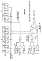
- the prior art circuitry is shown in Figure 1. This is essentially the same circuit shown in Figure 3 of US 4115 768.
- First and second series of flip-flops 10 and 14 operating as shift registers, are provided, and their outputs are linked to two groups of combinational logic gates 12 and 13.
- the output of gates 12 is supplied to the second series of flip-flops 14, as input, while the data to be encoded is the inputto the first series 10.
- the flip-flops of groups 10 and 14 are used as memory elements in this circuit because the data word cannot be fully encoded until its end is detected, i.e. it is essential to locate the end of a data word before one can properly encode it.
- the combinational logic circuitry shown generally at 12 and 13 performs this function.
- flip-flops are paired, i.e. flip-flops 28 with 18,30 with 20, 32 with 22, and so on, outputs from each one of each pair of flip-flops are used for the encoding, so that it is not apparent that, redundant circuit elements are present.
- inspection of the gating combinations made indicates that in each case the outputs from each flip-flop change on the rising edge of the clock pulses provided by +ESR CLOCK, but no effect on the encoding occurs until the clock pulse goes low again. Accordingly, while the flip-flop outputs change on alternate clock pulses, they are not used then, which allows the circuit to be simplified.
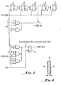
- Figure 2 shows an embodiment of the invention where simplification has been achieved. Note that only five flip-flops, numbered 33 to 37, replace the ten flip-flops shown in Figure 1. Their output signals A to E are generally equivalent to the signals B, D, F, H and J of Figure 1 and are inputs to combinational logic elements 40 and 41 which are also generally equivalent in function, though not in actual circuit design, to arrays 12 and 13 shown in Figure 1. Again, the combinational logic 40 and 41 uses all the outputs of the flip-flops 33-37.
- the inverted inputs to the logic elements, e.g., A may simply be the inverse outputs of the flip-flops 33-37, which are conventionally provided, i.e. A does not necessarily indicate a separate inversion operation performed on A.
- the output Y of the first group of combinational logic 40 feeds the second group of flip-flops 36 and 37, while the output X of the second group 41 is the encoded data stream.
- the output, on the line marked "Coded Data”, is the same for any given input series of data pulses as that obtained by the circuit of Figure 1.
- the output coded data is gated by a sixth flip-flop 42 at the 2F rate, i.e. at twice the data frequency F, in accordance with the rules of the encoding, according to which the coded data pulses are output at twice the rate at which the data to be encoded s input to the first flip-flop 33.
- one advantage of the paired flip-flops approach according to the known circuit is that race conditions, which can occur when the input to a flip-flop changes before the required holding time on the clock signal input has been satisfied, and can lead to data integrity problems, are generally avoided. If it should be desired to use a particular kind of flip-flop in which such a situation might prevail, race conditions may be avoided by including RC networks at 44 between succeeding flip-flops.
- the circuit will be implemented using so-called emitter-coupled logic (ECL) components, e.g. employing Signetics Model 10131 D-type flip-flops. The propagation delay of these circuits is 1.7 nanoseconds, and a clock hold time of 1.5 nanoseconds is required. Accordingly, the delay provided by the RC networks 44 is not needed.
- FIG 4 shows a cross- section of a circuit board in schematic form.
- the board comprises an insulative substrate 46 which may be made of an epoxy bonded fibreglass material.
- the conductors forming the circuitry of Figure 2 would be conductive material 48 bonded to one side of the circuit board 46.
- the other side of the circuit board is used for other circuitry such as power supply circuitry 50.
- a capacitance C typically exits between the power plane 50 and such conductors 48 and in many cases it can be a nuisance. According to this feature of the invention, the problems well known to be caused by such inherent capacitance are avoided, whle further hardware economies are realized.
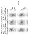
- Figure 3 shows an example of how an incoming data stream is converted to encoded data according to the rules discussed in US 3 689 899.
- the lower portion of Figure 3, labelled prior art, shows the signals output by the flip-flops 10 and 14 of Figure 1 at points A to J, and shows the signal Y which is the result of the operation of the upper portion 12 of the combinational logic in Figure 1, which is input to the second group of flip-flops 14.
- the ESR CLOCK pulse train is shown for clarity, as is the output encoded data.
- the upper portion of Figure 3 shows the same type of representation of signals in the circuit of the invention shown in Figure 2, wherein the lines A to E show the outputs of the flip-flops 33-37.
- Line Y shows the output of the upper portion of the combinational logic 41, as supplied to flip-flop 36, and the ENCODED DATA signal output by the circuit of the invention at flip-flop 42 is also shown.
- the uppermost portion of Figure 3 shows the incoming data stream at 52 and the encoded data at 54.
- the encoded data is also shown at 56, reclocked on the +2F clock frequency, which is desirable for reasons discussed below.
- the incoming data stream 52 is shown divided into words by single vertical lines and comprises a series of ones and zeroes. the first three word boundaries are noted on the drawing and are translated according to Table I given above, that is, 10 (line 52) translates to 0100 (lines 54-56) 010 translates to 100100, and so forth.
- the +ESR CLOCK signal is also shown topmost in Figure 3.
- US 4 115 768 also shows in Figures 6-8 a circuit for decoding data having been stored on a disk for supply to a host computer upon initiation of a read request, once again using paired flip-flops.
- the combinational logic 67 so that one flip-flop can be removed from each pair without affecting the function of the circuit and without modifying the logic circuitry.
- this would be the decoding circuitry employed, if a combination of sequenced flip-flops connected as shift registers and combinational logic were to be used as the decoding circuitry.
- Other decoding circuits are possible.
- the present circuit is desirably implemented using emitter-coupled logic (ECL).
- ECL emitter-coupled logic
- Previous decoding circuit such as Figure 1
- TTL transistor-transistor logic
- the best performance which could be achieved in tests of the circuit shown in Figure 1 was a data rate of 15 MHz whereas the simplified circuit of Figure 2 has been successfully tested up to 24 MHz using TTL circuitry, thus demonstrating a substantial speed advantage.
- An embodiment of the circuit of the invention using ECL circuitry is expected to run at up to 37.5 MHz data rate.
Landscapes
- Engineering & Computer Science (AREA)
- Signal Processing (AREA)
- Manipulation Of Pulses (AREA)
- Design And Manufacture Of Integrated Circuits (AREA)
- Logic Circuits (AREA)
- Dc Digital Transmission (AREA)
Description
- This invention relates to a circuit for encoding a stream of data pulses comprising a source of clock pulses for clocking data pulses through the circuit, afirst group of serially-connected flip-flops providing successively delayed versions of the data pulses, a second group of serially-connected flip-flops providing successively delayed versions of an intermediate signal, a first group of combinational logic elements responsive to selected outputs from the flip-flops to provide the intermediate signal, and a second group of combinational logic elements responsive to selected outputs from the flip-flops and the clock signals to provide an encoded signal.
- It has been known for some time that the efficiency of storage of digital data on magnetic storage media such as disks can be improved if the data is encoded prior to storage. The code generally used is such that the magnetic flux transitions written to the disk are encoded versions of the data written and do not correspond directly to the data. One such code which is in common use is the 2,7 run length limited code which is described in US Patent 3,689,899. Incoming data is scanned and specified patterns found in the data are converted in corresponding patterns of encoded ones and zeroes. According to this code, twice as many encoded bits are generated as data pulses are encoded. However, when the data is thereafter written to the disk, only the ones are written as magnetic flux transitions. This permits the encoded flux transitions to be written closer together, resulting in a net improvement in the amount of data which can be stored on a given disk. The encoded zeroes are represented by absences offluxtransitions, i.e. the space between adjacent flux transitions written to the disk is controlled by counting clock pulses supplied at a fixed frequency. Upon reading, the number of clock pulses counted between adjacent flux transitions is converted to a like number of zeroes between the ones represented by the flux transitions. The recovered encoded data can then be decoded, again according to US 3,689,899.
- A circuit of the type defined hereinbefore at the beginning for performing such encoding and decoding is shown in US Patent 4,115,768 and is in wide use in the data storage industry.
- The object of the invention is to provide a simplified, and therefore, less expensive and more reliable data encoding circuit.
- The invention is defined in
Claim 1 below. - The circuit shown in US 4 115 768 is greatly simplified by elimination of superfluous logic operations. In a preferred embodiment, the number offlip-flops used is cut substantially in half while the number of discrete logic gates is also reduced substantially. The circuit is capable of operation at significantly higher data rates than the known circuit.
- The invention will be described in more detail, by way of example, with reference to the accompanying drawings, in which:
- Figure 1 shows the prior art circuit found in US 4 115768;
- Figure 2 shows a corresponding schematic diagram of a circuit embodying the present invention;
- Figure 3 gives examples of encoding data by showing the signals at various points in the circuits of Figures 1 and 2; and
- Figure 4 shows a cross-sectional view of a portion of a circuit board.
- For ease in understanding of the present invention, the data patterns which are recognized and encoded by the encoding circuit of the invention and the encoded versions thereof, referred to above, are reproduced as Table I.

- Any desired combination of data to be stored can be generated from the data words listed in the left-hand column of Table I.
- It will be noted from examination of Table I that the code words are twice as long as the data words, but avoid the occurrence of 1's next to one another. In fact, according to the 2,7 "rules" of the code, any two adjacent flux transitions written to a disk representing 1's in the code words may be separated from one another by no less than two zeroes nor by more than seven zeroes. The written zeroes are counted upon later reading by comparison of the code words to a clock circuit. When a clock pulse goes by without a flux transition being detected on the disk, a zero is inserted in the stream of encoded data supplied to the decoding circuitry used, while the flux transitions are translated as ones. The "recovered" data can then be decoded; suitable decoding circuitry is fully described in US 4115 768 with reference to Figures 6-8 thereof.
- Encoding circuitry for conversion of the data words on the left-hand column of Table I into the code words is the area with which the present invention is cocerned. The prior art circuitry is shown in Figure 1. This is essentially the same circuit shown in Figure 3 of US 4115 768. First and second series of flip-
flops combinational logic gates gates 12 is supplied to the second series of flip-flops 14, as input, while the data to be encoded is the inputto thefirst series 10. The flip-flops ofgroups - It will be appreciated from a comparison of Figure 1 with Figure 3 of US 4 115 768 that the lines connecting the flip-
flops logic gates 12 are not drawn in Figure 1 of the present application, simply for clarity's sake. Instead, the outputs of the flip-flops are shown as signals A to J, and these letters identify the inputs to the combinational logic gates, as shown. Thus, for example, ANDgate 16 has as its inputs B, D, F, H and J. These are the inverted outputs of every other one of the groups of flip-flops flops first group 10, while H and J are the ouputs from flip-flops second group 14. Positive and inverted versions of the same clock signal "ESR CLOCK" are supplied to alternate ones of the flip-flops ingroups - While the flip-flops are paired, i.e. flip-
flops 28 with 18,30 with 20, 32 with 22, and so on, outputs from each one of each pair of flip-flops are used for the encoding, so that it is not apparent that, redundant circuit elements are present. However, inspection of the gating combinations made indicates that in each case the outputs from each flip-flop change on the rising edge of the clock pulses provided by +ESR CLOCK, but no effect on the encoding occurs until the clock pulse goes low again. Accordingly, while the flip-flop outputs change on alternate clock pulses, they are not used then, which allows the circuit to be simplified. Moreover, if outputs A, C, E, G and I are delayed half a clock period, but enabled as in US 4 115 768, i.e. upon raising of the following clock pulse, the outcome is unchanged. This indicates that half the flip-flops can be eliminated. - Figure 2 shows an embodiment of the invention where simplification has been achieved. Note that only five flip-flops, numbered 33 to 37, replace the ten flip-flops shown in Figure 1. Their output signals A to E are generally equivalent to the signals B, D, F, H and J of Figure 1 and are inputs to
combinational logic elements arrays combinational logic combinational logic 40 feeds the second group of flip-flops second group 41 is the encoded data stream. The output, on the line marked "Coded Data", is the same for any given input series of data pulses as that obtained by the circuit of Figure 1. Some of the simplification is achieved because there are only half as many flip-flops 33-37 to provide memory locations and accordingly thelogic - Further improvements are made using the Boolean identity


additional AND gates 43 from the known circuit. The output coded data is gated by a sixth flip-flop 42 at the 2F rate, i.e. at twice the data frequency F, in accordance with the rules of the encoding, according to which the coded data pulses are output at twice the rate at which the data to be encoded s input to the first flip-flop 33. - It will be appreciated that one advantage of the paired flip-flops approach according to the known circuit is that race conditions, which can occur when the input to a flip-flop changes before the required holding time on the clock signal input has been satisfied, and can lead to data integrity problems, are generally avoided. If it should be desired to use a particular kind of flip-flop in which such a situation might prevail, race conditions may be avoided by including RC networks at 44 between succeeding flip-flops. In the preferred embodiment, however, the circuit will be implemented using so-called emitter-coupled logic (ECL) components, e.g. employing Signetics Model 10131 D-type flip-flops. The propagation delay of these circuits is 1.7 nanoseconds, and a clock hold time of 1.5 nanoseconds is required. Accordingly, the delay provided by the RC networks 44 is not needed.
- Should RC networks 44 be required, however, the capacitors can be discrete or formed by the inherent capacitance between the conductors on the printed circuit board on which the circuit of the invention is realized and the power plane of the printed circuit board. Figure 4 shows a cross- section of a circuit board in schematic form. The board comprises an
insulative substrate 46 which may be made of an epoxy bonded fibreglass material. The conductors forming the circuitry of Figure 2 would beconductive material 48 bonded to one side of thecircuit board 46. Typically, the other side of the circuit board is used for other circuitry such aspower supply circuitry 50. A capacitance C typically exits between thepower plane 50 andsuch conductors 48 and in many cases it can be a nuisance. According to this feature of the invention, the problems well known to be caused by such inherent capacitance are avoided, whle further hardware economies are realized. - Figure 3 shows an example of how an incoming data stream is converted to encoded data according to the rules discussed in US 3 689 899. The lower portion of Figure 3, labelled prior art, shows the signals output by the flip-
flops upper portion 12 of the combinational logic in Figure 1, which is input to the second group of flip-flops 14. The ESR CLOCK pulse train is shown for clarity, as is the output encoded data. The upper portion of Figure 3 shows the same type of representation of signals in the circuit of the invention shown in Figure 2, wherein the lines A to E show the outputs of the flip-flops 33-37. Line Y shows the output of the upper portion of thecombinational logic 41, as supplied to flip-flop 36, and the ENCODED DATA signal output by the circuit of the invention at flip-flop 42 is also shown. The uppermost portion of Figure 3 shows the incoming data stream at 52 and the encoded data at 54. The encoded data is also shown at 56, reclocked on the +2F clock frequency, which is desirable for reasons discussed below. - The
incoming data stream 52 is shown divided into words by single vertical lines and comprises a series of ones and zeroes. the first three word boundaries are noted on the drawing and are translated according to Table I given above, that is, 10 (line 52) translates to 0100 (lines 54-56) 010 translates to 100100, and so forth. The +ESR CLOCK signal is also shown topmost in Figure 3. - Testing of the circuit shown in Figure 2 shows that it is indeed the function equivalent of the circuit shown in Figure 1 and produces the same encoded data in response to any given input data pattern.
- US 4 115 768 also shows in Figures 6-8 a circuit for decoding data having been stored on a disk for supply to a host computer upon initiation of a read request, once again using paired flip-flops. In this case, only the output from the second flip-flop of each pair is ever used by the combinational logic 67 so that one flip-flop can be removed from each pair without affecting the function of the circuit and without modifying the logic circuitry. In a preferred embodiment of a disk drive built according to the invention, this would be the decoding circuitry employed, if a combination of sequenced flip-flops connected as shift registers and combinational logic were to be used as the decoding circuitry. Other decoding circuits are possible.
- Signals in Figure 1 pass through differing numbers of differing types of gates which can lead to erroneous coding. All the signals in our circuit go through the same number of gates, by elimination of any gates equivalent to the AND
gates 43 of Figure 1 and all the gates in our circuit are the same type, i.e. NOR gates. Both these expedients add to reliability. Applicant's circuit also gates the output signal in the flip-flop 42, to avoid any "glitches" causes by these or other problems, such as variations in component tolerances. - There exists a trend in the data storage art toward higher and higher data rates. The present circuit, as noted, is desirably implemented using emitter-coupled logic (ECL). Previous decoding circuit such as Figure 1, was typically implemented using transistor-transistor logic (TTL) which is not as fast as emitter-coupled logic. The best performance which could be achieved in tests of the circuit shown in Figure 1 was a data rate of 15 MHz whereas the simplified circuit of Figure 2 has been successfully tested up to 24 MHz using TTL circuitry, thus demonstrating a substantial speed advantage. An embodiment of the circuit of the invention using ECL circuitry is expected to run at up to 37.5 MHz data rate.
- While a preferred embodiment of the invention has been described above, it will be appreciated that other embodiments are possible. For example, the embodiment shown uses NOR
gates
Claims (4)

Applications Claiming Priority (2)
| Application Number | Priority Date | Filing Date | Title |
|---|---|---|---|
| US06/444,158 US4484176A (en) | 1982-11-24 | 1982-11-24 | Run length limited data encoder |
| US444158 | 1982-11-24 |
Publications (3)
| Publication Number | Publication Date |
|---|---|
| EP0110625A2 EP0110625A2 (en) | 1984-06-13 |
| EP0110625A3 EP0110625A3 (en) | 1985-09-11 |
| EP0110625B1 true EP0110625B1 (en) | 1989-09-20 |
Family
ID=23763742
Family Applications (1)
| Application Number | Title | Priority Date | Filing Date |
|---|---|---|---|
| EP83307009A Expired EP0110625B1 (en) | 1982-11-24 | 1983-11-16 | Circuit for encoding data pulses |
Country Status (6)
| Country | Link |
|---|---|
| US (1) | US4484176A (en) |
| EP (1) | EP0110625B1 (en) |
| CA (1) | CA1203909A (en) |
| DE (2) | DE3390338T1 (en) |
| GB (1) | GB2140658A (en) |
| WO (1) | WO1984002237A1 (en) |
Families Citing this family (20)
| Publication number | Priority date | Publication date | Assignee | Title |
|---|---|---|---|---|
| JP2559354B2 (en) * | 1984-02-24 | 1996-12-04 | 株式会社日立製作所 | Digital signal modulation method |
| US4571575A (en) * | 1984-05-03 | 1986-02-18 | Sunol Systems Incorporated | Synchronization-promoting data coding method |
| US4757406A (en) * | 1985-09-13 | 1988-07-12 | Rodime Plc | High capacity disk drive |
| JPS62298234A (en) * | 1986-06-13 | 1987-12-25 | インタ−ナショナル ビジネス マシ−ンズ コ−ポレ−ション | Asymmetrical run length limited encoding |
| US4891717A (en) * | 1986-09-22 | 1990-01-02 | Magnetic Peripherals Inc. | Methods and apparatus for performing high density isotropic/perpendicular digital magnetic recording |
| NL8702903A (en) * | 1987-12-03 | 1989-07-03 | Philips Nv | METHOD AND APPARATUS FOR RECORDING INFORMATION ON A RECORD CARRIER, AND AN APPARATUS FOR READING THE RECORDED INFORMATION. |
| NL8702905A (en) * | 1987-12-03 | 1989-07-03 | Philips Nv | METHOD AND DEVICE FOR RECORDING INFORMATION, A RECORD BRACKET, A DEVICE FOR READING THE RECORDED INFORMATION, AND A CODING AND DECODING CIRCUIT FOR USE IN THE RECORDING AND READING DEVICE. |
| JPH01286626A (en) * | 1988-01-18 | 1989-11-17 | Hitachi Ltd | Data encoding system |
| US4979054A (en) * | 1988-02-25 | 1990-12-18 | Tandon Corporation | Disk drive for storing data in run length limited format and method of providing such format |
| US5184125A (en) * | 1989-06-28 | 1993-02-02 | Digital Equipment Corporation | Data encoding and demodulation system |
| JP2534778B2 (en) * | 1989-09-26 | 1996-09-18 | 株式会社日立製作所 | Information recording / reproducing system and information recording / reproducing apparatus |
| US5333126A (en) * | 1990-01-03 | 1994-07-26 | Hitachi, Ltd. | Information recording method and optical disk apparatus using same |
| JP3305344B2 (en) * | 1992-01-21 | 2002-07-22 | パイオニア株式会社 | Information recording / reproducing device using optical recording medium |
| US5422761A (en) * | 1992-11-20 | 1995-06-06 | International Business Machines Corporation | Disk drive with redundant recording |
| US5424881A (en) | 1993-02-01 | 1995-06-13 | Cirrus Logic, Inc. | Synchronous read channel |
| JP2863052B2 (en) | 1993-03-15 | 1999-03-03 | 松下電器産業株式会社 | Digital data encoding method, decoding method, encoding device, and decoding device |
| USRE40996E1 (en) | 1993-03-15 | 2009-11-24 | Panasonic Corporation | Optical recording disk capable of resynchronization in digital encoding and decoding |
| JPH0729307A (en) * | 1993-07-06 | 1995-01-31 | Eastman Kodak Co | System for recording and retrieving data in controlled-polarity method |
| US6959412B2 (en) * | 2002-03-04 | 2005-10-25 | Seagate Technology Llc | Error correction coding utilizing numerical base conversion for modulation coding |
| RU2476273C2 (en) * | 2011-04-12 | 2013-02-27 | Виталий Владимирович Соколов | Universal water-saving nozzle for water sprayers |
Family Cites Families (6)
| Publication number | Priority date | Publication date | Assignee | Title |
|---|---|---|---|---|
| US3689899A (en) * | 1971-06-07 | 1972-09-05 | Ibm | Run-length-limited variable-length coding with error propagation limitation |
| DE2508706C2 (en) * | 1974-05-02 | 1984-10-11 | International Business Machines Corp., Armonk, N.Y. | Circuit arrangement for coding data bit sequences |
| US3995264A (en) * | 1974-11-01 | 1976-11-30 | International Business Machines Corporation | Apparatus for encoding and decoding binary data in a modified zero modulation data code |
| US4146909A (en) * | 1977-11-21 | 1979-03-27 | International Business Machines Corporation | Sync pattern encoding system for run-length limited codes |
| US4408325A (en) * | 1980-11-28 | 1983-10-04 | Northern Telecom Limited | Transmitting additional signals using violations of a redundant code used for transmitting digital signals |
| US4413251A (en) * | 1981-07-16 | 1983-11-01 | International Business Machines Corporation | Method and apparatus for generating a noiseless sliding block code for a (1,7) channel with rate 2/3 |
-
1982
- 1982-11-24 US US06/444,158 patent/US4484176A/en not_active Expired - Lifetime
-
1983
- 1983-11-14 WO PCT/US1983/001774 patent/WO1984002237A1/en not_active Ceased
- 1983-11-14 DE DE19833390338 patent/DE3390338T1/en not_active Withdrawn
- 1983-11-14 GB GB08417622A patent/GB2140658A/en not_active Withdrawn
- 1983-11-16 DE DE8383307009T patent/DE3380607D1/en not_active Expired
- 1983-11-16 EP EP83307009A patent/EP0110625B1/en not_active Expired
- 1983-11-24 CA CA000441855A patent/CA1203909A/en not_active Expired
Also Published As
| Publication number | Publication date |
|---|---|
| US4484176A (en) | 1984-11-20 |
| GB2140658A (en) | 1984-11-28 |
| DE3390338T1 (en) | 1985-02-07 |
| EP0110625A3 (en) | 1985-09-11 |
| CA1203909A (en) | 1986-04-29 |
| EP0110625A2 (en) | 1984-06-13 |
| WO1984002237A1 (en) | 1984-06-07 |
| GB8417622D0 (en) | 1984-08-15 |
| DE3380607D1 (en) | 1989-10-26 |
Similar Documents
| Publication | Publication Date | Title |
|---|---|---|
| EP0110625A2 (en) | Circuit for encoding data pulses | |
| GB1578635A (en) | Dc free encoding for data transmission system | |
| US5481555A (en) | System and method for error detection and reducing simultaneous switching noise | |
| CA1102916A (en) | Sync pattern encoding system for run-length limited codes | |
| USRE31311E (en) | DC Free encoding for data transmission system | |
| GB2032227A (en) | D c free encoding for data transmission | |
| US5028922A (en) | Multiplexed encoder and decoder with address mark generation/check and precompensation circuits | |
| US3906485A (en) | Data coding circuits for encoded waveform with constrained charge accumulation | |
| US4245263A (en) | Write precompensation and write encoding for FM and MFM recording | |
| US4951049A (en) | Self clocking binary information encoder | |
| US4227184A (en) | Modified Miller Code encoder | |
| US4539680A (en) | Chip to chip information bit transmission process and device | |
| EP0122083B1 (en) | Method and apparatus for encoding a binary data stream into a binary code stream | |
| KR20010091311A (en) | Programmable frequency divider by high speed counter | |
| GB2095952A (en) | Bi-phase space code data signal reproducing circuit | |
| CN1073736C (en) | Error correcting memory system | |
| US4737765A (en) | 2,7 Code decoder with no more than 3 bits error propagation | |
| KR900000703B1 (en) | Parity detection circuit | |
| US3515994A (en) | Device for reproducing bivalent code elements registered in a moving signal carrier | |
| EP0064406A1 (en) | Encoding binary data | |
| JPS60500394A (en) | Improved run length limited data encoder | |
| JPH05258589A (en) | Variable length shift register | |
| US5841750A (en) | Information playback apparatus | |
| KR930010931B1 (en) | Data processing area assigning and control signal producing circuit and method of cd-rom system | |
| KR100230224B1 (en) | Scale Factor Majority Decision Circuit |
Legal Events
| Date | Code | Title | Description |
|---|---|---|---|
| PUAI | Public reference made under article 153(3) epc to a published international application that has entered the european phase |
Free format text: ORIGINAL CODE: 0009012 |
|
| AK | Designated contracting states |
Designated state(s): DE FR GB IT |
|
| PUAL | Search report despatched |
Free format text: ORIGINAL CODE: 0009013 |
|
| AK | Designated contracting states |
Designated state(s): DE FR GB IT |
|
| 17P | Request for examination filed |
Effective date: 19860224 |
|
| 17Q | First examination report despatched |
Effective date: 19870918 |
|
| GRAA | (expected) grant |
Free format text: ORIGINAL CODE: 0009210 |
|
| AK | Designated contracting states |
Kind code of ref document: B1 Designated state(s): DE FR GB IT |
|
| ITF | It: translation for a ep patent filed | ||
| REF | Corresponds to: |
Ref document number: 3380607 Country of ref document: DE Date of ref document: 19891026 |
|
| ITTA | It: last paid annual fee | ||
| PGFP | Annual fee paid to national office [announced via postgrant information from national office to epo] |
Ref country code: GB Payment date: 19891130 Year of fee payment: 7 Ref country code: FR Payment date: 19891130 Year of fee payment: 7 |
|
| ET | Fr: translation filed | ||
| PGFP | Annual fee paid to national office [announced via postgrant information from national office to epo] |
Ref country code: DE Payment date: 19900129 Year of fee payment: 7 |
|
| PLBE | No opposition filed within time limit |
Free format text: ORIGINAL CODE: 0009261 |
|
| STAA | Information on the status of an ep patent application or granted ep patent |
Free format text: STATUS: NO OPPOSITION FILED WITHIN TIME LIMIT |
|
| 26N | No opposition filed | ||
| PG25 | Lapsed in a contracting state [announced via postgrant information from national office to epo] |
Ref country code: GB Effective date: 19901116 |
|
| GBPC | Gb: european patent ceased through non-payment of renewal fee | ||
| PG25 | Lapsed in a contracting state [announced via postgrant information from national office to epo] |
Ref country code: FR Effective date: 19910731 |
|
| PG25 | Lapsed in a contracting state [announced via postgrant information from national office to epo] |
Ref country code: DE Effective date: 19910801 |
|
| REG | Reference to a national code |
Ref country code: FR Ref legal event code: ST |