EP0108346B1 - Memory reconfiguration method in a data processing system - Google Patents
Memory reconfiguration method in a data processing system Download PDFInfo
- Publication number
- EP0108346B1 EP0108346B1 EP83110751A EP83110751A EP0108346B1 EP 0108346 B1 EP0108346 B1 EP 0108346B1 EP 83110751 A EP83110751 A EP 83110751A EP 83110751 A EP83110751 A EP 83110751A EP 0108346 B1 EP0108346 B1 EP 0108346B1
- Authority
- EP
- European Patent Office
- Prior art keywords
- memory
- module
- locations
- blocks
- modules
- Prior art date
- Legal status (The legal status is an assumption and is not a legal conclusion. Google has not performed a legal analysis and makes no representation as to the accuracy of the status listed.)
- Expired
Links
Images



Classifications
-
- G—PHYSICS
- G06—COMPUTING OR CALCULATING; COUNTING
- G06F—ELECTRIC DIGITAL DATA PROCESSING
- G06F7/00—Methods or arrangements for processing data by operating upon the order or content of the data handled
-
- G—PHYSICS
- G06—COMPUTING OR CALCULATING; COUNTING
- G06F—ELECTRIC DIGITAL DATA PROCESSING
- G06F12/00—Accessing, addressing or allocating within memory systems or architectures
- G06F12/02—Addressing or allocation; Relocation
- G06F12/06—Addressing a physical block of locations, e.g. base addressing, module addressing, memory dedication
- G06F12/0646—Configuration or reconfiguration
- G06F12/0684—Configuration or reconfiguration with feedback, e.g. presence or absence of unit detected by addressing, overflow detection
-
- G—PHYSICS
- G06—COMPUTING OR CALCULATING; COUNTING
- G06F—ELECTRIC DIGITAL DATA PROCESSING
- G06F12/00—Accessing, addressing or allocating within memory systems or architectures
- G06F12/02—Addressing or allocation; Relocation
- G06F12/06—Addressing a physical block of locations, e.g. base addressing, module addressing, memory dedication
- G06F12/0646—Configuration or reconfiguration
- G06F12/0653—Configuration or reconfiguration with centralised address assignment
Definitions
- the present invention relates to a memory reconfiguration method in a data processing system.
- a memory module has a predetermined capacity (for instance 128K bytes) and is implemented with printed circuit boards of predetermined sizes and by a denoted number of standard integrated memory components. Because of rapid changes in technology, the manufacturers of data processing systems are faced with the problem of upgrading the working memory at minimum cost.
- a memory module may be built which has a greater capacity than it had (for instance double of quadruple) while at the same time maintaining the size of its memory board unchanged.
- the capacity of a working memory may be increased not only by increasing the number of memory modules, but also by utilizing memory modules of greater capacity.
- Prearranged circuits are required that can address any of several modules of the working memory so that the several modules may be addressed as if they constitute an addressable continuous space of one memory only.
- circuital solution proposed by such patent is partial since it is relatively slow and requires a considerable number of hardware components, so resulting complex and expensive.
- the modular memory sends to the central unit some information about the capacity of its constituting modules.
- the central unit processes such information and provides the memory with a set of information representative of the capacity of the first module, of the sum of the capacity of the first and second module, of the sum of the capacity of the first, second and third module, and so on to the total memory capacity.
- This information set is loaded into suitable registers of the module selection apparatus included into the memory.
- the signal representative of the results of the several comparisons are applied to a decoder which selects one of the several memory modules.
- module selection apparatus still comprises registers, comparison circuits and a decoder and therefore is relatively complex and slow too.
- US-A-3,958,222 discloses a module selection apparatus where the registers, comparison circuits and the decoder, are substituted with an associative memory or directory, which may be suitably preloaded, based on information related to the number of installed modules and their capacity, so as to provide conversion of an address code subset in a module selection signal.
- This apparatus is simpler and faster, but in order to avoid the need of additional hardware a method should be devised, for obtaining information on the number of installed modules and their capacity without resorting to additional hardware.
- a blank card has to be plugged instead of the additional storage card if the latter is not plugged, the blank card ensuring by its wiring that a predetermined storage location is addressed in lieu of a predetermined non existing storage location.
- the disclosed method has still some limitation in that is not intended for ascertaining the capacity of the additional storage card and further requires extra hardware in form of a blank card as a substitute for the additional card.
- the auxiliary memory acts as address translator, that is it produces a module selection signal from an absolute memory address.
- Each memory module can be considered as constituted by a certain number of ordered memory blocks having a prefixed basic capacity, for instance 64K words, that is each memory module may have a capacity equal to or multiple of 64K words.
- the memory physically constituted by modules, can be considered as ideally constituted by an ordered plurality of M memory blocks.
- the auxiliary memory or directory has a number of memory locations at least equal to the maximum number of memory blocks which may constitute the working memory.
- each memory block can be associated to one directory location.
- the memory blocks are shared among the several possible memory modules, each module being able to contain at the most N blocks.
- the memory addressing is performed in binary form.
- a memory address is constituted by a suitable number of bits. The less significant bits, for instance 16 bits in case of memory blocks with capacity of 664K words, allow to identify an address within a block.
- a portion of the most significant bit allows to identify the memory block which the address relates to.
- the loading operations of the directory with the information relation to the modules containing the memory blocks are executed by the central unit at the initialization or the reconfiguration of the system according to a method which constitutes the object of the present invention.
- the central unit loads the directory locations corresponding to the several memory blocks with a coded information selecting a first module J.
- the central unit addresses through the auxiliary memory or directory a predetermined location of each of the memory blocks and, by means of writing, reading and comparison operations, verifies the belonging of each block to module J.
- Figure 1 shows in schematic block diagram a data processing system wherein the memory reconfiguration method of the present invention may be used.
- the system of figure 1 comprises a central processing unit 1 and working memory 2 interconnected through a channel 3 constituted by a plurality of leads.
- central unit 1 may send to memory 2 timing signals, commands, addresses, data to be written and may receive from memory 2 read data and status information.
- Central unit 1 is provided with a microprogram- med control unit, an operative unit, a plurality of working registers and a suitable interface with channel 3.
- central unit 1 and channel 3 For the invention purposes any additional information about central unit 1 and channel 3 is unnecessary because the invention may be used with every type of central unit and of interconnection channel.
- Working memory 2 includes an interface and module selection unit 4 and a plurality of memory modules which may be installed in variable number from 1 to a maximum of 4 (M0, M1, M2, M3) into corresponding ordered housings (H0, H1, H2, H3) of the memory structure.
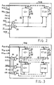
- FIGS 2 and 3 show some examples of possible embodiments of different capacity memory modules.
- Figure 2 shows a memory module of capacity 64K words.
- It is constituted by a printed circuit board PWB on which twenty integrated memory circuits C11, ..., CI20 are arranged to form a row.
- the memory parallelism be of 20 bits, of which 16 bits are used as information bits and 4 bits as redundant bits of check and error correction.
- Each integrated circuit On may be of the type with capacity 64K bits available on the market (for instance circuit HM 4864-2 manufactured by HITACHI) and requires 16 addressing bits.
- the memory addressing is executed according to the well known multiplexing method in two subsequent phases.
- the addressing of a cell is performed by selecting at first a matrix row with an 8-bit code validated by command RS and then a matrix column with an 8-bit code validated by commandCS.
- the memory operation which is executed is a reading or writing operation according to the logical level of the signal applied to input R/W of the integrated circuit.
- Output DO of the memory integrated circuit is of tristate type.
- Such output normally held in high impedance state, goes to logical level 1 or 0, according to the information stored in the selected cell, only during the reading operations and for a pre-established time interval after command CS has been received.
- the interface connecting the module of fig. 2 to unit 4 of fig. 1 is very simple and comprises:
- Fig. 2 shows that the transfer of signals RS, CS from pins RAS, CAS to the corresponding inputs of the module integrated circuits is conditioned by two logical gates 23, 24 enabled by the signal present on module selection pin Si.
- the module interface is provided with two additional pins A16, A17 which are not used in the module of fig. 2.
- the printed circuit board of the memory module may be arranged to contain two rows of integrated circuits of the same type previously described.
- the memory module capacity is 128K words.
- Fig. 3 schematically shows, with the same simplifications of fig. 2, a module of capacity 128K words obtained by arranging on the printed circuit boards two rows of memory integrated circuits.
- Output of NAND gate 25 is coupled to inputs CS of the integrated circuits of the first row.
- Output of NAND gate 27 is coupled to inputs CS of the integrated circuits of the second row.
- Pins Si and RAS are also connected to the inputs of a NAND gate 26 whose output is coupled to inputs RS of the integrated circuits of both first and second row.
- the signal on pin A16 allows to select during the read/write operations one of the two rows of integrated circuits.
- Such circuits differ from the previous ones only because addressing input A8 is here really used for selecting one of two sets of 256 columns inside the integrated circuit.
- modules of fig. 2 and 3 one or two rows of such integrated circuits may be respectively installed so as to obtain a module of capacity 128K words and 256K words respectively.
- input A8 of integrated circuits is connected to pin A16 of the printed circuit.
- input A8 is connected to pin A17 and the logical circuits selecting the row of integrated circuits remain unchanged.
- the memory modules do not provide unit 4 of fig. 1 with any information about their capacity. It is also to be noted that, if such modules have a capacity less than the possible maximum one of 4 blocks and are selected with signal Siand an address greater than the installed capacity, they neglect the most significant bits of the address, as for instance that ones applied to inputs A16, A17. This involves erroneous addressing and overwriting operations.
- the module have a capacity of 64K words corresponding to one only memory block and be addressed with a binary code 0 corresponding to the first location of the block in order that an information A be written into such location.
- Fig. 4 shows an example of embodiment of circuit which selects a memory block within a module and prevents the information overwriting.
- the selection circuit comprises five 2-input NAND gates 29,33,34,35,36, a 2-input AND gate 30 and two NOT gates 31, 32.
- NAND gate 29 The inputs of NAND gate 29 are respectively connected to pins RAS and Si of the module interface.
- Output of NAND 29 is connected through lead 37 to inputs% of the module integrated circuits.
- the inputs of AND gate 30 are respectively connected to pins Si and CAS of the module interface.
- Output of AND gate 30 is connected to an input of each of NAND gates 33, 34, 35, 36.
- Pin A16 is connected to an input of NAND gate 33 and, through NOT gate 31, to an input of NAND gate 34.
- pin A16 is further connected, through lead 38, to pin A8 of such integrated circuits.
- Pin A17 is connected to an input of NAND gate 35 and, through NOT gate 32, to an input of NAND gate 36.
- Outputs of NAND gate 33, 34 provide respectively signals CSI and CSII which are used as column strobes CS respectively for the first and the second row of integrated circuits of capacity 64K bits possibly installed in the module.
- Outputs of NAND gates 35, 36 provide respectively signais CSI and CSII which are used as column strobes CS respectively for the first and second row of integrated circuits capacity 128K bits possibly installed in the module.
- command ⁇ S sent to the several integrated circuits, is conditioned by the addressing code.
- the installed integrated circuits do not receive command CS and therefore the memory operation is not performed, that is overwriting is avoided.
- the capacity of each of the memory modules may be therefore chosen among several values, that is 64K words, 128K words, 256K words.
- the total memory capacity may vary from 64K to 1 M words for multiples of 64K words, with the only exception of 960K words.
- Each memory module of capacity greater than 64K, that is 128K and 256K, may be considered as constituted respectively by two and four memory blocks of basic capacity 64K.
- the memory may be considered as constituted by a plurality of blocks shared among several modules.
- Central unit 1 can therefore address a word stored into memory 2 with a binary code of 20 bits A 00-19.
- bits A16-19 are used to specify one of the possible 16 memory blocks of 64K words, whilst the 16 less significant bits A 00-15 are used to address a word within the specified block.
- each module must receive 18 addressing bits A 00-17.
- Fig. 5 shows more in detail working memory 2 and more particularly, module selection and interface unit 4.
- Unit 4 receives through channel 3 a suitable information set.
- Channel 3 comprises a plurality of leads:
- the central unit Contemporaneously with the generation of command START MM, the central unit puts on leads ADD/DATA a binary code representative of the memory location to be addressed;
- the central unit When the central unit receives signal CK1, it puts on leads ADD/DATA, in case of a memory writing operation, some information representative of the datum to be written into memory or, in case of a memory reading operation, it prepares itself for receiving from leads ADD/ DATA information read out from memory;
- the set of leads COMM is coupled to the inputs of a register CREG 5 which receives at its enabling input signal START MM.
- Unit 4 comprises a timing unit 7 which receives at its enabling input signal START MM.
- Timing unit 7 provides on its outputs, besides signals CK1 and ENCY already seen, also signals RAS, CK2, CAS, CK3.
- Timing unit 7 may be embodied in several ways; they are known to the people skilled in the art and are unessential for the invention purposes.
- timing unit 7 Any description of timing unit 7 is therefore omitted.
- Neglecting signals CK1, ENCY already considered the meaning of signals RAS, CK2, CAS, CK3 is the following:
- such signal when active, allows during a memory writing operation to put on the memory input data channel the information related to the datum to be written.
- Fig. 6 shows as a qualitative example the timing diagram of signals START MM, CK1, RAS, CK2, CAS, CK3, ENCY.
- the set of bidirectional leads ADD/DATA is coupled to the outputs of a register DBREG 15 (for instance of the type marketed with code 74S374).
- registerD0REG 15 are connected to channel D0 of data output from the several memory modules M0, ... M3.
- Output control pin OC of register D0REG 15 is connected to the output of a NAND gate 15A which receives at its inputs signal CK3 and signal R/W coming from an output of decoder 6 and indicating when at logical level 1(0) a memory reading (writing) operation.
- the set of bidirectional leads ADD/DATA is further coupled to the inputs of a register ADD REG 16 which receives at its enabling input signal START MM.
- Bidirectional leads ADD/DATA are further connected to the inputs of a register DI REG 17, whose enabling input is coupled to the output of an AND gate 14.
- AND gate 14 receives at a first input signal CK2 and at a second input, through a NOT gate 19, signal R/W in output from decoder 6.
- Outputs of register 17 are coupled to data input channel DI of the several memory modules.
- the outputs of register ADD REG 16 related to address bits AOQ-07 and A08-15 are respectively connected to a first and second input set of a multiplexer 18.
- the outputs of multiplexer 18 and the outputs of register 16 related to address bits A16, A17 are coupled to addressing channel 16A of modules MO,... M3.
- Multiplexer 18 receives at its selection input signal CK2. According to the logical level of signal CK2, multiplexer 18 transfers to its outputs the information present on Q ne of its two input sets; in particular:
- unit 4 for the purposes of the present invention is the presence of a fast auxiliary memory or directory 19 having a number of memory locations at least equal to the maximum number of memory blocks of basic capacity 64K words and a parallelism equal to the maximum number of foreseen modules.
- the auxiliary memory 19 has 16 memory locations with parallelism 4 bits.
- 16x4 bit memory circuit marketed with code 74F189 by firm FAIRCHILD and with typical access time of 20 nsec may be used.
- Such memory circuit is of inverting type, that is the information received at its inputs is stored and therefore read out in negated form.
- Outputs of memory 19 are of open collector type.
- Memory 19 is further provided with an enabling input and a read/write control input.
- Outputs D0-03 of directory 19 are coupled each to a voltage source +V through a pull-up resistor.
- a signal CK1 obtained by inverting CK1 through a NOT 21, is applied to enabling input of directory 19.
- a signel W DIR present on one output of decoder 6 is applied to read/write control input of directory 19.
- the four data inputs DIO-3 of directory 19 are coupled to four suitable outputs of register DI REG 17 through a NOT gate set 20 so that directory 19 and NOT gate set 20 may be considered as a non inverting directory.
- the four addressing inputs AO... A3 of directory 19 are connected to outputs A16, A17, A18, A19 of register ADD REG 16, that is to the outputs related to the most significant bits of a memory address.
- Outputs D0 0-3 of directory 19 are respectively connected to selection pins SO ..., S3 of modules M0, ..., M3.
- Such outputs are further coupled to the inputs of a 4-input NOR gate 22.
- NOR gate 22 generates on its output signal OVERM at logical level 1 when all the signals present on its inputs are at the same time at logical level 0.
- Signal OVERM is sent to central unit 1 and shows that the memory address received by unit 4 exceeds the memory capacity.
- modules M0, M1, M2, M3 receive signals RIW, RAS, CAS, too.
- the working of the module selection apparatus of unit 4 is very simple.
- the central unit through a method which will be explained more in detail later on and which properly constitutes the object of the invention, performs a mapping of directory 19.
- the central unit provides to write into each location i(0 ⁇ i ⁇ 15) of directory 19 an information which selects module Mj (0 ⁇ j ⁇ 3) containing the memory block of basic capacity coupled to location i.
- the working memory includes modules MO of capacity 256K words, module M2 of capacity 128K words and module M4 of capacity 64K words (therefore the total memory capacity is 448K words, that is equal to 7 memory blocks each of 64K words), the content of the several locations of directory 19 is given by the following table:
- the information herein stored selects memory module M2 containing the 5th memory block inside which the memory location of address 300K is present.
- the module activation occurs with timing signals RAS which must have a delay as regards the rising edge of signal CK1 equal to the maximum access time of directory 19.
- the module selection delay with regard to the time when the row addressing bits are available to the inputs of the same module may be reduced at a minimum.
- the circuital structure of the selection network is very simple and unexpensive because all the logical networks of sum, subtraction and comparison, used in the selection networks of the prior art, are abolished, the directory mapping operation being assigned to the central unit and executed once for all during the system initialization or during a possible memory reconfiguration owing to an addition/removal/substitution of memory modules.
- Any central unit provided with an internal control memory or with a program memory anyhow different from that one to be mapped, as well as with a reduced number of working registers which may be also memory locations, provided they do not belong to the memory to be mapped, is able to perform the mapping operations of the invention by means of a very simple program or microprogram.
- mapping is performed according to the following method.
- the directory is written so as to select in any way a hypothetical first module.
- test codes Some arbitrary test codes are written into such addressed memory locations; these codes are then read.
- Such code is used to generate signal OVERM when these remaining locations are addressed.
- the eight columns of the above table are related to four hypothetical memory module capacities, that is respectively 0 (missing module), 64K, 128K, 256K.
- the three rows of the above table are related to three writing addresses, that is respectively 0 (first module location), 64K (first location exceeding the capacity of a memory block) and 128K (first location exceeding the capacity of 2 memory blocks).
- Addresses 0, 64K, 128K are represented by a binary code whose bits A00-15 are all zeroes and bits A17, A16 are respectively 00 for address 0, 01 for address 64K, 10 for address 128K.
- mapping method provides for the writing into a hypothetical module of a test code A at address 0, of a test code B at address 64K, of a test code C at address 128K.
- the module has a capacity 64K and is such that overwriting occurs, only location of address 0 is involved in the writing operations and the content of it is C.
- the module has a capacity of 128K and is such that overwriting occurs, only locations of address 0, 64K are involved in the writing operations and the content of them is C, B respectively.
- the module has a capacity of 256K, the content of locations of addresses 0, 64K, 128K is A, B, C respectively.
- the additional following table shows the information which are read out from a memory module, written as previously mentioned, when such module is addressed with the same addresses used for the test code writing. In case of module without any possibility of overwriting, when a missing location is addressed, the read information is 0.
- module location of address 0 the module is missing; if on the contrary it is different from 0, the module is present.
- the module capacity is 64K; if on the contrary it is different from 0 to C, the module capacity is greater than 64K.
- the content of module location of address 128K is read out. If the read information is 0, the module capacity is 128K (with regard to module overwriting); if on the contrary it is different from 0 the module may have a capacity of 128K (with regard to module with overwriting) or a greater capacity, that is 256K.
- the module capacity is 128K.
- Such figures contains the words CNT (counter) SCREG (selecting register) MAREG (memory addressing register), DAREG (directory addressing register) which are indicative of some registers of central unit 1 which are used during the memory mapping method.
- the central unit resets its internal register CNT, loads its internal register SCREG with a code 0001 devoted to select memory module MO and its internal register MAREG with an address 0 devoted to select the first location of the first memory block of capacity 64K words (diagram block 101).
- the central unit After having transferred the content of MAREG related to addressing bits 16-19 into DA REG (diagram block 102), the central unit writes the contents of SCREG into the directory location DIR specified by the content of DAREG (diagram block 103).
- central unit provides to increment by one unit the content of DA REG (diagram block 104) and to check if such content is equal to 16 (expressed in binary code), that is to the maximum foreseen number of memory blocks (diagram block 105).
- the central unit cyclically repeats the operations described by diagram blocks 103, 104, 105.
- the central unit checks if the content of register CNT is equal to 4 (diagram block 106).
- the central unit provides to write a test code A, B, C, into memory locations addressed by content of MAREG, by content of MAREG+64K and by content of MAREG+128K respectively (diagram block 107). Then the central unit reads the memory location addressed by content of MAREG and loads a register W with the read information (diagram block 108).
- the central unit executes a reading operation at memory address MAREG+64K and loads register W with the read information (diagram block 110).
- the central unit checks if the read information is equal to or different from C.
- the central unit suitably verifies that the read information is not affected by a parity error (diagram block 112).
- This error could be due to a defect or damage of the addressed memory location.
- the program jumps to diagram block 121, that is the content of MAREG is incremented by one unit, and then returns to diagram block 102.
- the central unit reads the memory location of address MAREG+128K and loads register W with the read information (diagram block 114). If the read information is equal to 0, the selected module has capacity 128K and the program jumps to diagram block 120.
- the central unit reads the memory location of address MAREG (diagram block 115A) and verifies that the related information is not affected with error for the already cited reasons (diagram block 116).
- the central unit therefore increments the content of MAREG by 256K (diagram block 117), then increments by one unit the content of CNT and shifts left the content of SCREG (diagram block 118).
- MAREG is incremented by 64K or by 128K respectively (diagram blocks 119, 120).
- the checking of the performed counting operations puts an end to the mapping program.
- the program can be considerably simplified and an only test code can be used.
- test codes instead of different test codes, an only test code can be used if such code is written into and again read out from memory locations whose addresses differ each other not only for the most significant bits but also for one or several less significant bits.
Landscapes
- Engineering & Computer Science (AREA)
- Theoretical Computer Science (AREA)
- Physics & Mathematics (AREA)
- General Engineering & Computer Science (AREA)
- General Physics & Mathematics (AREA)
- Techniques For Improving Reliability Of Storages (AREA)
- Logic Circuits (AREA)
Description
- The present invention relates to a memory reconfiguration method in a data processing system.
- Most data processing systems presently used provide the opportunity for increasing the capacity of the working memory in order to fulfill new requirements.
- This is commonly attained by arranging the working memory modularly, that is by having a variable number of identical memory modules housed into a unit which is designed to contain a certain maximum number of modules.
- A memory module has a predetermined capacity (for
instance 128K bytes) and is implemented with printed circuit boards of predetermined sizes and by a denoted number of standard integrated memory components. Because of rapid changes in technology, the manufacturers of data processing systems are faced with the problem of upgrading the working memory at minimum cost. - Because of such progress in new integrated memory components which have greater and greater capacity, a memory module may be built which has a greater capacity than it had (for instance double of quadruple) while at the same time maintaining the size of its memory board unchanged. Thus the capacity of a working memory may be increased not only by increasing the number of memory modules, but also by utilizing memory modules of greater capacity.
- Moreover, it is unnecessary to remove the fewer capacity modules already installed.
- In such a way it is possible to obtain a working memory with a capacity variable as a function of the number and type of modules, and in which modules of different capacity are present at the same time.
- However there is a problem in addressing such memories.
- Prearranged circuits are required that can address any of several modules of the working memory so that the several modules may be addressed as if they constitute an addressable continuous space of one memory only.
- Because in data processing systems processors, working memories and peripheral units are all interconnected via busses which define a common interface for several types of equipments, it is not possible to perform the required address conversion outside the working memory without affecting the interfaces of all the equipment.
- Such conversion must therefore occur within the working memory and must be performed with simple and fast circuits so as not to introduce unacceptable delays in the memory access times and further increase the complexity and the related cost of such circuits.
- A partial solution to this problem is described in U.S. Patent number 4,001,786.
- The circuital solution proposed by such patent is partial since it is relatively slow and requires a considerable number of hardware components, so resulting complex and expensive.
- U.S. Patent Application No. 422,772 filed by the same Applicant on September 24, 1982 (or the corresponding European Patent Application No. 82110396.7 published with No: 0080626 on June 8, 1983) describes a memory module selection apparatus which uses a logical selection network simpler and faster than the one described in the mentioned U.S. Patent.
- In fact certain processing functions are devolved on the central unit, which performs them once for all during the initialization phase.
- In particular the modular memory sends to the central unit some information about the capacity of its constituting modules.
- The central unit processes such information and provides the memory with a set of information representative of the capacity of the first module, of the sum of the capacity of the first and second module, of the sum of the capacity of the first, second and third module, and so on to the total memory capacity.
- This information set is loaded into suitable registers of the module selection apparatus included into the memory.
- When the memory is addressed, a meaningful portion of the address is at the same time compared, by several comparators, with the content of the several registers.
- The signal representative of the results of the several comparisons are applied to a decoder which selects one of the several memory modules.
- But the above mentioned module selection apparatus still comprises registers, comparison circuits and a decoder and therefore is relatively complex and slow too.
- US-A-3,958,222 discloses a module selection apparatus where the registers, comparison circuits and the decoder, are substituted with an associative memory or directory, which may be suitably preloaded, based on information related to the number of installed modules and their capacity, so as to provide conversion of an address code subset in a module selection signal.
- This apparatus is simpler and faster, but in order to avoid the need of additional hardware a method should be devised, for obtaining information on the number of installed modules and their capacity without resorting to additional hardware.
- For instance, in the IBM Technical Disclosure Bulletin, Vol 15, No 12, May 1975 page 3796 there is described a method for detecting the presence or absence of an additional storage card of known capacity. There is proposed to increase the memory capacity of a control store, beyond a nominal value, by plugging an additional storage card and to detect the presence or absence of the additional storage card by means of memory read write operations performed at addresses within and beyond the nominal capacity value, to detect if overwriting of the same memory location occurs.
- A blank card, has to be plugged instead of the additional storage card if the latter is not plugged, the blank card ensuring by its wiring that a predetermined storage location is addressed in lieu of a predetermined non existing storage location.
- The disclosed method has still some limitation in that is not intended for ascertaining the capacity of the additional storage card and further requires extra hardware in form of a blank card as a substitute for the additional card.
- These disadvantages are overcome by the method of the present invention as claimed which allows to use a still more reduced number of hardware components and to reduce to a minimum the module selection delays. Such advantages are obtained by devolving on the system central unit suitable processing functions, the computation of the capacity of each memory module included, and by using an auxiliary read/ write selection memory or directory loaded by the same central unit of the system.
- The auxiliary memory, once loaded, acts as address translator, that is it produces a module selection signal from an absolute memory address. Each memory module can be considered as constituted by a certain number of ordered memory blocks having a prefixed basic capacity, for
instance 64K words, that is each memory module may have a capacity equal to or multiple of 64K words. - Therefore the memory, physically constituted by modules, can be considered as ideally constituted by an ordered plurality of M memory blocks. The auxiliary memory or directory has a number of memory locations at least equal to the maximum number of memory blocks which may constitute the working memory.
- In such a way each memory block can be associated to one directory location.
- The memory blocks are shared among the several possible memory modules, each module being able to contain at the most N blocks. As known, the memory addressing is performed in binary form. A memory address is constituted by a suitable number of bits. The less significant bits, for
instance 16 bits in case of memory blocks with capacity of 664K words, allow to identify an address within a block. - A portion of the most significant bit allows to identify the memory block which the address relates to.
- Besides the most significant bits are used to address the directory location wherein a coded information representative of the module containing the specified memory block is stored.
- Therefore such coded information allows to select the suitable memory module during the addressing operations of the system memory.
- The loading operations of the directory with the information relation to the modules containing the memory blocks are executed by the central unit at the initialization or the reconfiguration of the system according to a method which constitutes the object of the present invention.
- With regard to such method, the central unit loads the directory locations corresponding to the several memory blocks with a coded information selecting a first module J.
- Then the central unit addresses through the auxiliary memory or directory a predetermined location of each of the memory blocks and, by means of writing, reading and comparison operations, verifies the belonging of each block to module J.
- If the blocks, in all or in part, do not belong to module J, the central unit executes some operations similar to the ones previously described and checks if such blocks belong to module J+1, and so on. These and other features will appear clearer from the following description of a preferred embodiment of the invention and from the enclosed drawings where:
- -Figure 1 is the schematic block diagram of a data processing system wherein the method of the invention may be used;
- -Figures 2 and 3 show the wiring. diagram of different capacity memory modules which may be used in the system of fig. 1;
- -Figure 4.shows a selection circuit which may be used in the system of fig. 1 inside a memory module;
- -Figure 5 shows in detail an interface and module selection unit of the system of fig. 1;
- -Figure 6 shows in quantitative timing diagram some timing signals used by the unit of fig. 5;
- -Figures 7 and 8 are a logic flow diagram of a program according to which the method of the invention is developed.
- Figure 1 shows in schematic block diagram a data processing system wherein the memory reconfiguration method of the present invention may be used. The system of figure 1 comprises a
central processing unit 1 andworking memory 2 interconnected through a channel 3 constituted by a plurality of leads. - Through channel 3,
central unit 1 may send tomemory 2 timing signals, commands, addresses, data to be written and may receive frommemory 2 read data and status information. -
Central unit 1 is provided with a microprogram- med control unit, an operative unit, a plurality of working registers and a suitable interface with channel 3. - For the invention purposes any additional information about
central unit 1 and channel 3 is unnecessary because the invention may be used with every type of central unit and of interconnection channel. -
Working memory 2 includes an interface andmodule selection unit 4 and a plurality of memory modules which may be installed in variable number from 1 to a maximum of 4 (M0, M1, M2, M3) into corresponding ordered housings (H0, H1, H2, H3) of the memory structure. - Figures 2 and 3 show some examples of possible embodiments of different capacity memory modules.
- Figure 2 shows a memory module of
capacity 64K words. - It is constituted by a printed circuit board PWB on which twenty integrated memory circuits C11, ..., CI20 are arranged to form a row. In other words assumption is made that the memory parallelism be of 20 bits, of which 16 bits are used as information bits and 4 bits as redundant bits of check and error correction.
- Each integrated circuit On may be of the type with
capacity 64K bits available on the market (for instance circuit HM 4864-2 manufactured by HITACHI) and requires 16 addressing bits. - It is provided with a data input DI, a data output DO, timing and command inputs RS and CS, a readwrite command input R/W and 8 addressing inputs AO-7.
- The memory addressing is executed according to the well known multiplexing method in two subsequent phases.
- As memory cells inside the integrated circuit are ideally arranged according to a matrix of 256 rows and 256 columns, the addressing of a cell is performed by selecting at first a matrix row with an 8-bit code validated by command
RS and then a matrix column with an 8-bit code validated by commandCS. - Besides the memory integrated circuit is provided with an input A8 not used.
- The memory operation which is executed is a reading or writing operation according to the logical level of the signal applied to input R/W of the integrated circuit.
- Output DO of the memory integrated circuit is of tristate type.
- Such output, normally held in high impedance state, goes to
logical level - Further information about such memory integrated circuits can be found in the manufacturer data books.
- The interface connecting the module of fig. 2 to
unit 4 of fig. 1 is very simple and comprises: - -a set DI 00-19 of 20 pins for sending data to the module,
- -a set DO 00-19 of 20pins for receiving data from the module,
- two pins RAS, CAS for sending commands RS, CS to the module,
- -a pin R/W for sending a homonymous command to the module,
- -a pin Si for sending a selection command to the module,
- -a set of 8 pins A 00-07 for sending row and column addresses to the module.
- The connections between pins DI 00-19 (DO 00-19) and inputs DI (DO) of the several integrated circuits are not shown for drawing simplicity and clearness and also because they are obvious.
- Fig. 2 shows that the transfer of signals RS, CS from pins RAS, CAS to the corresponding inputs of the module integrated circuits is conditioned by two
logical gates - The module interface is provided with two additional pins A16, A17 which are not used in the module of fig. 2.
- In fact the printed circuit board of the memory module may be arranged to contain two rows of integrated circuits of the same type previously described.
- In such case the memory module capacity is 128K words.
- Therefore it is essential to have a further addressing bit which is transferred through one of the two additional pins, for instance pin A16.
- Fig. 3 schematically shows, with the same simplifications of fig. 2, a module of
capacity 128K words obtained by arranging on the printed circuit boards two rows of memory integrated circuits. - In this case the logical signal on pin A16 is applied, through a
NOT gate 28, to an input of a 3-input NAND gate 25. - Output of
NAND gate 25 is coupled to inputs CS of the integrated circuits of the first row. - Besides the logical signal on pin A16 is applied to an input of a second 3-
input NAND gate 27. - Output of
NAND gate 27 is coupled to inputs CS of the integrated circuits of the second row. - The other two inputs of both
NAND gates - Pins Si and RAS are also connected to the inputs of a
NAND gate 26 whose output is coupled to inputs RS of the integrated circuits of both first and second row. - By means of such selection circuit the signal on pin A16 allows to select during the read/write operations one of the two rows of integrated circuits.
- Besides memory integrated circuits with
capacity 128K bits are foreseen to be put on the market. - Such circuits differ from the previous ones only because addressing input A8 is here really used for selecting one of two sets of 256 columns inside the integrated circuit.
- It is therefore clear that in the modules of fig. 2 and 3 one or two rows of such integrated circuits may be respectively installed so as to obtain a module of
capacity 128K words and 256K words respectively. In the first case input A8 of integrated circuits is connected to pin A16 of the printed circuit. - In the second case input A8 is connected to pin A17 and the logical circuits selecting the row of integrated circuits remain unchanged. It is to be noted that the memory modules do not provide
unit 4 of fig. 1 with any information about their capacity. It is also to be noted that, if such modules have a capacity less than the possible maximum one of 4 blocks and are selected with signal Siand an address greater than the installed capacity, they neglect the most significant bits of the address, as for instance that ones applied to inputs A16, A17. This involves erroneous addressing and overwriting operations. - Assumption be made for instance that the module have a capacity of 64K words corresponding to one only memory block and be addressed with a
binary code 0 corresponding to the first location of the block in order that an information A be written into such location. - If the same module is successively addressed with a 17-bit binary code 10000000000000000 corresponding to the location of
address 64K in order that an information B be written into such location, the location really addressed is the location ofaddress 0 and information B is here written and therefore replaces information A previously stored. - This remark is essential for understanding the memory mapping method which will be described later on.
- It is to be pointed out that figures 2 and 3 only show some examples of possible embodiments of memory modules.
- Fig. 4 shows an example of embodiment of circuit which selects a memory block within a module and prevents the information overwriting. The selection circuit comprises five 2-
input NAND gates gate 30 and twoNOT gates - The inputs of
NAND gate 29 are respectively connected to pins RAS and Si of the module interface. - Output of
NAND 29 is connected throughlead 37 to inputs% of the module integrated circuits. - The inputs of AND
gate 30 are respectively connected to pins Si and CAS of the module interface. - Output of AND
gate 30 is connected to an input of each ofNAND gates - Pin A16 is connected to an input of
NAND gate 33 and, throughNOT gate 31, to an input ofNAND gate 34. - In case the memory module is constituted by integrated circuits with
capacity 128K bits, pin A16 is further connected, throughlead 38, to pin A8 of such integrated circuits. - Pin A17 is connected to an input of
NAND gate 35 and, throughNOT gate 32, to an input ofNAND gate 36. - Outputs of
NAND gate CSI andCSII which are used as column strobes CS respectively for the first and the second row of integrated circuits ofcapacity 64K bits possibly installed in the module. - Outputs of
NAND gates CSI andCSII which are used as column strobes CS respectively for the first and second row ofintegrated circuits capacity 128K bits possibly installed in the module. - By means of such selection circuit, command ëS, sent to the several integrated circuits, is conditioned by the addressing code.
- If the memory addressing code exceeds the capacity of the module, the installed integrated circuits do not receive command
CS and therefore the memory operation is not performed, that is overwriting is avoided. - The capacity of each of the memory modules may be therefore chosen among several values, that is 64K words, 128K words, 256K words.
- It is clear that, according to the number and the capacity of the installed modules, the total memory capacity may vary from 64K to 1 M words for multiples of 64K words, with the only exception of 960K words. Each memory module of capacity greater than 64K, that is 128K and 256K, may be considered as constituted respectively by two and four memory blocks of
basic capacity 64K. - In such a way the memory may be considered as constituted by a plurality of blocks shared among several modules.
- The binary addressing of a word within a memory space constituted by 1M words requires 20 bits.
-
Central unit 1 can therefore address a word stored intomemory 2 with a binary code of 20 bits A 00-19. - The 4 most significant bits of such 20 bits, that is bits A16-19, are used to specify one of the possible 16 memory blocks of 64K words, whilst the 16 less significant bits A 00-15 are used to address a word within the specified block.
- As a memory module may contain 4 blocks of 64K words, each module must receive 18 addressing bits A 00-17.
- Fig. 5 shows more in
detail working memory 2 and more particularly, module selection andinterface unit 4. -
Unit 4 receives through channel 3 a suitable information set. - Channel 3 comprises a plurality of leads:
- -a lead for transferring a signal START MM sent by the central unit to the memory in order to command the start of a memory cycle;
- -a set of bidirectional leads ADD/DATA for transferring to and from memory information which may be addresses/data.
- Contemporaneously with the generation of command START MM, the central unit puts on leads ADD/DATA a binary code representative of the memory location to be addressed;
- -a lead for transferring a signal CK1 sent by
unit 4 to the central unit in order to communicate to it that the information representative of the memory address can be removed from leads ADD/DATA. - When the central unit receives signal CK1, it puts on leads ADD/DATA, in case of a memory writing operation, some information representative of the datum to be written into memory or, in case of a memory reading operation, it prepares itself for receiving from leads ADD/ DATA information read out from memory;
- -a lead for transferring a signal ENCY sent by
unit 4 to the central unit in order to communicate to it the end of a memory cycle; - -a set of leads COMM for sending from the central unit to the memory a set of commands representative of the type of memory operation to be executed;
- -a lead for transferring a signal OVERM sent by
unit 4 to the central unit in order to notify to it that the supplied memory address is greater than the capacity of the installed memory. - The set of leads COMM is coupled to the inputs of a register CREG 5 which receives at its enabling input signal START MM.
- When signal START MM rises to
logical level 1, the information present on leads COMM is loaded into register CREG 5 and is therefore available on its outputs also when START MM falls again tological level 0. Outputs of register CREG 5 are connected to the inputs of a decoder 6 which generates on its outputs some command signals used for both controlling the circuits ofunit 4 and commanding read/write operations into memory modules. -
Unit 4 comprises atiming unit 7 which receives at its enabling input signal START MM. -
Timing unit 7 provides on its outputs, besides signals CK1 and ENCY already seen, also signals RAS, CK2, CAS, CK3. -
Timing unit 7 may be embodied in several ways; they are known to the people skilled in the art and are unessential for the invention purposes. - Any description of
timing unit 7 is therefore omitted. - In order to better understand
unit 4, only the function of the several timing signals is described. - Neglecting signals CK1, ENCY already considered, the meaning of signals RAS, CK2, CAS, CK3 is the following:
- -RAS: it is a timing and command signal sent to the integrated circuits constituting the system memory through the homonymous pin of the memory modules (figures 2 and 3);
- -CK2: it is a signal which, when active, allows to remove from the memory module addressing channel the row address and to replace it with the matrix column address.
- Besides, such signal, when active, allows during a memory writing operation to put on the memory input data channel the information related to the datum to be written.
-
- -CK3: it is a signal which, when active, allows during a memory reading operation to put on channel 3 of communication between
central unit 1 andmemory 2 the datum read out from memory. - Fig. 6 shows as a qualitative example the timing diagram of signals START MM, CK1, RAS, CK2, CAS, CK3, ENCY.
- Considering again fig. 5, the set of bidirectional leads ADD/DATA is coupled to the outputs of a register DBREG 15 (for instance of the type marketed with code 74S374).
- The inputs of registerD0REG 15 are connected to channel D0 of data output from the several memory modules M0, ... M3.
- Output control pin OC of register D0REG 15 is connected to the output of a
NAND gate 15A which receives at its inputs signal CK3 and signal R/W coming from an output of decoder 6 and indicating when at logical level 1(0) a memory reading (writing) operation. - When output of
NAND gate 15A is atlogical level 1, outputs of register DBREG 15 are in high impedance state; when on the contrary output ofNAND gate 15A is atlogical level 0, information present on inputs of register 15 is available on its outputs. - The set of bidirectional leads ADD/DATA is further coupled to the inputs of a
register ADD REG 16 which receives at its enabling input signal START MM. - When START MM rises to
logical level 1, the information present on leads ADD/DATA, that is the memory address, is loaded into register ADD REG 6 and is available on its outputs even when START MM falls tological level 0. - Bidirectional leads ADD/DATA are further connected to the inputs of a register DI REG 17, whose enabling input is coupled to the output of an AND gate 14.
- AND gate 14 receives at a first input signal CK2 and at a second input, through a
NOT gate 19, signal R/W in output from decoder 6. - When the signal present on the output of AND gate 14 rises to
logical level 1, the information present on-leads ADD/DATA is loaded into register DI REG 17 and is available on its outputs. - Outputs of register 17 are coupled to data input channel DI of the several memory modules.
- The outputs of
register ADD REG 16 related to address bits AOQ-07 and A08-15 are respectively connected to a first and second input set of amultiplexer 18. - The outputs of
multiplexer 18 and the outputs ofregister 16 related to address bits A16, A17 are coupled to addressing channel 16A of modules MO,... M3. -
Multiplexer 18 receives at its selection input signal CK2. According to the logical level of signal CK2,multiplexer 18 transfers to its outputs the information present on Qne of its two input sets; in particular: - -if CK2=0, addressing bits A00-07 are available on multiplexer outputs;
- -if CK2=1, addressing bits A08-15 are available on multiplexer outputs.
- The interface structure till now described is merely explanatory of the several interface types used in the data processing systems; for the purposes of the present invention any communication interface may be used.
- What characterizes
unit 4 for the purposes of the present invention is the presence of a fast auxiliary memory ordirectory 19 having a number of memory locations at least equal to the maximum number of memory blocks ofbasic capacity 64K words and a parallelism equal to the maximum number of foreseen modules. - In the preferred embodiment of the invention, as the maximum number of foreseen modules is 4 and the maximum number of memory blocks of
capacity 64K words is 16 (that is 4 memory blocks for each module at the maximum), theauxiliary memory 19 has 16 memory locations withparallelism 4 bits. - For instance the 16x4 bit memory circuit marketed with code 74F189 by firm FAIRCHILD and with typical access time of 20 nsec may be used. Such memory circuit is of inverting type, that is the information received at its inputs is stored and therefore read out in negated form. Outputs of
memory 19 are of open collector type. -
Memory 19 is further provided with an enabling input and a read/write control input. - Outputs D0-03 of
directory 19 are coupled each to a voltage source +V through a pull-up resistor. - A signal CK1, obtained by inverting CK1 through a
NOT 21, is applied to enabling input ofdirectory 19. - A signel W DIR present on one output of decoder 6 is applied to read/write control input of
directory 19. - When CK1 and W DIR are at
logical level 0,directory 19 is written and its outputs are at voltage level +V corresponding tological level 1. - When CK1 is at
logical level 0 and W DIR is at alogical level 1,directory 19 is read and its outputs assume a logical level depending on the read information. - When CK1 is at
logical level 1,directory 19 is disabled and its outputs are atlogical level 1. - The four data inputs DIO-3 of
directory 19 are coupled to four suitable outputs of register DI REG 17 through a NOT gate set 20 so thatdirectory 19 and NOT gate set 20 may be considered as a non inverting directory. - For purposes of description clearness, such non- inverting directory will be considered in the analysis which will follow.
- The four addressing inputs AO... A3 of
directory 19 are connected to outputs A16, A17, A18, A19 ofregister ADD REG 16, that is to the outputs related to the most significant bits of a memory address. - Outputs D0 0-3 of
directory 19 are respectively connected to selection pins SO ..., S3 of modules M0, ..., M3. - Such outputs are further coupled to the inputs of a 4-input NOR
gate 22. NORgate 22 generates on its output signal OVERM atlogical level 1 when all the signals present on its inputs are at the same time atlogical level 0. - Signal OVERM is sent to
central unit 1 and shows that the memory address received byunit 4 exceeds the memory capacity. - As already seen modules M0, M1, M2, M3 receive signals RIW, RAS, CAS, too.
- The working of the module selection apparatus of
unit 4 is very simple. During the system initialization or configuration, the central unit, through a method which will be explained more in detail later on and which properly constitutes the object of the invention, performs a mapping ofdirectory 19. - In other words the central unit provides to write into each location i(0≤i≤15) of
directory 19 an information which selects module Mj (0≦j≤3) containing the memory block of basic capacity coupled to location i. - If for instance the working memory includes modules MO of
capacity 256K words, module M2 ofcapacity 128K words and module M4 ofcapacity 64K words (therefore the total memory capacity is 448K words, that is equal to 7 memory blocks each of 64K words), the content of the several locations ofdirectory 19 is given by the following table: -

- Considering the above table, if for instance the central unit commands a read/write operation at the memory address 300K, the 4 most significant addressing bits address
location 4 ofdirectory 19. - The information herein stored selects memory module M2 containing the 5th memory block inside which the memory location of address 300K is present.
- The module activation occurs with timing signals RAS which must have a delay as regards the rising edge of signal CK1 equal to the maximum access time of
directory 19. - Choosing as directory a very fast memory (for instance the already mentioned RAM 74F189 of FAIRCHILD with typical access time equal to 20 ns), the module selection delay with regard to the time when the row addressing bits are available to the inputs of the same module may be reduced at a minimum.
- Besides the circuital structure of the selection network is very simple and unexpensive because all the logical networks of sum, subtraction and comparison, used in the selection networks of the prior art, are abolished, the directory mapping operation being assigned to the central unit and executed once for all during the system initialization or during a possible memory reconfiguration owing to an addition/removal/substitution of memory modules.
- Any central unit, provided with an internal control memory or with a program memory anyhow different from that one to be mapped, as well as with a reduced number of working registers which may be also memory locations, provided they do not belong to the memory to be mapped, is able to perform the mapping operations of the invention by means of a very simple program or microprogram.
- Substantially the mapping is performed according to the following method.
- As information about the number of installed memory modules and related capacity, as well as about the features of such modules (modules with overwriting for addresses greater than their capacity or modules without overwriting) is missing, the directory is written so as to select in any way a hypothetical first module.
- Successively memory locations belonging to a hypothetical first, second and third block of the selected module are addressed.
- Some arbitrary test codes are written into such addressed memory locations; these codes are then read.
- Through checking operations of equality/differ- ence among read codes and written codes, it is possible to determine the actual presence and the capacity of the first module and therefore to confirm and maintain the already performed mapping with regard to its valid part. The above operations are then repeated for all the subsequent hypothetical modules.
- When the operations of association among directory locations and memory modules really installed are completed, a code (all zeroes) is written into the possible remaining directory locations.
- Such code is used to generate signal OVERM when these remaining locations are addressed.
- Before describing in detail the flow diagram of a program or microprogram performing the method object of the invention, it is suitable to consider the below table which shows the content of the memory locations of a module when some test codes are written.

- The eight columns of the above table are related to four hypothetical memory module capacities, that is respectively 0 (missing module), 64K, 128K, 256K.
- The three rows of the above table are related to three writing addresses, that is respectively 0 (first module location), 64K (first location exceeding the capacity of a memory block) and 128K (first location exceeding the capacity of 2 memory blocks).
-
Addresses address 0, 01 foraddress 64K, 10 foraddress 128K. - During a first phase the mapping method provides for the writing into a hypothetical module of a test code A at
address 0, of a test code B ataddress 64K, of a test code C ataddress 128K. - After these operations, the content of the module locations of
address - If the module is missing, that is its capacity is 0, all the memory locations are missing and therefore no information is stored.
- If the module has a
capacity 64K and is such that overwriting occurs, only location ofaddress 0 is involved in the writing operations and the content of it is C. - But if the module of
capacity 64K is such that overwriting does not occur, the content of location ofaddress 0 is A. - If the module has a capacity of 128K and is such that overwriting occurs, only locations of
address - But if the module of
capacity 128K is such that overwriting does not occur, the content of locations ofaddresses - If the module has a capacity of 256K, the content of locations of
addresses - The additional following table shows the information which are read out from a memory module, written as previously mentioned, when such module is addressed with the same addresses used for the test code writing.

- In case of module with overwriting, the reading of a missing location is led back to the reading of the present location which differs from the missing one in the most significant bit or bits.
- By examining with suitable order the content of the addressed locations, it is possible to obtain information about the hypothetical module.
- More precisely, if the information read out from module location of
address 0 is 0, the module is missing; if on the contrary it is different from 0, the module is present. - Once this has been ascertained, the content of the module location of
address 64K can be read out. - If the read information is 0 or C, the module capacity is 64K; if on the contrary it is different from 0 to C, the module capacity is greater than 64K.
- Therefore the content of module location of
address 128K is read out. If the read information is 0, the module capacity is 128K (with regard to module overwriting); if on the contrary it is different from 0 the module may have a capacity of 128K (with regard to module with overwriting) or a greater capacity, that is 256K. - Then the content of module location of
address 0 is read out. - If the read information is C, the module capacity is 128K.
- The conditions which are orderly checked are marked in the above additional table with
numbers - It is clear from these preliminary remarks that the method of the invention can be developed by means of a program or microprogram whose flow diagram is shown in figures 7, 8.
- Such figures contains the words CNT (counter) SCREG (selecting register) MAREG (memory addressing register), DAREG (directory addressing register) which are indicative of some registers of
central unit 1 which are used during the memory mapping method. - Starting from a
diagram block START 100 identifying the start of the mapping method, the central unit resets its internal register CNT, loads its internal register SCREG with acode 0001 devoted to select memory module MO and its internal register MAREG with anaddress 0 devoted to select the first location of the first memory block ofcapacity 64K words (diagram block 101). - After having transferred the content of MAREG related to addressing bits 16-19 into DA REG (diagram block 102), the central unit writes the contents of SCREG into the directory location DIR specified by the content of DAREG (diagram block 103).
- Thereafter the central unit provides to increment by one unit the content of DA REG (diagram block 104) and to check if such content is equal to 16 (expressed in binary code), that is to the maximum foreseen number of memory blocks (diagram block 105).
- In negative case, the central unit cyclically repeats the operations described by
diagram blocks - In positive case, the central unit checks if the content of register CNT is equal to 4 (diagram block 106).
- In negative case the central unit provides to write a test code A, B, C, into memory locations addressed by content of MAREG, by content of MAREG+64K and by content of MAREG+128K respectively (diagram block 107). Then the central unit reads the memory location addressed by content of MAREG and loads a register W with the read information (diagram block 108).
- Then it verifies if such read information is equal to 0 (diagram block 109).
- If such information is equal to 0, this means that the memory block is missing, that is the selected module is missing.
- In such case the program goes on jumping to diagram block 118 (fig. 8).
- If W≠0, this means that the selected module is present.
- Therefore the central unit executes a reading operation at memory address MAREG+64K and loads register W with the read information (diagram block 110).
- Then it verifies if such read information is equal to 0 (diagram block 111).
- If W=0, this means that the selected module has
capacity 64K (and is such that overwriting does not occur) and the program jumps todiagram block 119. - If WOO, the central unit checks if the read information is equal to or different from C.
- Before going on, the central unit suitably verifies that the read information is not affected by a parity error (diagram block 112).
- This error could be due to a defect or damage of the addressed memory location.
- It is to be noted that the error checking follows in the flow diagram the condition WOO and therefore it is not executed in case W=0. In fact it is clear that, if the module or the module location is missing, an
information 0 is read and also possible parity bits are null: this would lead to an error indication which must be neglected. - In case of error, the program jumps to diagram block 121, that is the content of MAREG is incremented by one unit, and then returns to
diagram block 102. - In other words the already described routine is repeated by using a different memory location.
- If error is missing, the central unit verifies if W=C (diagram block 113).
- If W=C, this again means that the selected module has
capacity 64K and overwriting occurred. - In such case the central unit jumps to
diagram block 119. - If WOC, the central unit reads the memory location of address MAREG+128K and loads register W with the read information (diagram block 114). If the read information is equal to 0, the selected module has
capacity 128K and the program jumps todiagram block 120. - If the read information is different from 0, the central unit reads the memory location of address MAREG (diagram block 115A) and verifies that the related information is not affected with error for the already cited reasons (diagram block 116).
- If case of error, the central unit jumps to diagram block 121. If error is missing it checks if W=C (
diagram block 116A). - If W=C, the selected module has
capacity 128K and the central unit jumps todiagram block 120. - On the contrary the module capacity is 256K.
- The central unit therefore increments the content of MAREG by 256K (diagram block 117), then increments by one unit the content of CNT and shifts left the content of SCREG (diagram block 118).
- At this point the program returns to
diagram block 102. - In other words, after having loaded all the directory locations with a code 0001 (content of SCREG), after having selected the first module and written into locations of
addresses address 256K. - The previous operations are therefore repeated, that is all the directory locations, except the first four ones, are loaded with code 0010, the second module is selected, codes A, B, C are written into and again read out from memory locations of
absolute addresses - If the capacity of the first module is 0, the just mentioned operations are repeated, but the writing and reading operations are again performed on locations of
absolute addresses - In fact the central unit directly jumps from
diagram block 109 todiagram block 118. - If the capacity of the first module is 64K or 128K, MAREG is incremented by 64K or by 128K respectively (diagram blocks 119, 120).
- Owing to four cycles of program, the directory mapping as regards the capacity of the installed memory modules is completed.
- At the end of the fourth cycle (diagram block 118) the content of register CNT is equal to 4 and the content of register SCREG is 0000 because
bit 1 at first present in the module selection code, is now put out from register SCREG. - The execution of the routine described by
diagram blocks 102,..., 105 therefore leads to write code 0000 into directory locations which in case remain. - The checking of the performed counting operations (diagram block 106) puts an end to the mapping program.
- It is clear that the described program is only a preferred embodiment of the method of the present invention.
- For instance, in case the memory modules only are of the type such as overwriting is avoided, the program can be considerably simplified and an only test code can be used.
- Besides, instead of different test codes, an only test code can be used if such code is written into and again read out from memory locations whose addresses differ each other not only for the most significant bits but also for one or several less significant bits.
- Once pointed out the basic concepts of the method of the invention, the research of programs alternative to the described one for implementing the method of the invention obvious and therefore it is omitted.
Claims (1)
- Memory reconfiguration method in a data processing system wherein the memory comprises a variable number of modules (M0, M1, M2, M3) up to a maximum of P modules, each module including a plurality of addressable locations and partitioned in a plurality of memory blocks each having equal number of locations, said memory blocks being shared among said modules, the addressing of a memory location involving the identification and the selection of the module containing said location through the addressing of a directory (19) having a number of addressable locations at least equal to the possible maximum number of said blocks, each directory location being associated to a block and loaded with a block information representative of the belonging of said block to one of said modules, said block information, when read out, generating a signal selecting the related module, characterized in that memories composed of modules with variable numbers of blocks can be reconfigured by the following steps:a) storing a first block information representative of the belonging of the related blocks to a first module in all said directory locations,b) storing test codes in predetermined memory locations belonging to different blocks,c) checking by reading said predetermined locations whether said predetermined locations and therefore their related blocks belong to said first module,d) storing another block information representative of the belonging of blocks, not belonging to said first module, to a subsequent module in all other directory locations corresponding to said blocks identified as not belonging to said first module,e) storing test codes in other predetermined memory locations belonging to different blocks identified as not belonging to said first module,f) checking by reading said other predetermined locations whether said other predetermined locations and therefore their related blocks belong to said subsequent module,g) repeating in succession steps d) e) f) for all the possible subsequent modules,h) storing a further block information which, when read, generates an overflow signal in directory locations related to blocks identified as not belonging to any module.
Applications Claiming Priority (2)
| Application Number | Priority Date | Filing Date | Title |
|---|---|---|---|
| IT24060/82A IT1153611B (en) | 1982-11-04 | 1982-11-04 | MEMORY MAPPING PROCEDURE IN DATA PROCESSING SYSTEM |
| IT2406082 | 1982-11-04 |
Publications (3)
| Publication Number | Publication Date |
|---|---|
| EP0108346A2 EP0108346A2 (en) | 1984-05-16 |
| EP0108346A3 EP0108346A3 (en) | 1986-11-26 |
| EP0108346B1 true EP0108346B1 (en) | 1989-07-05 |
Family
ID=11211745
Family Applications (1)
| Application Number | Title | Priority Date | Filing Date |
|---|---|---|---|
| EP83110751A Expired EP0108346B1 (en) | 1982-11-04 | 1983-10-27 | Memory reconfiguration method in a data processing system |
Country Status (6)
| Country | Link |
|---|---|
| US (1) | US4592011A (en) |
| EP (1) | EP0108346B1 (en) |
| KR (1) | KR880002657B1 (en) |
| BR (1) | BR8306051A (en) |
| DE (1) | DE3380151D1 (en) |
| IT (1) | IT1153611B (en) |
Cited By (4)
| Publication number | Priority date | Publication date | Assignee | Title |
|---|---|---|---|---|
| GB2190771A (en) * | 1986-05-23 | 1987-11-25 | Mitsubishi Electric Corp | Memory device |
| FR2639731A1 (en) * | 1988-11-30 | 1990-06-01 | Europ Rech Electr Lab | COMPUTER AND METHOD FOR MANAGING THE MEMORY OF A COMPUTER |
| EP0293884A3 (en) * | 1987-06-02 | 1990-08-22 | Anritsu Corporation | Memory capacity detection apparatus |
| DE4027205A1 (en) * | 1989-08-29 | 1991-03-14 | Hitachi Ltd | ADDRESSING SYSTEM FOR DYNAMIC RAM |
Families Citing this family (33)
| Publication number | Priority date | Publication date | Assignee | Title |
|---|---|---|---|---|
| CA1234224A (en) * | 1985-05-28 | 1988-03-15 | Boleslav Sykora | Computer memory management system |
| JPS62208977A (en) * | 1986-03-10 | 1987-09-14 | Brother Ind Ltd | Printer |
| US4821185A (en) * | 1986-05-19 | 1989-04-11 | American Telephone And Telegraph Company | I/O interface system using plural buffers sized smaller than non-overlapping contiguous computer memory portions dedicated to each buffer |
| JPS63143689A (en) * | 1986-12-06 | 1988-06-15 | Tokyo Electric Co Ltd | Memory card capacity detection device |
| US4831522A (en) * | 1987-02-17 | 1989-05-16 | Microlytics, Inc. | Circuit and method for page addressing read only memory |
| US4980850A (en) * | 1987-05-14 | 1990-12-25 | Digital Equipment Corporation | Automatic sizing memory system with multiplexed configuration signals at memory modules |
| JPH0679290B2 (en) * | 1987-05-31 | 1994-10-05 | 日本電気株式会社 | Computer device |
| IT1216087B (en) * | 1988-03-15 | 1990-02-22 | Honeywell Bull Spa | MEMORY SYSTEM WITH PREDICTIVE MODULE SELECTION. |
| US5418965A (en) * | 1988-06-24 | 1995-05-23 | Mahar; Robert C. | Subroutine-type computer program for enhancing the speed of data processing in data management programs systems |
| US5095420A (en) * | 1988-11-21 | 1992-03-10 | International Business Machines | Method and system for performing virtual address range mapping in a virtual storage data processing system |
| US5063499A (en) * | 1989-01-09 | 1991-11-05 | Connectix, Inc. | Method for a correlating virtual memory systems by redirecting access for used stock instead of supervisor stock during normal supervisor mode processing |
| US5119486A (en) * | 1989-01-17 | 1992-06-02 | Prime Computer | Memory board selection method and apparatus |
| JPH02245840A (en) * | 1989-03-20 | 1990-10-01 | Fujitsu Ltd | Storage device |
| US5163145A (en) * | 1989-04-25 | 1992-11-10 | Dell Usa L.P. | Circuit for determining between a first or second type CPU at reset by examining upper M bits of initial memory reference |
| JPH03282648A (en) * | 1990-03-29 | 1991-12-12 | Sharp Corp | Memory controller |
| JPH0418638A (en) * | 1990-05-11 | 1992-01-22 | Fujitsu Ltd | Static memory allocation processing method |
| US5241665A (en) * | 1990-08-31 | 1993-08-31 | Advanced Micro Devices, Inc. | Memory bank comparator system |
| US5530934A (en) * | 1991-02-02 | 1996-06-25 | Vlsi Technology, Inc. | Dynamic memory address line decoding |
| US5448710A (en) * | 1991-02-26 | 1995-09-05 | Hewlett-Packard Company | Dynamically configurable interface cards with variable memory size |
| AU3274493A (en) * | 1991-12-13 | 1993-07-19 | Avid Technology, Inc. | Buffer and frame indexing |
| US5386383A (en) * | 1994-02-28 | 1995-01-31 | At&T Corp. | Method and apparatus for controlling dynamic random access memory devices |
| US5737748A (en) * | 1995-03-15 | 1998-04-07 | Texas Instruments Incorporated | Microprocessor unit having a first level write-through cache memory and a smaller second-level write-back cache memory |
| JP3684685B2 (en) * | 1996-07-01 | 2005-08-17 | ブラザー工業株式会社 | Bidirectional communication recognition method, bidirectional communication recognition device, and storage medium |
| US5922055A (en) * | 1997-02-25 | 1999-07-13 | Motorola, Inc. | Method for determining a type of a serial EEPROM and plug and play controller |
| US8250295B2 (en) * | 2004-01-05 | 2012-08-21 | Smart Modular Technologies, Inc. | Multi-rank memory module that emulates a memory module having a different number of ranks |
| US7289386B2 (en) | 2004-03-05 | 2007-10-30 | Netlist, Inc. | Memory module decoder |
| US7916574B1 (en) | 2004-03-05 | 2011-03-29 | Netlist, Inc. | Circuit providing load isolation and memory domain translation for memory module |
| US20060088284A1 (en) * | 2004-10-26 | 2006-04-27 | Paul Shen | Digital photo kiosk and methods for digital image processing |
| US8516185B2 (en) | 2009-07-16 | 2013-08-20 | Netlist, Inc. | System and method utilizing distributed byte-wise buffers on a memory module |
| US8154901B1 (en) | 2008-04-14 | 2012-04-10 | Netlist, Inc. | Circuit providing load isolation and noise reduction |
| US8787060B2 (en) | 2010-11-03 | 2014-07-22 | Netlist, Inc. | Method and apparatus for optimizing driver load in a memory package |
| US9128632B2 (en) | 2009-07-16 | 2015-09-08 | Netlist, Inc. | Memory module with distributed data buffers and method of operation |
| CN110428855B (en) | 2013-07-27 | 2023-09-22 | 奈特力斯股份有限公司 | Memory modules with local separately synchronized |
Family Cites Families (8)
| Publication number | Priority date | Publication date | Assignee | Title |
|---|---|---|---|---|
| US3800289A (en) * | 1972-05-15 | 1974-03-26 | Goodyear Aerospace Corp | Multi-dimensional access solid state memory |
| US3800292A (en) * | 1972-10-05 | 1974-03-26 | Honeywell Inf Systems | Variable masking for segmented memory |
| US4025903A (en) * | 1973-09-10 | 1977-05-24 | Computer Automation, Inc. | Automatic modular memory address allocation system |
| US3840863A (en) * | 1973-10-23 | 1974-10-08 | Ibm | Dynamic storage hierarchy system |
| US3958222A (en) * | 1974-06-27 | 1976-05-18 | Ibm Corporation | Reconfigurable decoding scheme for memory address signals that uses an associative memory table |
| US4001786A (en) * | 1975-07-21 | 1977-01-04 | Sperry Rand Corporation | Automatic configuration of main storage addressing ranges |
| US4214303A (en) * | 1977-12-22 | 1980-07-22 | Honeywell Information Systems Inc. | Word oriented high speed buffer memory system connected to a system bus |
| JPS5580164A (en) * | 1978-12-13 | 1980-06-17 | Fujitsu Ltd | Main memory constitution control system |
-
1982
- 1982-11-04 IT IT24060/82A patent/IT1153611B/en active
-
1983
- 1983-10-27 DE DE8383110751T patent/DE3380151D1/en not_active Expired
- 1983-10-27 EP EP83110751A patent/EP0108346B1/en not_active Expired
- 1983-10-29 KR KR1019830005133A patent/KR880002657B1/en not_active Expired
- 1983-10-31 US US06/547,268 patent/US4592011A/en not_active Expired - Fee Related
- 1983-11-03 BR BR8306051A patent/BR8306051A/en not_active IP Right Cessation
Cited By (8)
| Publication number | Priority date | Publication date | Assignee | Title |
|---|---|---|---|---|
| GB2190771A (en) * | 1986-05-23 | 1987-11-25 | Mitsubishi Electric Corp | Memory device |
| GB2190771B (en) * | 1986-05-23 | 1990-08-22 | Mitsubishi Electric Corp | Memory device |
| EP0293884A3 (en) * | 1987-06-02 | 1990-08-22 | Anritsu Corporation | Memory capacity detection apparatus |
| US5003506A (en) * | 1987-06-02 | 1991-03-26 | Anritsu Corporation | Memory capacity detection apparatus and electronic applied measuring device employing the same |
| FR2639731A1 (en) * | 1988-11-30 | 1990-06-01 | Europ Rech Electr Lab | COMPUTER AND METHOD FOR MANAGING THE MEMORY OF A COMPUTER |
| WO1990006556A1 (en) * | 1988-11-30 | 1990-06-14 | Laboratoire Europeen De Recherches Electroniques Avancees | Main read-write memory and extended memory management |
| DE4027205A1 (en) * | 1989-08-29 | 1991-03-14 | Hitachi Ltd | ADDRESSING SYSTEM FOR DYNAMIC RAM |
| US5420995A (en) * | 1989-08-29 | 1995-05-30 | Hitachi, Ltd. | Controller for supplying multiplexed or non-multiplexed address signals to different types of dynamnic random access memories |
Also Published As
| Publication number | Publication date |
|---|---|
| US4592011A (en) | 1986-05-27 |
| IT8224060A1 (en) | 1984-05-04 |
| KR880002657B1 (en) | 1988-12-17 |
| KR840006850A (en) | 1984-12-03 |
| DE3380151D1 (en) | 1989-08-10 |
| EP0108346A3 (en) | 1986-11-26 |
| EP0108346A2 (en) | 1984-05-16 |
| BR8306051A (en) | 1984-06-12 |
| IT8224060A0 (en) | 1982-11-04 |
| IT1153611B (en) | 1987-01-14 |
Similar Documents
| Publication | Publication Date | Title |
|---|---|---|
| US4592011A (en) | Memory mapping method in a data processing system | |
| EP0080626B1 (en) | Memory module selection and reconfiguration apparatus in a data processing system | |
| US4908789A (en) | Method and system for automatically assigning memory modules of different predetermined capacities to contiguous segments of a linear address range | |
| KR970003316B1 (en) | Disk emulation system | |
| US4527251A (en) | Remap method and apparatus for a memory system which uses partially good memory devices | |
| US4507730A (en) | Memory system with automatic memory configuration | |
| US4888687A (en) | Memory control system | |
| JP3030342B2 (en) | card | |
| US5311520A (en) | Method and apparatus for programmable memory control with error regulation and test functions | |
| US4359771A (en) | Method and apparatus for testing and verifying the operation of error control apparatus within a memory | |
| US4787060A (en) | Technique for determining maximum physical memory present in a system and for detecting attempts to access nonexistent memory | |
| EP0314728B1 (en) | Automatic sizing memory system | |
| US5129069A (en) | Method and apparatus for automatic memory configuration by a computer | |
| EP0292206A1 (en) | Self-testing memory arrangement and method | |
| EP0136178A2 (en) | Automatic memory board reconfiguration | |
| US4481579A (en) | Digital data apparatus having a plurality of selectively addressable peripheral units | |
| JPS63221445A (en) | Memory system, related erroneous detection and corrector | |
| US5067105A (en) | System and method for automatically configuring translation of logical addresses to a physical memory address in a computer memory system | |
| GB2201016A (en) | Memories and the testing thereof | |
| JPH0136134B2 (en) | ||
| EP0096779B1 (en) | Multi-bit error scattering arrangement to provide fault tolerant semiconductor memory | |
| US4916603A (en) | Distributed reference and change table for a virtual memory system | |
| US5535349A (en) | Data processing system and method for providing chip selects to peripheral devices | |
| EP0032136B1 (en) | Memory system | |
| US5710937A (en) | Sorting apparatus |
Legal Events
| Date | Code | Title | Description |
|---|---|---|---|
| PUAI | Public reference made under article 153(3) epc to a published international application that has entered the european phase |
Free format text: ORIGINAL CODE: 0009012 |
|
| AK | Designated contracting states |
Designated state(s): DE FR GB |
|
| PUAL | Search report despatched |
Free format text: ORIGINAL CODE: 0009013 |
|
| AK | Designated contracting states |
Kind code of ref document: A3 Designated state(s): DE FR GB |
|
| 17P | Request for examination filed |
Effective date: 19861124 |
|
| 17Q | First examination report despatched |
Effective date: 19870609 |
|
| RAP1 | Party data changed (applicant data changed or rights of an application transferred) |
Owner name: HONEYWELL BULL ITALIA S.P.A. |
|
| GRAA | (expected) grant |
Free format text: ORIGINAL CODE: 0009210 |
|
| RAP1 | Party data changed (applicant data changed or rights of an application transferred) |
Owner name: BULL HN INFORMATION SYSTEMS ITALIA S.P.A. |
|
| AK | Designated contracting states |
Kind code of ref document: B1 Designated state(s): DE FR GB |
|
| REF | Corresponds to: |
Ref document number: 3380151 Country of ref document: DE Date of ref document: 19890810 |
|
| ET | Fr: translation filed | ||
| PLBE | No opposition filed within time limit |
Free format text: ORIGINAL CODE: 0009261 |
|
| STAA | Information on the status of an ep patent application or granted ep patent |
Free format text: STATUS: NO OPPOSITION FILED WITHIN TIME LIMIT |
|
| 26N | No opposition filed | ||
| PGFP | Annual fee paid to national office [announced via postgrant information from national office to epo] |
Ref country code: GB Payment date: 19921016 Year of fee payment: 10 Ref country code: DE Payment date: 19921016 Year of fee payment: 10 |
|
| PG25 | Lapsed in a contracting state [announced via postgrant information from national office to epo] |
Ref country code: GB Effective date: 19931027 |
|
| GBPC | Gb: european patent ceased through non-payment of renewal fee |
Effective date: 19931027 |
|
| PG25 | Lapsed in a contracting state [announced via postgrant information from national office to epo] |
Ref country code: DE Effective date: 19940701 |
|
| PGFP | Annual fee paid to national office [announced via postgrant information from national office to epo] |
Ref country code: FR Payment date: 20001027 Year of fee payment: 18 |
|
| PG25 | Lapsed in a contracting state [announced via postgrant information from national office to epo] |
Ref country code: FR Free format text: LAPSE BECAUSE OF NON-PAYMENT OF DUE FEES Effective date: 20020628 |
|
| REG | Reference to a national code |
Ref country code: FR Ref legal event code: ST |