EP0107980B1 - Phase modulation method and apparatus - Google Patents
Phase modulation method and apparatus Download PDFInfo
- Publication number
- EP0107980B1 EP0107980B1 EP83306598A EP83306598A EP0107980B1 EP 0107980 B1 EP0107980 B1 EP 0107980B1 EP 83306598 A EP83306598 A EP 83306598A EP 83306598 A EP83306598 A EP 83306598A EP 0107980 B1 EP0107980 B1 EP 0107980B1
- Authority
- EP
- European Patent Office
- Prior art keywords
- phase
- correcting
- modulated
- amplitude
- wave
- Prior art date
- Legal status (The legal status is an assumption and is not a legal conclusion. Google has not performed a legal analysis and makes no representation as to the accuracy of the status listed.)
- Expired
Links
Images





Classifications
-
- H—ELECTRICITY
- H04—ELECTRIC COMMUNICATION TECHNIQUE
- H04L—TRANSMISSION OF DIGITAL INFORMATION, e.g. TELEGRAPHIC COMMUNICATION
- H04L27/00—Modulated-carrier systems
- H04L27/18—Phase-modulated carrier systems, i.e. using phase-shift keying
- H04L27/20—Modulator circuits; Transmitter circuits
- H04L27/2032—Modulator circuits; Transmitter circuits for discrete phase modulation, e.g. in which the phase of the carrier is modulated in a nominally instantaneous manner
- H04L27/2053—Modulator circuits; Transmitter circuits for discrete phase modulation, e.g. in which the phase of the carrier is modulated in a nominally instantaneous manner using more than one carrier, e.g. carriers with different phases
- H04L27/206—Modulator circuits; Transmitter circuits for discrete phase modulation, e.g. in which the phase of the carrier is modulated in a nominally instantaneous manner using more than one carrier, e.g. carriers with different phases using a pair of orthogonal carriers, e.g. quadrature carriers
- H04L27/2064—Modulator circuits; Transmitter circuits for discrete phase modulation, e.g. in which the phase of the carrier is modulated in a nominally instantaneous manner using more than one carrier, e.g. carriers with different phases using a pair of orthogonal carriers, e.g. quadrature carriers using microwave technology
Definitions
- This invention relates to a phase modulation method and apparatus for use in a digital communication system.
- MPSK Multiple phase shift keying
- a modulation system in which there are as many phase positions of a carrier wave as there are digital information input code elements. For example, with a quaternary code there are four different phase positions, ie. 0°, 90°, 180°, and 270° of the carrier wave.
- phase positions of the modulated waves be exactly equal to the desired phase positions and that the amplitude of the modulated waves in the different phase positions be maintained at a constant value.
- JP-A-56-60149 describes a known multiple phase shift keying system in which the modulated waves are fed to a high output amplifier.
- the problem which this system addresses is that the high output amplifier exhibits a non-linear response when operated in its saturation range and the system provides a pre-compensating circuit upstream of the signal modulator to adjust the amplitude of the carrier wave prior to the modulation step.
- the adjustment of amplitude is determined in accordance with the digital input signal which is also used to modulate the phase of the carrier wave.
- the components in a phase modulator exhibit a difference in characteristics so that the phase positions of the modulated waves deviate from the desired phase positions.
- the phase differences of the modulated waves between neighbouring phase positions would not be equal to 90°.
- the amplitude of the modulated waves in the different phase positions cannot be equally controlled.
- an object of the present invention to provide a phase modulation method and apparatus whereby modulated waves can be easily obtained without error in the phase positions and/or deviation in amplitude.
- a method of generating a phase modulated wave in which the phase of a carrier wave is modulated in accordance with a binary modulating signal to produce the modulated wave is characterised by the step of correcting errors in the amplitude and/or phase of the modulated wave introduced during the modulation step by correcting the amplitude and/or the phase of the carrier wave or the modulated wave by predetermined amounts in response to the value of the binary modulating signal.
- a method of generating a phase modulated wave in which the phase of a carrier wave is modulated in accordance with a binary modulating signal to produce the modulated wave is characterised by the steps of producing, in response to the value of the binary modulating signal, at least one control signal; and correcting errors in the amplitude and/or phase of the modulated wave introduced during the modulation step by correcting, in accordance with the produced control signal or signals, the amplitude and/or the phase of the carrier wave or the modulated wave, whereby the phase position of the modulated waves becomes equal to one of a number of predetermined positions and the amplitudes of the'modulated waves coincide.
- phase modulation apparatus comprising modulator means for modulating the phase of a carrier wave in accordance with a binary modulating signal to produce a modulated wave; is characterised by means for producing, in response to the value of the binary modulating signal, at least one control signal; and means, coupled to the modulator means and to the control signal producing means, for correcting the amplitude and/ or the phase of the carrier wave or the modulated wave, in accordance with the control signal from the producing means in order to compensate for errors in the amplitude and/or phase of the modulated wave introduced by the modulator means, whereby the phase position of the modulated waves becomes equal to one of a number of predetermined positions and the amplitudes of the modulated waves are made to coincide.
- phase modulation system with good modulation charactersitics can be obtained.
- a phase modulator having modulation characteristics can be used in this phase modulation system without deteriorating the modulation characteristics of the output from this system.
- a phase modulation apparatus comprises a variable phase shifter 10, a variable attenuator 12, a quadrature phase modulator 14 and a control signal generator 16.
- the variable phase shifter 10 shifts the phase of a carrier wave applied thereto in accordance with the voltage of a first control signal which is applied from the control signal generator 16.
- the variable attenuator 12 controls the amplitude of the carrier wave from the variable phase shifter 10 in accordance with the voltage of a second control signal which is applied from the control signal generator 16.
- the quadrature phase modulator 14 modulates the phase of the carrier wave from the variable attenuator 12 in accordance with a modulating signal which is composed of a two-bit binary signal which is applied via input terminals IN 1 and IN 2 . Therefore, in this embodiment, a modulated wave has one of four different phase positions, i.e. 0°, 90°, 180° and 270°, depending upon the modulating signal.
- the control signal generator 16 produces, in response to the modulating signal, the first and second control signals which control the variable phase shifter 10 and the variable attenuator 12, respectively.
- FIGS 2 and 3 illustrate examples of the quadrature phase modulator 14 in Figure 1.
- the quadrature phase modulator shown in Figure 2 is used in the microwave band and has two circulators 20 and 22.
- the circulator 20 receives a carrier wave and the circulator 22 outputs a modulated wave.
- Stubs 24 and 26, each of which has a shorted end, are connected to the circulators 20 and 22, respectively.
- the stubs 24 and 26 are designed so that the length of the stub 24 is equal to one-fourth of the carrier wavelength ( ⁇ /4) and the length of the stub 26 is equal to one- eighth of carrier wavelength ( ⁇ /8).
- Diodes D 1 and D 2 such as PIN-diodes, are provided on the stubs 24 and 26, respectively.
- the diode D 1 and chokes L, and L 3 are connected in series between an input terminal IN 3 and the ground.
- the diode D 2 and chokes L 2 and L 4 are connected in series between an input terminal IN 4 and the ground.
- the phase of the carrier wave changes to four different phase positions of 0°, 90°, 180°, and 270° in response to the modulating signal.
- phase positions of the wave modulated by a quadrature phase modulator as shown in Figure 2 have errors, and the amplitude of the modulated waves in the phase positions are not equal. Therefore, if a phase modulation system is constructed only by the quadrature phase modulator shown in Figure 2, the aforementioned problems of the prior art occur.
- the quadrature phase modulator shown in Figure 3 is used both in the microwave band and intermediate frequency band.
- a 90° hybrid 30 receives a carrier wave and produces carrier waves having phase differences of 0° and 90° with respect to the received carrier.
- the outputs having phases of 0° and 90° from the 90° hybrid 30 are applied to primary windings of transformers T 1 and T 2 , respectively.
- Diodes D 3 and D 4 are connected in series to a secondary winding of the transformer T i
- diodes D 5 and D 6 are connected in series to a secondary winding of the transformer T 2 .
- Input terminals IN 5 and IN 6 are connected to mid-points of the secondary windings of the transformers T 1 and T 2 , respectively.
- R 1 and R 2 denote dummy end resistors
- C, and C 2 denote capacitors
- L s and L 6 denote chokes.
- the carrier wave having the phase of 90° which was applied to the transformer T 2 , is shifted by 0° or 180° in response to the modulating signal.
- the above-mentioned shifted carrier waves from the transformers T 1 and T 2 are applied to a 0° hybrid 32 to output a modulated wave having one of the four different phase positions of 0°, 90°, 180°, and 270° depending upon the modulating signal.
- phase positions of the waves modulated by the quadrature phase modulator shown in Figure 3 also have errors, and, furthermore, the amplitudes of the modulated waves in the phase positions are not equal to each other. That is, if a phase modulation system is constructed only by the quadrature phase modulator shown in Figure 3, the correct modulation charactersitics cannot be obtained as well as a system using only the quadrature phase modulator shown in Figure 2.
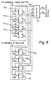
- Figure 4 ilfustrates an example of the control signal generator 16 in Figure 1.
- reference-numerals 16a and 16b denote voltage adjusting circuits which produce control signals for the 'variable phase shifter 10 and for the variable attenuator 12, respectively, and 16c denotes a decoder.
- the voltage adjusting circuit 16a has four potentiometers RV,, RV 2 , RV 3 and RV 4 and four electronic switches SW 1 , SW 2 , SW 3 , and SW 4 connected to sliding contacts of the respective potentiometers RV 1 , RV 2 , RV 3 , and RV 4 .
- a constant d.c To each of the potentiometers RV,, RV 2 , RV 3 , and RV 4 , a constant d.c.
- the decoder 16c receives the two-bit modulating signal via input terminals IN 7 and IN 8 and decodes it to produce one of four outputs. If the modulating signal is "11", the H level output appears only at the output terminal indicated by "11" to close the electronic switch SW 1 and also an electronic switch SW s .
- a voltage produced by the potentiometer RV 1 is applied to the variable phase shifter 10 as a control signal.
- a voltage produced by a potentiometer RV S is applied to the variable attenuator 12 as a control signal. Namely, in accordance with the modulating signal, one of the potentiometers RV,, RV 2 , RV 3 , and RV 4 is selected, and a voltage produced by the selected potentiometer is fed to the variable phase shifter 10. Similarly, one of potentiometers RV 5 , RV 6 , RV 7 , and RV 8 is selected in accordance with the modulating signal, and a voltage produced by the selected potentiometer is fed to the variable attenuator 12.
- Each of the potentiometers RV 1 to RV 8 is preliminarily adjusted to produce a voltage which can control the variable phase shifter 10 or the variable attenuator 12 to appropriately correct the phase or the amplitude of the carrier wave.
- the detail procedure for adjusting the potentiometer will be described later.
- FIGS 5 and 6 illustrate examples of the variable phase shifter 10 in Figure 1.
- a varactor diode D 7 is provided between an intermediate port of a circulator 34 and ground.
- the capacitance of the varactor diode D 7 varies with the d.c. voltage applied thereto from the control signal generator 16 ( Figure 1) via an input terminal IN 9 and a choke L 7 .
- the phase of the reflected carrier wave is shifted in accordance with the d.c. voltage (control signal) from the control signal generator 16.
- two varactor diodes D 8 and Dg are provided between terminals of a 90° hybrid 36 and ground.
- the capacitance of the varactor diodes D 8 and Dg varies with the d.c. voltage applied from the control signal generator 16 ( Figure 1) via an input terminal IN, o and chokes L 8 and Lg, respectively.
- the phase of the reflected carrier wave is shifted in accordance with the d.c. voltage (control signal) from the control signal generator 16.
- Figure 7 illustrates an example of the variable attenuator 12 shown in Figure 1.
- a diode D 10 such as a PIN-diode is provided in a transmission line.
- the impedance of the diode D 10 varies with the d.c. current (control signal) fed from the control signal generator 16 ( Figure 1) via an input terminal IN 11 and a choke L 10 .
- C 3 and C 4 denote capacitors for blocking the d.c. current.
- This adjustment is performed by adjusting the potentiometers VR 1 to VR 8 in the control signal generator 16 while maintaining the modulating signals at their respective values.
- the potentiometers RV 1 and RV S are adjusted while the modulating signal is maintained at "11" so that the phase position of the modulated wave from the quadrature phase modulator 14 becomes equal to a desired position, for instance, a position of 0°, and the amplitude of the modulated wave becomes equal to a desired value.
- the potentiometers RV 2 and RV 6 are similarly adjusted while the modulating signal is maintained at "10".
- the remaining potentiometers RV 3 and RV 7 and also RV 4 and RV a are adjusted in a like manner.
- variable phase shifter 10 compensates for the errors in the phase positions induced by the quadrature phase modulator 14, and the variable attenuator 12 compensates for deviation of the amplitude induced by the quadrature phase modulator 14. Therefore, the phase of the modulated wave outputted from the phase modulation system of Figure 1 is exactly controlled to the desired phase positions, i.e., 0°, 90°, 180°, and 270°, and the amplitude of the modulated wave is also exactly controlled to a constant value.
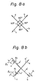
- Figure 8a indicates desired modulated waves a, b, c and d having a phase interval of 90° and an amplitude of a constant value.
- Figure 8b indicates an example of actual modulated wave modulated by the quadrature phase modulator without correcting the phase and the amplitude.
- solid lines a', b', c', and d' denote the actual modulated waves and broken lines a, b, c, and d denote the desired modulated waves.
- the actual modulated wave b' has a deviation I 1 of the amplitude with respect to the desired modulation wave b.
- the actual modulated wave c' has a deviation 1 2 of the amplitude and an error ⁇ 1 of the phase with respect to the desired modulated wave c.
- the actual modulated wave d' has a deviation 1 3 of the amplitude and an error ⁇ 2 of the phase with respect to the desired modulated wave d.
- the control signals from the control signal generator 16, that is, the potentiometers RV s to RV 3 are preliminarily adjusted depending upon the deviations I 1 , 1 2 , and 1 3 of the amplitude.
- these deviations, I 1 , 1 2 , and 1 3 at each phase position are compensated for by the variable attenuator 12.
- the errors ⁇ 1 and ⁇ 3 of the phase are compensated for by the variable phase shifter 10.
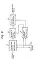
- FIG. 9 to 13 illustrate other embodiments of the present invention.
- variable phase shifter 10 and the variable attenuator 12 are connected to the output of the quadrature phase modulator 14, so as to correct the phase and the amplitude of the modulated wave from the modulator 14. Otherwise, the constitution of this embodiment is the same as that of the first embodiment.
- a third embodiment is shown in Figure 10.
- the variable attenuator 12 in the first embodiment of Figure 1 is omitted.
- This embodiment is effective if the quadrature phase modulator 14 can produce modulated waves having the same amplitude at each phase position.
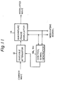
- a fourth embodiment is shown in Figure 11.
- the variable phase shifter 10 in the first embodiment of Figure 1 is omitted.
- the embodiment is used when the quadrature phase modulator 14 produces modulated waves with the phase positions exactly equal to the desired phase positions.
- variable phase shifter 10 or the variable attenuator 12. is connected to the output of the quadrature phase modulator 14 so as to correct the phase or the amplitude of the modulator wave from the modulator 14.
- the phase modulators are constituted by quadrature phase modulators so as to produce a modulated wave having four different phase positions.
- the phase modulators may be constituted by other multiple phase modulators so as to produce.a modulated wave having, for example, 8,16, or 32 different phase positions.
- variable phase shifter may be constituted by a current-controlled variable phase shifter
- variable attenuator may be constituted by a voltage-controlled variable attenuator.
- the control signals may be composed of voltage signals or current signals.
Landscapes
- Engineering & Computer Science (AREA)
- Computer Networks & Wireless Communication (AREA)
- Signal Processing (AREA)
- Digital Transmission Methods That Use Modulated Carrier Waves (AREA)
Description
- This invention relates to a phase modulation method and apparatus for use in a digital communication system.
- Multiple phase shift keying (MPSK) is a well known modulation system in which there are as many phase positions of a carrier wave as there are digital information input code elements. For example, with a quaternary code there are four different phase positions, ie. 0°, 90°, 180°, and 270° of the carrier wave. In such a modulation system it is required that the phase positions of the modulated waves be exactly equal to the desired phase positions and that the amplitude of the modulated waves in the different phase positions be maintained at a constant value.
- JP-A-56-60149 describes a known multiple phase shift keying system in which the modulated waves are fed to a high output amplifier. The problem which this system addresses is that the high output amplifier exhibits a non-linear response when operated in its saturation range and the system provides a pre-compensating circuit upstream of the signal modulator to adjust the amplitude of the carrier wave prior to the modulation step. The adjustment of amplitude is determined in accordance with the digital input signal which is also used to modulate the phase of the carrier wave.
- A paper entitled "The Use of TWT Amplifiers in M-ARY Amplitude and Phase Shift Keying Systems" published in IEEE, International Conference on Communications, 16th-18th June 1985, pages 36-17 to 36-21 describes a similar multiphase modulating transmitter to that described in the Japanese publication mentioned above. Once again, the problems of non-linearities in the output amplifier, in particular a TWT amplifier, are dealt with in a precompensating circuit.
- It has been found, however, that in addition to the problems of output amplifiers dealt with by the systems described above, the components in a phase modulator exhibit a difference in characteristics so that the phase positions of the modulated waves deviate from the desired phase positions. For example, in the case of a quadrature phase shift keying (QPSK) system, the phase differences of the modulated waves between neighbouring phase positions would not be equal to 90°. Furthermore, because of the differences in charactersitics of the components, the amplitude of the modulated waves in the different phase positions cannot be equally controlled.
- It is, therefore, an object of the present invention to provide a phase modulation method and apparatus whereby modulated waves can be easily obtained without error in the phase positions and/or deviation in amplitude.
- - According to a first aspect of the present invention, a method of generating a phase modulated wave in which the phase of a carrier wave is modulated in accordance with a binary modulating signal to produce the modulated wave is characterised by the step of correcting errors in the amplitude and/or phase of the modulated wave introduced during the modulation step by correcting the amplitude and/or the phase of the carrier wave or the modulated wave by predetermined amounts in response to the value of the binary modulating signal.
- According to a second aspect of the present invention, a method of generating a phase modulated wave in which the phase of a carrier wave is modulated in accordance with a binary modulating signal to produce the modulated wave, is characterised by the steps of producing, in response to the value of the binary modulating signal, at least one control signal; and correcting errors in the amplitude and/or phase of the modulated wave introduced during the modulation step by correcting, in accordance with the produced control signal or signals, the amplitude and/or the phase of the carrier wave or the modulated wave, whereby the phase position of the modulated waves becomes equal to one of a number of predetermined positions and the amplitudes of the'modulated waves coincide.
- According to a third aspect of the invention, phase modulation apparatus comprising modulator means for modulating the phase of a carrier wave in accordance with a binary modulating signal to produce a modulated wave; is characterised by means for producing, in response to the value of the binary modulating signal, at least one control signal; and means, coupled to the modulator means and to the control signal producing means, for correcting the amplitude and/ or the phase of the carrier wave or the modulated wave, in accordance with the control signal from the producing means in order to compensate for errors in the amplitude and/or phase of the modulated wave introduced by the modulator means, whereby the phase position of the modulated waves becomes equal to one of a number of predetermined positions and the amplitudes of the modulated waves are made to coincide.
- By use of the present invention, error in the phase position of modulated waves and/or deviation in the amplitude of the modulated waves due to the modulator means can be easily suppressed. That is, a phase modulation system with good modulation charactersitics can be obtained. Furthermore, a phase modulator having modulation characteristics can be used in this phase modulation system without deteriorating the modulation characteristics of the output from this system.
- Embodiments of the invention will now be described, by way of example, with reference to the accompanying drawings, in which:-
- Figure 1 is a block diagram of a first embodiment of the invention;
- Figures 2 and 3 are circuit diagrams of examples of different forms of quadrature phase modulator for use in the apparatus of Figure 1;
- Figure 4 is a circuit diagram of an example of a control signal generator for use in the apparatus of Figure 1;
- Figures 5 and 6 are circuit diagrams of examples of different forms of variable phase shifter for use in the apparatus of Figure 1;
- Figure 7 is a circuit diagram of an example of a variable attenuator for use in the apparatus of Figure 1;
- Figures 8a, 8b are diagrams for explaining error in the phase position of, and deviation of the amplitude of, modulated waves; and
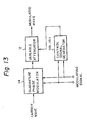
- Figures 9 to 13 are block diagrams of second to sixth embodiments of the present invention.
- Referring to Figure 1, which illustrates a first embodiment of the present invention, a phase modulation apparatus comprises a
variable phase shifter 10, avariable attenuator 12, aquadrature phase modulator 14 and acontrol signal generator 16. The variable phase shifter 10 shifts the phase of a carrier wave applied thereto in accordance with the voltage of a first control signal which is applied from thecontrol signal generator 16. Thevariable attenuator 12 controls the amplitude of the carrier wave from thevariable phase shifter 10 in accordance with the voltage of a second control signal which is applied from thecontrol signal generator 16. Thequadrature phase modulator 14 modulates the phase of the carrier wave from thevariable attenuator 12 in accordance with a modulating signal which is composed of a two-bit binary signal which is applied via input terminals IN1 and IN2. Therefore, in this embodiment, a modulated wave has one of four different phase positions, i.e. 0°, 90°, 180° and 270°, depending upon the modulating signal. Thecontrol signal generator 16 produces, in response to the modulating signal, the first and second control signals which control thevariable phase shifter 10 and thevariable attenuator 12, respectively. - Figures 2 and 3 illustrate examples of the
quadrature phase modulator 14 in Figure 1. - The quadrature phase modulator shown in Figure 2 is used in the microwave band and has two
circulators circulator 20 receives a carrier wave and thecirculator 22 outputs a modulated wave.Stubs circulators stubs stub 24 is equal to one-fourth of the carrier wavelength (λ/4) and the length of thestub 26 is equal to one- eighth of carrier wavelength (λ/8). Diodes D1 and D2, such as PIN-diodes, are provided on thestubs circulator 20 to return at the diode D1, and the phase of the carrier wave is not shifted. When the modulating signal applied to the input terminal IN3 is low (L) level, the diode D1 turns off and the phase of the carrier wave is shifted by 180°. Similarly to this, when the modulating signal applied to the input terminal IN4 is the H level, the phase of the carrier wave is not shifted, and when L level, the phase is shifted by 90°. Therefore, the phase of the carrier wave changes to four different phase positions of 0°, 90°, 180°, and 270° in response to the modulating signal. - However, since forward impedances of the diodes D1 and D2 are not perfectly zero during the on-state and are not perfectly infinity during the off-state and, furthermore, since there exist parasitic inductance and capacitance, phase positions of the wave modulated by a quadrature phase modulator as shown in Figure 2 have errors, and the amplitude of the modulated waves in the phase positions are not equal. Therefore, if a phase modulation system is constructed only by the quadrature phase modulator shown in Figure 2, the aforementioned problems of the prior art occur.
- The quadrature phase modulator shown in Figure 3 is used both in the microwave band and intermediate frequency band. In this modulator, a 90°
hybrid 30 receives a carrier wave and produces carrier waves having phase differences of 0° and 90° with respect to the received carrier. The outputs having phases of 0° and 90° from the 90°hybrid 30 are applied to primary windings of transformers T1 and T2, respectively. Diodes D3 and D4 are connected in series to a secondary winding of the transformer Ti, and diodes D5 and D6 are connected in series to a secondary winding of the transformer T2. Input terminals IN5 and IN6 are connected to mid-points of the secondary windings of the transformers T1 and T2, respectively. In Figure 3, furthermore, R1 and R2 denote dummy end resistors, C, and C2 denote capacitors, and Ls and L6 denote chokes. When the modulating signal applied to the input terminal IN5 is at H or L level, the diode D3 or D4 turns on. Therefore, the carrier wave having the phase of 0°, which was applied to the transformer Ti, is shifted by 0° or 180° in response to the modulating signal applied to the input terminal IN5. Also, when the modulating signal applied to the input terminal IN6 is at H or L level, the diode D5 or D6 turns on. Thus, the carrier wave having the phase of 90°, which was applied to the transformer T2, is shifted by 0° or 180° in response to the modulating signal. The above-mentioned shifted carrier waves from the transformers T1 and T2 are applied to a 0°hybrid 32 to output a modulated wave having one of the four different phase positions of 0°, 90°, 180°, and 270° depending upon the modulating signal. - However, since there are differences between outputs from each of the 90°
hybrid 30 and 0°hybrid 32, differences between the forward voltage drops of the diodes D3 to D6, and non- symmetry of the transformers T1 and T2, the phase positions of the waves modulated by the quadrature phase modulator shown in Figure 3 also have errors, and, furthermore, the amplitudes of the modulated waves in the phase positions are not equal to each other. That is, if a phase modulation system is constructed only by the quadrature phase modulator shown in Figure 3, the correct modulation charactersitics cannot be obtained as well as a system using only the quadrature phase modulator shown in Figure 2. - Figure 4 ilfustrates an example of the
control signal generator 16 in Figure 1. In Figure 4, reference-numerals variable phase shifter 10 and for thevariable attenuator 12, respectively, and 16c denotes a decoder. The voltage adjustingcircuit 16a has four potentiometers RV,, RV2, RV3 and RV4 and four electronic switches SW1, SW2, SW3, and SW4 connected to sliding contacts of the respective potentiometers RV1, RV2, RV3, and RV4. To each of the potentiometers RV,, RV2, RV3, and RV4, a constant d.c. voltage is supplied from respective voltage sources E1, E2, E3, and E4. Each of the electronic switches SW1, SW2, SW3, and SW4 is controlled by one of the outputs from thedecoder 16c. The othervoltage adjusting circuit 16b has the same constitution as the abovevoltage adjusting circuit 16a. Thedecoder 16c receives the two-bit modulating signal via input terminals IN7 and IN8 and decodes it to produce one of four outputs. If the modulating signal is "11", the H level output appears only at the output terminal indicated by "11" to close the electronic switch SW1 and also an electronic switch SWs. Thus, in this case, a voltage produced by the potentiometer RV1 is applied to thevariable phase shifter 10 as a control signal. Also, a voltage produced by a potentiometer RVS is applied to thevariable attenuator 12 as a control signal. Namely, in accordance with the modulating signal, one of the potentiometers RV,, RV2, RV3, and RV4 is selected, and a voltage produced by the selected potentiometer is fed to thevariable phase shifter 10. Similarly, one of potentiometers RV5, RV6, RV7, and RV8 is selected in accordance with the modulating signal, and a voltage produced by the selected potentiometer is fed to thevariable attenuator 12. Each of the potentiometers RV1 to RV8 is preliminarily adjusted to produce a voltage which can control thevariable phase shifter 10 or thevariable attenuator 12 to appropriately correct the phase or the amplitude of the carrier wave. The detail procedure for adjusting the potentiometer will be described later. - Figures 5 and 6 illustrate examples of the
variable phase shifter 10 in Figure 1. - In the phase shifter shown in Figure 5, a varactor diode D7 is provided between an intermediate port of a
circulator 34 and ground. The capacitance of the varactor diode D7 varies with the d.c. voltage applied thereto from the control signal generator 16 (Figure 1) via an input terminal IN9 and a choke L7. Thus, the phase of the reflected carrier wave is shifted in accordance with the d.c. voltage (control signal) from thecontrol signal generator 16. - In the phase shifter shown in Figure 6, two varactor diodes D8 and Dg are provided between terminals of a 90°
hybrid 36 and ground. The capacitance of the varactor diodes D8 and Dg varies with the d.c. voltage applied from the control signal generator 16 (Figure 1) via an input terminal IN,o and chokes L8 and Lg, respectively. Thus, the phase of the reflected carrier wave is shifted in accordance with the d.c. voltage (control signal) from thecontrol signal generator 16. - Figure 7 illustrates an example of the
variable attenuator 12 shown in Figure 1. A diode D10 such as a PIN-diode is provided in a transmission line. The impedance of the diode D10 varies with the d.c. current (control signal) fed from the control signal generator 16 (Figure 1) via an input terminal IN11 and a choke L10. In Figure 7, C3 and C4 denote capacitors for blocking the d.c. current. - The operation of the above-mentioned embodiment will now be described.
- Before operating the phase modulation system, it is necessary to adjust the control signals. This adjustment is performed by adjusting the potentiometers VR1 to VR8 in the
control signal generator 16 while maintaining the modulating signals at their respective values. For example, the potentiometers RV1 and RVS are adjusted while the modulating signal is maintained at "11" so that the phase position of the modulated wave from thequadrature phase modulator 14 becomes equal to a desired position, for instance, a position of 0°, and the amplitude of the modulated wave becomes equal to a desired value. The potentiometers RV2 and RV6 are similarly adjusted while the modulating signal is maintained at "10". The remaining potentiometers RV3 and RV7 and also RV4 and RVa are adjusted in a like manner. - As a result of the above-adjustment, during operation, the
variable phase shifter 10 compensates for the errors in the phase positions induced by thequadrature phase modulator 14, and thevariable attenuator 12 compensates for deviation of the amplitude induced by thequadrature phase modulator 14. Therefore, the phase of the modulated wave outputted from the phase modulation system of Figure 1 is exactly controlled to the desired phase positions, i.e., 0°, 90°, 180°, and 270°, and the amplitude of the modulated wave is also exactly controlled to a constant value. - Figure 8a indicates desired modulated waves a, b, c and d having a phase interval of 90° and an amplitude of a constant value. On the other hand, Figure 8b indicates an example of actual modulated wave modulated by the quadrature phase modulator without correcting the phase and the amplitude. In Figure 8b, solid lines a', b', c', and d' denote the actual modulated waves and broken lines a, b, c, and d denote the desired modulated waves. The actual modulated wave b' has a deviation I1 of the amplitude with respect to the desired modulation wave b. The actual modulated wave c' has a deviation 12 of the amplitude and an error θ1 of the phase with respect to the desired modulated wave c. The actual modulated wave d' has a deviation 13 of the amplitude and an error θ2 of the phase with respect to the desired modulated wave d. The control signals from the
control signal generator 16, that is, the potentiometers RVs to RV3, are preliminarily adjusted depending upon the deviations I1, 12, and 13 of the amplitude. Thus these deviations, I1, 12, and 13 at each phase position are compensated for by thevariable attenuator 12. In a like manner, the errors θ1 and θ3 of the phase are compensated for by thevariable phase shifter 10. - Figures 9 to 13 illustrate other embodiments of the present invention.
- A second embodiment is shown in Figure 9, wherein the
variable phase shifter 10 and thevariable attenuator 12 are connected to the output of thequadrature phase modulator 14, so as to correct the phase and the amplitude of the modulated wave from themodulator 14. Otherwise, the constitution of this embodiment is the same as that of the first embodiment. - A third embodiment is shown in Figure 10. In this embodiment, the
variable attenuator 12 in the first embodiment of Figure 1 is omitted. This embodiment is effective if thequadrature phase modulator 14 can produce modulated waves having the same amplitude at each phase position. - A fourth embodiment is shown in Figure 11. In this embodiment, the
variable phase shifter 10 in the first embodiment of Figure 1 is omitted. The embodiment is used when thequadrature phase modulator 14 produces modulated waves with the phase positions exactly equal to the desired phase positions. - In the fifth and sixth embodiments shown in Figures 12 and 13, the
variable phase shifter 10 or thevariable attenuator 12. is connected to the output of thequadrature phase modulator 14 so as to correct the phase or the amplitude of the modulator wave from themodulator 14. - In the above-mentioned embodiments, the phase modulators are constituted by quadrature phase modulators so as to produce a modulated wave having four different phase positions. However, according to the present invention, the phase modulators may be constituted by other multiple phase modulators so as to produce.a modulated wave having, for example, 8,16, or 32 different phase positions.
- According to the present invention, furthermore, the variable phase shifter may be constituted by a current-controlled variable phase shifter, and the variable attenuator may be constituted by a voltage-controlled variable attenuator. The control signals, of course, may be composed of voltage signals or current signals.
Claims (15)
Applications Claiming Priority (2)
| Application Number | Priority Date | Filing Date | Title |
|---|---|---|---|
| JP57190398A JPS5985166A (en) | 1982-10-29 | 1982-10-29 | Phase modulator |
| JP190398/82 | 1982-10-29 |
Publications (3)
| Publication Number | Publication Date |
|---|---|
| EP0107980A2 EP0107980A2 (en) | 1984-05-09 |
| EP0107980A3 EP0107980A3 (en) | 1986-03-05 |
| EP0107980B1 true EP0107980B1 (en) | 1989-01-18 |
Family
ID=16257486
Family Applications (1)
| Application Number | Title | Priority Date | Filing Date |
|---|---|---|---|
| EP83306598A Expired EP0107980B1 (en) | 1982-10-29 | 1983-10-28 | Phase modulation method and apparatus |
Country Status (4)
| Country | Link |
|---|---|
| US (1) | US4565980A (en) |
| EP (1) | EP0107980B1 (en) |
| JP (1) | JPS5985166A (en) |
| DE (1) | DE3379019D1 (en) |
Families Citing this family (16)
| Publication number | Priority date | Publication date | Assignee | Title |
|---|---|---|---|---|
| SE459774B (en) * | 1987-11-27 | 1989-07-31 | Ericsson Telefon Ab L M | DEVICE FOR COMPENSATION OF ERRORS APPLICABLE IN A SQUARE MODULATOR |
| JPH0771118B2 (en) * | 1989-12-27 | 1995-07-31 | 三菱電機株式会社 | Modulator |
| US4968908A (en) * | 1989-03-06 | 1990-11-06 | The United States Of America As Represented By The Secretary Of Commerce | Method and apparatus for wide band phase modulation |
| EP0431201B1 (en) * | 1989-06-30 | 1995-12-13 | Nippon Telegraph And Telephone Corporation | Linear transmitter |
| US4993047A (en) * | 1989-09-05 | 1991-02-12 | At&T Bell Laboratories | Volterra linearizer for digital transmission |
| GB2239142A (en) * | 1989-12-15 | 1991-06-19 | Philips Electronic Associated | Variable bi-phase modulator circuits and variable resistors |
| SE465494B (en) * | 1990-01-22 | 1991-09-16 | Ericsson Telefon Ab L M | PROCEDURE TO COMPENSATE FOR OILARITIES IN A FINAL AMPLIFIER |
| JP2690168B2 (en) * | 1990-04-23 | 1997-12-10 | 沖電気工業株式会社 | Distortion correction device for power amplifier |
| NO944905L (en) * | 1993-12-21 | 1995-06-22 | Nec Corp | Transmitting device for mobile satellite communication equipment |
| US5455543A (en) * | 1994-01-28 | 1995-10-03 | Thomson Consumer Electronics, Inc. | Low power consumption binary phase shift keyed (BPSK) modulator using absorptive electronic switching techniques |
| EP0783797B1 (en) * | 1995-07-21 | 2003-11-05 | Koninklijke Philips Electronics N.V. | A wireless digital communication device, and a pulse shaping network |
| GB2334187A (en) * | 1998-02-04 | 1999-08-11 | Motorola Ltd | Quadrature modulator with automatic compensation |
| US6889086B2 (en) * | 2001-04-06 | 2005-05-03 | Cardiac Pacemakers, Inc. | Passive telemetry system for implantable medical device |
| US7020070B2 (en) | 2001-04-10 | 2006-03-28 | Telefonaktiebolaget L M Ericsson (Publ) | Selectively controlled modulation distortion of an IQ-baseband signal |
| US7042936B2 (en) * | 2002-04-18 | 2006-05-09 | The Boeing Company | Dynamic amplitude tilt equalizer |
| JP5180091B2 (en) * | 2005-11-24 | 2013-04-10 | テクニシェ・ウニフェルシテイト・デルフト | Varactor element and low distortion varactor circuit device |
Family Cites Families (7)
| Publication number | Priority date | Publication date | Assignee | Title |
|---|---|---|---|---|
| US3378637A (en) * | 1963-06-17 | 1968-04-16 | Kokusai Denshin Denwa Co Ltd | System for generating single sideband phase modulated telegraphic signals |
| US3437957A (en) * | 1966-06-28 | 1969-04-08 | Us Air Force | Microwave phase shift modulator for use with tunnel diode switching circuits |
| US3437958A (en) * | 1966-09-27 | 1969-04-08 | Bell Telephone Labor Inc | Phase modulator including a driver and a driven oscillator |
| DE1289140C2 (en) * | 1967-08-21 | 1976-08-12 | Siemens AG, 1000 Berlin und 8000 München | AMPLIFIER WITH A RUNNING TUBE, IN PARTICULAR WALKING FIELD TUBE |
| JPS5038488B1 (en) * | 1970-08-14 | 1975-12-10 | ||
| US4130811A (en) * | 1977-12-27 | 1978-12-19 | Hughes Aircraft Company | Modulation system |
| JPS5928306B2 (en) * | 1978-11-29 | 1984-07-12 | 三菱電機株式会社 | phase modulator |
-
1982
- 1982-10-29 JP JP57190398A patent/JPS5985166A/en active Pending
-
1983
- 1983-10-26 US US06/545,460 patent/US4565980A/en not_active Expired - Fee Related
- 1983-10-28 EP EP83306598A patent/EP0107980B1/en not_active Expired
- 1983-10-28 DE DE8383306598T patent/DE3379019D1/en not_active Expired
Also Published As
| Publication number | Publication date |
|---|---|
| US4565980A (en) | 1986-01-21 |
| EP0107980A3 (en) | 1986-03-05 |
| DE3379019D1 (en) | 1989-02-23 |
| JPS5985166A (en) | 1984-05-17 |
| EP0107980A2 (en) | 1984-05-09 |
Similar Documents
| Publication | Publication Date | Title |
|---|---|---|
| US4565980A (en) | PSK Modulator with preset amplitude and phase corrections for each phase | |
| US5852389A (en) | Direct QAM modulator | |
| AU770637B2 (en) | A radio transceiver and a method of preventing transmission spurious response | |
| EP0360178B1 (en) | Transmitter circuit for efficiently transmitting communication traffic via phase modulated carrier signals | |
| EP1119905B1 (en) | In-line, unbalanced amplifier, pre-distortion circuit | |
| US5144258A (en) | Power amplifier system for radio transmitter and method for using the same | |
| JP3169803B2 (en) | Nonlinear compensation circuit of power amplifier | |
| US6741139B2 (en) | Optical to microwave converter using direct modulation phase shift keying | |
| EP0689322A1 (en) | Tunable BPSK modulator | |
| US4588958A (en) | Adjustable reflective predistortion circuit | |
| WO2000038388A1 (en) | Qam modulator for radio communications | |
| US7248639B2 (en) | Method for reducing the out-of-band emission in AM transmitters for digital transmission | |
| EP0828385B1 (en) | Digital amplitude modulation amplifier and television broadcasting machine | |
| US4633197A (en) | Single resonant tank modulated oscillator | |
| EP0570979B1 (en) | Quadrature modulation circuit | |
| US4593410A (en) | Single-sideband transmitter and method for operating this transmitter | |
| EP0518835B1 (en) | Method of compensating the dependence of the useful transmitter signal on the transfer function of a combiner filter | |
| CA1182875A (en) | Spectrum shaping microwave digital modulators | |
| EP0953232B1 (en) | Linearization arrangement of a power amplifier | |
| US4794458A (en) | Modulation device | |
| US3946337A (en) | Phase modulator for phase shift key communications systems | |
| EP0570125B1 (en) | Unbalanced-balanced converter as a mixer input circuit | |
| US4575858A (en) | PSK modulation by temporarily increasing frequency to achieve phase change | |
| KR20140145609A (en) | Apparatus for generating dedicated data channels in inductive coupled rfid | |
| US3967217A (en) | Modulator for digital microwave transmitter |
Legal Events
| Date | Code | Title | Description |
|---|---|---|---|
| PUAI | Public reference made under article 153(3) epc to a published international application that has entered the european phase |
Free format text: ORIGINAL CODE: 0009012 |
|
| AK | Designated contracting states |
Designated state(s): DE FR GB IT NL |
|
| PUAL | Search report despatched |
Free format text: ORIGINAL CODE: 0009013 |
|
| AK | Designated contracting states |
Kind code of ref document: A3 Designated state(s): DE FR GB IT NL |
|
| 17P | Request for examination filed |
Effective date: 19860819 |
|
| 17Q | First examination report despatched |
Effective date: 19870807 |
|
| GRAA | (expected) grant |
Free format text: ORIGINAL CODE: 0009210 |
|
| AK | Designated contracting states |
Kind code of ref document: B1 Designated state(s): DE FR GB IT NL |
|
| REF | Corresponds to: |
Ref document number: 3379019 Country of ref document: DE Date of ref document: 19890223 |
|
| ET | Fr: translation filed | ||
| ITF | It: translation for a ep patent filed | ||
| PLBE | No opposition filed within time limit |
Free format text: ORIGINAL CODE: 0009261 |
|
| STAA | Information on the status of an ep patent application or granted ep patent |
Free format text: STATUS: NO OPPOSITION FILED WITHIN TIME LIMIT |
|
| 26N | No opposition filed | ||
| ITTA | It: last paid annual fee | ||
| PGFP | Annual fee paid to national office [announced via postgrant information from national office to epo] |
Ref country code: NL Payment date: 19941031 Year of fee payment: 12 |
|
| PGFP | Annual fee paid to national office [announced via postgrant information from national office to epo] |
Ref country code: FR Payment date: 19951010 Year of fee payment: 13 |
|
| PGFP | Annual fee paid to national office [announced via postgrant information from national office to epo] |
Ref country code: GB Payment date: 19951019 Year of fee payment: 13 |
|
| PGFP | Annual fee paid to national office [announced via postgrant information from national office to epo] |
Ref country code: DE Payment date: 19951026 Year of fee payment: 13 |
|
| PG25 | Lapsed in a contracting state [announced via postgrant information from national office to epo] |
Ref country code: NL Effective date: 19960501 |
|
| NLV4 | Nl: lapsed or anulled due to non-payment of the annual fee |
Effective date: 19960501 |
|
| PG25 | Lapsed in a contracting state [announced via postgrant information from national office to epo] |
Ref country code: GB Effective date: 19961028 |
|
| GBPC | Gb: european patent ceased through non-payment of renewal fee |
Effective date: 19961028 |
|
| PG25 | Lapsed in a contracting state [announced via postgrant information from national office to epo] |
Ref country code: FR Effective date: 19970630 |
|
| PG25 | Lapsed in a contracting state [announced via postgrant information from national office to epo] |
Ref country code: DE Effective date: 19970701 |
|
| REG | Reference to a national code |
Ref country code: FR Ref legal event code: ST |