EP0105695B1 - Mos/bipolar integrated circuit device and manufacturing method thereof - Google Patents
Mos/bipolar integrated circuit device and manufacturing method thereof Download PDFInfo
- Publication number
- EP0105695B1 EP0105695B1 EP83305767A EP83305767A EP0105695B1 EP 0105695 B1 EP0105695 B1 EP 0105695B1 EP 83305767 A EP83305767 A EP 83305767A EP 83305767 A EP83305767 A EP 83305767A EP 0105695 B1 EP0105695 B1 EP 0105695B1
- Authority
- EP
- European Patent Office
- Prior art keywords
- transistors
- field effect
- layer
- bipolar transistors
- insulating layer
- Prior art date
- Legal status (The legal status is an assumption and is not a legal conclusion. Google has not performed a legal analysis and makes no representation as to the accuracy of the status listed.)
- Expired
Links
- 238000004519 manufacturing process Methods 0.000 title claims description 12
- 239000004065 semiconductor Substances 0.000 claims description 47
- 239000000758 substrate Substances 0.000 claims description 36
- 229910021420 polycrystalline silicon Inorganic materials 0.000 claims description 28
- 230000005669 field effect Effects 0.000 claims description 26
- 229910044991 metal oxide Inorganic materials 0.000 claims description 13
- 150000004706 metal oxides Chemical class 0.000 claims description 13
- 229910021419 crystalline silicon Inorganic materials 0.000 claims description 11
- 239000012535 impurity Substances 0.000 claims description 11
- 150000002500 ions Chemical class 0.000 claims description 11
- 238000000034 method Methods 0.000 claims description 9
- 238000000137 annealing Methods 0.000 claims description 8
- VYPSYNLAJGMNEJ-UHFFFAOYSA-N Silicium dioxide Chemical compound O=[Si]=O VYPSYNLAJGMNEJ-UHFFFAOYSA-N 0.000 claims description 4
- 239000000463 material Substances 0.000 claims description 3
- 238000001953 recrystallisation Methods 0.000 claims description 3
- 238000000059 patterning Methods 0.000 claims description 2
- 238000000151 deposition Methods 0.000 claims 1
- 229910052814 silicon oxide Inorganic materials 0.000 claims 1
- 239000010408 film Substances 0.000 description 35
- 239000010410 layer Substances 0.000 description 29
- 230000015572 biosynthetic process Effects 0.000 description 6
- 230000001133 acceleration Effects 0.000 description 4
- 238000009413 insulation Methods 0.000 description 4
- 238000012856 packing Methods 0.000 description 4
- 230000002411 adverse Effects 0.000 description 3
- 229910052796 boron Inorganic materials 0.000 description 3
- 238000002347 injection Methods 0.000 description 3
- 239000007924 injection Substances 0.000 description 3
- 108010053481 Antifreeze Proteins Proteins 0.000 description 2
- XUIMIQQOPSSXEZ-UHFFFAOYSA-N Silicon Chemical compound [Si] XUIMIQQOPSSXEZ-UHFFFAOYSA-N 0.000 description 2
- XKRFYHLGVUSROY-UHFFFAOYSA-N argon Substances [Ar] XKRFYHLGVUSROY-UHFFFAOYSA-N 0.000 description 2
- 229910052786 argon Inorganic materials 0.000 description 2
- -1 boron ions Chemical class 0.000 description 2
- 230000003247 decreasing effect Effects 0.000 description 2
- 238000010894 electron beam technology Methods 0.000 description 2
- BASFCYQUMIYNBI-UHFFFAOYSA-N platinum Chemical compound [Pt] BASFCYQUMIYNBI-UHFFFAOYSA-N 0.000 description 2
- 229910052710 silicon Inorganic materials 0.000 description 2
- 239000010703 silicon Substances 0.000 description 2
- SYQQWGGBOQFINV-FBWHQHKGSA-N 4-[2-[(2s,8s,9s,10r,13r,14s,17r)-10,13-dimethyl-17-[(2r)-6-methylheptan-2-yl]-3-oxo-1,2,6,7,8,9,11,12,14,15,16,17-dodecahydrocyclopenta[a]phenanthren-2-yl]ethoxy]-4-oxobutanoic acid Chemical compound C1CC2=CC(=O)[C@H](CCOC(=O)CCC(O)=O)C[C@]2(C)[C@@H]2[C@@H]1[C@@H]1CC[C@H]([C@H](C)CCCC(C)C)[C@@]1(C)CC2 SYQQWGGBOQFINV-FBWHQHKGSA-N 0.000 description 1
- ZOXJGFHDIHLPTG-UHFFFAOYSA-N Boron Chemical compound [B] ZOXJGFHDIHLPTG-UHFFFAOYSA-N 0.000 description 1
- OAICVXFJPJFONN-UHFFFAOYSA-N Phosphorus Chemical compound [P] OAICVXFJPJFONN-UHFFFAOYSA-N 0.000 description 1
- 229910052782 aluminium Inorganic materials 0.000 description 1
- XAGFODPZIPBFFR-UHFFFAOYSA-N aluminium Chemical compound [Al] XAGFODPZIPBFFR-UHFFFAOYSA-N 0.000 description 1
- 229910052785 arsenic Inorganic materials 0.000 description 1
- RQNWIZPPADIBDY-UHFFFAOYSA-N arsenic atom Chemical compound [As] RQNWIZPPADIBDY-UHFFFAOYSA-N 0.000 description 1
- 230000005540 biological transmission Effects 0.000 description 1
- 230000015556 catabolic process Effects 0.000 description 1
- 238000005229 chemical vapour deposition Methods 0.000 description 1
- 238000006731 degradation reaction Methods 0.000 description 1
- 230000000593 degrading effect Effects 0.000 description 1
- 238000010586 diagram Methods 0.000 description 1
- 238000009792 diffusion process Methods 0.000 description 1
- 238000009826 distribution Methods 0.000 description 1
- 230000000694 effects Effects 0.000 description 1
- 238000002003 electron diffraction Methods 0.000 description 1
- 238000005530 etching Methods 0.000 description 1
- 230000017525 heat dissipation Effects 0.000 description 1
- 238000005224 laser annealing Methods 0.000 description 1
- 229910021421 monocrystalline silicon Inorganic materials 0.000 description 1
- 229910052698 phosphorus Inorganic materials 0.000 description 1
- 239000011574 phosphorus Substances 0.000 description 1
- 229910052697 platinum Inorganic materials 0.000 description 1
- 230000002035 prolonged effect Effects 0.000 description 1
- 239000002210 silicon-based material Substances 0.000 description 1
- 239000002344 surface layer Substances 0.000 description 1
- 239000010409 thin film Substances 0.000 description 1
Images


Classifications
-
- H—ELECTRICITY
- H10—SEMICONDUCTOR DEVICES; ELECTRIC SOLID-STATE DEVICES NOT OTHERWISE PROVIDED FOR
- H10D—INORGANIC ELECTRIC SEMICONDUCTOR DEVICES
- H10D88/00—Three-dimensional [3D] integrated devices
-
- H—ELECTRICITY
- H10—SEMICONDUCTOR DEVICES; ELECTRIC SOLID-STATE DEVICES NOT OTHERWISE PROVIDED FOR
- H10D—INORGANIC ELECTRIC SEMICONDUCTOR DEVICES
- H10D84/00—Integrated devices formed in or on semiconductor substrates that comprise only semiconducting layers, e.g. on Si wafers or on GaAs-on-Si wafers
- H10D84/01—Manufacture or treatment
- H10D84/0107—Integrating at least one component covered by H10D12/00 or H10D30/00 with at least one component covered by H10D8/00, H10D10/00 or H10D18/00, e.g. integrating IGFETs with BJTs
- H10D84/0109—Integrating at least one component covered by H10D12/00 or H10D30/00 with at least one component covered by H10D8/00, H10D10/00 or H10D18/00, e.g. integrating IGFETs with BJTs the at least one component covered by H10D12/00 or H10D30/00 being a MOS device
-
- H—ELECTRICITY
- H10—SEMICONDUCTOR DEVICES; ELECTRIC SOLID-STATE DEVICES NOT OTHERWISE PROVIDED FOR
- H10D—INORGANIC ELECTRIC SEMICONDUCTOR DEVICES
- H10D84/00—Integrated devices formed in or on semiconductor substrates that comprise only semiconducting layers, e.g. on Si wafers or on GaAs-on-Si wafers
- H10D84/01—Manufacture or treatment
- H10D84/02—Manufacture or treatment characterised by using material-based technologies
- H10D84/03—Manufacture or treatment characterised by using material-based technologies using Group IV technology, e.g. silicon technology or silicon-carbide [SiC] technology
- H10D84/038—Manufacture or treatment characterised by using material-based technologies using Group IV technology, e.g. silicon technology or silicon-carbide [SiC] technology using silicon technology, e.g. SiGe
Definitions
- the present invention relates generally to an integrated semiconductor device and, more particularly, to a MOS/bipolar semiconductor device having different transistor elements, such as unipolar transistors including metal oxide semiconductor field effect transistors (MOSFETs) and bipolar transistors (e.g., junction transistors), on the same substrate, and to a manufacturing method thereof.
- MOSFETs metal oxide semiconductor field effect transistors
- bipolar transistors e.g., junction transistors
- MOS transistors and bipolar transistors are used as control signal sources, while bipolar transistors are used as elements through which the high currents to be controlled flow.
- an output control signal from the MOS transistor is supplied to the base of the bipolar transistor.
- MOS and bipolar transistors ⁇ are two-dimensionally formed on a major surface of the same semiconductor substrate. In this case, three problems are presented:
- JP-A-5793562 discloses a semiconductor device in which a MOS FET is stacked above a bipolar transistor formed in the substrate.
- an integrated circuit (lC) device including unipolar transistors, such as metal oxide semiconductor field effect transistors (MOSFETs), and bipolar transistors, such as junction transistors, according to the present invention
- MOSFETs metal oxide semiconductor field effect transistors
- bipolar transistors such as junction transistors
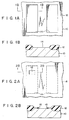
- An insulating layer or field insulation layer 12 having rectangular windows 14 is formed on an n-type single crystalline semiconductor substrate 10 containing, e.g., phosphorus as an impurity, in a concentration of 1.5 x 10 11 cm- 3 , as shown in Fig. 1A.
- the windows 14 correspond to element formation regions of MOS transistors such as enhancement-type MOS transistors.
- Fig. 1B illustrates a sectional view of the structure of Fig. 1A taken along the line 1B-1B thereof. It should be noted that these drawings are not drawn to scale.
- Fig. 1 is exposed in a dry atmosphere at a predetermined temperature (i.e., at a high temperature of 900°C), to deposit a gate oxide film 16 thereon to a thickness of about 50nm (500 A), as shown in Figs. 2A and 2B.
- a rectangular opening 18 corresponding to a contact hole of the drain region of an MOS transistor is formed within each element formation region 14.
- P-type impurity ions such as boron ions are injected into the substrate 10 through the opening 18, at a dose of 4 x 1015 cm- 2 and an ion acceleration voltage of 40 keV, thereby decreasing the resistance of the drain region of the substrate.
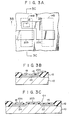
- the polycrystalline silicon film 20 is patterned, as shown in Figs. 3A to 3C, thereby obtaining patterned films 20a and 20b.
- the patterend polycrystalline silicon film 20a contacts the drain region of one MOS transistor formation region 14a through the contact hole 18 and also serves as the gate region of another MOS transistor to be formed in another MOS transistor formation region 14b. It should be noted that the self-alignment technique among silicon gate techniques is utilized to pattern the polycrystalline silicon film 20.
- an etchant used for patterning the film 20 stops its etching action when the etchant reaches the gate oxide film 16 or the field insulation layer 12.
- a p-type impurity such as boron is injected under the same conditions as previously described, thereby forming two p-type high- impurity regions 22 and 24 in a surface layer of the substrate 10 within each of the MOS transistor formation regions 14.
- the respective high- impurity regions 22 and 24 correspond to the source and drain, respectively, of an MOS transistor.
- a p-channel MOS transistor Q1 is prepared. It should be noted that boron ions are injected into the patterned polycrystalline films 20a and 20b as well as into the source and drain regions 22 and 24 within the substrate 10, in accordance with ion injection for forming the source and drain regions.
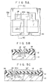
- an insulating film 26 such as a plasma CVD-Si0 2 film is deposited to cover the entire surface of the structure shown in Fig. 4, to a thickness of, e.g., about 600nm (6,000 A).
- An opening 28 serving as another contact hole or drain contact hole is formed in a portion of the film 26 corresponding to the contact hole 18 of the MOS drain region.
- a second polycrystalline silicon film 30 having a thickness of 300 nm (3,000 A) is deposited to cover the entire surface of the film 26 having the drain contact hole 28. Therefore, the second polycrystalline silicon film 30 contacts the underlying first polycrystalline silicon film 20a through the drain contact hole 28.
- the polycrystalline silicon material on the drain region 24 of the MOS transistor Q1 at the position of the contact hole 18 has a total thickness of 600nm (6,OOOA), corresponding to the sum of the thicknesses of the first and second polycrystalline layers 20a and 30.
- the MOS drain region 24 is electrically connected to the second polycrystalline silicon film 30 through the two contact holes, 18, 28 and the first polycrystalline silicon film 20a.
- the second polycrystalline silicon film 30 is recrystallized by a rapid annealing technique, such as a laser beam annealing technique, so that the second polycrystalline silicon film 30 is converted to a single-crystalline silicon.
- a rapid annealing technique such as a laser beam annealing technique
- a CW-argon laser was used as an annealing beam source
- the raster scan rate was 9.8 cm/sec
- the raster scan pitch was set at from 5 to 20 ⁇ m.
- the atmosphere temperature during annealing was kept at a temperature of 490°C, and the laser power was 7 to 15 W.
- laser annealing was performed under these conditions, it was found that the second polycrystalline silicon film 30 was effectively recrystallized by using the film portion 30a at the drain contact hole 28 as a seed.
- a suitable laser beam power was in the range between 7 W and 15 W.
- the laser power exceeded this range, the second polycrystalline silicon film 30 was melted.
- the laser power was below this range, the polycrystalline silicon film was not recrystallized.
- the polycrystalline silicon film 30 was sufficiently recrystallized in the laser power range between 7 W and 15 W.
- Kikuchi lines were clearly observed.
- the recrystallized film was observed by electron beam transmission, only a very small amount of polycrystalline silicon was observed.
- the polycrystalline silicon film 30 was substantially completely recrystallized to single-crystalline silicon.
- the recrystallized monocrystalline silicon film 30' is then patterned, as shown in Figs. 5A to 5C. Therefore, single-crystalline substrate layers 30'-1 and 30'-2 are prepared for forming bipolar transistors therein, respectively, above the MOS transistors.
- bipolar transistors are formed in the layers 30-1 and 30-2, respectively.
- arsenic is injected into each of the layers 30'-1 and 30'-2, using a known ion injection mask (not shown).
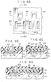
- an npn bipolar transistor Q2 having a first n-conductivity type region (emitter region) 32, a p-conductivity type region 34 (base region) 34 and a second n-conductivity type region (collector region) 36 is formed in the layer 30'-1.
- a bipolar transistor is formed in the layer 30'-2, in the same manner as that formed in the layer 30'-1.
- the ion injection conditions for forming the pnp junction structure were given as follows: a dose of 1 x 10 16 cm- 2 and an ion acceleration voltage of 30 keV at the bipolar transistor emitter region; a dose of 1 x 1011 cm- 2 and an ion acceleration voltage of 50 keV at the collector region; and a dose of 1 x 10 16 cm- 2 and an ion acceleration voltage of 50 keV at a portion adjoining a conductive layer (not shown) serving as the collector electrode.
- an insulating film 38 made of a CVD-Si0 2 film is deposited to cover the entire surface of the structure.
- Contact holes 40a, 40b, 40c for the base, emitter and collector electrodes, respectively, are formed in the film 38.
- Wiring pattern layers (not shown) made of aluminum or platinum are deposited to cover the resultant structure and are patterned, thereby obtaining a desired configuration of circuit cbnnections.
- Fig. 7 illustrates an equivalent circuit of a pair of a MOS and a bipolar transistor stacked in a two-storied structure in the semiconductor IC device manufactured as described above.
- the drain 24 of the underlying MOS transistor Q1 is connected to the collector region 36 of the overlying bipolar transistor Q2 and to a power supply terminal 42, through an equivalent resistor component R1 (including a junction resistance between the layer); and to the base region 34 of the bipolar transistor Q2, through another resistor component R2.
- a voltage V DD is supplied to the power supply terminal 42.
- the resistance R1 between the power supply terminal 42 and the MOS drain 24 was measured to be 7.1 kQ
- the resistance R2 between the MOS drain 24 and the bipolar base 34 was measured to be 10 k ⁇ . Under such conditions, the ON resistance of the MOS transistor Q1 was 42.9 kQ.
- a base-emitter voltage V BE is plotted along the axis of the abscissa, and a collector current density J c is plotted along the axis of the ordinate.
- a collector-emitter voltage V CE is preset to be 5.0 V.
- the bipolar transistor has good electrical characteristics.
- the lifetime of the electrons in the base was measured in accordance with these electrical characteristics, it was found to be 10- 6 sec. This lifetime was substantially the same as that of a transistor formed on a conventional bulk substrate.
- the dynamic characteristics of the semiconductor IC device of the described embodiment may be described as follows.
- the power supply voltage V DD was -5 V, and a voltage which was -1.0 V higher than a threshold voltage was applied to the gate of the MOS transistor Q1, so that the MOS transistor Q1 was rendered conductive.
- the potential (i.e., the drain potential) at a node 44 shown in Fig. 7 was measured by calculating the ratio of resistance R1 to the ON resistance of the MOS transistor Q1, and was found to be -4.29 V.
- the potential at the base was -4.3 V, since the resistance R2 was present between the MOS drain 24 and the bipolar base 34.
- the base current was not more than 10- 6 A/cm 2
- the MOS transistor was rendered nonconductive, the potential at the MOS drain was -4.9 V, the potential at the bipolar base was the same as that of the MOS drain, the base current was not more than 10- 11 A/cm 2 , and the collector current J c was 10- 11 A/cm 2 .
- the collector current J c of the bipolar transistor varied in the range between 10- 4 A/cm 2 , to 10- 11 A/ cm 2 . In other words, it was found that good switching characteristics could be obtained.
- the bipolar transistors Q2 were stereographically (in a two-storied structure) stacked above the MOS transistors Q1 formed on the substrate 10, through the insulating layer. Therefore, the packing density of the circuit with respect to the substrate 10 can be greatly increased. In the device described, it was confirmed by the present inventors that the element area of the substrate could be decreased by about 55%, as compared to that of the conventional two-dimensional IC device having both MOS and bipolar transistors.
- the MOS transistors can be simultaneously formed on the substrate 10 in the first step. Thereafter, all of the bipolar transistors are simultaneously formed. Therefore, the manufacturing process can be simplified as compared with that of the conventional IC device in which the MOS and bipolar transistors are formed on the same substrate in a mixed manner.
- the device has better electrical characteristics of the transistor elements, due to the following reasons.
- the bipolar transistors are formed on the MOS transistors in a stacked manner through the insulating layer, so that adverse effects of the thermal hysteresis in the manufacturing process of the bipolar transistors (e.g., changes in impurity distribution in the active impurity regions) tend not to extend to the underlying MOS transistors due to the presence of the Si0 2 layer having a small heat conduction.
- the bipolar transistors are adjacent to the MOS transistors, heat in the manufacturing process of the bipolar transistors is directly conducted to the MOS transistors through the substrate, thereby adversely affecting the MOS transistors.
- rapid annealing such as laser beam annealing, which does not substantially influence the underlying layer, may be used when the bipolar transistors are formed above the MOS transistors.
- rapid annealing such as laser beam annealing, which does not substantially influence the underlying layer, may be used when the bipolar transistors are formed above the MOS transistors.
- heat dissipation of the bipolar transistors can be improved.
- An electron beam may be used in place of a CW-argon laser beam in order to anneal and recrystallize the polycrystalline silicon film.
- the conditions for beam annealing are determined in such a way as to allow for the proper recrystallization of the polycrystalline silicon film and may be arbitrarily modified, as necessary.
- the p-channel enhancement-type transistor is used.
- the present invention may also be applied to an n-channel or depletion- type transistor.
- the substrate and thin film material are not limited to silicon, but may be extended to any type of semiconductor.
Landscapes
- Bipolar Transistors (AREA)
- Metal-Oxide And Bipolar Metal-Oxide Semiconductor Integrated Circuits (AREA)
Description
- The present invention relates generally to an integrated semiconductor device and, more particularly, to a MOS/bipolar semiconductor device having different transistor elements, such as unipolar transistors including metal oxide semiconductor field effect transistors (MOSFETs) and bipolar transistors (e.g., junction transistors), on the same substrate, and to a manufacturing method thereof.
- Recently, it is known for those skilled in the art to form different types of transistor elements, such as MOS transistors and bipolar transistors, in a single integrated circuit, thereby achieving a desired technical objective. In order to form, for example, an integrated interface circuit for effectively controlling a considerably large current within such a single circuit, MOS transistors which have low power consumption and are suitable for high packing density are used as control signal sources, while bipolar transistors are used as elements through which the high currents to be controlled flow. In such a case, an output control signal from the MOS transistor is supplied to the base of the bipolar transistor.
- In a conventional semiconductor integrated circuit device having a heterostructure of the different types of transistors described above, MOS and bipolar transistors ·are two-dimensionally formed on a major surface of the same semiconductor substrate. In this case, three problems are presented:
- (1) The area of the substrate surface on which the bipolar transistors are formed is larger than that of the MOS transistors, so that the bipolar transistors cannot achieve high packing density, thereby increasing the size of the substrate.
- (2) The manufacturing process of MOS transistors differs in principle from that of bipolar transistors, so that the manufacturing process becomes complicated when different types of transistors are formed on the same substrate.
- (3) The thermal hysteresis in the epitaxial growth technique is prolonged, so that an impurity profile provided at the initial step of the manufacturing process causes redistribution, thereby degrading electrical characteristics of the element.
- In problem (3), when epitaxial growth is initiated in the bipolar element region of the substrate adjacent to the MOS element region, auto-doping and/or out-diffusion causes an impurity to diffuse from a prospective epitaxial buried layer into an undesirable portion of the MOS element region of the substrate. Therefore, the manufacturing process of the bipolar transistors adversely affects the MOS transistors.
- JP-A-5793562 discloses a semiconductor device in which a MOS FET is stacked above a bipolar transistor formed in the substrate.
- It is therefore an object of the present invention to provide a new and improved semiconductor device and a manufacturing method thereof wherein MOS transistors and bipolar transistors are formed on the same substrate in a high packing density and degradation of electrical characteristics can be prevented.
- According to the invention, there is provided a semiconductor device using bipolar transistors as first active elements for directly controlling currents, and unipolar transistors as second active elements for supplying control signals to said bipolar transistors, said unipolar and bipolar transistors having different operating modes and being formed on a single semiconductor substrate, characterised in that said unipolar transistors included in said integrated circuit are directly formed in said substrate, that said bipolar transistors are stacked above said unipolar transistors and that an electrical insulating layer is formed on the unipolar transistors so as to be sandwiched between the unipolar transistors and as a single-crystalline semiconductor layer in which said bipolar transistors are formed, said insulating layer being provided with at least one opening in a portion corresponding to the drain region of at least one said unipolar transistor through which said single-crystalline layer is in contact with said drain.
- The present invention may be best understood with reference to the accompanying drawings, in which:
- Fig. 1A is a plan view partially showing the structure of a field insulation layer formed on the substrate when a MOS/bipolar IC device according to an embodiment of the present invention is manufactured;
- Fig. 1B is a sectional view partially showing the structure shown in Fig. 1A, taken along line 1 B-1 B thereof;
- Fig. 2A is a plan view partially showing the semiconductor device wherein a gate insulation film having a contact hole is formed;
- Fig. 2B is a sectional view partially showing the structure shown in Fig. 2A, taken along line 28-28 thereof;
- Fig. 3A is a plan view partially showing the semiconductor device wherein a patterned polycrystalline silicon layer and a source-drain region of the MOS transistor are further formed;
- Figs. 3B and 3C are sectional views showing the structure of Fig. 3A, taken along lines 38-38 and 3C-3C, respectively;
- Figs. 4A is a plan view partially showing the semiconductor device wherein a polycrystalline silicon layer is further formed;
- Figs. 4B and 4C are sectional views showing the structure of Fig. 4A, taken along
lines 4B-4B and 4C-4C, respectively; - Fig. 5A is a plan view partially showing the semiconductor device wherein the polycrystalline silicon layer is converted by recrystallization to a single-crystalline silicon layer and the single-crystalline silicon layer is then patterned to provide a prospective element formation region of bipolar transistors;
- Figs. 5B and 5C are sectional views showing the structure of Fig. 5A, taken along
lines 5B―5B and 5C-5C, respectively; - Fig. 6A is a plan view partially showing the semiconductor device wherein bipolar transistors are formed above the MOS transistors;
- Figs. 6B, 6C and 6D are sectional views showing the structure of Fig. 6A, taken along lines 68-68, 6C-6C, and 6D-6D, respectively;
- Fig. 7 is a circuit diagram partially showing an equivalent circuit of the MOS/bipolar IC device shown in Fig. 6A; and
- Fig. 8 is a graph showing the measured electrical characteristics of the IC device shown in Fig. 6.
- In an integrated circuit (lC) device including unipolar transistors, such as metal oxide semiconductor field effect transistors (MOSFETs), and bipolar transistors, such as junction transistors, according to the present invention, only the MOS transistors are directly formed in a single-crystalline semiconductor substrate, while the bipolar transistors are formed above the MOS transistors through an insulating layer, in a two-storied structure. To clearly disclose the IC device having this structure a description will be made with reference to the manufacturing steps of the device.
- An insulating layer or
field insulation layer 12 havingrectangular windows 14 is formed on an n-type singlecrystalline semiconductor substrate 10 containing, e.g., phosphorus as an impurity, in a concentration of 1.5 x 1011 cm-3, as shown in Fig. 1A. Thewindows 14 correspond to element formation regions of MOS transistors such as enhancement-type MOS transistors. Fig. 1B illustrates a sectional view of the structure of Fig. 1A taken along the line 1B-1B thereof. It should be noted that these drawings are not drawn to scale. - Subsequently, the structure shown in Fig. 1 is exposed in a dry atmosphere at a predetermined temperature (i.e., at a high temperature of 900°C), to deposit a
gate oxide film 16 thereon to a thickness of about 50nm (500 A), as shown in Figs. 2A and 2B. Arectangular opening 18 corresponding to a contact hole of the drain region of an MOS transistor is formed within eachelement formation region 14. P-type impurity ions such as boron ions are injected into thesubstrate 10 through theopening 18, at a dose of 4 x 1015 cm-2 and an ion acceleration voltage of 40 keV, thereby decreasing the resistance of the drain region of the substrate. - Thereafter, a
polycrystalline silicon film 20 having a thickness of, e.g., 300nm (3,D00 A) is deposited by a known reduced-CVD method to cover the entire surface of the structure shown in Figs. 2A and 2B. Thepolycrystalline silicon film 20 is patterned, as shown in Figs. 3A to 3C, thereby obtainingpatterned films 20a and 20b. In this embodiment, the patterend polycrystalline silicon film 20a contacts the drain region of one MOS transistor formation region 14a through thecontact hole 18 and also serves as the gate region of another MOS transistor to be formed in another MOStransistor formation region 14b. It should be noted that the self-alignment technique among silicon gate techniques is utilized to pattern thepolycrystalline silicon film 20. In this case, an etchant used for patterning thefilm 20 stops its etching action when the etchant reaches thegate oxide film 16 or thefield insulation layer 12. Subsequently, a p-type impurity such as boron is injected under the same conditions as previously described, thereby forming two p-type high-impurity regions substrate 10 within each of the MOStransistor formation regions 14. The respective high-impurity regions polycrystalline films 20a and 20b as well as into the source and drainregions substrate 10, in accordance with ion injection for forming the source and drain regions. - Subsequently, an insulating
film 26 such as a plasma CVD-Si02 film is deposited to cover the entire surface of the structure shown in Fig. 4, to a thickness of, e.g., about 600nm (6,000 A). Anopening 28 serving as another contact hole or drain contact hole is formed in a portion of thefilm 26 corresponding to thecontact hole 18 of the MOS drain region. A secondpolycrystalline silicon film 30 having a thickness of 300 nm (3,000 A) is deposited to cover the entire surface of thefilm 26 having thedrain contact hole 28. Therefore, the secondpolycrystalline silicon film 30 contacts the underlying first polycrystalline silicon film 20a through thedrain contact hole 28. The polycrystalline silicon material on thedrain region 24 of the MOS transistor Q1 at the position of thecontact hole 18 has a total thickness of 600nm (6,OOOA), corresponding to the sum of the thicknesses of the first and secondpolycrystalline layers 20a and 30. TheMOS drain region 24 is electrically connected to the secondpolycrystalline silicon film 30 through the two contact holes, 18, 28 and the first polycrystalline silicon film 20a. - Then, the second
polycrystalline silicon film 30 is recrystallized by a rapid annealing technique, such as a laser beam annealing technique, so that the secondpolycrystalline silicon film 30 is converted to a single-crystalline silicon. In this embodiment, a CW-argon laser was used as an annealing beam source, the raster scan rate was 9.8 cm/sec and the raster scan pitch was set at from 5 to 20 µm. The atmosphere temperature during annealing was kept at a temperature of 490°C, and the laser power was 7 to 15 W. When laser annealing was performed under these conditions, it was found that the secondpolycrystalline silicon film 30 was effectively recrystallized by using the film portion 30a at thedrain contact hole 28 as a seed. In this embodiment, it was found that a suitable laser beam power was in the range between 7 W and 15 W. When the laser power exceeded this range, the secondpolycrystalline silicon film 30 was melted. However, when the laser power was below this range, the polycrystalline silicon film was not recrystallized. As a result, it was found that thepolycrystalline silicon film 30 was sufficiently recrystallized in the laser power range between 7 W and 15 W. When the recrystallized film was observed by an electron diffraction test, Kikuchi lines were clearly observed. Furthermore, when the recrystallized film was observed by electron beam transmission, only a very small amount of polycrystalline silicon was observed. Thepolycrystalline silicon film 30 was substantially completely recrystallized to single-crystalline silicon. - The recrystallized monocrystalline silicon film 30' is then patterned, as shown in Figs. 5A to 5C. Therefore, single-crystalline substrate layers 30'-1 and 30'-2 are prepared for forming bipolar transistors therein, respectively, above the MOS transistors.
- Subsequently, bipolar transistors are formed in the layers 30-1 and 30-2, respectively. For this purpose, arsenic is injected into each of the layers 30'-1 and 30'-2, using a known ion injection mask (not shown). As best illustrated in Fig. 6C, an npn bipolar transistor Q2 having a first n-conductivity type region (emitter region) 32, a p-conductivity type region 34 (base region) 34 and a second n-conductivity type region (collector region) 36 is formed in the layer 30'-1. A bipolar transistor is formed in the layer 30'-2, in the same manner as that formed in the layer 30'-1. The ion injection conditions for forming the pnp junction structure were given as follows: a dose of 1 x 1016 cm-2 and an ion acceleration voltage of 30 keV at the bipolar transistor emitter region; a dose of 1 x 1011 cm-2 and an ion acceleration voltage of 50 keV at the collector region; and a dose of 1 x 1016 cm-2 and an ion acceleration voltage of 50 keV at a portion adjoining a conductive layer (not shown) serving as the collector electrode.
- Thereafter, an insulating
film 38 made of a CVD-Si02 film is deposited to cover the entire surface of the structure. Contactholes film 38. Wiring pattern layers (not shown) made of aluminum or platinum are deposited to cover the resultant structure and are patterned, thereby obtaining a desired configuration of circuit cbnnections. - Fig. 7 illustrates an equivalent circuit of a pair of a MOS and a bipolar transistor stacked in a two-storied structure in the semiconductor IC device manufactured as described above. The
drain 24 of the underlying MOS transistor Q1 is connected to thecollector region 36 of the overlying bipolar transistor Q2 and to apower supply terminal 42, through an equivalent resistor component R1 (including a junction resistance between the layer); and to thebase region 34 of the bipolar transistor Q2, through another resistor component R2. A voltage VDD is supplied to thepower supply terminal 42. In this embodiment, the resistance R1 between thepower supply terminal 42 and theMOS drain 24 was measured to be 7.1 kQ, while the resistance R2 between theMOS drain 24 and thebipolar base 34 was measured to be 10 kΩ. Under such conditions, the ON resistance of the MOS transistor Q1 was 42.9 kQ. - When the DC characteristics of the bipolar transistor Q2 were measured, the results shown in Fig. 8 were obtained. A base-emitter voltage VBE is plotted along the axis of the abscissa, and a collector current density Jc is plotted along the axis of the ordinate. A collector-emitter voltage VCE is preset to be 5.0 V. As is apparent from the graph in Fig. 8, the bipolar transistor has good electrical characteristics. When the lifetime of the electrons in the base was measured in accordance with these electrical characteristics, it was found to be 10-6 sec. This lifetime was substantially the same as that of a transistor formed on a conventional bulk substrate.
- The dynamic characteristics of the semiconductor IC device of the described embodiment may be described as follows. The power supply voltage VDD was -5 V, and a voltage which was -1.0 V higher than a threshold voltage was applied to the gate of the MOS transistor Q1, so that the MOS transistor Q1 was rendered conductive. Under such conditions, the potential (i.e., the drain potential) at a
node 44 shown in Fig. 7 was measured by calculating the ratio of resistance R1 to the ON resistance of the MOS transistor Q1, and was found to be -4.29 V. Furthermore, the potential at the base was -4.3 V, since the resistance R2 was present between theMOS drain 24 and thebipolar base 34. In this case, the base current was not more than 10-6 A/cm2, and the collector current Jc was 10-4 A/cm2, under conditions wherein VBE = 0.7 V. However, when the MOS transistor was rendered nonconductive, the potential at the MOS drain was -4.9 V, the potential at the bipolar base was the same as that of the MOS drain, the base current was not more than 10-11 A/cm2, and the collector current Jc was 10-11 A/cm2. Upon ON/OFF operation of the MOS transistor Q1, it was found that the collector current Jc of the bipolar transistor varied in the range between 10-4 A/cm2, to 10-11 A/cm 2. In other words, it was found that good switching characteristics could be obtained. - According to the embodiment of the present invention, the bipolar transistors Q2 were stereographically (in a two-storied structure) stacked above the MOS transistors Q1 formed on the
substrate 10, through the insulating layer. Therefore, the packing density of the circuit with respect to thesubstrate 10 can be greatly increased. In the device described, it was confirmed by the present inventors that the element area of the substrate could be decreased by about 55%, as compared to that of the conventional two-dimensional IC device having both MOS and bipolar transistors. - Furthermore, all of the MOS transistors can be simultaneously formed on the
substrate 10 in the first step. Thereafter, all of the bipolar transistors are simultaneously formed. Therefore, the manufacturing process can be simplified as compared with that of the conventional IC device in which the MOS and bipolar transistors are formed on the same substrate in a mixed manner. The device has better electrical characteristics of the transistor elements, due to the following reasons. First, the bipolar transistors are formed on the MOS transistors in a stacked manner through the insulating layer, so that adverse effects of the thermal hysteresis in the manufacturing process of the bipolar transistors (e.g., changes in impurity distribution in the active impurity regions) tend not to extend to the underlying MOS transistors due to the presence of the Si02 layer having a small heat conduction. In the conventional device, since the bipolar transistors are adjacent to the MOS transistors, heat in the manufacturing process of the bipolar transistors is directly conducted to the MOS transistors through the substrate, thereby adversely affecting the MOS transistors. Secondly, rapid annealing, such as laser beam annealing, which does not substantially influence the underlying layer, may be used when the bipolar transistors are formed above the MOS transistors. Thirdly, since the bipolar transistors through which large currents flow are positioned above the MOS transistors, heat dissipation of the bipolar transistors can be improved. - An electron beam may be used in place of a CW-argon laser beam in order to anneal and recrystallize the polycrystalline silicon film. The conditions for beam annealing are determined in such a way as to allow for the proper recrystallization of the polycrystalline silicon film and may be arbitrarily modified, as necessary. In the above embodiment, the p-channel enhancement-type transistor is used. However, the present invention may also be applied to an n-channel or depletion- type transistor. The substrate and thin film material are not limited to silicon, but may be extended to any type of semiconductor.
Claims (12)
Applications Claiming Priority (2)
| Application Number | Priority Date | Filing Date | Title |
|---|---|---|---|
| JP171823/82 | 1982-09-30 | ||
| JP57171823A JPS5961159A (en) | 1982-09-30 | 1982-09-30 | Semiconductor device and its manufacture |
Publications (3)
| Publication Number | Publication Date |
|---|---|
| EP0105695A2 EP0105695A2 (en) | 1984-04-18 |
| EP0105695A3 EP0105695A3 (en) | 1986-11-05 |
| EP0105695B1 true EP0105695B1 (en) | 1989-05-31 |
Family
ID=15930398
Family Applications (1)
| Application Number | Title | Priority Date | Filing Date |
|---|---|---|---|
| EP83305767A Expired EP0105695B1 (en) | 1982-09-30 | 1983-09-27 | Mos/bipolar integrated circuit device and manufacturing method thereof |
Country Status (3)
| Country | Link |
|---|---|
| EP (1) | EP0105695B1 (en) |
| JP (1) | JPS5961159A (en) |
| DE (1) | DE3380005D1 (en) |
Family Cites Families (3)
| Publication number | Priority date | Publication date | Assignee | Title |
|---|---|---|---|---|
| DE2321426C3 (en) * | 1973-04-27 | 1978-12-21 | Siemens Ag, 1000 Berlin Und 8000 Muenchen | Bipolar thin film transistor |
| NL8006339A (en) * | 1979-11-21 | 1981-06-16 | Hitachi Ltd | SEMICONDUCTOR DEVICE AND METHOD FOR THE MANUFACTURE THEREOF. |
| DE3123348A1 (en) * | 1980-06-19 | 1982-03-18 | Tokyo Shibaura Denki K.K., Kawasaki, Kanagawa | Semiconductor chip and method of producing it |
-
1982
- 1982-09-30 JP JP57171823A patent/JPS5961159A/en active Granted
-
1983
- 1983-09-27 DE DE8383305767T patent/DE3380005D1/en not_active Expired
- 1983-09-27 EP EP83305767A patent/EP0105695B1/en not_active Expired
Also Published As
| Publication number | Publication date |
|---|---|
| EP0105695A2 (en) | 1984-04-18 |
| JPH0363222B2 (en) | 1991-09-30 |
| DE3380005D1 (en) | 1989-07-06 |
| JPS5961159A (en) | 1984-04-07 |
| EP0105695A3 (en) | 1986-11-05 |
Similar Documents
| Publication | Publication Date | Title |
|---|---|---|
| US4486942A (en) | Method of manufacturing semiconductor integrated circuit BI-MOS device | |
| EP0097379B1 (en) | Method for manufacturing semiconductor devices | |
| US4819052A (en) | Merged bipolar/CMOS technology using electrically active trench | |
| CA1267444A (en) | Bicmos process having narrow bipolar emitter and implanted aluminum isolation | |
| CA1048656A (en) | Fabricating high performance integrated bipolar and complementary field effect transistors | |
| EP0057024B1 (en) | Semiconductor device having a safety device | |
| US4965872A (en) | MOS-enhanced, self-aligned lateral bipolar transistor made of a semiconductor on an insulator | |
| US6700144B2 (en) | Semiconductor device and method for manufacturing the same | |
| US4663825A (en) | Method of manufacturing semiconductor device | |
| US4922315A (en) | Control gate lateral silicon-on-insulator bipolar transistor | |
| US5089433A (en) | Bipolar field-effect electrically erasable programmable read only memory cell and method of manufacture | |
| US4016596A (en) | High performance integrated bipolar and complementary field effect transistors | |
| KR950010287B1 (en) | Bipolar complementary metal oxide semiconductor manufacturing method with bipolar transistor with low base recombination current | |
| EP0084500B1 (en) | Ion implanted memory cells for high density ram | |
| KR910006672B1 (en) | Semiconductor integrated circuit device and manufacturing method thereof | |
| US5641691A (en) | Method for fabricating complementary vertical bipolar junction transistors in silicon-on-sapphire | |
| US5068705A (en) | Junction field effect transistor with bipolar device and method | |
| US11469315B2 (en) | Bipolar junction transistor with biased structure between base and emitter regions | |
| WO1985003599A1 (en) | Programmable read-only memory cell and method of fabrication | |
| US5116770A (en) | Method for fabricating bipolar semiconductor devices | |
| US5081518A (en) | Use of a polysilicon layer for local interconnect in a CMOS or BICMOS technology incorporating sidewall spacers | |
| JP3489602B2 (en) | Semiconductor device and manufacturing method thereof | |
| US6759303B1 (en) | Complementary vertical bipolar junction transistors fabricated of silicon-on-sapphire utilizing wide base PNP transistors | |
| EP0137564B1 (en) | Integrated circuit comprising complementary field effect transistors | |
| US5236851A (en) | Method for fabricating semiconductor devices |
Legal Events
| Date | Code | Title | Description |
|---|---|---|---|
| PUAI | Public reference made under article 153(3) epc to a published international application that has entered the european phase |
Free format text: ORIGINAL CODE: 0009012 |
|
| 17P | Request for examination filed |
Effective date: 19831007 |
|
| AK | Designated contracting states |
Designated state(s): DE FR GB IT NL |
|
| RAP1 | Party data changed (applicant data changed or rights of an application transferred) |
Owner name: KABUSHIKI KAISHA TOSHIBA |
|
| PUAL | Search report despatched |
Free format text: ORIGINAL CODE: 0009013 |
|
| AK | Designated contracting states |
Kind code of ref document: A3 Designated state(s): DE FR GB IT NL |
|
| 17Q | First examination report despatched |
Effective date: 19880303 |
|
| GRAA | (expected) grant |
Free format text: ORIGINAL CODE: 0009210 |
|
| AK | Designated contracting states |
Kind code of ref document: B1 Designated state(s): DE FR GB NL |
|
| REF | Corresponds to: |
Ref document number: 3380005 Country of ref document: DE Date of ref document: 19890706 |
|
| ET | Fr: translation filed | ||
| PLBE | No opposition filed within time limit |
Free format text: ORIGINAL CODE: 0009261 |
|
| STAA | Information on the status of an ep patent application or granted ep patent |
Free format text: STATUS: NO OPPOSITION FILED WITHIN TIME LIMIT |
|
| 26N | No opposition filed | ||
| PGFP | Annual fee paid to national office [announced via postgrant information from national office to epo] |
Ref country code: GB Payment date: 19930917 Year of fee payment: 11 |
|
| PGFP | Annual fee paid to national office [announced via postgrant information from national office to epo] |
Ref country code: DE Payment date: 19930922 Year of fee payment: 11 |
|
| PGFP | Annual fee paid to national office [announced via postgrant information from national office to epo] |
Ref country code: NL Payment date: 19930930 Year of fee payment: 11 |
|
| PG25 | Lapsed in a contracting state [announced via postgrant information from national office to epo] |
Ref country code: GB Effective date: 19940927 |
|
| PG25 | Lapsed in a contracting state [announced via postgrant information from national office to epo] |
Ref country code: NL Effective date: 19950401 |
|
| NLV4 | Nl: lapsed or anulled due to non-payment of the annual fee | ||
| GBPC | Gb: european patent ceased through non-payment of renewal fee |
Effective date: 19940927 |
|
| PG25 | Lapsed in a contracting state [announced via postgrant information from national office to epo] |
Ref country code: DE Effective date: 19950601 |
|
| PGFP | Annual fee paid to national office [announced via postgrant information from national office to epo] |
Ref country code: FR Payment date: 19970909 Year of fee payment: 15 |
|
| PG25 | Lapsed in a contracting state [announced via postgrant information from national office to epo] |
Ref country code: FR Free format text: LAPSE BECAUSE OF NON-PAYMENT OF DUE FEES Effective date: 19990531 |
|
| REG | Reference to a national code |
Ref country code: FR Ref legal event code: ST |