EP0101195B1 - Display arrangements - Google Patents
Display arrangements Download PDFInfo
- Publication number
- EP0101195B1 EP0101195B1 EP83304140A EP83304140A EP0101195B1 EP 0101195 B1 EP0101195 B1 EP 0101195B1 EP 83304140 A EP83304140 A EP 83304140A EP 83304140 A EP83304140 A EP 83304140A EP 0101195 B1 EP0101195 B1 EP 0101195B1
- Authority
- EP
- European Patent Office
- Prior art keywords
- cathode
- field
- electrons
- electrode
- mesh electrode
- Prior art date
- Legal status (The legal status is an assumption and is not a legal conclusion. Google has not performed a legal analysis and makes no representation as to the accuracy of the status listed.)
- Expired
Links
- 230000005684 electric field Effects 0.000 claims description 16
- 239000011248 coating agent Substances 0.000 claims description 4
- 238000000576 coating method Methods 0.000 claims description 4
- 238000000034 method Methods 0.000 claims description 3
- 239000000463 material Substances 0.000 claims 1
- 239000003574 free electron Substances 0.000 abstract description 3
- 238000005286 illumination Methods 0.000 description 5
- 239000011521 glass Substances 0.000 description 4
- 238000010276 construction Methods 0.000 description 3
- 230000001419 dependent effect Effects 0.000 description 3
- 230000000694 effects Effects 0.000 description 3
- 239000011159 matrix material Substances 0.000 description 3
- 238000005192 partition Methods 0.000 description 2
- 238000000151 deposition Methods 0.000 description 1
- 230000008021 deposition Effects 0.000 description 1
- 239000000615 nonconductor Substances 0.000 description 1
- 239000007787 solid Substances 0.000 description 1
- 125000006850 spacer group Chemical group 0.000 description 1
Images

Classifications
-
- H—ELECTRICITY
- H01—ELECTRIC ELEMENTS
- H01J—ELECTRIC DISCHARGE TUBES OR DISCHARGE LAMPS
- H01J31/00—Cathode ray tubes; Electron beam tubes
- H01J31/08—Cathode ray tubes; Electron beam tubes having a screen on or from which an image or pattern is formed, picked up, converted, or stored
- H01J31/10—Image or pattern display tubes, i.e. having electrical input and optical output; Flying-spot tubes for scanning purposes
- H01J31/12—Image or pattern display tubes, i.e. having electrical input and optical output; Flying-spot tubes for scanning purposes with luminescent screen
- H01J31/128—Image or pattern display tubes, i.e. having electrical input and optical output; Flying-spot tubes for scanning purposes with luminescent screen provided with control means permitting the electron beam to reach selected parts of the screen, e.g. digitally controlled display tubes
-
- H—ELECTRICITY
- H01—ELECTRIC ELEMENTS
- H01J—ELECTRIC DISCHARGE TUBES OR DISCHARGE LAMPS
- H01J31/00—Cathode ray tubes; Electron beam tubes
- H01J31/08—Cathode ray tubes; Electron beam tubes having a screen on or from which an image or pattern is formed, picked up, converted, or stored
- H01J31/10—Image or pattern display tubes, i.e. having electrical input and optical output; Flying-spot tubes for scanning purposes
- H01J31/12—Image or pattern display tubes, i.e. having electrical input and optical output; Flying-spot tubes for scanning purposes with luminescent screen
- H01J31/15—Image or pattern display tubes, i.e. having electrical input and optical output; Flying-spot tubes for scanning purposes with luminescent screen with ray or beam selectively directed to luminescent anode segments
Definitions
- This invention relates to a display arrangement which is capable of presenting bright, but readily alterable displays with modest power consumption and without being excessively bulky.
- a method of operating a display arrangement which includes a sealed envelope containing a mesh electrode positioned between an electron emissive cathode which is arranged to emit a divergent flood beam of electrons and a fluorescent screen which forms part of the envelope so that the flood beam falls upon a predetermined area of said mesh electrode; and field electrode means which is positioned so that the cathode is between at least a part of said means and said mesh electrode, the field electrode means being positioned closely adjacent to the cathode such that the potential difference between the field electrode means and the cathode influences the strength and polarity of the electric field in which the cathode is situated; includes sequential steps of (a) applying a first predetermined potential difference between the field electrode means and the cathode so as to cause the divergent flood beam of electrons of predetermined size to be emitted from said cathode so as to cause fluorescence of said screen; and (b) applying a second selectable predetermined potential difference between the field electrode means and the catho
- a display arrangement includes a sealed envelope containing a mesh electrode positioned between an electron emissive cathode arranged to emit a divergent flood beam of electrons and a fluorescent screen which forms part of the envelope so that the flood beam falls upon a predetermined area of said mesh electrode; and field electrode means positioned so that the cathode is between at least a part of said means and said mesh electrode, the field electrode means being positioned closely adjacent to the cathode such that the potential difference between the field electrode means and the cathode influences the strength of the electric field in which the cathode is situated, characterised in that means are provided to alter said potential difference between two predetermined values so as to switch the polarity of said electric field between two states, in one state of which the flood beams of electrons reaches said screen to cause it to fluoresce and in the other state of which electrons do not reach said screen.
- a display arrangement includes a sealed envelope containing mesh electrode means positioned between electron emissive cathode means which is arranged to emit electrons and a fluorescent screen which forms part of the envelope so that the electrons fall upon said mesh electrode means; and field electrode means characterised in that the field electrode means is positioned so that the cathode means is between at least a part of said field electrode means and said mesh electrode, the field electrode means being positioned closely adjacent to the cathode means such that a potential difference between the field electrode means and the cathode means influences the strength and polarity of the electric field in which the cathode means is situated, and wherein a plurality of electron emissive cathodes or a plurality of field electrodes are provided for independently altering selected regions of said electric field between two values to respectively generate or suppress a plurality of divergent flood beams of electrons each beam of which is directed to a different region of said screen to cause it to fluoresce.
- the strength and polarity of the electric field in which the electron emissive cathode is situated is dependent on the potential of the cathode itself as well as the potentials on the mesh electrode and the field electrode. Since the potential on the mesh electrode is primarily dictated by other considerations, it is preferable to use the potential upon the field electrode to control the passage of electrons from the cathode to the fluorescent screen.
- UK Patent Application GB-A-2058444 discloses a display arrangement in which a fluorescent screen is mounted in front of a filamentary cathode, with a conductive coating being positioned partly behind the cathode. This cathode is not positioned such that it can be operative to turn on and off the display. A constant potential of 5 V (with respect to the cathode) is applied to this conductive coating to give a more uniform illumination of the screen.
- the invention avoids the need to position control electrodes between a cathode structure and the screen to achieve selective illumination thereof, and it permits the thickness of a display arrangement to be very small indeed, since the control electrode, which comprises, in effect, the field electrode, can be positioned on that side of the cathode which is remote from the screen.
- the cathode and the field electrode are of a segmented nature, so that the selection of particular segments constrains electrons to call upon selected locations of the screen to permit complex display patterns to be generated and rapidly altered.
- the mesh electrode can be of a segmented nature, so that it can also be used to selectively address locations of the fluorescent screen, but this is less preferred.
- the display arrangements can take a number of different physical forms. For example, it can be arranged to generate a stylised symbol or character, usually a seven stroke character based upon the numeral eight. Alternatively, it can be used to select from a matrix of possible points or small patches of light just those points which act together to represent the required display pattern. Other variations are described subsequently with reference to the drawings.
- the use of an appropriate fluorescent screen enables a colour display to be provided, if necessary.
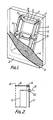
- FIG. 1 it represents a seven stroke character arranged to display a stylised numeral eight.
- Stylised characters of this kind are now very well known, and by selectively energising different combinations of strokes, any of the numerals nought to nine can be formed.
- the arrangement comprises a sealed envelope 1 in the form of a thin rectangular box having a front plate 2, which carries a fluorescent screen 3 upon its inner surface.
- a mesh electrode 4 is mounted immediately in front of the screen 3, but is spaced apart slightly from it and mounted so as to be electrically insulated from the screen.
- the envelope 1 is formed of glass which intrinsically is an excellent electrical insulator. This is an important consideration as, in operation, a potential difference of several thousand volts exists between the fluorescent screen 3 and the mesh electrode 4.
- a cathode structure is mounted closely behind the mesh electrode 4, and the cathode structure consists of several individual cathode filaments 5 mounted under tension between a pair of conductive pins 6, which project through respective field electrodes 7, which take the form of conductive back plates. Each cathode filament 5 is surrounded by conductive walls 8, which are attached to the back plates and which lie between the field electrode 7 and the mesh electrode 4. The mesh electrode is electrically insulated from the walls 8.
- the field electrode 7, the cathode filaments 5, and the mesh electrode 4 operate at different electrical potentials and it is therefore important that the walls 8 do not electrically connect them.
- the walls 8 can conveniently be physically attached to the field electrode 7, so that together they form an open box like container within which the cathode filaments 5 are situated.
- FIG. 2 An alternative construction, which is preferred, is illustrated in Figure 2.
- the walls 8 provide the support for the mesh electrode 4, which is attached to its outer edges.
- the field electrode 7 consists solely of the back plate through which the pins 6 pass. These pins 6 are electrically insulated from the back plate by means of insulating bushes 10 or the like.
- the walls 8 can be mounted upon the back plates, which constitute the field electrodes 7 by means of electrically insulating spacers 9.
- FIG. 1 Although, in Figure 1, seven individual cathode filaments are shown, an alternative construction can be used in which an arbitrary number of filaments can be stretched across the back surface of the display arrangement, so as to be mounted above localised back plates of the kind shown in Figure 1. Walls of the kind shown in Figure 1, but electrically insulated from the various electrodes, would also be provided in this case, as the walls serve to act as a stencil, and ensure that only predetermined areas of the screen 3 are reached by electrons originating at particular cathodes. This enables a very sharp pattern to be displayed which does not have blurred edges.
- the fluorescent screen 3 is held at a constant potential of about +7 kilovolts, and the mesh electrode 4 is held at a potential of about +10 volts, with respect to the nominal cathode potential. Whilst a display segment is in its "on" state, i.e. whilst light is emitted, the corresponding cathode filament 5 is held at nought volts, and the field electrode 7 is held at +5 volts. Under these considerations the electric field in which the cathode filament 5 is situated is positive with respect to the cathode potential itself, so that electrons are copiously emitted. These electrons are attached to the mesh electrode 4, since it is held at a positive potential which is greater than that of the field electrode 7.
- the mesh electrode 4 consists of an array, net or grid of very fine wires, which are spaced apart from each other, so as to be largely physically transparent to electrons.
- the cathode most of the electrons emitted by the cathode reach the screen 3, thereby causing it to fluoresce and emit intense light.
- the potential on the cathode filament 5 is raised to about +10 volts as compared to its previous value, and the potential on the field electrode 7 is altered to -5 volts.
- the cathode is now situated in a field, (as determined by the potentials on the field electrode 7 and the mesh electrode 4) which is more negative than the potential on the cathode itself. Electron emission is therefore inhibited and virtually no free electrons are available to be accelerated to the mesh electrode 4.
- the physical spacing and configuration of the field electrode 7 with respect to the mesh electrode is of great importance, and in practice it is arranged that the cathode is very much closer to the field electrode than to the mesh electrode, so that the effect of the field electrode predominates.
- the shape and position of the field electrode 7 with respect to the cathode filament 5 is carefully chosen so that whilst a display segment is in its "on" state, electrons are emitted from the cathode in the form of a divergent flood beam which falls or impinges upon a predetermined locality or area of the mesh electrode. Electrons are accelerated from this locality of the mesh electrode to strike the fluorescent screen 3, and thus to a large extent the area of illumination is determined by the width or solid angle of the divergent flood beam of electrons. This width is also very dependent on the value of the potential difference of the field electrode with respect to that of the cathode. The potential difference during the "off" state which suppresses electron emission is less critical since it is merely necessary to ensure that the field in which the cathode filament is situated has a sufficiently negative value.
- FIG. 3 An alternative display arrangement is partly shown in Figure 3. Only the cathode structure and the associated field electrodes are shown, and in practice, a continuous mesh electrode is positioned between the cathode structure and a large fluorescent screen.
- the arrangement is capable of being operated as a matrix type display; that is to say, a number of individual localised patches of light can be produced which together represent the required display pattern.
- the cathode structure consists of seven elongate cathode filaments 11 to 17. Each filament passes through the five field electrode structures 18 to 22, which take the form of open trough like structures with internal partitions. Each field electrode is similar to the others, and consists of two upright major conductive walls 23 and 24 and two upright end conductive walls 25 and 26. A conductive base 27 is connected to the bottom edges of the four walls, and each of the open trough like structures is divided into seven smaller enclosures by six individual partitions 28. Small cut outs are provided at the lower surface of the major walls 23 and 24 to allow the filaments 11 to 17 to pass through without making electrical contact therewith, so that in operation the filaments can be operated at different potentials from those on the field electrodes.
- a continuous large mesh electrode is positioned in front of the open trough like structures, but mounted so as to be electrically insulated therefrom, and in a manner which is analogous to Figure 1, a fluorescent screen is positioned in front of this mesh electrode.
- the five separate field electrodes 18 to 22 and the seven cathode filaments 11 to 17 are in a crossing relationship with each other, having a total of thirty five individual crossing points.
- the display arrangement can be operated so as to produce in selected combination of thirty five light patches on the fluorescent screen which correspond to the crossing points.
- a constant potential of +10 volts is applied to the mesh electrode.
- a voltage of +5 volts is applied to that field electrode and nought volts to that particular filament.
- a bright patch is then produced on the fluorescent screen above the point where the filament and field electrode cross.
- the remaining cathodes are held at +10 volts and the remaining field electrodes are held at -5 volts.
- the filaments are heated by passing an a.c. current through them from a 3 volt supply.
- the frequency of the alternating current is chosen so as to avoid flicker frequencies resulting from interference with frequencies used to address the cathode filaments and the field electrodes.
- the addressing frequencies are a few hundred hertz, and the frequency of the a.c. current could conveniently be a few kilohertz.
- FIG. 4 and 5 A further form of the display arrangement is shown in Figure 4 and 5, in which a part perspective view and section view of a column display are shown.
- a device consists of a single tubular glass envelope 30 carrying five or more curved field electrodes 31 to 35 upon an inner surface thereof, and a single elongate cathode filament 36 positioned along the length of the envelope.
- the envelope 30 is formed in two halves, and a single long strip of mesh electrode 38 is positioned between them.
- a region of the upper half of the envelope is provided with a fluorescent coating, upon its inner surface, which thereby acts as a fluorescent screen 39.
- Such a tube is capable of selectively energising any one or more of five discrete regions of the upper half of the glass envelope.
- the mesh electrode 38 is held at a constant potential of +10 volts and the field electrodes 31 to 35 are switched between -5 volts (to inhibit electron emission) to +5 volts (when illumination is required).
- This particular form of construction is very simple to implement as the field electrode may simply be formed as conductive depositions upon the inner surface of the glass envelope.
- a number of these column displays can be assembled to form a large two dimensional array of separately controllable light patches.
Landscapes
- Cathode-Ray Tubes And Fluorescent Screens For Display (AREA)
- Electric Clocks (AREA)
- Devices For Indicating Variable Information By Combining Individual Elements (AREA)
- Investigating Or Analysing Materials By The Use Of Chemical Reactions (AREA)
Abstract
Description
- This invention relates to a display arrangement which is capable of presenting bright, but readily alterable displays with modest power consumption and without being excessively bulky.
- According to the first aspect of this invention a method of operating a display arrangement which includes a sealed envelope containing a mesh electrode positioned between an electron emissive cathode which is arranged to emit a divergent flood beam of electrons and a fluorescent screen which forms part of the envelope so that the flood beam falls upon a predetermined area of said mesh electrode; and field electrode means which is positioned so that the cathode is between at least a part of said means and said mesh electrode, the field electrode means being positioned closely adjacent to the cathode such that the potential difference between the field electrode means and the cathode influences the strength and polarity of the electric field in which the cathode is situated; includes sequential steps of (a) applying a first predetermined potential difference between the field electrode means and the cathode so as to cause the divergent flood beam of electrons of predetermined size to be emitted from said cathode so as to cause fluorescence of said screen; and (b) applying a second selectable predetermined potential difference between the field electrode means and the cathode so as to prevent electrons reaching the mesh electrode.
- According to a second aspect of this invention, a display arrangement includes a sealed envelope containing a mesh electrode positioned between an electron emissive cathode arranged to emit a divergent flood beam of electrons and a fluorescent screen which forms part of the envelope so that the flood beam falls upon a predetermined area of said mesh electrode; and field electrode means positioned so that the cathode is between at least a part of said means and said mesh electrode, the field electrode means being positioned closely adjacent to the cathode such that the potential difference between the field electrode means and the cathode influences the strength of the electric field in which the cathode is situated, characterised in that means are provided to alter said potential difference between two predetermined values so as to switch the polarity of said electric field between two states, in one state of which the flood beams of electrons reaches said screen to cause it to fluoresce and in the other state of which electrons do not reach said screen.
- According to a third aspect of this invention a display arrangement includes a sealed envelope containing mesh electrode means positioned between electron emissive cathode means which is arranged to emit electrons and a fluorescent screen which forms part of the envelope so that the electrons fall upon said mesh electrode means; and field electrode means characterised in that the field electrode means is positioned so that the cathode means is between at least a part of said field electrode means and said mesh electrode, the field electrode means being positioned closely adjacent to the cathode means such that a potential difference between the field electrode means and the cathode means influences the strength and polarity of the electric field in which the cathode means is situated, and wherein a plurality of electron emissive cathodes or a plurality of field electrodes are provided for independently altering selected regions of said electric field between two values to respectively generate or suppress a plurality of divergent flood beams of electrons each beam of which is directed to a different region of said screen to cause it to fluoresce.
- The strength and polarity of the electric field in which the electron emissive cathode is situated is dependent on the potential of the cathode itself as well as the potentials on the mesh electrode and the field electrode. Since the potential on the mesh electrode is primarily dictated by other considerations, it is preferable to use the potential upon the field electrode to control the passage of electrons from the cathode to the fluorescent screen. By arranging that the electron emissive cathode is situated in an electric field which is more negative than the potential of the cathode, free electron emission is inhibited, and electrons are tightly confined to the vicinity of the cathode surface and thus are unable to reach the fluorescent screen. Conversely by altering the polarity of the electric field with respect to the cathode, electrons are freely emitted and accelerated towards the mesh electrode which is at a potential somewhat more positive than that of the cathode. Once they reach this mesh electrode the electrons are rapidly accelerated towards the fluorescent screen, which typically has a potential of several thousand volts upon it. Increasing the magnitude of the electric field provides a control over the quantity of electrons which reach the screen and hence the brightness of the display, although the brightness is primarily dependent on the magnitude of the accelerating potential on the screen. The presence of the mesh electrode effectively isolates the cathode and the field grid from the effects of the high potential on the screen, and thus the display can be switched on and off by means of very low voltages in a rapid and reliable fashion.
- UK Patent Application GB-A-2058444 discloses a display arrangement in which a fluorescent screen is mounted in front of a filamentary cathode, with a conductive coating being positioned partly behind the cathode. This cathode is not positioned such that it can be operative to turn on and off the display. A constant potential of 5 V (with respect to the cathode) is applied to this conductive coating to give a more uniform illumination of the screen.
- The invention avoids the need to position control electrodes between a cathode structure and the screen to achieve selective illumination thereof, and it permits the thickness of a display arrangement to be very small indeed, since the control electrode, which comprises, in effect, the field electrode, can be positioned on that side of the cathode which is remote from the screen. Advantageously, one or both of the cathode and the field electrode are of a segmented nature, so that the selection of particular segments constrains electrons to call upon selected locations of the screen to permit complex display patterns to be generated and rapidly altered. In principle, the mesh electrode can be of a segmented nature, so that it can also be used to selectively address locations of the fluorescent screen, but this is less preferred.
- The display arrangements can take a number of different physical forms. For example, it can be arranged to generate a stylised symbol or character, usually a seven stroke character based upon the numeral eight. Alternatively, it can be used to select from a matrix of possible points or small patches of light just those points which act together to represent the required display pattern. Other variations are described subsequently with reference to the drawings. The use of an appropriate fluorescent screen enables a colour display to be provided, if necessary.
- The invention is further described by way of example with reference to the accompanying drawings, in which:
- Figure 1 shows a display arrangement in accordance with the invention,
- Figure 2 shows part of it in greater detail,
- Figure 3 shows part of a matrix display in accordance with the invention, and
- Figures 4 and 5 show an elongate display having a number of contiguous sections which can be selectively energised.
- Referring to Figure 1, it represents a seven stroke character arranged to display a stylised numeral eight. Stylised characters of this kind are now very well known, and by selectively energising different combinations of strokes, any of the numerals nought to nine can be formed. The arrangement comprises a sealed envelope 1 in the form of a thin rectangular box having a front plate 2, which carries a
fluorescent screen 3 upon its inner surface. Amesh electrode 4 is mounted immediately in front of thescreen 3, but is spaced apart slightly from it and mounted so as to be electrically insulated from the screen. Typically, the envelope 1 is formed of glass which intrinsically is an excellent electrical insulator. This is an important consideration as, in operation, a potential difference of several thousand volts exists between thefluorescent screen 3 and themesh electrode 4. A cathode structure is mounted closely behind themesh electrode 4, and the cathode structure consists of severalindividual cathode filaments 5 mounted under tension between a pair of conductive pins 6, which project throughrespective field electrodes 7, which take the form of conductive back plates. Eachcathode filament 5 is surrounded byconductive walls 8, which are attached to the back plates and which lie between thefield electrode 7 and themesh electrode 4. The mesh electrode is electrically insulated from thewalls 8. - In operation, the
field electrode 7, thecathode filaments 5, and themesh electrode 4 operate at different electrical potentials and it is therefore important that thewalls 8 do not electrically connect them. Thewalls 8 can conveniently be physically attached to thefield electrode 7, so that together they form an open box like container within which thecathode filaments 5 are situated. - An alternative construction, which is preferred, is illustrated in Figure 2. In this arrangement, the
walls 8 provide the support for themesh electrode 4, which is attached to its outer edges. In this case thefield electrode 7 consists solely of the back plate through which the pins 6 pass. These pins 6 are electrically insulated from the back plate by means of insulatingbushes 10 or the like. In practice, thewalls 8 can be mounted upon the back plates, which constitute thefield electrodes 7 by means of electrically insulating spacers 9. - Although, in Figure 1, seven individual cathode filaments are shown, an alternative construction can be used in which an arbitrary number of filaments can be stretched across the back surface of the display arrangement, so as to be mounted above localised back plates of the kind shown in Figure 1. Walls of the kind shown in Figure 1, but electrically insulated from the various electrodes, would also be provided in this case, as the walls serve to act as a stencil, and ensure that only predetermined areas of the
screen 3 are reached by electrons originating at particular cathodes. This enables a very sharp pattern to be displayed which does not have blurred edges. - In operation, the
fluorescent screen 3 is held at a constant potential of about +7 kilovolts, and themesh electrode 4 is held at a potential of about +10 volts, with respect to the nominal cathode potential. Whilst a display segment is in its "on" state, i.e. whilst light is emitted, thecorresponding cathode filament 5 is held at nought volts, and thefield electrode 7 is held at +5 volts. Under these considerations the electric field in which thecathode filament 5 is situated is positive with respect to the cathode potential itself, so that electrons are copiously emitted. These electrons are attached to themesh electrode 4, since it is held at a positive potential which is greater than that of thefield electrode 7. As soon as the electrons pass through themesh electrode 4 they are very rapidly accelerated under the influence of the high voltage present on thescreen 3. In practice, themesh electrode 4 consists of an array, net or grid of very fine wires, which are spaced apart from each other, so as to be largely physically transparent to electrons. Thus, in practice, most of the electrons emitted by the cathode reach thescreen 3, thereby causing it to fluoresce and emit intense light. - Conversely, in order to turn the display "off", i.e. so that it is dark, the potential on the
cathode filament 5 is raised to about +10 volts as compared to its previous value, and the potential on thefield electrode 7 is altered to -5 volts. The cathode is now situated in a field, (as determined by the potentials on thefield electrode 7 and the mesh electrode 4) which is more negative than the potential on the cathode itself. Electron emission is therefore inhibited and virtually no free electrons are available to be accelerated to themesh electrode 4. In order to ensure that the electric field is sufficiently negative at the cathode, the physical spacing and configuration of thefield electrode 7 with respect to the mesh electrode is of great importance, and in practice it is arranged that the cathode is very much closer to the field electrode than to the mesh electrode, so that the effect of the field electrode predominates. - The shape and position of the
field electrode 7 with respect to thecathode filament 5 is carefully chosen so that whilst a display segment is in its "on" state, electrons are emitted from the cathode in the form of a divergent flood beam which falls or impinges upon a predetermined locality or area of the mesh electrode. Electrons are accelerated from this locality of the mesh electrode to strike thefluorescent screen 3, and thus to a large extent the area of illumination is determined by the width or solid angle of the divergent flood beam of electrons. This width is also very dependent on the value of the potential difference of the field electrode with respect to that of the cathode. The potential difference during the "off" state which suppresses electron emission is less critical since it is merely necessary to ensure that the field in which the cathode filament is situated has a sufficiently negative value. - An alternative display arrangement is partly shown in Figure 3. Only the cathode structure and the associated field electrodes are shown, and in practice, a continuous mesh electrode is positioned between the cathode structure and a large fluorescent screen. The arrangement is capable of being operated as a matrix type display; that is to say, a number of individual localised patches of light can be produced which together represent the required display pattern.
- The cathode structure consists of seven
elongate cathode filaments 11 to 17. Each filament passes through the fivefield electrode structures 18 to 22, which take the form of open trough like structures with internal partitions. Each field electrode is similar to the others, and consists of two upright majorconductive walls conductive walls individual partitions 28. Small cut outs are provided at the lower surface of themajor walls filaments 11 to 17 to pass through without making electrical contact therewith, so that in operation the filaments can be operated at different potentials from those on the field electrodes. - As previously mentioned, a continuous large mesh electrode is positioned in front of the open trough like structures, but mounted so as to be electrically insulated therefrom, and in a manner which is analogous to Figure 1, a fluorescent screen is positioned in front of this mesh electrode. The five
separate field electrodes 18 to 22 and the sevencathode filaments 11 to 17 are in a crossing relationship with each other, having a total of thirty five individual crossing points. - The display arrangement can be operated so as to produce in selected combination of thirty five light patches on the fluorescent screen which correspond to the crossing points. In operation, a constant potential of +10 volts is applied to the mesh electrode. To illuminate a single selected light patch corresponding to the crossing point of a cathode filament and a field electrode, a voltage of +5 volts is applied to that field electrode and nought volts to that particular filament. A bright patch is then produced on the fluorescent screen above the point where the filament and field electrode cross. The remaining cathodes are held at +10 volts and the remaining field electrodes are held at -5 volts. These potentials ensure that electron emission from the cathode filaments is inhibited at all of the other corresponding thirty four possible patches of illumination.
- In practice, these potentials are only approximate since optimum values will depend on the sizes and shapes of the various electrodes and cathode filaments which are used. Conveniently, the filaments are heated by passing an a.c. current through them from a 3 volt supply. The frequency of the alternating current is chosen so as to avoid flicker frequencies resulting from interference with frequencies used to address the cathode filaments and the field electrodes. Typically, the addressing frequencies are a few hundred hertz, and the frequency of the a.c. current could conveniently be a few kilohertz.
- It will be appreciated that altering the potential on the filaments between the two values of nought volts and +10 volts to produce selective illuminating of the screen does not affect the temperature of the filaments, since this is a constant value determined by the magnitude of the a.c. currents flowing through them.
- A further form of the display arrangement is shown in Figure 4 and 5, in which a part perspective view and section view of a column display are shown. Such a device consists of a single
tubular glass envelope 30 carrying five or morecurved field electrodes 31 to 35 upon an inner surface thereof, and a singleelongate cathode filament 36 positioned along the length of the envelope. Theenvelope 30 is formed in two halves, and a single long strip ofmesh electrode 38 is positioned between them. A region of the upper half of the envelope is provided with a fluorescent coating, upon its inner surface, which thereby acts as afluorescent screen 39. Such a tube is capable of selectively energising any one or more of five discrete regions of the upper half of the glass envelope. In operation, themesh electrode 38 is held at a constant potential of +10 volts and thefield electrodes 31 to 35 are switched between -5 volts (to inhibit electron emission) to +5 volts (when illumination is required). - This particular form of construction is very simple to implement as the field electrode may simply be formed as conductive depositions upon the inner surface of the glass envelope. A number of these column displays can be assembled to form a large two dimensional array of separately controllable light patches.
Claims (10)
Priority Applications (1)
| Application Number | Priority Date | Filing Date | Title |
|---|---|---|---|
| AT83304140T ATE27749T1 (en) | 1982-08-06 | 1983-07-15 | INDICATOR. |
Applications Claiming Priority (2)
| Application Number | Priority Date | Filing Date | Title |
|---|---|---|---|
| GB8222740 | 1982-08-06 | ||
| GB8222740 | 1982-08-06 |
Publications (3)
| Publication Number | Publication Date |
|---|---|
| EP0101195A2 EP0101195A2 (en) | 1984-02-22 |
| EP0101195A3 EP0101195A3 (en) | 1984-08-29 |
| EP0101195B1 true EP0101195B1 (en) | 1987-06-10 |
Family
ID=10532162
Family Applications (1)
| Application Number | Title | Priority Date | Filing Date |
|---|---|---|---|
| EP83304140A Expired EP0101195B1 (en) | 1982-08-06 | 1983-07-15 | Display arrangements |
Country Status (6)
| Country | Link |
|---|---|
| US (1) | US4623882A (en) |
| EP (1) | EP0101195B1 (en) |
| JP (1) | JPS5963645A (en) |
| AT (1) | ATE27749T1 (en) |
| DE (1) | DE3372042D1 (en) |
| GB (1) | GB2124825B (en) |
Families Citing this family (7)
| Publication number | Priority date | Publication date | Assignee | Title |
|---|---|---|---|---|
| JPH0640474B2 (en) * | 1985-07-08 | 1994-05-25 | 伊勢電子工業株式会社 | Display tube for light source |
| USD304349S (en) | 1987-02-27 | 1989-10-31 | Leger Jean P | Electronic display panel |
| JPH01100854A (en) * | 1987-10-12 | 1989-04-19 | Mitsubishi Electric Corp | Fluorescent character display |
| JPH0745218A (en) * | 1993-05-26 | 1995-02-14 | Matsushita Electric Ind Co Ltd | Flat image display device |
| GB2306039B (en) * | 1995-10-02 | 1999-09-29 | Dewhurst Plc | Light display and method of forming the same |
| JP3063637B2 (en) * | 1996-09-19 | 2000-07-12 | 双葉電子工業株式会社 | Color display |
| US5982550A (en) * | 1998-06-17 | 1999-11-09 | Chrylser Corporation | Viewing angle lens |
Family Cites Families (15)
| Publication number | Priority date | Publication date | Assignee | Title |
|---|---|---|---|---|
| NL264779A (en) * | 1960-05-16 | |||
| NL278584A (en) | 1961-05-19 | |||
| US3673448A (en) | 1968-10-12 | 1972-06-27 | Ise Electronics Corp | Cathode ray tubes having row and column electrodes attached to opposite sides of insulating substrate |
| US3622828A (en) * | 1969-12-01 | 1971-11-23 | Us Army | Flat display tube with addressable cathode |
| JPS5047564A (en) | 1973-07-31 | 1975-04-28 | ||
| US4029984A (en) * | 1975-11-28 | 1977-06-14 | Rca Corporation | Fluorescent discharge cold cathode for an image display device |
| US4004186A (en) | 1975-12-01 | 1977-01-18 | Texas Instruments Incorporated | Vacuum fluorescent display having a grid plate coplanar with the anode |
| JPS569230Y2 (en) | 1976-01-28 | 1981-02-28 | ||
| GB1536776A (en) * | 1976-07-10 | 1978-12-20 | English Electric Valve Co Ltd | Display arrangements |
| US4227117A (en) * | 1978-04-28 | 1980-10-07 | Matsuhita Electric Industrial Co., Ltd. | Picture display device |
| GB2031220B (en) * | 1978-10-04 | 1983-01-06 | English Electric Valve Co Ltd | Evacuated display tubes |
| GB2031219B (en) | 1978-10-04 | 1982-12-01 | English Electric Valve Co Ltd | Crt matrix display |
| US4280125A (en) | 1979-07-27 | 1981-07-21 | Xerox Corporation | Thin vacuum panel display device |
| GB2058444B (en) * | 1979-09-06 | 1983-06-08 | English Electric Valve Co Ltd | Display arramgements |
| US4263529A (en) | 1979-10-22 | 1981-04-21 | Rca Corp. | Modulator with variable launch conditions for multi-electron gun display devices |
-
1983
- 1983-07-13 GB GB08318922A patent/GB2124825B/en not_active Expired
- 1983-07-15 EP EP83304140A patent/EP0101195B1/en not_active Expired
- 1983-07-15 DE DE8383304140T patent/DE3372042D1/en not_active Expired
- 1983-07-15 AT AT83304140T patent/ATE27749T1/en not_active IP Right Cessation
- 1983-08-04 US US06/520,248 patent/US4623882A/en not_active Expired - Fee Related
- 1983-08-05 JP JP58143621A patent/JPS5963645A/en active Pending
Also Published As
| Publication number | Publication date |
|---|---|
| GB2124825A (en) | 1984-02-22 |
| EP0101195A2 (en) | 1984-02-22 |
| US4623882A (en) | 1986-11-18 |
| JPS5963645A (en) | 1984-04-11 |
| GB2124825B (en) | 1986-03-26 |
| EP0101195A3 (en) | 1984-08-29 |
| ATE27749T1 (en) | 1987-06-15 |
| GB8318922D0 (en) | 1983-08-17 |
| DE3372042D1 (en) | 1987-07-16 |
Similar Documents
| Publication | Publication Date | Title |
|---|---|---|
| US4243986A (en) | Display arrangements | |
| KR100238742B1 (en) | Image display device having a vacuum enclosure | |
| US4459514A (en) | Fluorescent display device | |
| GB2110466A (en) | Display device | |
| JP2001166725A (en) | Fluorescent display tube and its driving method | |
| US4623882A (en) | Fluorescent display arrangement having field electrode adjacent cathode | |
| US4387322A (en) | Display arrangements | |
| US4306178A (en) | Display arrangements | |
| US4368404A (en) | Matrix-type fluorescent display device | |
| US4733139A (en) | Fluorescent display device | |
| US5949395A (en) | Flat-panel matrix-type light emissive display | |
| US4893056A (en) | Fluorescent display apparatus | |
| US4695765A (en) | Display arrangements | |
| US4193014A (en) | Display arrangements | |
| US4617491A (en) | Fluorescent display device with interleaved anode and control electrode segments | |
| US4695764A (en) | Display arrangements | |
| US3249802A (en) | Electronic glow-discharge indicator | |
| US4232251A (en) | Multi-digit luminescent display tube | |
| KR890011000A (en) | Flat cathode ray tube display device | |
| JPS6124867B2 (en) | ||
| GB1569973A (en) | Display arrangements | |
| RU2272332C2 (en) | Cathodic-luminescent matrix screen | |
| RU2172998C1 (en) | Matrix-type luminescent cathodic screen | |
| DE2105496C3 (en) | Gas discharge indicator | |
| JPH0119802Y2 (en) |
Legal Events
| Date | Code | Title | Description |
|---|---|---|---|
| PUAI | Public reference made under article 153(3) epc to a published international application that has entered the european phase |
Free format text: ORIGINAL CODE: 0009012 |
|
| AK | Designated contracting states |
Designated state(s): AT BE CH DE FR IT LI LU NL SE |
|
| PUAL | Search report despatched |
Free format text: ORIGINAL CODE: 0009013 |
|
| AK | Designated contracting states |
Designated state(s): AT BE CH DE FR IT LI LU NL SE |
|
| 17P | Request for examination filed |
Effective date: 19840724 |
|
| GRAA | (expected) grant |
Free format text: ORIGINAL CODE: 0009210 |
|
| AK | Designated contracting states |
Kind code of ref document: B1 Designated state(s): AT BE CH DE FR IT LI LU NL SE |
|
| PG25 | Lapsed in a contracting state [announced via postgrant information from national office to epo] |
Ref country code: IT Free format text: LAPSE BECAUSE OF FAILURE TO SUBMIT A TRANSLATION OF THE DESCRIPTION OR TO PAY THE FEE WITHIN THE PRESCRIBED TIME-LIMIT;WARNING: LAPSES OF ITALIAN PATENTS WITH EFFECTIVE DATE BEFORE 2007 MAY HAVE OCCURRED AT ANY TIME BEFORE 2007. THE CORRECT EFFECTIVE DATE MAY BE DIFFERENT FROM THE ONE RECORDED. Effective date: 19870610 Ref country code: AT Effective date: 19870610 |
|
| REF | Corresponds to: |
Ref document number: 27749 Country of ref document: AT Date of ref document: 19870615 Kind code of ref document: T |
|
| PG25 | Lapsed in a contracting state [announced via postgrant information from national office to epo] |
Ref country code: SE Effective date: 19870630 |
|
| REF | Corresponds to: |
Ref document number: 3372042 Country of ref document: DE Date of ref document: 19870716 |
|
| ET | Fr: translation filed | ||
| PG25 | Lapsed in a contracting state [announced via postgrant information from national office to epo] |
Ref country code: LU Free format text: LAPSE BECAUSE OF NON-PAYMENT OF DUE FEES Effective date: 19870731 |
|
| PLBE | No opposition filed within time limit |
Free format text: ORIGINAL CODE: 0009261 |
|
| STAA | Information on the status of an ep patent application or granted ep patent |
Free format text: STATUS: NO OPPOSITION FILED WITHIN TIME LIMIT |
|
| 26N | No opposition filed | ||
| PGFP | Annual fee paid to national office [announced via postgrant information from national office to epo] |
Ref country code: BE Payment date: 19890612 Year of fee payment: 7 |
|
| PGFP | Annual fee paid to national office [announced via postgrant information from national office to epo] |
Ref country code: FR Payment date: 19900619 Year of fee payment: 8 Ref country code: CH Payment date: 19900619 Year of fee payment: 8 |
|
| PG25 | Lapsed in a contracting state [announced via postgrant information from national office to epo] |
Ref country code: BE Effective date: 19900731 |
|
| PGFP | Annual fee paid to national office [announced via postgrant information from national office to epo] |
Ref country code: NL Payment date: 19900731 Year of fee payment: 8 |
|
| PGFP | Annual fee paid to national office [announced via postgrant information from national office to epo] |
Ref country code: DE Payment date: 19900827 Year of fee payment: 8 |
|
| PGFP | Annual fee paid to national office [announced via postgrant information from national office to epo] |
Ref country code: LU Payment date: 19900829 Year of fee payment: 8 |
|
| BERE | Be: lapsed |
Owner name: ENGLISH ELCTRIC VALVE CY LTD Effective date: 19900731 |
|
| PG25 | Lapsed in a contracting state [announced via postgrant information from national office to epo] |
Ref country code: LI Effective date: 19910731 Ref country code: CH Effective date: 19910731 |
|
| PG25 | Lapsed in a contracting state [announced via postgrant information from national office to epo] |
Ref country code: NL Effective date: 19920201 |
|
| NLV4 | Nl: lapsed or anulled due to non-payment of the annual fee | ||
| PG25 | Lapsed in a contracting state [announced via postgrant information from national office to epo] |
Ref country code: FR Effective date: 19920331 |
|
| REG | Reference to a national code |
Ref country code: CH Ref legal event code: PL |
|
| PG25 | Lapsed in a contracting state [announced via postgrant information from national office to epo] |
Ref country code: DE Effective date: 19920401 |
|
| REG | Reference to a national code |
Ref country code: FR Ref legal event code: ST |