EP0096857B1 - Transmission filter with biquadratic filter stages - Google Patents
Transmission filter with biquadratic filter stages Download PDFInfo
- Publication number
- EP0096857B1 EP0096857B1 EP19830105677 EP83105677A EP0096857B1 EP 0096857 B1 EP0096857 B1 EP 0096857B1 EP 19830105677 EP19830105677 EP 19830105677 EP 83105677 A EP83105677 A EP 83105677A EP 0096857 B1 EP0096857 B1 EP 0096857B1
- Authority
- EP
- European Patent Office
- Prior art keywords
- input
- filter
- amplifier
- output
- transfer function
- Prior art date
- Legal status (The legal status is an assumption and is not a legal conclusion. Google has not performed a legal analysis and makes no representation as to the accuracy of the status listed.)
- Expired
Links
- 230000005540 biological transmission Effects 0.000 title claims description 26
- 239000003990 capacitor Substances 0.000 claims description 64
- 238000013016 damping Methods 0.000 claims description 5
- 238000005070 sampling Methods 0.000 claims description 5
- 230000035945 sensitivity Effects 0.000 description 6
- 230000003071 parasitic effect Effects 0.000 description 4
- 230000001419 dependent effect Effects 0.000 description 2
- 238000009499 grossing Methods 0.000 description 2
- 230000015572 biosynthetic process Effects 0.000 description 1
- 238000010586 diagram Methods 0.000 description 1
- 239000006185 dispersion Substances 0.000 description 1
- 239000011159 matrix material Substances 0.000 description 1
- 238000000034 method Methods 0.000 description 1
- 238000003786 synthesis reaction Methods 0.000 description 1
Images





Classifications
-
- H—ELECTRICITY
- H03—ELECTRONIC CIRCUITRY
- H03H—IMPEDANCE NETWORKS, e.g. RESONANT CIRCUITS; RESONATORS
- H03H19/00—Networks using time-varying elements, e.g. N-path filters
- H03H19/004—Switched capacitor networks
Definitions
- the present invention relates to a leapfrog filter including a plurality of biquadratic filter stages coupled in a leapfrog configuration.
- Such a filter is generally known in the art e.g. from the article "Synthesis of a leapfrog configuration equivalent to an LC-ladder filter between generalized terminations" by D. Dubois and J. Neirynck, published in the IEEE Transactions on Circuits and Systems, Vol. CAS-24, No. 11, November 1977, pp. 590-597.
- the scattering matrix S of such a 2-port defined with respect to real termination impedances W 1 and W 2 has the form where:
- the voltage transfer function f/2g is substantially equal to unity and ff-/gg- is substantially a constant.
- the function N/D should be as constant (or flat) as possible.
- this choice of N/D has merely permitted to place one pair of complex conjugate zeros of h onto the imaginary axis in the s-plane.
- a further object of the present invention is to provide a leapfrog filter of the above type, but which does not require N/D to be substantially constant (or flat) in the passband so as to reach therein a minimum sensitivity to filter component variations.
- the invention is based on the insight that when one puts an additional stage with transfer function in cascade with the input of the above mentioned lossless 2-port and thus multiplies the overall transfer function by this factor, it is necessary if the overall (unity) transfer function in the passband should remain unchanged to multiply ff-/gg- in the passband by about
- each termination stage and the adjacent stage of the two-part are combined to constitute a new biquadratic filter stage.
- Yet another characteristic feature of the present leapfrog filter is that it includes a biquadratic filter input stage with a first input constituting the input of the leapfrog filter, a second input and an output and includes a forward circuit between said first input and said output which realizes the transfer function of said first filter part and a feedback circuit between said second input and said output which realizes the transfer function of said first stage of said second filter part.
- the present invention also relates to a switched capacitor biquadratic filter circuit with an input and an output and including a non-overlapping two-phase clock source and first and second operational amplifiers each having an inverting input, a grounded non-inverting input, an output and a feedback capacitance, the output of said first amplifier being coupled to the input of said second amplifier via first capacitance means including a first capacitance the plates of which are connected to first and second change-over switches able, under the control of said clock source, to connect them between a ground and said output of said first amplifier and between said ground and the input of said second amplifier, the output of said second amplifier being coupled to the input of said first amplifier via second capacitance means including a second capacitance the plates of which are connected to third and fourth changeover switches able under the control of said clock source, to connect them between said ground and the output of said second amplifier and between said ground and said input of said first amplifier, and said filter input being coupled to an input of one of said amplifiers via third capacitance means including at least a third capacit
- Another object of the present invention is to provide switched capacitor biquadratic filter stages which are insensitive to parasitic capacitances and particularly adapted for use in leapfrog filters previously defined.
- such an object is achieved by a switched capacitor biquadratic filter wherein said clock source controls said switches in such a way that said second capacitor is connected to the input of said first amplifier and said first capacitor is connected to said input of said second amplifier for respective different phases of said clock source.
- the present invention also relates to a switched capacitor biquadratic filter circuit, characterized in that it simultaneously realizes a transfer function proportional to z z- 1 between a first input and an output and a second transfer function proportional to (z ⁇ 1) 2 between a second input and said output the transfer functions being considered in the z-plane.
- Such a filter circuit can thus be directly used to realize the above mentioned input stage of a leapfrog filter defined above.
- the subscriber line circuit SLC for a PCM telephone switching system shown in Fig. 1 includes a subscriber line interface circuit SLIC which is connected to a coder/decoder circuit or codec COD, operating at 8 kHz, via the cascade connection of an anti-aliasing transmit filter TIF, a transmit bandpass filter TBPF . and a smoothing transmit filter TOF, whilst the codec COD, is connected to the SLIC via the cascade connection of a receive lowpass filter RLPF and a smoothing receive filter ROF.
- a subscriber line interface circuit SLIC which is connected to a coder/decoder circuit or codec COD, operating at 8 kHz, via the cascade connection of an anti-aliasing transmit filter TIF, a transmit bandpass filter TBPF . and a smoothing transmit filter TOF, whilst the codec COD, is connected to the SLIC via the cascade connection of a receive lowpass filter RLPF and a smoothing receive filter ROF.
- the filters TIF, TOF, ROF all are of the second order Sallen-Key type.
- the bandpass filter TBPF is an eighth-order switched capacitor leapfrog filter operating as an anti-alias filter and rejecting 50 Hz and 60 Hz power supply frequencies.
- the lowpass filter RLPF is a fourth-order switched capacitor leapfrog filter having substantially the same lowpass characteristic as the TBPF and realizing a correction for the sampling operation in the codec. In both filters the capacitors ratio has a minimum dispersion and the filters have a small sensitivity to component variations and use a single clock frequency of 256 kHz.
- Switched capacitor filters for use in a subscriber line circuit for a PCM telephone switching system are already known from the following articles, both published in the IEEE Journal of Solid-State Circuits, Vol. SC-15, No. 6, December 1980, and entitled "A precision low-power PCM channel filter with on-chip power supply regulation" by H. Ohara et al, pp. 1005-1013, and "A low-power NMOS transmit-receive IC filter for PCM telephony" by I. A. Young, pp. 997-1005. None of these circuits however includes an eighth order leapfrog bandpass filter and a fourth order leapfrog lowpass filter.
- a structure comprising a 2-port which is lossless for reactive power and connected to terminations W 1 and W 2 which are dissipative for reactive power will now be considered.
- the power is pseudo power because it cannot be measured.
- This 2-port is constituted by a plurality of biquadratic filter stages T 1 to T m which are arranged in a leapfrog configuration. These stages have an infinite quality factor and transfer functions which are even functions because they are lossless for reactive power. On the contrary, the transfer functions of the termination stages W 1 and W 2 are odd functions because they are dissipative for reactive power.
- the circuit comprising ⁇ W 1 and the stage T 1 , on the one hand, and the circuit comprising ⁇ W 2 -1 and the stage Tm on the other hand can be realized by the biquadratic stages T' 1 and T' m respectively, the transfer functions of which are related to those of W 1 , T 1 and W 2 -1 , Tm by and
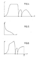
- the transfer function T shown in Fig. 4 is a combination of the transfer function e.g. of the additional stage AS (Fig. 3) and shown in Fig. 5 and of the transfer function represented in Fig. 6 of the filter part T' i , T 2 , T 3 , T' m (Fig. 3).
- the slope of Fig. 5 compensates that of Fig. 6 to provide the flat passband of Fig. 4.
- This inclined passband permits to place a maximum of attenuation zeros of the polynome h in this passband.
- T" 1 has a forward path with transfer function and a feedback path with transfer function p 1 being the denominator of T' 1 in the relation 13 given above.
- the transfer function of the forward path from IN to the output OUT of T' 1 is equal to when taking relation (13) into account, and the transfer function of the feedback path from point A to output OUT, is equal to
- Fig. 8 The structure of Fig. 8 will now be used to realize an 8th order bandpass leapfrog filter having a transfer function with an odd numerator and making use of switched capacitor biquadratic filter stages which are insensitive to parasitic capacitances.
- the internal biquadratic filter stages such as T 2 and T 3 of the above considered leapfrog filter have an infinite quality factor and a small sensitivity to component variations
- the biquadratic end stages T", and T' 4 are damped stages and should have a sensitivity which is as small as possible (for the quality factor).
- Such non-damped and damped stages are shown in Figs. 9 to 16 representing more particularly switched capacitor biquadratic stages which are each insensitive to parasitic capacitances.
- the biquadratic filter stage of Fig. 9 can be characterized as follows:
- biquadratic filter stages of Figures 10 to 16 can be characterized as follows:
- Biquadratic filter stage T is a combination, as explained above, or a forward circuit between IN and OUT, with transfer function and of a backward circuit between A and OUT 1 with transfer function
- Biquadratic stages T 2 and T 3 are of the type shown in Fig. 9 without damping capacitor k s C 2 . They have the respective transfer functions (see relation 15) with h 2 >0 with h 3 >0
- Figs. 15 and Fig. 9 only differ in the connection of their entries and therefore it was possible to use in Fig. 17 for T" 1 a same circuit with an input IN, constituting the input of the filter and connected as in Fig. 15, and with another input A connected as in Fig. 9. However, because the signal at the input A should be positive (see Fig. 8) but is negative at the output OUT 2 (see the transfer function of T 2 ) to which A is coupled a negative capacitor -Ca corresponding to k 4 C 2 in Fig. 9 has to be used.
- OUT 1 of T" 1 and the output OUT3 of T 3 are both connected to the input of T 2 via a summing circuit S 2 .
- the output OUT 1 is coupled to the inputs IN 21 and IN 22 of T 2 via capacitors C 8 and C 9 corresponding to k 3 C 1 and k 4 C 2 in Fig. 9 and the output OUT3 is coupled to the same inputs IN 21 and IN 22 via capacitors C 10 and C 11 respectively also corresponding to k 3 C, and k 4 C 2 in Fig. 9.
- the interconnections between the capacitors C 8 and C 10 as well as between the capacitors C 2 and -Ca constitute summing point S 1 in Fig. 8.
- output OUT 2 is coupled to the inputs IN 31 and IN 32 of T 3 via respective capacitors C 14 and C 15 corresponding to k 3 C, at k 4 C 2 in Fig. 9 and the output OUT is coupled to the same inputs IN 2 , and IN 22 via capacitors C 16 and C 17 corresponding to k 3 C 1 and k 4 C 2 in Fig. 9.
- the interconnections between the capacitors C 14 and C 16 as well as between the capacitors C 15 and C 17 constitute summing point S 3 in Fig. 8.
- the output OUT3 of T 3 is also connected to the input IN 42 via negative capacitor -Cb.
- a negative capacitor -Cb is required because the signal at the output OUT3 of T 3 is negative, as follows from the above given transfer function, whereas according to Fig. 8 the signal at the input of T' 4 should be positive.
- This filter has a transfer function versus frequency characteristic such as shown in Fig. 4. Part of the corresponding attenuation versus frequency characteristic is also represented in Fig. 18. The group delay versus frequency characteristic of the filter is shown in Fig. 19 and fully satisfies the CCITT recommendations as indicated by the gauge.
- the receive lowpass filter RLPF of Fig. 1 is represented in detail in Fig. 20 and includes biquadratic stages T' 1 and T' 2 of the type shown in Fig. 9 (damped version) and Fig. 10 (damped version) respectively.
- capacitors C 1 and C 2 correspond to capacitors k 3 C 1 and k 4 C 2 in Fig. 9 and capacitors C 8 and C 9 correspond to capacitors k 3 C 1 and k 4 C 2 in Fig.10.
- the output OUT of T' 2 is fed back to IN 12 and IN 22 of T' 1 via connections including capacitors C 3 and C 4 respectively.
- Part of the attenuation versus frequency characteristic of the filter of Fig. 20 is shown in Fig. 21. In the lower passband the above mentioned correction is visible.
Landscapes
- Engineering & Computer Science (AREA)
- Power Engineering (AREA)
- Networks Using Active Elements (AREA)
Description
- The present invention relates to a leapfrog filter including a plurality of biquadratic filter stages coupled in a leapfrog configuration.
- Such a filter is generally known in the art e.g. from the article "Synthesis of a leapfrog configuration equivalent to an LC-ladder filter between generalized terminations" by D. Dubois and J. Neirynck, published in the IEEE Transactions on Circuits and Systems, Vol. CAS-24, No. 11, November 1977, pp. 590-597. The numerator of the transfer function of such a filter is even and can only have pairs of real transmission zeros at z=1 and z=-1 in the z-plane. However, it may be necessary in some circumstances to have single real transmission zeros at z=+1 and/or at z=-1, e.g. for the realization of a bandpass filter.
- A first object of the present invention is to provide a leapfrog filter of the above type but having a transfer function with an odd numerator and more particularly with at least three real transmission zeros at z=±1 and at least one real transmission zero at z=+1 in the z-plane.
- Reference is now made to the above article and to that by M. Hasler published in the IEEE Transactions on Circuits and Systems, Vol. CAS-27, No. 7, July 1980,pp. 636-641, and entitled "A new class of RC-active filters using FDNR elements and generalized terminations". From these it follows that a leapfrog filter comprising a real reciprocal non-dissipative 2-port connected between real non-dissipative terminations has a minimum sensitivity to component variations at the frequencies where the frequency dependent filter polynomial h defined below is equal to zero, i.e. at the frequencies (attenuation zeros) where the maximum power transfer occurs (Orchard-Fettweis theorem).
- The scattering matrix S of such a 2-port defined with respect to real termination impedances W1 and W2 has the form

- N, D are coprime polynomials such that

- f, g and h are frequency dependent polynomials subject to the following conditions:
- f is even or odd and divisible by D and the upper sign of f corresponds to the upper sign of h_
- g is a strictly Hurwitz polynomial, i.e. its zeros are in the open left half of the s-plane;

- f_=f_(s)=f(―s)
- g-=g-(s)=g(-s)
- h-=h-(s)=h(-s)
a function with a - as subscript being the so-called Hurwitz conjugate of the function, i.e. a function of s wherein -s has been substituted for the complex frequency s. - In the filter passband and when it is substantially flat, the voltage transfer function f/2g is substantially equal to unity and ff-/gg- is substantially a constant. From the above relation (1) which is a related form of the Feldtkeller relation, it follows that in order to have a maximum number of zeros of h in the passband, the function N/D should be as constant (or flat) as possible. However, according to the article by M. Hasler, this choice of N/D has merely permitted to place one pair of complex conjugate zeros of h onto the imaginary axis in the s-plane.
- A further object of the present invention is to provide a leapfrog filter of the above type, but which does not require N/D to be substantially constant (or flat) in the passband so as to reach therein a minimum sensitivity to filter component variations.
- According to the invention the above objects are achieved due to the fact that the present leapfrog filter is a sampled filter with characteristics equivalent to those of a filter comprising the cascade connection of a first filter part having a transfer function proportional to

- Because the total transfer function of the filter is hence proportional


- The invention is based on the insight that when one puts an additional stage with transfer function


- From the above relation (1) it then follows that for sensitivity reasons, i.e. to have h equal to zero, one should take


- Due to N/D being no longer flat it has been possible to place a maximum number of zeros of h in the passband.
- Another characteristic feature of the present leapfrog filter is that the factor (z∓1)2 to which the transfer function of said first stage is proportional is the numerator of a function


- Still another characteristic feature of the present leapfrog filter is that the factor to which the transfer function of said last stage is proportional, is the numerator of a function


- Thus each termination stage and the adjacent stage of the two-part are combined to constitute a new biquadratic filter stage.
- Yet another characteristic feature of the present leapfrog filter is that it includes a biquadratic filter input stage with a first input constituting the input of the leapfrog filter, a second input and an output and includes a forward circuit between said first input and said output which realizes the transfer function of said first filter part and a feedback circuit between said second input and said output which realizes the transfer function of said first stage of said second filter part.
- . Thus a same biquadratic filter stage is used for realizing, on the one hand, the transfer function partly resulting from the additional stage with transfer function

- The present invention also relates to a switched capacitor biquadratic filter circuit with an input and an output and including a non-overlapping two-phase clock source and first and second operational amplifiers each having an inverting input, a grounded non-inverting input, an output and a feedback capacitance, the output of said first amplifier being coupled to the input of said second amplifier via first capacitance means including a first capacitance the plates of which are connected to first and second change-over switches able, under the control of said clock source, to connect them between a ground and said output of said first amplifier and between said ground and the input of said second amplifier, the output of said second amplifier being coupled to the input of said first amplifier via second capacitance means including a second capacitance the plates of which are connected to third and fourth changeover switches able under the control of said clock source, to connect them between said ground and the output of said second amplifier and between said ground and said input of said first amplifier, and said filter input being coupled to an input of one of said amplifiers via third capacitance means including at least a third capacitance.
- Such biquadratic filter stages realized in switched capacitor technique have already been designed and are for instance disclosed in the article "An NMOS analog building block for telecommunication applications" by P. E. Fleischer et al, published in IEEE Transaction on Circuits and Systems, Vol. CAS-27, No. 6, June 1980, pp. 552-559 and more particularly in Fig. 5 thereof.
- Another object of the present invention is to provide switched capacitor biquadratic filter stages which are insensitive to parasitic capacitances and particularly adapted for use in leapfrog filters previously defined.
- According to the invention such an object is achieved by a switched capacitor biquadratic filter wherein said clock source controls said switches in such a way that said second capacitor is connected to the input of said first amplifier and said first capacitor is connected to said input of said second amplifier for respective different phases of said clock source.
- The present invention also relates to a switched capacitor biquadratic filter circuit, characterized in that it simultaneously realizes a transfer function proportional to
z z-1 between a first input and an output and a second transfer function proportional to (z∓1)2 between a second input and said output the transfer functions being considered in the z-plane. - Such a filter circuit can thus be directly used to realize the above mentioned input stage of a leapfrog filter defined above.
- The above mentioned and other objects and features of the invention will become more apparent and the invention itself will be best understood by referring to the following description of embodiments taken in conjunction with the accompanying drawings wherein:
- Fig. 1 is a block diagram of a subscriber line circuit SLC for use in a PCM telephone system and incorporating leapfrog filters TBPF and RLPF according to the invention;
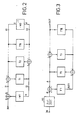
- Fig. 2 is a flowgraph of a classical leapfrog filter;
- Fig. 3 is a flowgraph of a leapfrog filter according to the invention;
- Figs. 4, 5 and 6 show transfer function versus frequency characteristics used to explain the invention;
- Fig. 7 is a flowgraph of a leapfrog filter according to the invention;
- Fig. 8 is a modified version of the flowgraph of Fig. 7;
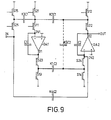
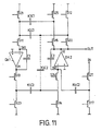
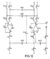
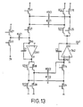
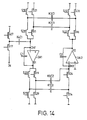
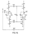
- Figs. 9 to 16 represent various switched capacitor biquadratic filter stages according to the invention;
- Fig. 17 shows the transmit bandpass filter TBPF of Fig. 1 in detail;
- Fig. 18 represents the attenuation versus frequency characteristic of the filter of Fig. 17;
- Fig. 19 shows the group delay versus frequency characteristic of the filter of Fig. 17;
- Fig. 20 represents the lowpass filter RLPF of Fig. 1 in detail;
- Fig. 21 shows the attenuation versus frequency characteristic of the filter of Fig. 20.
- The subscriber line circuit SLC for a PCM telephone switching system shown in Fig. 1 includes a subscriber line interface circuit SLIC which is connected to a coder/decoder circuit or codec COD, operating at 8 kHz, via the cascade connection of an anti-aliasing transmit filter TIF, a transmit bandpass filter TBPF . and a smoothing transmit filter TOF, whilst the codec COD, is connected to the SLIC via the cascade connection of a receive lowpass filter RLPF and a smoothing receive filter ROF.
- The filters TIF, TOF, ROF all are of the second order Sallen-Key type. The bandpass filter TBPF is an eighth-order switched capacitor leapfrog filter operating as an anti-alias filter and rejecting 50 Hz and 60 Hz power supply frequencies. The lowpass filter RLPF is a fourth-order switched capacitor leapfrog filter having substantially the same lowpass characteristic as the TBPF and realizing a

- Switched capacitor filters for use in a subscriber line circuit for a PCM telephone switching system are already known from the following articles, both published in the IEEE Journal of Solid-State Circuits, Vol. SC-15, No. 6, December 1980, and entitled "A precision low-power PCM channel filter with on-chip power supply regulation" by H. Ohara et al, pp. 1005-1013, and "A low-power NMOS transmit-receive IC filter for PCM telephony" by I. A. Young, pp. 997-1005. None of these circuits however includes an eighth order leapfrog bandpass filter and a fourth order leapfrog lowpass filter.
- A structure comprising a 2-port which is lossless for reactive power and connected to terminations W1 and W2 which are dissipative for reactive power will now be considered. In fact the power is pseudo power because it cannot be measured. This 2-port is constituted by a plurality of biquadratic filter stages T1 to Tm which are arranged in a leapfrog configuration. These stages have an infinite quality factor and transfer functions which are even functions because they are lossless for reactive power. On the contrary, the transfer functions of the termination stages W1 and W2 are odd functions because they are dissipative for reactive power. The termination stage W1 is connected in series with a generator e (having zero impedance) across the
input 11, I2 of the 2-port and thus provides a voltage e-W1I'1 (I'1 being the input current) across the input. In the flowgraph this is represented by the connection a=e-Wib. The termination stage W2 is connected across the output 01, O2 of the 2-port and thus provides a voltage v=W2I'2 (1'2 being the output current) across the output. Because
- As the stages T1 to Tm have an infinite quality factor,

- The circuit comprising ―W1 and the stage T1, on the one hand, and the circuit comprising ―W2 -1 and the stage Tm on the other hand can be realized by the biquadratic stages T'1 and T'm respectively, the transfer functions of which are related to those of W1, T1 and W2 -1, Tm by


- These end stages T'1 and T'm are shown in Fig. 3 (to be considered without the additional stage AS).
- In order that T'1 and T'm should be biquadratic functions the transmission poles of W1 should be the transmission zeros of T1 and the transmission poles of W2 -1 should be the transmission zeros of Tm. Moreover because W1 and W2 are dissipative for reactive power their transfer functions have to be odd. For this reason, W1 and W2 have been chosen as follows:


- By combining the relations (2) to (6) one obtains:


- From the relations (5) and (6) it follows that:

- From the above it also follows that the transfer function of the leapfrog filter shown in Fig. 3 (and considered without the stage AS) is of even order and has an even numerator.
- Reference is now made to the latter figure, but now with the additional stage AS having a transfer function equal to

- As already explained in the introduction, this additional stage leads to the following choice of the function N/D, i.e.

- To satisfy this relation, W1 and W2 (see previous relations 5 and 6) have now been chosen as follows:


- In this case T'1 and T'm (see previous relations (7) and (8) become:


- The numerator of the transfer function of the filter can therefore be written


- The structure of Fig. 3 permits, for instance, to realize a PCM bandpass filter operating at a sampling frequency fs and having a transfer function T/frequency characteristic such as shown in Fig. 4 i.e. with a flat passband and with three real zeros at frequency zero (DC) and one real zero at half the sampling frequency fs, i.e. in the z-plane at z=1 and at z=-1 respectively. The transfer function T shown in Fig. 4 is a combination of the transfer function e.g.


- The overall filter has three real transmission zeros at frequency zero and one real transmission zero at fs/2 because the transmission pole at z=+1 of Fig. 5 compensating a transmission zero at z=+1 of Fig. 4. On the other hand from Figs. 4 to 6 it also follows that in the passband the slope of Fig. 5 compensates that of Fig. 6 to provide the flat passband of Fig. 4. This inclined passband permits to place a maximum of attenuation zeros of the polynome h in this passband.
- The stages T'1 and AS in Fig. 3 can be realized by a single equivalent biquadratic filter stage T" shown in the flowgraph of Fig. 7 (where m=4). T"1 has a forward path with transfer function


relation 13 given above. Indeed, in the structure of Fig. 3 the transfer function of the forward path from IN to the output OUT of T'1 is equal to

- In the structure of Fig. 7 the signals at the summing points S2 and S3 have a different sign because the forward signals are plus signals, whereas the feedback signals are minus signals. For this reason the structure cannot be realized directly. On the other hand it is desirable to have as much negative signals as possible because biquadratic filter stages with a negative output signal (a negative h,) have been designed and are thus available, as will be explained later. Therefore the signals in the flowgraph of Fig. 7 have been manipulated to remove a maximum number of positive signals. The result is shown in Fig. 8 but is still not satisfactory because still two positive signals remain which will give rise to some difficulty because they require the use of non-existent negative capacitances.
- The structure of Fig. 8 will now be used to realize an 8th order bandpass leapfrog filter having a transfer function with an odd numerator and making use of switched capacitor biquadratic filter stages which are insensitive to parasitic capacitances.
- As mentioned above, the internal biquadratic filter stages such as T2 and T3 of the above considered leapfrog filter have an infinite quality factor and a small sensitivity to component variations, whereas the biquadratic end stages T", and T'4 are damped stages and should have a sensitivity which is as small as possible (for the quality factor). Such non-damped and damped stages are shown in Figs. 9 to 16 representing more particularly switched capacitor biquadratic stages which are each insensitive to parasitic capacitances. Some of these stages are known from the above mentioned article of P. E. Fleischer et al. Each of these stages makes use of:
- -two operational amplifiers OA1 and OA2;
- - two-phase clock (not shown) with non-overlapping phases;
- - MOS switches such as S11, S12,... and S21, S22,... the first indicia indicating the phase of the clock which has to be applied to close the switch;
- ―four capacitor connecting circuits which are insensitive to parasitic capacitors, i.e.
- = a first or non-inverting type, hereinafter called TP1, such as shown in the upper left part of Fig. 9 and able to connect a capacitor (k3C1) between an input (IN) and ground via switches (S25, S15) during one clock phase (here
clock phase 2 or CP2) and able to connect this capacitor between ground and an input (IN1) of an operational amplifier (OA1) via switches (S15, S11) during another clock phase (hereclock phase 1 or CP1); - = a second or inverting type, hereinafter called TP2, such as shown in the lower part of Fig. 9 and able to connect a capacitor (k1C2) between two grounds via switches (S13, S14) and during one clock phase (CP1) and able to connect this capacitor between an output (of OA1) and an input (IN2) of an operational amplifier (OA2) via switches (S23, S24) during another clock phase (CP2);
- = a third type, hereinafter called TP3, such as shown in Fig. 9 and connecting a capacitor (k4C2) directly to an input (IN2) of an operational amplifier (OA2);
- = a fourth type, hereinafter called TP4, such as shown in Fig. 11 and which includes a capacitor (k4C2) one plate of which is permanently connected to an input (IN2) of an operational amplifier (OA2) and the other plate of which can be connected to ground via a switch and during one clock phase (CP1). During the other clock phase the circuit is able to connect capacitor k4C2 between a circuit input (IN) and an input (IN2) of an operational amplifier (OA2).
- The biquadratic filter stage of Fig. 9 can be characterized as follows:
- - output O2 of OA2 is coupled to input IN1 of OA1 via a capacitor connecting circuit (S11, S21, S12, S22, k2C1) of type TP1 which connects capacitor k2C1 to IN1 on clock phase CP1;
- -input IN is coupled to IN1 via a capacitor connecting circuit (S11, S21, S15, S25) of type TP1 which connects capacitor k3C1 to IN, on clock phase CP1;
- - output O1 of OA1 is coupled to input IN2 of OA2 via a capacitor connecting circuit S13, S23, S14, S24, k1C2) of type TP2 which connects capacitor k1C2 to IN2 on clock phase CP2;
- - input IN is coupled to IN2 via a capacitor connecting circuit k4C2 of type TP3.
- Likewise, and in brief, the biquadratic filter stages of Figures 10 to 16 can be characterized as follows:
- Fig. 10: .
- O2 to IN1: TP2, CP1
- IN to IN1: TP2, CP1
- O1 to IN2: TP1, CP2
- IN to IN2: TP3
- Fig. 11:
- O2 to IN1: TP1 (k2C1), CP1
- O2 to IN1: TP2 (k3C1), CP1
- 01 to IN2: TP1, CP2
- IN to IN2: TP4, CP2
- Fig. 12:
- O2 to IN1: TP1 (k2C1), CP2
- O2 to IN1: TP1 (k3C1), CP1
- 01 to IN2: TP2, CP2
- IN1 to IN2: TP4, CP2
- Fig. 13:
- O2 to IN1: TP2 (k2C1), CP2
- O2 to IN1: TP1 (k3C1), CP2
- IN to IN1: TP4, CP2
- 01 to IN2: TP1 (k1C2), CP1
- O1 to IN2: TP4 (ksC2), CP2
- Fig. 14:
- O2 to IN1: TP1 (k2C1), CP1
- O2 to IN1: TP1 (k3C1), CP2
- IN to IN1: TP4, CP2
- O2 to IN2: TP2 (k1C2), CP2
- O2 to IN2: TP4 (k5C2), CP1
- Fig. 15:
- O2 to IN1: TP1, CP1
- IN to IN1: TP3
- O1 to IN2: TP2, CP2
- IN to IN1: TP3
- Fig. 16:
- O2 to IN1: TP2, CP1
- IN to IN1: TP3
- 01 to IN2: TP1, CP2
- IN to IN2: TP3
- All these biquadratic filter stages, except the one of Fig. 12 are characterized by the fact that the capacitors k1C2 and k2C1 are connected to IN2 and IN1 on different phases of the clock respectively. Afurther difference with the prior art is that different combinations of circuits TP1 to TP4 are used.
- The above biquadratic filter stages of Figs. 9 to 12 (to be considered without damping capacitor k3C2) have an infinite quality factor and a transfer function of the form

- and their components satisfy the following relations:
- ― Figs. 9 to 10 (without k5C2)
- k1k2=2 (1-cos tp)


- k1k2=2 (1-cos tp)
- - Fig. 11 (without k5C2)
- k1k2=2 (1-cos to)
- k1k3=2 (cos tP-cos to)
- k1k3=2 (cos tP-cos to)
- k4=h
- with tP<to
- - Fig. 12 (without ksC2)
- k1k2=2 (1-cos to)
- k1k3=2 (cos tP-cos tP)
- k4=h
- with tP<tP
- ― Figs. 9 to 10 (without k5C2)
- From these four filter stages one can derive damped filter stages with transfer function:

- These damped filter stages are also shown in Figs. 9 to 12, now to be considered with the damping capacitor k5C2. Their components satisfy the following equations:
- Fig. 9 (with k5C2)
- k1k2=1+R-2-2R-1 cos tP


- k1k2=1+R-2-2R-1 cos tP
- Fig. 10 (with k5C2) k1k2=1+R2-2R cos tP


- Fig. 11 (with ksC2)
- k1k2=2 (1-cos to)
- k1k3=1-R-2+2R-1 cos tp-2 cos to
- k4=R-2h
- ks=1-R-2
- with tP<to
- Fig. 12 (with k5C2)
- k1k2=2 (1-cos to)
- k1k3=R-2-1+2 cos to-2R-1 cos tP
- k4=R-2h
- k5=R-2-1
- with to<tP
- Figs. 13 and 14 show other damped biquadratic stages which realize the transfer function

- Their components satisfy the following relations:
- Fig. 13
- k1k2=2 (1-cos to)
- k1k3=1-R-2+2R cos tp-2 cos to
- k3k5=1-R2
- k4k5=h
- with tP<to
- Fig. 14
- k1k2=2 (1-cos to)
- k1k3=1-R2+2R2 cos to-2R cos tP
- k3k5=1-R2
- k4ks=h
- with to<tP
- Fig. 13
- Finally, Figs. 15 and 16 show biquadratic bandpass filter stages realizing the transfer function:

- Their components satisfy the following relations
- Fig. 15
- k1k2=1+R-2-2R-1 cos tP
- k4=hR-2
- k1k3=2hR-2
- k5=R-2-1
- with h>0
- Fig. 16
- k1k2=1+R2-2R cos tp
- k4=-h
- k1k3=-2H
- k1k5=1-R2
- with h<0
- Fig. 15
- To understand how the above relations between components of the biquadratic filter stages are obtained, reference is made to the above mentioned article by P. E. Fleischer.
- As an example, the relations for Fig. 10 will be given for both the undamped and damped embodiments. When using the same reference as in the article one has:
- C1 =D
- C2=B
- k1C2=A
- k2C1=C
- k3C1=G
- k4C2=K
and E=F=H=I=J=L=O (for the undamped version) and E=k5C1 and F=H=I=J=L=O (for the damped version). - From the article it follows that the transfer functions are:


- On the other hand, from the above it follows (see
relations 15 and 16) that these transfer functions should be

-


-


- Because B=C2 and D=C1, solutions for these equations are
- Undamped stage
- A=k1C2 or A=k1C1
- C=k2C, C=k2C2
- G=k3C1 E=k3C2
- K=k4C2 K=k4C2
- so that k4=h

- k1k2=2 (1-cos tp)
which are the relations given above -for Fig. 10 (undamped).
- Damped stage
- A=k1C2 or A=k1C1
- C=k2C1 C=k2C2
- E=k5C1 E=ksC2
- G=k3C1 G=k3C2
- K=k4C2 R=k4C2
- so that k4=h

- k1k5=1-R2
- k1k2=1+R2-2R cos tP
which are the relations given above for Fig. 10 (damped).
- For stages T"1, T2, T3 and T'4 of the bandpass filter of Fig. 17 the following choice has now been made.
- Biquadratic filter stage T", is a combination, as explained above, or a forward circuit between IN and OUT, with transfer function


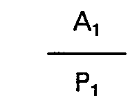

and this is indeed of the type
- This merging of the stages of Figs. 15 and 9 in one single stage is important because it ensures a perfect matching of the pole and zero at z=±1.
- Biquadratic stages T2 and T3 are of the type shown in Fig. 9 without damping capacitor ksC2. They have the respective transfer functions (see relation 15)


- Finally, biquadratic stage T'4 is of the type shown in Fig. 9 with damping capacitor k5C2 and cos to4=1 and having a transfer function (see relation 16)

- In Fig. 17, to be considered with the dotted connections but without the dashed line connections, the stages T"1, T2, T3 and T'4 may be identified in a relatively easy way with the stages of Figs. 15 and 9 (damped and with cos to1=1); Fig. 9 (undamped); Fig. 9 (undamped) and Fig. 9 (damped and with cos to4=1) respectively.
- The only problems might be the biquadratic stage T"1 and the leapfrog connections between the stages. Both are therefore explained in detail hereinafter.
- The stage of Figs. 15 and Fig. 9 only differ in the connection of their entries and therefore it was possible to use in Fig. 17 for T"1 a same circuit with an input IN, constituting the input of the filter and connected as in Fig. 15, and with another input A connected as in Fig. 9. However, because the signal at the input A should be positive (see Fig. 8) but is negative at the output OUT2 (see the transfer function of T2) to which A is coupled a negative capacitor -Ca corresponding to k4C2 in Fig. 9 has to be used.
- From 8 it also follows that OUT1 of T"1 and the output OUT3 of T3 are both connected to the input of T2 via a summing circuit S2. In Fig. 17 the output OUT1 is coupled to the inputs IN21 and IN22 of T2 via capacitors C8 and C9 corresponding to k3C1 and k4C2 in Fig. 9 and the output OUT3 is coupled to the same inputs IN21 and IN22 via capacitors C10 and C11 respectively also corresponding to k3C, and k4C2 in Fig. 9. The interconnections between the capacitors C8 and C10 as well as between the capacitors C2 and -Ca constitute summing point S1 in Fig. 8. From this figure it also follows that OUT2 of T2 and OUT of T'4 are both connected to the input of T3 via a summing circuit S3. In Fig. 17 output OUT2 is coupled to the inputs IN31 and IN32 of T3 via respective capacitors C14 and C15 corresponding to k3C, at k4C2 in Fig. 9 and the output OUT is coupled to the same inputs IN2, and IN22 via capacitors C16 and C17 corresponding to k3C1 and k4C2 in Fig. 9. The interconnections between the capacitors C14 and C16 as well as between the capacitors C15 and C17 constitute summing point S3 in Fig. 8. The output OUT3 of T3 is also connected to the input IN42 via negative capacitor -Cb. A negative capacitor -Cb is required because the signal at the output OUT3 of T3 is negative, as follows from the above given transfer function, whereas according to Fig. 8 the signal at the input of T'4 should be positive.
- As follows from the above the bandpass filter of Fig. 17 requires two negative capacitors -Ca and -Cb which do not exist. However, by manipulation of the charges on the various capacitors of the circuit these negative capacitors can be removed. Thus finally the filter circuit of Fig. 17 without the dotted connections, but with the dashed line connections is obtained i.e. with
- - capacitor C3 between OUT3 and IN,2;
- -capacitor C20 between OUT2 and IN42;
- - and capacitor C21 between the junction point of s111, s211 and s116, s216.
- This filter has a transfer function versus frequency characteristic such as shown in Fig. 4. Part of the corresponding attenuation versus frequency characteristic is also represented in Fig. 18. The group delay versus frequency characteristic of the filter is shown in Fig. 19 and fully satisfies the CCITT recommendations as indicated by the gauge.
- The receive lowpass filter RLPF of Fig. 1 is represented in detail in Fig. 20 and includes biquadratic stages T'1 and T'2 of the type shown in Fig. 9 (damped version) and Fig. 10 (damped version) respectively.
- In Fig. 20 capacitors C1 and C2 correspond to capacitors k3C1 and k4C2 in Fig. 9 and capacitors C8 and C9 correspond to capacitors k3C1 and k4C2 in Fig.10. The output OUT of T'2 is fed back to IN12 and IN22 of T'1 via connections including capacitors C3 and C4 respectively. Part of the attenuation versus frequency characteristic of the filter of Fig. 20 is shown in Fig. 21. In the lower passband the above mentioned

Claims (10)


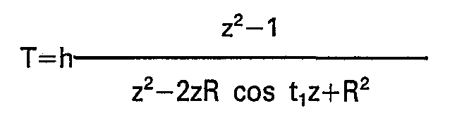
wherein
Applications Claiming Priority (2)
| Application Number | Priority Date | Filing Date | Title |
|---|---|---|---|
| BE2059738 | 1982-06-11 | ||
| BE2/59738A BE893486A (en) | 1982-06-11 | 1982-06-11 | Leap-frog filter with biquadratic stages - is formed by sampling filter with characteristics of coupled stages of given transfer function |
Publications (3)
| Publication Number | Publication Date |
|---|---|
| EP0096857A2 EP0096857A2 (en) | 1983-12-28 |
| EP0096857A3 EP0096857A3 (en) | 1985-12-11 |
| EP0096857B1 true EP0096857B1 (en) | 1990-01-31 |
Family
ID=3865602
Family Applications (1)
| Application Number | Title | Priority Date | Filing Date |
|---|---|---|---|
| EP19830105677 Expired EP0096857B1 (en) | 1982-06-11 | 1983-06-10 | Transmission filter with biquadratic filter stages |
Country Status (2)
| Country | Link |
|---|---|
| EP (1) | EP0096857B1 (en) |
| DE (1) | DE3381191D1 (en) |
Families Citing this family (2)
| Publication number | Priority date | Publication date | Assignee | Title |
|---|---|---|---|---|
| EP0874464A1 (en) * | 1997-04-21 | 1998-10-28 | Lsi Logic Corporation | Delta-sigma converter with low order anti-aliasing filter |
| EP1783897B1 (en) | 2005-11-08 | 2009-01-21 | Austriamicrosystems AG | Switched-capacitor amplifier arrangement and method |
-
1983
- 1983-06-10 DE DE8383105677T patent/DE3381191D1/en not_active Expired - Lifetime
- 1983-06-10 EP EP19830105677 patent/EP0096857B1/en not_active Expired
Also Published As
| Publication number | Publication date |
|---|---|
| EP0096857A3 (en) | 1985-12-11 |
| DE3381191D1 (en) | 1990-03-08 |
| EP0096857A2 (en) | 1983-12-28 |
Similar Documents
| Publication | Publication Date | Title |
|---|---|---|
| JPS6329849B2 (en) | ||
| SE454638B (en) | CIRCUIT TO AUTOMATICALLY DIGITAL SYNTHESIZE A CIRCUIT CUT IMPEDANCE WITH OUTPUT ADAPTATION | |
| CA1149479A (en) | Low sensitivity switched-capacitor ladder filter using monolithic mos chip | |
| US4181824A (en) | Balancing impedance circuit | |
| US4924189A (en) | Two-port switched capacitor filter netowrk with linearized phase/frequency response | |
| EP0455894B1 (en) | Impedance synthesis multiple loop using filtering means | |
| US4306197A (en) | Switched-capacitor elliptic filter | |
| EP0902535B1 (en) | Low-pass filter with a summing function | |
| US4174470A (en) | Electronic hybrid | |
| CA1233890A (en) | Decimating filter | |
| US4100515A (en) | Communication circuit having precision capacitor multiplier | |
| EP0096857A2 (en) | Transmission filter with biquadratic filter stages | |
| US5258713A (en) | Impedance generator for a telephone line interface circuit | |
| US4558185A (en) | Subscriber line interface circuit with complex impedance | |
| US4185250A (en) | Voice frequency RC active filter | |
| CA1169503A (en) | Driving point impedance derived from a transfer impedance | |
| US4223272A (en) | Four-terminal network of adjustable transfer function | |
| US6625278B1 (en) | Impedance matching with sigma delta filter | |
| US4296392A (en) | Switched capacitor bilinear resistors | |
| US4272735A (en) | Single amplifier variable gyrator | |
| US4281297A (en) | Electrical filter circuit utilizing charge transfer delay lines utilizing individual charge transfer delay elements | |
| US4245202A (en) | Floating gyrator having a current cancellation circuit | |
| US3056095A (en) | Ring modulator system | |
| EP0412560B1 (en) | Hybrid circuit | |
| US5249145A (en) | Transforming adaptors for wave digital filter and balancing network using same |
Legal Events
| Date | Code | Title | Description |
|---|---|---|---|
| PUAI | Public reference made under article 153(3) epc to a published international application that has entered the european phase |
Free format text: ORIGINAL CODE: 0009012 |
|
| AK | Designated contracting states |
Designated state(s): DE FR GB |
|
| PUAL | Search report despatched |
Free format text: ORIGINAL CODE: 0009013 |
|
| AK | Designated contracting states |
Designated state(s): DE FR GB |
|
| 17P | Request for examination filed |
Effective date: 19860124 |
|
| RAP1 | Party data changed (applicant data changed or rights of an application transferred) |
Owner name: ALCATEL N.V. |
|
| 17Q | First examination report despatched |
Effective date: 19880118 |
|
| RAP3 | Party data changed (applicant data changed or rights of an application transferred) |
Owner name: ALCATEL N.V. |
|
| GRAA | (expected) grant |
Free format text: ORIGINAL CODE: 0009210 |
|
| AK | Designated contracting states |
Kind code of ref document: B1 Designated state(s): DE FR GB |
|
| REF | Corresponds to: |
Ref document number: 3381191 Country of ref document: DE Date of ref document: 19900308 |
|
| ET | Fr: translation filed | ||
| PLBE | No opposition filed within time limit |
Free format text: ORIGINAL CODE: 0009261 |
|
| STAA | Information on the status of an ep patent application or granted ep patent |
Free format text: STATUS: NO OPPOSITION FILED WITHIN TIME LIMIT |
|
| 26N | No opposition filed | ||
| PGFP | Annual fee paid to national office [announced via postgrant information from national office to epo] |
Ref country code: GB Payment date: 19910528 Year of fee payment: 9 |
|
| PGFP | Annual fee paid to national office [announced via postgrant information from national office to epo] |
Ref country code: FR Payment date: 19910530 Year of fee payment: 9 |
|
| PG25 | Lapsed in a contracting state [announced via postgrant information from national office to epo] |
Ref country code: GB Effective date: 19920610 |
|
| GBPC | Gb: european patent ceased through non-payment of renewal fee |
Effective date: 19920610 |
|
| PG25 | Lapsed in a contracting state [announced via postgrant information from national office to epo] |
Ref country code: FR Effective date: 19930226 |
|
| REG | Reference to a national code |
Ref country code: FR Ref legal event code: ST |
|
| PGFP | Annual fee paid to national office [announced via postgrant information from national office to epo] |
Ref country code: DE Payment date: 19930821 Year of fee payment: 11 |
|
| PG25 | Lapsed in a contracting state [announced via postgrant information from national office to epo] |
Ref country code: DE Effective date: 19950301 |