EP0094410B1 - A method for comparison between a first optical signal and at least one other signal - Google Patents
A method for comparison between a first optical signal and at least one other signal Download PDFInfo
- Publication number
- EP0094410B1 EP0094410B1 EP82903490A EP82903490A EP0094410B1 EP 0094410 B1 EP0094410 B1 EP 0094410B1 EP 82903490 A EP82903490 A EP 82903490A EP 82903490 A EP82903490 A EP 82903490A EP 0094410 B1 EP0094410 B1 EP 0094410B1
- Authority
- EP
- European Patent Office
- Prior art keywords
- signal
- optical signal
- mis
- charge
- insulator
- Prior art date
- Legal status (The legal status is an assumption and is not a legal conclusion. Google has not performed a legal analysis and makes no representation as to the accuracy of the status listed.)
- Expired
Links
Images


Classifications
-
- G—PHYSICS
- G06—COMPUTING OR CALCULATING; COUNTING
- G06V—IMAGE OR VIDEO RECOGNITION OR UNDERSTANDING
- G06V10/00—Arrangements for image or video recognition or understanding
- G06V10/88—Image or video recognition using optical means, e.g. reference filters, holographic masks, frequency domain filters or spatial domain filters
Definitions
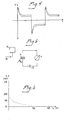
- the device comprises (Fig. 1) a MIS-structure consisting of a semiconductor 1 with a thin insulator layer 2, on which a thin electrically conducting layer 3 is applied.
- the energy band model for such a structure is shown in Fig. 2.
- the component in Fig. 2 is illuminated by chopped light from a chopper 10 and it is connected to an electric measuring instrument 4 in order to measure the current or the voltage as is shown in Fig. 3.
- the MIS-structure is indicated with 11. In the example reported here chopped light is thus used, which is easy to implement and makes the result easy to interpret.
- the intensity of the optical radiation varies as a function of time in another way or in the cases with several signals, that are mentioned below, if one of them varies as a function of time in such a way.
- the light in the present example which has an intensity ⁇ 1 and a photoenergy greater than the band gap of the semiconductor, gives rise to optically generated electrons and holes within the semiconductor.
- a condition for the good functioning of the component is that the energy band of the semiconductor bend at the surface. This can be controlled by introducing surface charges or by choosing the electrically conducting layer 3 in a suitably way. If the energy bands of the semiconductor are bent before the illumination in such a way that is shown in Fig.
- the electrons 5 created by the light will be accumulated in the energy well that exist in the semiconductor near its interface with the insulator.
- the holes 6, that are created during the illumination will drift into the bulk of the semiconductor and further out into an outer circuit through the metal contact 7 that is found on the backside of the component.
- a displacement of charge is thereby created, which can be measured as a current or a voltage with the instrument 4 in the outer circuit. This displacement of charge will continue until the bending of the energy band of the semiconductor near the insulator layer stops due to the neutralisation of charge that has been created by the illumination after a certain time. The length of this time is determined by the total RC-constant of the circuit shown in Fig. 3.
- Fig. 4 is an oscilloscope picture of the electric signal U(t) from a device according to Fig. 1-3.
- the amplitude of the signal U(t) in Fig. 4 is dependent upon the intensity ⁇ 1 and also upon the size ⁇ of the bending of the energy band in Fig. 2.
- ⁇ 1 the amplitude of the signal U(t) in Fig. 4 can therefore be varied by changing the surface potential 4 in Fig. 2.
- This change can be attained in two ways: By applying an outer voltage from a voltage source 12 between the contacts 3 and 7 or by illuminating the MIS-structure with an additional light source with constant light intensity ⁇ 2 (Fig. 5).
- Fig. 6 shows experimental data of the electric signal U as a function of an applied outer voltage V o during illumination with a chopped light source having the intensity ⁇ 1 .
- the essential information from Fig. 6 is that the signal U achieved by illuminating the MIS-structure with the chopped intensity ⁇ 1 can be controlled by the voltage V o .
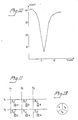
- Fig. 7 shows experimental data of how the electric signal U from the MIS-structure can be controlled by an additional light source with constant (non-chopped) intensity ⁇ 2.
- the extra light source gives rise to a reduction of the surface potential ⁇ (Fig. 2), which reduces U.
- the knee in the curve, that is found at ⁇ 2 ⁇ 15 depends upon energy states in the interface between the insulator and the semiconductor and has no qualitative effect on the function of the component. Such energy states can be affected by a thorough control of the manufacturing procedure during the application of the insulator layer on the semiconductor.
- Fig. 9 shows a slice in the form of a MIS-structure according to Fig. 1 seen from the side, on which the conductor 3 is applied.
- the time- dependent outsignal U is then only determined by ⁇ 1 as ⁇ 2 does not influence the surface potential ⁇ in the point that is illuminated with ⁇ 1 . If, however, the light spot with the intensity ⁇ 2 is moved in X-direction towards ⁇ 1 , the signal U will be influenced by ⁇ 2 as soon as the two light spots start to coincide.
- This signal has a minimum when ⁇ 1 and ⁇ 2 are identical and coincide.
- the above-mentioned device can therefore be used for image recognition.
- the dependence of the signal U on ⁇ 1 and ⁇ 2 can be varied by a suitable doping of the semiconductor and by introducing suitable energy states between the insulator 2 and the semiconductor 1.
- the other light signal can be chosen as a point shaped light source and be scanned in a raster pattern over the image. This makes it possible to have a serial reading of an image in the same way as in a television camera. By time differentiating the so created signal the image content can be differentiated in an arbitrary direction along the surface of the slice. By time integrating the signal in a corresponding way it is possible to carry out a line integration in the image. It is further possible to matrix multiply two images with each other by designing the MIS-structure in a suitable way.
- a processor having electric operator signals.
- the conductor 3 in Fig. 1 is then designed as a pattern of squares over the insulator surface in the way that is evident from Fig. 11.
- Each such conducting square 8 is addressed by x- and y- conductors via a MOS-transistor 9, integrated in the semiconductor slice.
- One example is to cross pairs of interconnected conductors, which pairs are insulated from all other pairs. In the crossing point between such pairs an area is created in which the surface potential ⁇ can be influenced. Such a crossing point can constitute an image point and can be addressed by applying a potential to the crossing conductor pairs.
- the colour information can be read from an image by scanning in a raster pattern according to section 3 if each image point is formed by several conducting layers 3 on top of the insulator 2, which layers are insulated from each other (see Fig. 12).
- the surface potential ⁇ will vary over the surface already before it is illuminated.
- One possibility is to make the MIS-structure as a so called FAMOS-structure, which means that a floating gate, a conducting material, is included in the insulator layer at the manufacture.
- the processor can then be programmed by applying a voltage over the FAMOS-structure at the same time as it is illuminated with an image containing the pattern with which one wishes to program the processor.
- the parts of the surface of the processor that are illuminated will then be charged, which will change the surface potential ⁇ there.
- Another possibility is to use the presence of movable charges in the insulator layer.
- a voltage across the MIS-structure raising its temperature to about 200°C and at the same time illuminate it with the desired operator image and movable charges, that are present in the insulator will be displaced more in brightly illuminated areas than in faintly illuminated areas. This gives rise to a varying surface potentiate (x, y), which is a copy of the operator image.
- a further possibility is to repopulate surface states and other states inside the oxide with different types of radiation: optical, X-ray and particle radiation.
Landscapes
- Engineering & Computer Science (AREA)
- General Physics & Mathematics (AREA)
- Multimedia (AREA)
- Theoretical Computer Science (AREA)
- Physics & Mathematics (AREA)
- Solid State Image Pick-Up Elements (AREA)
- Optical Communication System (AREA)
- Photoreceptors In Electrophotography (AREA)
- Transforming Light Signals Into Electric Signals (AREA)
- Character Input (AREA)
- Amplifiers (AREA)
- Networks Using Active Elements (AREA)
- Electrotherapy Devices (AREA)
- Optical Head (AREA)
- Image Input (AREA)
- Wrapping Of Specific Fragile Articles (AREA)
- Inspection Of Paper Currency And Valuable Securities (AREA)
- Light Guides In General And Applications Therefor (AREA)
- Testing Of Optical Devices Or Fibers (AREA)
- Photometry And Measurement Of Optical Pulse Characteristics (AREA)
- Character Discrimination (AREA)
- Image Analysis (AREA)
- Testing Or Measuring Of Semiconductors Or The Like (AREA)
Abstract
Description
- The present invention relates to a method for comparison between a first optical signal and at least one other signal.
- The predominant technique today for processing optical information in the form of images is to process the content of the image point by point. One often uses an image sensor of the charge transfer device type, from which the image information is fed out point by point and stored in a memory. The content of this memory is then processed bit by bit against information stored in an operator memory. In this way operations of the type correlation, derivation etc in order to recognize images or different kinds of transformations of matrices for bandwidth-limitation of the content of the images is performed. As this method means a serial processing of a very large amount of information the image processing becomes time consuming and it demands a very high computer capacity.
- During the last years there have been a great international activity in order to create methods performing parallel processing of the content of an image. This means that all image points are processed simultaneously, which gives tremendous benefits in calculation time. One has then mostly used the possibility for Fourier-transformation, which the nature offers when coherent light is used. Such methods demand a very high mechanical stability in the optical system, that is used for processing the image.
- The invention that will be described here, has at least four advantages compared with previous solutions for processing images:
- (i) It is based on a very simple sensor structure (ii) It can perform parallel processing
- (iii) It uses incoherent light
- (iv) An image can be processed with optical signals, electric signals or a combination of these. The operator signals can either be addressed to discrete image points or operate parallelly over the image or parts of it.
- The mentioned advantages is achieved by giving the invention the design that is evident from the following claims.
- In the following the invention will be further described with reference to the attached drawings, in 'which
- Fig. 1 shows a cross-section of the MIS-structure
- Fig. 2 shows the energy band model for a structure according to Fig. 1 illuminated by chopped light
- Fig. 3 shows the structure in Fig. 1 and 2 connected to a measuring instrument
- Fig. 4 shows an oscilloscope picture from a device according to Fig. 1-3
- Fig. 5 shows the structure illuminated both with chopped light and constant light
- Fig. 6 shows experimental data of the electric signal U as a function of an applied outer potential V. during illumination with a chopped light source with the. intensity φ1
- Fig. 7 shows experimental data of how the electric signal U from the MIS-structure can be controlled by another light source with constant intensity Φ2
- Fig. 8 shows experimental data of the electric signal U as a function of the chopped light source with the intensity (Dl, with the intensity Φ2 from the constant light source as a parameter
- Fig. 9 shows a slice, in the form of a MIS-structure according to Fig. 1 seen from the side on which the
conductor 3 is applied, illuminated in one point by chopped light with the intensity φ1 and in another point by constant light with the intensity Φ2 - Fig. 10 shows the electric signal U as a function of the displacement of the light spot with the intensity Φ2 in Fig. 9
- Fig. 11 shows how different image points in an opto-electric processor can be addressed
- Fig. 12 shows how an image point in a colour sensitive optical processor can be designed.
- The device comprises (Fig. 1) a MIS-structure consisting of a
semiconductor 1 with athin insulator layer 2, on which a thin electrically conductinglayer 3 is applied. The energy band model for such a structure is shown in Fig. 2. The component in Fig. 2 is illuminated by chopped light from achopper 10 and it is connected to an electric measuring instrument 4 in order to measure the current or the voltage as is shown in Fig. 3. The MIS-structure is indicated with 11. In the example reported here chopped light is thus used, which is easy to implement and makes the result easy to interpret. It must however be emphasized that it means no difference in principle if the intensity of the optical radiation varies as a function of time in another way or in the cases with several signals, that are mentioned below, if one of them varies as a function of time in such a way. The light in the present example, which has an intensity φ1 and a photoenergy greater than the band gap of the semiconductor, gives rise to optically generated electrons and holes within the semiconductor. A condition for the good functioning of the component is that the energy band of the semiconductor bend at the surface. This can be controlled by introducing surface charges or by choosing the electrically conductinglayer 3 in a suitably way. If the energy bands of the semiconductor are bent before the illumination in such a way that is shown in Fig. 2, theelectrons 5 created by the light will be accumulated in the energy well that exist in the semiconductor near its interface with the insulator. Theholes 6, that are created during the illumination, will drift into the bulk of the semiconductor and further out into an outer circuit through the metal contact 7 that is found on the backside of the component. A displacement of charge is thereby created, which can be measured as a current or a voltage with the instrument 4 in the outer circuit. This displacement of charge will continue until the bending of the energy band of the semiconductor near the insulator layer stops due to the neutralisation of charge that has been created by the illumination after a certain time. The length of this time is determined by the total RC-constant of the circuit shown in Fig. 3. If the RC-constant is long compared with the chopping frequency, one gets such a signal in the outer circuit as is shown in Fig. 4, which is an oscilloscope picture of the electric signal U(t) from a device according to Fig. 1-3. The amplitude of the signal U(t) in Fig. 4 is dependent upon the intensity φ1 and also upon the size ψ of the bending of the energy band in Fig. 2. For a certain intensity φ1 the amplitude of the signal U(t) in Fig. 4 can therefore be varied by changing the surface potential 4 in Fig. 2. This change can be attained in two ways: By applying an outer voltage from avoltage source 12 between thecontacts 3 and 7 or by illuminating the MIS-structure with an additional light source with constant light intensity Φ2 (Fig. 5). - Fig. 6 shows experimental data of the electric signal U as a function of an applied outer voltage Vo during illumination with a chopped light source having the intensity φ1. The essential information from Fig. 6 is that the signal U achieved by illuminating the MIS-structure with the chopped intensity φ1 can be controlled by the voltage Vo.
- Fig. 7 shows experimental data of how the electric signal U from the MIS-structure can be controlled by an additional light source with constant (non-chopped) intensity Φ2. The extra light source gives rise to a reduction of the surface potential ψ (Fig. 2), which reduces U. In Fig. 7 one can see that for φ2≲10 and φ2≳20 U=f(Φ2) is a nearly hyperbolic function. The knee in the curve, that is found at φ2≈15 depends upon energy states in the interface between the insulator and the semiconductor and has no qualitative effect on the function of the component. Such energy states can be affected by a thorough control of the manufacturing procedure during the application of the insulator layer on the semiconductor.
- That the signal U is also a function of the chopped intensity φ1 is shown in Fig. 8, which represents experimental data of U=f(φ1) with φ2 as a parameter.
- We have now shown with theoretical arguments and experimental data how the optically induced electric signal from a MIS-structure can be controlled by another optical signal Φ2. It is therefore possible to write

- Fig. 9 shows a slice in the form of a MIS-structure according to Fig. 1 seen from the side, on which the
conductor 3 is applied. We imagine a system of co-ordinates (x, y) in the plane of the slice and illuminate the slice in two different points, with the chopped intensity φ1 and also with the constant intensity Φ2. The time- dependent outsignal U is then only determined by φ1 as φ2 does not influence the surface potential ψ in the point that is illuminated with φ1. If, however, the light spot with the intensity Φ2 is moved in X-direction towards φ1, the signal U will be influenced by Φ2 as soon as the two light spots start to coincide. An experiment verifying this is shown in Fig. 10, in which the signal U is measured as a function of the displacement of the light spot with the intensity φ2 in Fig. 9. The two light spots coincide completely when X=6.0, which is the point in which U has a minimum. - Now it is easy to generalize this reasoning so that it is valid for two images described by the functions φ1(x, y) and φ2(x, y). If the image φ1(x, y) is chopped in the same way as previously the light spot φ1, one will get a charge displacement in every point (x, y) in the surface of the MIS-structure which will add up to a signal U in the outer circuit. We saw previously (Fig. 7 and 8) that U is approximately reciprocally proportional to φ2 and approximately proportional to φ1. For two images the signal is an expression of the type

- This signal has a minimum when φ1 and φ2 are identical and coincide. The above-mentioned device can therefore be used for image recognition. The dependence of the signal U on φ1 and φ2, as it is described in Fig. 7 and 8, can be varied by a suitable doping of the semiconductor and by introducing suitable energy states between the
insulator 2 and thesemiconductor 1. - In order to improve the lateral resolution during the correlation of two images one can see to that the energy well for electrons or holes, that exists at the interface between the insulator and the semiconductor is limited in lateral direction. The surface is then provided with a large number of such laterally limited energy wells, each of which constituting an image point. This prevents the electrons and holes at the surface to spread out over a larger area, which increases the lateral resolution. Another way to improve the resolution is to limit the mobility of the charge carriers in the energy well. A lateral limitation of the energy wells and a reduction of the mobility is achieved by introducing surface charge, selecting in a suitable way the doping or the material in the
conductor 3. - If any of φ1 and φ2 is chosen as an image, the other light signal can be chosen as a point shaped light source and be scanned in a raster pattern over the image. This makes it possible to have a serial reading of an image in the same way as in a television camera. By time differentiating the so created signal the image content can be differentiated in an arbitrary direction along the surface of the slice. By time integrating the signal in a corresponding way it is possible to carry out a line integration in the image. It is further possible to matrix multiply two images with each other by designing the MIS-structure in a suitable way.
- By using the characteristic of the MIS-structure, described in connection with Fig. 6, namely that the signal U can be controlled by an outer voltage Vo, it is possible to make a processor, having electric operator signals. The
conductor 3 in Fig. 1 is then designed as a pattern of squares over the insulator surface in the way that is evident from Fig. 11. Each such conductingsquare 8 is addressed by x- and y- conductors via a MOS-transistor 9, integrated in the semiconductor slice. With this structure it is possible to operate on an image with optical signals in the way described insection 3 and also with electric signals so that parts of an image can be selected with the possibilities of addressing described in Fig. 11. - There is also other possibilities of electric processing. One example is to cross pairs of interconnected conductors, which pairs are insulated from all other pairs. In the crossing point between such pairs an area is created in which the surface potential ψ can be influenced. Such a crossing point can constitute an image point and can be addressed by applying a potential to the crossing conductor pairs.
- The colour information can be read from an image by scanning in a raster pattern according to
section 3 if each image point is formed by several conductinglayers 3 on top of theinsulator 2, which layers are insulated from each other (see Fig. 12). - Each part of the image point is in addition to the conducting material also provided with an optical band-pass filter with a typical passwavelength for each part of the image point. Each part of the image point is then modulated by an electric alternating voltage signal Vo with a characteristic frequency fr, fg, fb etc for each part of the image point. The colour information in an image is obtained by band-pass filtering the electric outsignal U at the frequencies fr, fg, fb etc.
- By introducing over the surface of the MIS-structure a varying surface charge, the surface potential ψ will vary over the surface already before it is illuminated. This means a possibility to provide the processor with read only programming. There are several possibilities to introduce such a varying surface potential. One possibility is to make the MIS-structure as a so called FAMOS-structure, which means that a floating gate, a conducting material, is included in the insulator layer at the manufacture. The processor can then be programmed by applying a voltage over the FAMOS-structure at the same time as it is illuminated with an image containing the pattern with which one wishes to program the processor. The parts of the surface of the processor that are illuminated will then be charged, which will change the surface potential ψ there.
- Another possibility is to use the presence of movable charges in the insulator layer. By applying a voltage across the MIS-structure, raising its temperature to about 200°C and at the same time illuminate it with the desired operator image and movable charges, that are present in the insulator will be displaced more in brightly illuminated areas than in faintly illuminated areas. This gives rise to a varying surface potentiate (x, y), which is a copy of the operator image.
- A further possibility is to use semiconductor lithographic methods in combination with ion implantation. The operator image is then established in the lithographic process and an ion implanted pattern is achieved which gives a varying charge in the insulator-semiconductor interface.
- A further possibility is to repopulate surface states and other states inside the oxide with different types of radiation: optical, X-ray and particle radiation.
Claims (16)
Priority Applications (1)
| Application Number | Priority Date | Filing Date | Title |
|---|---|---|---|
| AT82903490T ATE28006T1 (en) | 1981-11-23 | 1982-11-19 | METHOD OF COMPARISON BETWEEN A FIRST OPTICAL SIGNAL AND AT LEAST ONE OTHER SIGNAL. |
Applications Claiming Priority (2)
| Application Number | Priority Date | Filing Date | Title |
|---|---|---|---|
| SE8106927 | 1981-11-23 | ||
| SE8106927A SE442152B (en) | 1981-11-23 | 1981-11-23 | PROCEDURE FOR COMPARISON OF A FIRST OPTICAL SIGNAL WITH AT LEAST ANOTHER SIGNAL |
Publications (2)
| Publication Number | Publication Date |
|---|---|
| EP0094410A1 EP0094410A1 (en) | 1983-11-23 |
| EP0094410B1 true EP0094410B1 (en) | 1987-06-24 |
Family
ID=20345082
Family Applications (1)
| Application Number | Title | Priority Date | Filing Date |
|---|---|---|---|
| EP82903490A Expired EP0094410B1 (en) | 1981-11-23 | 1982-11-19 | A method for comparison between a first optical signal and at least one other signal |
Country Status (10)
| Country | Link |
|---|---|
| US (1) | US4651014A (en) |
| EP (1) | EP0094410B1 (en) |
| JP (1) | JPS58502023A (en) |
| AT (1) | ATE28006T1 (en) |
| DE (1) | DE3276646D1 (en) |
| DK (1) | DK338483A (en) |
| FI (1) | FI78365C (en) |
| NO (1) | NO160678C (en) |
| SE (1) | SE442152B (en) |
| WO (1) | WO1983001852A1 (en) |
Cited By (1)
| Publication number | Priority date | Publication date | Assignee | Title |
|---|---|---|---|---|
| RU2451978C1 (en) * | 2011-05-20 | 2012-05-27 | Михаил Александрович Аллес | Optical minimum signal nanoselector |
Families Citing this family (2)
| Publication number | Priority date | Publication date | Assignee | Title |
|---|---|---|---|---|
| DE3925947A1 (en) * | 1989-08-05 | 1991-02-07 | Licentia Gmbh | CORRELATOR |
| US5780112A (en) * | 1996-05-15 | 1998-07-14 | Lrc Products, Ltd. | Power-free latex articles and methods of making the same |
Family Cites Families (6)
| Publication number | Priority date | Publication date | Assignee | Title |
|---|---|---|---|---|
| US3916268A (en) * | 1969-01-21 | 1975-10-28 | Gen Electric | Device for storing information and providing an electric readout from a conductor-insulator-semiconductor structure |
| GB1444543A (en) * | 1972-09-22 | 1976-08-04 | Mullard Ltd | Solid state image display and/or conversion device |
| DE2345686A1 (en) * | 1972-09-22 | 1974-04-04 | Philips Nv | IMAGE REPLAY AND / OR CONVERSION DEVICE |
| NL180157C (en) * | 1975-06-09 | 1987-01-02 | Philips Nv | SEMICONDUCTOR IMAGE RECORDING DEVICE. |
| US4539591A (en) * | 1979-03-22 | 1985-09-03 | University Of Texas System | Method of impressing and reading out a surface charge on a multi-layered detector structure |
| DE2939403A1 (en) * | 1979-09-28 | 1981-04-16 | Siemens AG, 1000 Berlin und 8000 München | MONOLITHICALLY INTEGRATED CIRCUIT FOR LINE SCREENING |
-
1981
- 1981-11-23 SE SE8106927A patent/SE442152B/en not_active IP Right Cessation
-
1982
- 1982-11-19 JP JP82503455A patent/JPS58502023A/en active Pending
- 1982-11-19 AT AT82903490T patent/ATE28006T1/en not_active IP Right Cessation
- 1982-11-19 US US06/525,045 patent/US4651014A/en not_active Expired - Fee Related
- 1982-11-19 EP EP82903490A patent/EP0094410B1/en not_active Expired
- 1982-11-19 DE DE8282903490T patent/DE3276646D1/en not_active Expired
- 1982-11-19 WO PCT/SE1982/000390 patent/WO1983001852A1/en not_active Ceased
-
1983
- 1983-07-12 FI FI832539A patent/FI78365C/en not_active IP Right Cessation
- 1983-07-15 NO NO83832578A patent/NO160678C/en unknown
- 1983-07-22 DK DK338483A patent/DK338483A/en not_active Application Discontinuation
Cited By (1)
| Publication number | Priority date | Publication date | Assignee | Title |
|---|---|---|---|---|
| RU2451978C1 (en) * | 2011-05-20 | 2012-05-27 | Михаил Александрович Аллес | Optical minimum signal nanoselector |
Also Published As
| Publication number | Publication date |
|---|---|
| FI832539L (en) | 1983-07-12 |
| SE442152B (en) | 1985-12-02 |
| FI832539A0 (en) | 1983-07-12 |
| FI78365C (en) | 1989-07-10 |
| NO160678B (en) | 1989-02-06 |
| NO160678C (en) | 1989-05-16 |
| US4651014A (en) | 1987-03-17 |
| JPS58502023A (en) | 1983-11-24 |
| WO1983001852A1 (en) | 1983-05-26 |
| NO832578L (en) | 1983-07-15 |
| DE3276646D1 (en) | 1987-07-30 |
| FI78365B (en) | 1989-03-31 |
| EP0094410A1 (en) | 1983-11-23 |
| ATE28006T1 (en) | 1987-07-15 |
| DK338483D0 (en) | 1983-07-22 |
| DK338483A (en) | 1983-07-22 |
| SE8106927L (en) | 1983-05-24 |
Similar Documents
| Publication | Publication Date | Title |
|---|---|---|
| DE69811361T2 (en) | FINGERPRINT SENSOR WITH AN ANISOTROPIC DIELECTRIC LAYER AND RELATED METHOD | |
| DE69809907T2 (en) | FINGERPRINT SENSOR WITH GAIN CONTROL FEATURES AND RELATED METHODS | |
| DE69813211T2 (en) | FINGERPRINT SENSOR WITH FILTERING AND ENERGY SAVING PROPERTIES AND RELATED METHODS | |
| EP0040836A1 (en) | Detector for fingerprints and method of enhancing them | |
| DE69820551T2 (en) | Electrostatic discharge protection for a capacitive fingerprint sensing matrix | |
| US4780604A (en) | IC-incorporated memory card | |
| US4375652A (en) | High-speed time delay and integration solid state scanner | |
| US4651014A (en) | Method for comparison between a first optical signal and at least one other signal | |
| DE4035396C2 (en) | ||
| EP0221657A1 (en) | Charged-particle-beam lithography | |
| EP0176745A1 (en) | Device and method to measure lengths in a scanning corpuscular microscope | |
| DE3406268C2 (en) | Image reader | |
| DE2007728C3 (en) | Method and device for evaluating the distribution of the electrical charge on an electrostatically charged layer | |
| DE3509710C2 (en) | Electrostatic voltmeter | |
| SU1081619A1 (en) | Method of producing raster electrographic photo medium | |
| CN1344001A (en) | Ferroelectric emitter body | |
| DE1549144B2 (en) | Information storage device and method for storing information using the same | |
| DE2460715B2 (en) | Corpuscular beam optical device for corpuscle irradiation of a specimen in the form of a surface pattern with several surface elements that are identical to one another | |
| FR2438909A1 (en) | TARGET FOR SCANNING MEMORY TUBES AND METHOD FOR DELETING INFORMATION | |
| SU989531A1 (en) | Method of recording information on relief-graphic carrier | |
| GB2633461A (en) | Deploying electric fields | |
| JPH11224634A (en) | Scanning image forming method and scanning image forming apparatus | |
| JPS5971033A (en) | Optical recorder | |
| SU1282241A1 (en) | Spatial-frequency filter of one-dimensional optical signal | |
| Kin et al. | Multiwavelength feature detection and recognition |
Legal Events
| Date | Code | Title | Description |
|---|---|---|---|
| PUAI | Public reference made under article 153(3) epc to a published international application that has entered the european phase |
Free format text: ORIGINAL CODE: 0009012 |
|
| 17P | Request for examination filed |
Effective date: 19830721 |
|
| AK | Designated contracting states |
Designated state(s): AT BE CH DE FR GB LI LU NL |
|
| GRAA | (expected) grant |
Free format text: ORIGINAL CODE: 0009210 |
|
| AK | Designated contracting states |
Kind code of ref document: B1 Designated state(s): AT BE CH DE FR GB LI LU NL |
|
| REF | Corresponds to: |
Ref document number: 28006 Country of ref document: AT Date of ref document: 19870715 Kind code of ref document: T |
|
| REF | Corresponds to: |
Ref document number: 3276646 Country of ref document: DE Date of ref document: 19870730 |
|
| ET | Fr: translation filed | ||
| PG25 | Lapsed in a contracting state [announced via postgrant information from national office to epo] |
Ref country code: LU Free format text: LAPSE BECAUSE OF NON-PAYMENT OF DUE FEES Effective date: 19871130 |
|
| PLBE | No opposition filed within time limit |
Free format text: ORIGINAL CODE: 0009261 |
|
| STAA | Information on the status of an ep patent application or granted ep patent |
Free format text: STATUS: NO OPPOSITION FILED WITHIN TIME LIMIT |
|
| 26N | No opposition filed | ||
| PGFP | Annual fee paid to national office [announced via postgrant information from national office to epo] |
Ref country code: AT Payment date: 19891130 Year of fee payment: 8 |
|
| PGFP | Annual fee paid to national office [announced via postgrant information from national office to epo] |
Ref country code: BE Payment date: 19891204 Year of fee payment: 8 |
|
| PGFP | Annual fee paid to national office [announced via postgrant information from national office to epo] |
Ref country code: LU Payment date: 19891229 Year of fee payment: 8 |
|
| PG25 | Lapsed in a contracting state [announced via postgrant information from national office to epo] |
Ref country code: AT Effective date: 19901119 |
|
| PG25 | Lapsed in a contracting state [announced via postgrant information from national office to epo] |
Ref country code: BE Effective date: 19901130 |
|
| BERE | Be: lapsed |
Owner name: FORSVARETS FORSKNINGSANSTALT Effective date: 19901130 |
|
| PGFP | Annual fee paid to national office [announced via postgrant information from national office to epo] |
Ref country code: GB Payment date: 19931012 Year of fee payment: 12 |
|
| PGFP | Annual fee paid to national office [announced via postgrant information from national office to epo] |
Ref country code: CH Payment date: 19931013 Year of fee payment: 12 |
|
| PGFP | Annual fee paid to national office [announced via postgrant information from national office to epo] |
Ref country code: DE Payment date: 19931102 Year of fee payment: 12 |
|
| PGFP | Annual fee paid to national office [announced via postgrant information from national office to epo] |
Ref country code: NL Payment date: 19931130 Year of fee payment: 12 Ref country code: FR Payment date: 19931130 Year of fee payment: 12 |
|
| PG25 | Lapsed in a contracting state [announced via postgrant information from national office to epo] |
Ref country code: GB Effective date: 19941119 |
|
| PG25 | Lapsed in a contracting state [announced via postgrant information from national office to epo] |
Ref country code: LI Effective date: 19941130 Ref country code: CH Effective date: 19941130 |
|
| PG25 | Lapsed in a contracting state [announced via postgrant information from national office to epo] |
Ref country code: NL Effective date: 19950601 |
|
| NLV4 | Nl: lapsed or anulled due to non-payment of the annual fee | ||
| GBPC | Gb: european patent ceased through non-payment of renewal fee |
Effective date: 19941119 |
|
| PG25 | Lapsed in a contracting state [announced via postgrant information from national office to epo] |
Ref country code: FR Effective date: 19950731 |
|
| REG | Reference to a national code |
Ref country code: CH Ref legal event code: PL |
|
| PG25 | Lapsed in a contracting state [announced via postgrant information from national office to epo] |
Ref country code: DE Effective date: 19950801 |
|
| REG | Reference to a national code |
Ref country code: FR Ref legal event code: ST |