EP0092330B1 - Infra red photo detector systems - Google Patents
Infra red photo detector systems Download PDFInfo
- Publication number
- EP0092330B1 EP0092330B1 EP83301817A EP83301817A EP0092330B1 EP 0092330 B1 EP0092330 B1 EP 0092330B1 EP 83301817 A EP83301817 A EP 83301817A EP 83301817 A EP83301817 A EP 83301817A EP 0092330 B1 EP0092330 B1 EP 0092330B1
- Authority
- EP
- European Patent Office
- Prior art keywords
- bias
- light source
- infra red
- electrodes
- image position
- Prior art date
- Legal status (The legal status is an assumption and is not a legal conclusion. Google has not performed a legal analysis and makes no representation as to the accuracy of the status listed.)
- Expired - Lifetime
Links
- 238000000034 method Methods 0.000 claims description 17
- 238000003384 imaging method Methods 0.000 claims description 5
- 229910000673 Indium arsenide Inorganic materials 0.000 claims description 2
- WPYVAWXEWQSOGY-UHFFFAOYSA-N indium antimonide Chemical compound [Sb]#[In] WPYVAWXEWQSOGY-UHFFFAOYSA-N 0.000 claims description 2
- RPQDHPTXJYYUPQ-UHFFFAOYSA-N indium arsenide Chemical compound [In]#[As] RPQDHPTXJYYUPQ-UHFFFAOYSA-N 0.000 claims description 2
- 238000003331 infrared imaging Methods 0.000 claims description 2
- 238000005286 illumination Methods 0.000 description 14
- 239000000969 carrier Substances 0.000 description 10
- 239000000758 substrate Substances 0.000 description 10
- 230000005855 radiation Effects 0.000 description 9
- 239000000463 material Substances 0.000 description 8
- 230000004044 response Effects 0.000 description 7
- IJGRMHOSHXDMSA-UHFFFAOYSA-N Atomic nitrogen Chemical compound N#N IJGRMHOSHXDMSA-UHFFFAOYSA-N 0.000 description 4
- 239000004065 semiconductor Substances 0.000 description 4
- 230000035945 sensitivity Effects 0.000 description 4
- 230000000694 effects Effects 0.000 description 3
- NJPPVKZQTLUDBO-UHFFFAOYSA-N novaluron Chemical compound C1=C(Cl)C(OC(F)(F)C(OC(F)(F)F)F)=CC=C1NC(=O)NC(=O)C1=C(F)C=CC=C1F NJPPVKZQTLUDBO-UHFFFAOYSA-N 0.000 description 3
- 238000009792 diffusion process Methods 0.000 description 2
- 230000006870 function Effects 0.000 description 2
- 239000012535 impurity Substances 0.000 description 2
- 230000010354 integration Effects 0.000 description 2
- 239000007788 liquid Substances 0.000 description 2
- 238000005259 measurement Methods 0.000 description 2
- 229910052757 nitrogen Inorganic materials 0.000 description 2
- 238000010408 sweeping Methods 0.000 description 2
- 206010028980 Neoplasm Diseases 0.000 description 1
- XUIMIQQOPSSXEZ-UHFFFAOYSA-N Silicon Chemical compound [Si] XUIMIQQOPSSXEZ-UHFFFAOYSA-N 0.000 description 1
- 238000009825 accumulation Methods 0.000 description 1
- 230000003321 amplification Effects 0.000 description 1
- 238000003491 array Methods 0.000 description 1
- 238000012937 correction Methods 0.000 description 1
- 238000001514 detection method Methods 0.000 description 1
- 238000010586 diagram Methods 0.000 description 1
- 229910052732 germanium Inorganic materials 0.000 description 1
- GNPVGFCGXDBREM-UHFFFAOYSA-N germanium atom Chemical compound [Ge] GNPVGFCGXDBREM-UHFFFAOYSA-N 0.000 description 1
- 238000002347 injection Methods 0.000 description 1
- 239000007924 injection Substances 0.000 description 1
- 238000012544 monitoring process Methods 0.000 description 1
- 230000007935 neutral effect Effects 0.000 description 1
- 238000003199 nucleic acid amplification method Methods 0.000 description 1
- 230000000737 periodic effect Effects 0.000 description 1
- 229910052710 silicon Inorganic materials 0.000 description 1
- 239000010703 silicon Substances 0.000 description 1
- 229910002058 ternary alloy Inorganic materials 0.000 description 1
Images


Classifications
-
- H—ELECTRICITY
- H10—SEMICONDUCTOR DEVICES; ELECTRIC SOLID-STATE DEVICES NOT OTHERWISE PROVIDED FOR
- H10F—INORGANIC SEMICONDUCTOR DEVICES SENSITIVE TO INFRARED RADIATION, LIGHT, ELECTROMAGNETIC RADIATION OF SHORTER WAVELENGTH OR CORPUSCULAR RADIATION
- H10F30/00—Individual radiation-sensitive semiconductor devices in which radiation controls the flow of current through the devices, e.g. photodetectors
- H10F30/10—Individual radiation-sensitive semiconductor devices in which radiation controls the flow of current through the devices, e.g. photodetectors the devices being sensitive to infrared radiation, visible or ultraviolet radiation, and having no potential barriers, e.g. photoresistors
-
- G—PHYSICS
- G01—MEASURING; TESTING
- G01B—MEASURING LENGTH, THICKNESS OR SIMILAR LINEAR DIMENSIONS; MEASURING ANGLES; MEASURING AREAS; MEASURING IRREGULARITIES OF SURFACES OR CONTOURS
- G01B11/00—Measuring arrangements characterised by the use of optical techniques
Definitions
- This invention relates to infra red (I.R.) photo detector systems, using detectors that change their resistivity when illuminated by infra red radiation.
- I.R. infra red
- Photo detectors are used in a variety of infra red detection systems. For example burglar alarms where the body heat, of a person passing through a door, is focussed onto an infra red detector. The change in resistivity of the detector causes an alarm signal. Such a system senses only the near presence of a person or other hot object such as a fire. More elaborate systems may use an array of detectors to give an approximate position or direction of a hot object in accordance with the particular detector illuminated. Such systems are often termed staring arrays. The positional accuracy for determining hot objects is limited by the number and size of detectors. Using very large numbers of small detectors a reasonable image of a thermal scene is theoretically obtainable. However each detector is only capable of providing a signal representing average radiation received. It cannot distinguish between overall illumination and point illumination. Resolution is thus limited by detector size.
- the detector output may be viewed via a television monitor and is observed in detail similar to that from conventional television cameras. These systems give sufficient detail for example to detect human tumours by the temperature difference between healthy and tumerous tissues. The high performance is unnecessarily good for some applications, also the cost and mechanical complexity is high.
- infra red detector is disclosed in US Pat. No. 3,995,159, and a variant of this is disclosed in GB 2,019,649A. These relate to an integrating strip detector.
- a detector incorporates an elongate strip of infra red photoconductive material having a respective electrical bias contact at each end.
- Imaging means are provided to form an image of a thermal scene on the strip surface. Photocarriers produced by the image are swept along the length of the strip in a direction parallel to the surface on which the image is formed. The photocarriers are swept towards the output bias contact under the action of voltage applied across both bias contacts. Scanning means are employed to scan the image along the strip in the same direction and at the same rate as the photocarrier flow.
- each image element continues to produce photocarriers to augment those it produced earlier.
- imaging scanning and photocarrier drift must remain matched in magnitude and direction to ensure that dissimilar image elements do not contribute to like signal portions.
- the output signal from the strip is taken across a readout contact and the output bias contact, the readout contact being positioned close to the output contact and the strip length therebetween defining a readout region.
- the detected image may be measured as a bulk resistivity change in the readout region. Since photocarriers generated in the strip must flow towards the readout region, the strip is electrically unidirectional.
- infra red detector A further form of infra red detector is disclosed in US Pat. No. 4,004,148. It relates to an accumulation mode charge injection infra red sensor, i.e. a capacitive device. It comprises a silicon semiconductor substrate one surface of which bears thin insulating oxide layer (Si0 2 ). Electrical contacts are applied to the insulating layer and to the remote surface of the substrate. Consequently, the contacts are spaced by the combined substrate and layer thicknesses. The contacts are connected to a source of bi-directional pulses. Infra red light illuminates and is dispersed over the substrate surface, the light passing through the substrate's electrical contact which is transparent. The detector is operated at cryogenic temperatures (5-50 K) so that impurity states in the semiconductor substrate are neutral (un-ionised).
- cryogenic temperatures 5-50 K
- a source of bi-directional electrical pulses is connected across the two contacts, ie. across the contact to the insulating oxide layer and the transparent contact to semiconductor substrate.
- a first pulse polarity drives charge created by illumination to the interface between the insulating layer and the semiconductor substrate. Charge therefore accumulates at this interface.
- the reverse polarity drives the accumulated charge to the transparent contact of the substrate for subsequent integration and amplification in an external circuit. Movement of charge is generally parallel to the thickness dimensions of the substrate and insulating layers, ie perpendicular to the plane of the infra red-illuminated surface of the transparent contact.
- a difference in output signal level from the external circuit for the two pulse polarities provides a measure of infra red illumination.
- the present invention provides greater image position information than is obtainable from known staring systems, and has reduced complexity as compared to known mechanical scanning systems.
- the present invention provides a method of detecting the position of an infra red light source in a scene, the method including the steps of:
- the electrical bias may be DC and varied by polarity reversal.
- the image position may then be obtained from a difference/sum ratio of element resistances for the two bias polarities.
- the bias may be AC with high frequency polarity reversal, the image position being detected by asymmetry in the element output signal arising from resistance variation with bias polarity.
- the asymmetry may be an offset asymmetry detected in magnitude and sign, and may be processed to provide an offset- counteracting DC bias feedback signal itself indicating image position.
- the electrical bias signal is DC
- the image is scanned in a direction opposite to photocarrier flow and the image position is extracted from the time interval between a scan synchronisation pulse and receipt of an edge of a ramp signal output from the photoconductive element.
- the scan may be in a saw-tooth manner.
- the photoconductive element material may be Cd x Hg 1-x Te, InSb or InAs, and the element may be cooled.
- the invention also provides detector apparatus for performing the foregoing method, the apparatus including:
- the bias reversing means may be arranged to operate at high frequency.
- the imaged light source position may be moved by means. adapted to cause it to precess or wobble on the element surface region.
- the photoconductive element may have a plurality of opposed pairs of bias electrodes regularly spaced around the photosensitive region and biasing means for biasing successive electrode pairs. Such an element is employed either with bias reversing means or with image movement means and means for indicating image position from element resistance change in response to bias reversal or image movement.
- a detector system 1 comprises a piece of infra red detector material 2 such as the ternary alloy Cd x Hg,_ x Te. Typical dimensions are 100 pm 2.
- Strip electrodes 3, 4 are attached along two opposite edges of the detector material 2.
- the detector 2, 3, 4 is mounted inside an evacuated envelope 5 above an infra red transparent window 6 e.g. of germanium and cooled by liquid nitrogen 7.
- a mirror 8 and lenses 9, 10 direct infra red radiation onto the detector material 2.
- the mirror 8 may be fixed, or oscillated as described later.
- the detector of Figure 1 is connected in a bridge network 11 as shown in Figure 2.
- This bridge 11 comprises two fixed resistors R i , R 2 , and a variable resistor R 3 for balancing.
- Input to the bridge 11, either D.C. or A.C. is from a voltage supply 12.
- Figure 3 shows the resistance change between electrodes 3, 4 for varying values of x, the position of constant spot 13 illumination.
- carriers recombine into electrode 4 as they are formed, i.e. zero drift path length, and so the resistance change developed is zero.
- the carriers drift the whole length of detector, i.e. drift path length is 2a, and the resistance change between electrodes 3,4 is at a maximum value of A MAX .
- k is proportional to the illumination intensity A and B are regarded as positive quantities.
- the position of the illuminating spot 13 is obtained.
- the position of 5 um diameter spot along a 50 um length is obtained.
- the bridge of Figure 2 may be adjusted to give zero output for zero point illumination, or zero uniform illumination.
- continuous monitoring of background is desirable and the bridge balanced accordingly.
- FIGs 5a shows a graph of mirror 8 position which is caused by scan in a saw-toothed manner. As the mirror scans it sweeps a spot 13 of infra red radiation along the detector 2 in a direction opposite to photo carrier drift. This results in a ramp response on the bridge output as shown in Figure 5b.
- the position of this ramp signal within each scan represents the angular position of the target forming the spot 13 relative to the scan extreme positions.
- the length of the ramp signal is a function of detector length and system optics. Target angular position is thus determined by a timing circuit which times the interval ⁇ between a synchronisation pulse at the beginning of each scan and receipt of the ramp signal (leading or trailing edge).
- the above arrangement can be extended to determine the angular position of a plurality of infra red sources. Each source will be detected as a ramp voltage by the bridge.
- the mirror 8 is caused to precess or wobble so that a spot 13 moves in a small circle on the detector 2. This gives a bridge output signal
- the mean signal intensity is from which x is extracted.
- the modulation dA is insensitive to background or bias pedestal.
- carrier lifetime may be 1 to 10 us, drift velocity 5x10 3 to 5x10 4 cm/s depending on bias pedestal 2 to 20 mA, scan velocity 1/10xdrift velocity, modulation velocity 1/10 drift velocity.
- Another form of the invention uses a high frequency bias applied by the voltage supply 12. This is arranged such that:
- the A.C. offset may be adjusted to zero by applying a D.C. bias feedback to the voltage supply 12. This optimises sensitivity by maximising carrier life time over complete cycles.
- the spot position is related to the amount of D.C. bias applied.
- the detector may be provided with a plurality of opposed electrode pairs as shown in Figures 6, 7.
- a detector 2 is arranged as a disc with discrete pairs of opposing electrodes 20, 20' to 25, 25'.
- a square shaped detector 2 ( Figure 7) has discrete opposing electrodes 30,30' to 34, 34' and 35, 35' to 39, 39'.
- Each opposing electrode e.g. 20, 20' is connected in sequence into a bridge 11 whilst the remaining contacts remain disconnected, at a floating potential. Treating the information from each pair of contacts as previously described indicates both r, and ⁇ information in Figure 6. To obtain x, information in Figure 7 bias is applied between electrodes 30-34 and 30'-34' and measurements proceed as in Figure 1, electrodes 35-39 and 35'-39' remain unconnected.
- FIG. 1 Another method of determining x, y uses the arrangement of Figure 1.
- the effect of applying bias to electrodes 3,4 is to produce in the detector 2 variations in sensitivity as shown in Figure 8 which indicates contours of constant sensitivity. As shown these increase towards electrodes 3 but reverse with reverse applied bias.
- the contours are symmetric about a lengthwise axis X X.
- the mirror 8 is caused to wobble thus sweeping a spot 13 of radiation in a circle 14.
- the effect of sweeping the spot 13 in a circle is to cause a periodic fluctuation in the detector response as measured at the electrodes 3, 4.
- the maximum response occurs when the spot is nearest electrode 3. This position may be taken as a zero phase position of the mirror 8.
- For spot 13 incident on the detector 2 above or below the line XX the maximum detector response occurs where the circles 14 tangent is parallel to a contour line and nearest to electrode 3. This maximum response occurs at some mirror phase angle ⁇ .
- the measurement of x and ⁇ uniquely indicates the position of a circle 14 (spot 13) on the detector 2.
- information on x and q) may be fed into a look-up table formed in a random access read only memory RAROM. The resultant output is thus the x, y position of a spot 13 on the detector 2.
Landscapes
- Physics & Mathematics (AREA)
- General Physics & Mathematics (AREA)
- Photometry And Measurement Of Optical Pulse Characteristics (AREA)
- Transforming Light Signals Into Electric Signals (AREA)
- Radiation Pyrometers (AREA)
- Length Measuring Devices By Optical Means (AREA)
Description
- This invention relates to infra red (I.R.) photo detector systems, using detectors that change their resistivity when illuminated by infra red radiation.
- Photo detectors are used in a variety of infra red detection systems. For example burglar alarms where the body heat, of a person passing through a door, is focussed onto an infra red detector. The change in resistivity of the detector causes an alarm signal. Such a system senses only the near presence of a person or other hot object such as a fire. More elaborate systems may use an array of detectors to give an approximate position or direction of a hot object in accordance with the particular detector illuminated. Such systems are often termed staring arrays. The positional accuracy for determining hot objects is limited by the number and size of detectors. Using very large numbers of small detectors a reasonable image of a thermal scene is theoretically obtainable. However each detector is only capable of providing a signal representing average radiation received. It cannot distinguish between overall illumination and point illumination. Resolution is thus limited by detector size.
- Highly detailed information of a thermal scene is obtainable using scanned imaging systems. In these an image of an infra red scene is scanned point by point on to one or more infra red detectors. The scanning is often by rotating polygons and oscillating mirrors, and the detectors cooled by liquid nitrogen.
- The detector output may be viewed via a television monitor and is observed in detail similar to that from conventional television cameras. These systems give sufficient detail for example to detect human tumours by the temperature difference between healthy and tumerous tissues. The high performance is unnecessarily good for some applications, also the cost and mechanical complexity is high.
- One form of infra red detector is disclosed in US Pat. No. 3,995,159, and a variant of this is disclosed in GB 2,019,649A. These relate to an integrating strip detector. Such a detector incorporates an elongate strip of infra red photoconductive material having a respective electrical bias contact at each end. Imaging means are provided to form an image of a thermal scene on the strip surface. Photocarriers produced by the image are swept along the length of the strip in a direction parallel to the surface on which the image is formed. The photocarriers are swept towards the output bias contact under the action of voltage applied across both bias contacts. Scanning means are employed to scan the image along the strip in the same direction and at the same rate as the photocarrier flow. As a result, each image element continues to produce photocarriers to augment those it produced earlier. This produces continuous integration of the signal from each scene element. Necessarily, imaging scanning and photocarrier drift must remain matched in magnitude and direction to ensure that dissimilar image elements do not contribute to like signal portions. The output signal from the strip is taken across a readout contact and the output bias contact, the readout contact being positioned close to the output contact and the strip length therebetween defining a readout region. The detected image may be measured as a bulk resistivity change in the readout region. Since photocarriers generated in the strip must flow towards the readout region, the strip is electrically unidirectional.
- A further form of infra red detector is disclosed in US Pat. No. 4,004,148. It relates to an accumulation mode charge injection infra red sensor, i.e. a capacitive device. It comprises a silicon semiconductor substrate one surface of which bears thin insulating oxide layer (Si02). Electrical contacts are applied to the insulating layer and to the remote surface of the substrate. Consequently, the contacts are spaced by the combined substrate and layer thicknesses. The contacts are connected to a source of bi-directional pulses. Infra red light illuminates and is dispersed over the substrate surface, the light passing through the substrate's electrical contact which is transparent. The detector is operated at cryogenic temperatures (5-50 K) so that impurity states in the semiconductor substrate are neutral (un-ionised). When the detector is illuminated with infra red radiation, impurity states become ionised. A source of bi-directional electrical pulses is connected across the two contacts, ie. across the contact to the insulating oxide layer and the transparent contact to semiconductor substrate. A first pulse polarity drives charge created by illumination to the interface between the insulating layer and the semiconductor substrate. Charge therefore accumulates at this interface. The reverse polarity drives the accumulated charge to the transparent contact of the substrate for subsequent integration and amplification in an external circuit. Movement of charge is generally parallel to the thickness dimensions of the substrate and insulating layers, ie perpendicular to the plane of the infra red-illuminated surface of the transparent contact. A difference in output signal level from the external circuit for the two pulse polarities provides a measure of infra red illumination. However, there is no disclosure of any means for detecting the position of an image on the transparent contact.
- The present invention provides greater image position information than is obtainable from known staring systems, and has reduced complexity as compared to known mechanical scanning systems.
- The present invention provides a method of detecting the position of an infra red light source in a scene, the method including the steps of:
- (a) imaging the scene on to a photosensitive surface region of an infra red photoconductive element, the element bearing bias electrodes to define a bias current path through the element substantially parallel to the surface region,
- (b) applying an electrical bias across the electrodes, and
- (c) detecting the element output signal with the aid of means responsive to element resistance change,
- and wherein the method also includes the step of measuring the light source image position on the element from change in element resistance produced either by reversing the bias polarity or by moving the light source image position at least partly in a direction opposite to and at a rate slower than photocarrier flow.
- The electrical bias may be DC and varied by polarity reversal. The image position may then be obtained from a difference/sum ratio of element resistances for the two bias polarities.
- Alternatively, the bias may be AC with high frequency polarity reversal, the image position being detected by asymmetry in the element output signal arising from resistance variation with bias polarity. The asymmetry may be an offset asymmetry detected in magnitude and sign, and may be processed to provide an offset- counteracting DC bias feedback signal itself indicating image position.
- In another embodiment of the invention, the electrical bias signal is DC, the image is scanned in a direction opposite to photocarrier flow and the image position is extracted from the time interval between a scan synchronisation pulse and receipt of an edge of a ramp signal output from the photoconductive element. The scan may be in a saw-tooth manner.
- The photoconductive element material may be CdxHg1-xTe, InSb or InAs, and the element may be cooled.
- In another aspect, the invention also provides detector apparatus for performing the foregoing method, the apparatus including:
- (a) an infra red photoconductive element having a photosensitive surface region,
- (b) at least one pair of bias electrodes contacting the element and disposed to define at least one bias current path through the element substantially parallel to the surface region,
- (c) infra red imaging means arranged to form an image of a scene containing an infra red light source on the surface region,
- (d) biasing means arranged to provide element bias current to the electrodes, and
- (e) detecting means responsive to element resistance change,
- and wherein the apparatus also includes element resistance varying means comprising either means for reversing the bias current polarity or means adapted to move the imaged light source position on the surface ergion at least partly in a direction opposite to and at a rate slower than photocarrier flow, whereby in operation the detecting means provides an element resistance change indication of infra red light source image position.
- The bias reversing means may be arranged to operate at high frequency. Alternatively, the imaged light source position may be moved by means. adapted to cause it to precess or wobble on the element surface region.
- The photoconductive element may have a plurality of opposed pairs of bias electrodes regularly spaced around the photosensitive region and biasing means for biasing successive electrode pairs. Such an element is employed either with bias reversing means or with image movement means and means for indicating image position from element resistance change in response to bias reversal or image movement.
- The invention will now be described, by way of example only; with reference to the accompanying drawings, in which:
- Figure 1 is a view of an infra red detector system that can operate in a staring or a swept mode;
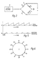
- Figure 2 is a circuit diagram showing the detector of Figure 1 connected in a bridge network;
- Figures 3 and 4 are graphs showing the output of the bridge for positive and negative bias applied to the detector of Figure 1 as a function of the position of a small spot of illumination;
- Figure 5 is a graph showing the bridge output when a spot of infra red radiation is scanned repetitively along the detector;
- Figures 6 and 7 are views of detectors having a plurality of electrodes so that azimuth and elevation positional information is obtainable;
- Figure 8 is a plan view of a detector showing contours of constant sensitivity for a field applied between opposing parallel electrodes.
- As seen in Figure 1 a detector system 1 comprises a piece of infra
red detector material 2 such as the ternary alloy CdxHg,_xTe. Typical dimensions are 100 pm2. Strip electrodes 3, 4 are attached along two opposite edges of thedetector material 2. Thedetector envelope 5 above an infra red transparent window 6 e.g. of germanium and cooled byliquid nitrogen 7. - A mirror 8 and
lenses detector material 2. The mirror 8 may be fixed, or oscillated as described later. - The detector of Figure 1 is connected in a
bridge network 11 as shown in Figure 2. Thisbridge 11 comprises two fixed resistors Ri, R2, and a variable resistor R3 for balancing. Input to thebridge 11, either D.C. or A.C. is from avoltage supply 12. - When a
spot area 13 of thedetector 2 is illuminated with infra red radiation photo carriers are generated. Let the detector length betweenelectrodes 3, 4, be 2a and the position of the illuminated spot measured from the centre be x, Figures 3, 4. For n-type material with a carrier concentration of about 5x 10'4 cm-3 applying a positive voltage toelectrode 3 causes a photo carrier drift to the right. When the applied field is sufficiently high e.g. 30 volts/cm the minority carriers are swept towards the earth contact 4, where they recombine. For steady state conditions the change of resistance betweenelectrodes 3, 4 is proportional to the distance photo carriers drift before recombining. The part of detector material carrying the drifting carriers is of reduced resistance compared to the remainder of the detector material. Figure 3 shows the resistance change betweenelectrodes 3, 4 for varying values of x, the position ofconstant spot 13 illumination. At the right hand edge carriers recombine into electrode 4 as they are formed, i.e. zero drift path length, and so the resistance change developed is zero. At the left hand edge the carriers drift the whole length of detector, i.e. drift path length is 2a, and the resistance change betweenelectrodes 3,4 is at a maximum value of AMAX. - Similarly when a negative potential is applied to
electrode 3 the carriers drift to the left Figure 4. The minimum resistance change, developed occurs when the illuminatingspot 13 is by theleft hand electrode 3, and the maximum resistance change BMAX occurs when thespot 13 is near the right hand electrode 4. - The position x, along the
detector 2 of illuminatingspot 13 as determined by measuring A, B, as follows:


- For example if the change in the negative direction, equals the change in the positive direction (B=A) then x=0, the centre.
- Thus by applying first a positive potential and then a negative potential to
electrode 3 the position of the illuminatingspot 13 is obtained. For example the position of 5 um diameter spot along a 50 um length is obtained. - The responses shown in Figures 3, 4 are idealised. In practice the curves are not quite linear in the centre region and may differ considerably near the
contacts 3, 4. Corrections for these variations may be allowed for using a look up table e.g. using a programmed read only memory (PROM). - The bridge of Figure 2 may be adjusted to give zero output for zero point illumination, or zero uniform illumination. When balanced for zero illumination, uniform illumination over the complete detector from background radiation will give A=B corresponding to an apparent x=0. When balanced for uniform background illumination A=B=0. Deviation of background will cause a spurious signal corresponding to an apparent target at x=0 because the equations for x above do not apply to uniform illumination. Thus continuous monitoring of background is desirable and the bridge balanced accordingly.
- The effect of background illumination and bias pedestal can be removed by scanning the
spot 13 along thedetector 2 with the mirror 8. Figures 5a shows a graph of mirror 8 position which is caused by scan in a saw-toothed manner. As the mirror scans it sweeps aspot 13 of infra red radiation along thedetector 2 in a direction opposite to photo carrier drift. This results in a ramp response on the bridge output as shown in Figure 5b. The position of this ramp signal within each scan represents the angular position of the target forming thespot 13 relative to the scan extreme positions. The length of the ramp signal is a function of detector length and system optics. Target angular position is thus determined by a timing circuit which times the intervalΦ between a synchronisation pulse at the beginning of each scan and receipt of the ramp signal (leading or trailing edge). - The above arrangement can be extended to determine the angular position of a plurality of infra red sources. Each source will be detected as a ramp voltage by the bridge.
- In an alternative arrangement the mirror 8 is caused to precess or wobble so that a
spot 13 moves in a small circle on thedetector 2. This gives a bridge output signal

- In both the scanning and wobbling system the mirror movement is slow in comparison with carrier drift velocity. For example carrier lifetime may be 1 to 10 us, drift velocity 5x10³ to 5x104 cm/s depending on
bias pedestal 2 to 20 mA, scan velocity 1/10xdrift velocity, modulation velocity 1/10 drift velocity. - Another form of the invention uses a high frequency bias applied by the
voltage supply 12. This is arranged such that: - frequency f2: VE/2a
- µ is typically 300 cm2Ns.
- E is peak field
- 2a is distance between
contacts 3, 4. - With such a high frequency bias carriers are not swept out within each half cycle but are swept alternately towards
contacts 3, 4 on alternate half cycles and reach thecontacts 3, 4 by diffusion. - For a
spot 13 in the centre of thedetector 2 carriers reach bothcontacts 3, 4 equally by diffusion. When thespot 13 is displaced away from the centre then carriers are preferentially lost at the nearest contact. This leads to an asymmetry in the output (A.C.) signal at theelectrodes 3, 4. The amount and direction of A.C. offset indicates spot position x on thedetector 2, and the A.C. value indicatesspot 13 intensity. - Alternatively the A.C. offset may be adjusted to zero by applying a D.C. bias feedback to the
voltage supply 12. This optimises sensitivity by maximising carrier life time over complete cycles. The spot position is related to the amount of D.C. bias applied. - The above systems provide only positional information x. To provide both azimuth and elevation position the detector may be provided with a plurality of opposed electrode pairs as shown in Figures 6, 7.
- In Figure 6 a
detector 2 is arranged as a disc with discrete pairs of opposingelectrodes 20, 20' to 25, 25'. Similarly a square shaped detector 2 (Figure 7) has discrete opposing electrodes 30,30' to 34, 34' and 35, 35' to 39, 39'. - Each opposing electrode e.g. 20, 20' is connected in sequence into a
bridge 11 whilst the remaining contacts remain disconnected, at a floating potential. Treating the information from each pair of contacts as previously described indicates both r, and θ information in Figure 6. To obtain x, information in Figure 7 bias is applied between electrodes 30-34 and 30'-34' and measurements proceed as in Figure 1, electrodes 35-39 and 35'-39' remain unconnected. - Similarly to obtain y information bias is applied between
electrodes 35―39 and electrodes 35'-39' whilst electrodes 30-34 and 30'-34' are unconnected. - Another method of determining x, y uses the arrangement of Figure 1. The effect of applying bias to
electrodes 3,4 is to produce in thedetector 2 variations in sensitivity as shown in Figure 8 which indicates contours of constant sensitivity. As shown these increase towardselectrodes 3 but reverse with reverse applied bias. The contours are symmetric about a lengthwise axis X X. - The mirror 8 is caused to wobble thus sweeping a
spot 13 of radiation in acircle 14. The effect of sweeping thespot 13 in a circle is to cause a periodic fluctuation in the detector response as measured at theelectrodes 3, 4. For a spot along the line XX the maximum response occurs when the spot isnearest electrode 3. This position may be taken as a zero phase position of the mirror 8. Forspot 13 incident on thedetector 2 above or below the line XX the maximum detector response occurs where thecircles 14 tangent is parallel to a contour line and nearest toelectrode 3. This maximum response occurs at some mirror phase angle ±Φ. The measurement of x and Φ uniquely indicates the position of a circle 14 (spot 13) on thedetector 2. Thus information on x and q) may be fed into a look-up table formed in a random access read only memory RAROM. The resultant output is thus the x, y position of aspot 13 on thedetector 2.
Claims (13)
Applications Claiming Priority (2)
| Application Number | Priority Date | Filing Date | Title |
|---|---|---|---|
| GB8211291 | 1982-04-19 | ||
| GB8211291 | 1982-04-19 |
Publications (3)
| Publication Number | Publication Date |
|---|---|
| EP0092330A2 EP0092330A2 (en) | 1983-10-26 |
| EP0092330A3 EP0092330A3 (en) | 1986-02-05 |
| EP0092330B1 true EP0092330B1 (en) | 1990-01-10 |
Family
ID=10529777
Family Applications (1)
| Application Number | Title | Priority Date | Filing Date |
|---|---|---|---|
| EP83301817A Expired - Lifetime EP0092330B1 (en) | 1982-04-19 | 1983-03-30 | Infra red photo detector systems |
Country Status (7)
| Country | Link |
|---|---|
| US (2) | US4572953A (en) |
| EP (1) | EP0092330B1 (en) |
| JP (1) | JPS58206933A (en) |
| CA (1) | CA1248199A (en) |
| DE (1) | DE3381093D1 (en) |
| GB (1) | GB2119508B (en) |
| IL (1) | IL68381A (en) |
Families Citing this family (4)
| Publication number | Priority date | Publication date | Assignee | Title |
|---|---|---|---|---|
| EP0452634B1 (en) * | 1990-03-16 | 1997-05-02 | Sumitomo Electric Industries, Ltd. | Lead frame for semiconductor device |
| US5354983A (en) * | 1990-04-10 | 1994-10-11 | Auto-Sense, Limited | Object detector utilizing a threshold detection distance and suppression means for detecting the presence of a motor vehicle |
| IL99592A (en) * | 1991-09-27 | 1995-05-26 | Bendix Avelex Inc | Thermal imaging apparatus |
| US5438199A (en) * | 1994-09-06 | 1995-08-01 | Alliedsignal Inc. | Thermal imaging apparatus with bias modulation |
Citations (4)
| Publication number | Priority date | Publication date | Assignee | Title |
|---|---|---|---|---|
| GB947883A (en) * | 1961-03-20 | 1964-01-29 | Giannini Controls Corp | Improvements in or relating to adjustable electrical potentiometers |
| US3400276A (en) * | 1965-12-29 | 1968-09-03 | Gen Precision Inc | Directional radiation sensor comprising a three-dimensional photosensitive surface |
| US3995159A (en) * | 1974-11-27 | 1976-11-30 | The Secretary Of State For Defense In Her Britannic Majesty's Government Of The United Kingdom Of Great Britain And Northern Ireland | Thermal imaging systems |
| US4004148A (en) * | 1976-02-02 | 1977-01-18 | General Electric Company | Accumulation mode charge injection infrared sensor |
Family Cites Families (8)
| Publication number | Priority date | Publication date | Assignee | Title |
|---|---|---|---|---|
| GB780089A (en) * | 1955-01-26 | 1957-07-31 | Marconi Wireless Telegraph Co | Improvements in or relating to measuring instruments and gauges |
| US3825795A (en) * | 1960-09-19 | 1974-07-23 | Gen Electric | Photoconductive camera tube and methods of manufacture |
| US3445667A (en) * | 1965-09-20 | 1969-05-20 | North American Rockwell | Photosensitive semiconductor device for obtaining light source position data |
| US3870887A (en) * | 1973-10-10 | 1975-03-11 | Mc Donnell Douglas Corp | Optical image position indicator means using time and phase delay sensing |
| US3963925A (en) * | 1975-02-26 | 1976-06-15 | Texas Instruments Incorporated | Photoconductive detector and method of fabrication |
| GB2095900B (en) * | 1981-03-30 | 1985-01-09 | Philips Electronic Associated | Imaging devices and systems |
| GB2095899B (en) * | 1981-03-30 | 1984-10-17 | Philips Electronic Associated | Imaging devices and systems |
| GB2099653B (en) * | 1981-06-03 | 1985-09-04 | Ferranti Ltd | Position sensing apparatus |
-
1983
- 1983-03-30 EP EP83301817A patent/EP0092330B1/en not_active Expired - Lifetime
- 1983-03-30 DE DE8383301817T patent/DE3381093D1/en not_active Expired - Lifetime
- 1983-04-08 CA CA000425529A patent/CA1248199A/en not_active Expired
- 1983-04-12 GB GB08309864A patent/GB2119508B/en not_active Expired
- 1983-04-14 IL IL68381A patent/IL68381A/en not_active IP Right Cessation
- 1983-04-18 US US06/485,888 patent/US4572953A/en not_active Expired - Lifetime
- 1983-04-18 JP JP58068240A patent/JPS58206933A/en active Pending
-
1985
- 1985-10-04 US US06/784,469 patent/US4691107A/en not_active Expired - Lifetime
Patent Citations (4)
| Publication number | Priority date | Publication date | Assignee | Title |
|---|---|---|---|---|
| GB947883A (en) * | 1961-03-20 | 1964-01-29 | Giannini Controls Corp | Improvements in or relating to adjustable electrical potentiometers |
| US3400276A (en) * | 1965-12-29 | 1968-09-03 | Gen Precision Inc | Directional radiation sensor comprising a three-dimensional photosensitive surface |
| US3995159A (en) * | 1974-11-27 | 1976-11-30 | The Secretary Of State For Defense In Her Britannic Majesty's Government Of The United Kingdom Of Great Britain And Northern Ireland | Thermal imaging systems |
| US4004148A (en) * | 1976-02-02 | 1977-01-18 | General Electric Company | Accumulation mode charge injection infrared sensor |
Also Published As
| Publication number | Publication date |
|---|---|
| US4691107A (en) | 1987-09-01 |
| GB2119508A (en) | 1983-11-16 |
| GB2119508B (en) | 1985-12-18 |
| EP0092330A2 (en) | 1983-10-26 |
| IL68381A0 (en) | 1983-07-31 |
| GB8309864D0 (en) | 1983-05-18 |
| US4572953A (en) | 1986-02-25 |
| DE3381093D1 (en) | 1990-02-15 |
| CA1248199A (en) | 1989-01-03 |
| EP0092330A3 (en) | 1986-02-05 |
| JPS58206933A (en) | 1983-12-02 |
| IL68381A (en) | 1988-07-31 |
Similar Documents
| Publication | Publication Date | Title |
|---|---|---|
| Kanadef et al. | A Very Fast VLSI Rangefinder1 | |
| Hashimoto et al. | People count system using multi-sensing application | |
| US3033073A (en) | Photoconductive locating device | |
| Spirig et al. | The multitap lock-in CCD with offset subtraction | |
| JP3349503B2 (en) | Method and apparatus for parameter difference imaging of sample surface | |
| Sarro et al. | An integrated thermal infrared sensing array | |
| US3453887A (en) | Temperature change measuring device | |
| US4585934A (en) | Self-calibration technique for charge-coupled device imagers | |
| JP2760146B2 (en) | Thermal image detector | |
| US4691107A (en) | Infra red photo detector systems | |
| US3415992A (en) | Extended area semiconductor radiation detectors and a novel readout arrangement | |
| US3237010A (en) | Navigational system using infra-red horizon sensors | |
| JPS58108425A (en) | Method of applying bias to photoconduction detector, detecting device and detector formed for said device | |
| US4979816A (en) | Range sensing system | |
| JP3101190B2 (en) | Infrared detector | |
| US3912398A (en) | Stroboscopic celestial scanner | |
| US3846028A (en) | Energy conversion apparatus | |
| Phelan et al. | Imaging and storage with a uniform MOS structure | |
| US5142150A (en) | Horizon sensor for satellites using superconductor(s) having a high critical temperature | |
| Ferrari et al. | Displacement sensor based on pyroelectric thick films and contactless light-spot cursor | |
| Middelhoek et al. | Silicon and Hybrid Micro‐Electronic Sensors | |
| US3495085A (en) | Apparatus for tracking an infrared radiation gradient and readout means therefor | |
| US4633092A (en) | Light sensing device | |
| US3418481A (en) | Illumination detector using a plurality of light sensitive diode pairs | |
| Martins et al. | Detection Limits of a nip a-Si: H Linear Array Position Sensitive Detector |
Legal Events
| Date | Code | Title | Description |
|---|---|---|---|
| PUAI | Public reference made under article 153(3) epc to a published international application that has entered the european phase |
Free format text: ORIGINAL CODE: 0009012 |
|
| AK | Designated contracting states |
Designated state(s): DE FR GB NL |
|
| PUAL | Search report despatched |
Free format text: ORIGINAL CODE: 0009013 |
|
| AK | Designated contracting states |
Designated state(s): DE FR GB NL |
|
| 17P | Request for examination filed |
Effective date: 19860801 |
|
| 17Q | First examination report despatched |
Effective date: 19871123 |
|
| GRAA | (expected) grant |
Free format text: ORIGINAL CODE: 0009210 |
|
| AK | Designated contracting states |
Kind code of ref document: B1 Designated state(s): DE FR GB NL |
|
| ET | Fr: translation filed | ||
| REF | Corresponds to: |
Ref document number: 3381093 Country of ref document: DE Date of ref document: 19900215 |
|
| PLBE | No opposition filed within time limit |
Free format text: ORIGINAL CODE: 0009261 |
|
| STAA | Information on the status of an ep patent application or granted ep patent |
Free format text: STATUS: NO OPPOSITION FILED WITHIN TIME LIMIT |
|
| 26N | No opposition filed | ||
| PGFP | Annual fee paid to national office [announced via postgrant information from national office to epo] |
Ref country code: FR Payment date: 19990208 Year of fee payment: 17 |
|
| PGFP | Annual fee paid to national office [announced via postgrant information from national office to epo] |
Ref country code: GB Payment date: 19990216 Year of fee payment: 17 |
|
| PGFP | Annual fee paid to national office [announced via postgrant information from national office to epo] |
Ref country code: NL Payment date: 19990224 Year of fee payment: 17 |
|
| PGFP | Annual fee paid to national office [announced via postgrant information from national office to epo] |
Ref country code: DE Payment date: 19990226 Year of fee payment: 17 |
|
| PG25 | Lapsed in a contracting state [announced via postgrant information from national office to epo] |
Ref country code: GB Free format text: LAPSE BECAUSE OF NON-PAYMENT OF DUE FEES Effective date: 20000330 |
|
| PG25 | Lapsed in a contracting state [announced via postgrant information from national office to epo] |
Ref country code: NL Free format text: LAPSE BECAUSE OF NON-PAYMENT OF DUE FEES Effective date: 20001001 |
|
| GBPC | Gb: european patent ceased through non-payment of renewal fee |
Effective date: 20000330 |
|
| PG25 | Lapsed in a contracting state [announced via postgrant information from national office to epo] |
Ref country code: FR Free format text: LAPSE BECAUSE OF NON-PAYMENT OF DUE FEES Effective date: 20001130 |
|
| NLV4 | Nl: lapsed or anulled due to non-payment of the annual fee |
Effective date: 20001001 |
|
| REG | Reference to a national code |
Ref country code: FR Ref legal event code: ST |
|
| PG25 | Lapsed in a contracting state [announced via postgrant information from national office to epo] |
Ref country code: DE Free format text: LAPSE BECAUSE OF NON-PAYMENT OF DUE FEES Effective date: 20010103 |