EP0091686A2 - Semiconductor device having a diffused region of reduced length and method of fabricating the same - Google Patents
Semiconductor device having a diffused region of reduced length and method of fabricating the same Download PDFInfo
- Publication number
- EP0091686A2 EP0091686A2 EP83103501A EP83103501A EP0091686A2 EP 0091686 A2 EP0091686 A2 EP 0091686A2 EP 83103501 A EP83103501 A EP 83103501A EP 83103501 A EP83103501 A EP 83103501A EP 0091686 A2 EP0091686 A2 EP 0091686A2
- Authority
- EP
- European Patent Office
- Prior art keywords
- region
- invention according
- mosfet
- source
- type
- Prior art date
- Legal status (The legal status is an assumption and is not a legal conclusion. Google has not performed a legal analysis and makes no representation as to the accuracy of the status listed.)
- Granted
Links
- 239000004065 semiconductor Substances 0.000 title claims abstract description 37
- 238000004519 manufacturing process Methods 0.000 title claims abstract description 15
- 238000009792 diffusion process Methods 0.000 claims abstract description 21
- 239000002019 doping agent Substances 0.000 claims description 16
- 239000000758 substrate Substances 0.000 claims description 13
- 239000011819 refractory material Substances 0.000 claims description 12
- 229910052710 silicon Inorganic materials 0.000 claims description 11
- 239000010703 silicon Substances 0.000 claims description 11
- 230000001419 dependent effect Effects 0.000 claims description 7
- 238000005530 etching Methods 0.000 claims description 7
- 230000004888 barrier function Effects 0.000 claims description 6
- 239000013078 crystal Substances 0.000 claims description 4
- 230000000149 penetrating effect Effects 0.000 claims 1
- 230000003071 parasitic effect Effects 0.000 abstract description 16
- 238000000034 method Methods 0.000 abstract description 13
- 238000001465 metallisation Methods 0.000 description 10
- XUIMIQQOPSSXEZ-UHFFFAOYSA-N Silicon Chemical compound [Si] XUIMIQQOPSSXEZ-UHFFFAOYSA-N 0.000 description 9
- 229910021420 polycrystalline silicon Inorganic materials 0.000 description 7
- 229920005591 polysilicon Polymers 0.000 description 7
- KWYUFKZDYYNOTN-UHFFFAOYSA-M Potassium hydroxide Chemical compound [OH-].[K+] KWYUFKZDYYNOTN-UHFFFAOYSA-M 0.000 description 6
- VYPSYNLAJGMNEJ-UHFFFAOYSA-N Silicium dioxide Chemical compound O=[Si]=O VYPSYNLAJGMNEJ-UHFFFAOYSA-N 0.000 description 6
- 230000004048 modification Effects 0.000 description 6
- 238000012986 modification Methods 0.000 description 6
- 239000000463 material Substances 0.000 description 5
- 238000010276 construction Methods 0.000 description 3
- 150000002500 ions Chemical class 0.000 description 3
- 238000000206 photolithography Methods 0.000 description 3
- 239000000377 silicon dioxide Substances 0.000 description 3
- 235000012239 silicon dioxide Nutrition 0.000 description 3
- 238000006467 substitution reaction Methods 0.000 description 3
- KFZMGEQAYNKOFK-UHFFFAOYSA-N Isopropanol Chemical compound CC(C)O KFZMGEQAYNKOFK-UHFFFAOYSA-N 0.000 description 2
- 238000010420 art technique Methods 0.000 description 2
- QVGXLLKOCUKJST-UHFFFAOYSA-N atomic oxygen Chemical compound [O] QVGXLLKOCUKJST-UHFFFAOYSA-N 0.000 description 2
- 230000000903 blocking effect Effects 0.000 description 2
- TWNQGVIAIRXVLR-UHFFFAOYSA-N oxo(oxoalumanyloxy)alumane Chemical compound O=[Al]O[Al]=O TWNQGVIAIRXVLR-UHFFFAOYSA-N 0.000 description 2
- 229910052760 oxygen Inorganic materials 0.000 description 2
- 239000001301 oxygen Substances 0.000 description 2
- 238000005549 size reduction Methods 0.000 description 2
- ZOXJGFHDIHLPTG-UHFFFAOYSA-N Boron Chemical compound [B] ZOXJGFHDIHLPTG-UHFFFAOYSA-N 0.000 description 1
- OAICVXFJPJFONN-UHFFFAOYSA-N Phosphorus Chemical compound [P] OAICVXFJPJFONN-UHFFFAOYSA-N 0.000 description 1
- 230000002411 adverse Effects 0.000 description 1
- YXTPWUNVHCYOSP-UHFFFAOYSA-N bis($l^{2}-silanylidene)molybdenum Chemical compound [Si]=[Mo]=[Si] YXTPWUNVHCYOSP-UHFFFAOYSA-N 0.000 description 1
- 229910052796 boron Inorganic materials 0.000 description 1
- 230000000295 complement effect Effects 0.000 description 1
- 238000007796 conventional method Methods 0.000 description 1
- 230000006378 damage Effects 0.000 description 1
- 230000000694 effects Effects 0.000 description 1
- 230000005669 field effect Effects 0.000 description 1
- 239000011810 insulating material Substances 0.000 description 1
- 230000007246 mechanism Effects 0.000 description 1
- 239000000203 mixture Substances 0.000 description 1
- 229910021344 molybdenum silicide Inorganic materials 0.000 description 1
- 230000001590 oxidative effect Effects 0.000 description 1
- 229910052698 phosphorus Inorganic materials 0.000 description 1
- 239000011574 phosphorus Substances 0.000 description 1
- 238000001020 plasma etching Methods 0.000 description 1
- 230000000063 preceeding effect Effects 0.000 description 1
- 230000008569 process Effects 0.000 description 1
- WQJQOUPTWCFRMM-UHFFFAOYSA-N tungsten disilicide Chemical compound [Si]#[W]#[Si] WQJQOUPTWCFRMM-UHFFFAOYSA-N 0.000 description 1
- 229910021342 tungsten silicide Inorganic materials 0.000 description 1
Images


Classifications
-
- H—ELECTRICITY
- H01—ELECTRIC ELEMENTS
- H01L—SEMICONDUCTOR DEVICES NOT COVERED BY CLASS H10
- H01L29/00—Semiconductor devices adapted for rectifying, amplifying, oscillating or switching, or capacitors or resistors with at least one potential-jump barrier or surface barrier, e.g. PN junction depletion layer or carrier concentration layer; Details of semiconductor bodies or of electrodes thereof ; Multistep manufacturing processes therefor
- H01L29/66—Types of semiconductor device ; Multistep manufacturing processes therefor
- H01L29/68—Types of semiconductor device ; Multistep manufacturing processes therefor controllable by only the electric current supplied, or only the electric potential applied, to an electrode which does not carry the current to be rectified, amplified or switched
- H01L29/76—Unipolar devices, e.g. field effect transistors
- H01L29/772—Field effect transistors
- H01L29/78—Field effect transistors with field effect produced by an insulated gate
- H01L29/7801—DMOS transistors, i.e. MISFETs with a channel accommodating body or base region adjoining a drain drift region
- H01L29/7802—Vertical DMOS transistors, i.e. VDMOS transistors
-
- H—ELECTRICITY
- H01—ELECTRIC ELEMENTS
- H01L—SEMICONDUCTOR DEVICES NOT COVERED BY CLASS H10
- H01L21/00—Processes or apparatus adapted for the manufacture or treatment of semiconductor or solid state devices or of parts thereof
- H01L21/02—Manufacture or treatment of semiconductor devices or of parts thereof
- H01L21/04—Manufacture or treatment of semiconductor devices or of parts thereof the devices having at least one potential-jump barrier or surface barrier, e.g. PN junction, depletion layer or carrier concentration layer
- H01L21/18—Manufacture or treatment of semiconductor devices or of parts thereof the devices having at least one potential-jump barrier or surface barrier, e.g. PN junction, depletion layer or carrier concentration layer the devices having semiconductor bodies comprising elements of Group IV of the Periodic System or AIIIBV compounds with or without impurities, e.g. doping materials
- H01L21/30—Treatment of semiconductor bodies using processes or apparatus not provided for in groups H01L21/20 - H01L21/26
- H01L21/302—Treatment of semiconductor bodies using processes or apparatus not provided for in groups H01L21/20 - H01L21/26 to change their surface-physical characteristics or shape, e.g. etching, polishing, cutting
- H01L21/306—Chemical or electrical treatment, e.g. electrolytic etching
- H01L21/30604—Chemical etching
- H01L21/30608—Anisotropic liquid etching
-
- H—ELECTRICITY
- H01—ELECTRIC ELEMENTS
- H01L—SEMICONDUCTOR DEVICES NOT COVERED BY CLASS H10
- H01L21/00—Processes or apparatus adapted for the manufacture or treatment of semiconductor or solid state devices or of parts thereof
- H01L21/02—Manufacture or treatment of semiconductor devices or of parts thereof
- H01L21/04—Manufacture or treatment of semiconductor devices or of parts thereof the devices having at least one potential-jump barrier or surface barrier, e.g. PN junction, depletion layer or carrier concentration layer
- H01L21/18—Manufacture or treatment of semiconductor devices or of parts thereof the devices having at least one potential-jump barrier or surface barrier, e.g. PN junction, depletion layer or carrier concentration layer the devices having semiconductor bodies comprising elements of Group IV of the Periodic System or AIIIBV compounds with or without impurities, e.g. doping materials
- H01L21/30—Treatment of semiconductor bodies using processes or apparatus not provided for in groups H01L21/20 - H01L21/26
- H01L21/302—Treatment of semiconductor bodies using processes or apparatus not provided for in groups H01L21/20 - H01L21/26 to change their surface-physical characteristics or shape, e.g. etching, polishing, cutting
- H01L21/306—Chemical or electrical treatment, e.g. electrolytic etching
- H01L21/308—Chemical or electrical treatment, e.g. electrolytic etching using masks
-
- H—ELECTRICITY
- H01—ELECTRIC ELEMENTS
- H01L—SEMICONDUCTOR DEVICES NOT COVERED BY CLASS H10
- H01L29/00—Semiconductor devices adapted for rectifying, amplifying, oscillating or switching, or capacitors or resistors with at least one potential-jump barrier or surface barrier, e.g. PN junction depletion layer or carrier concentration layer; Details of semiconductor bodies or of electrodes thereof ; Multistep manufacturing processes therefor
- H01L29/02—Semiconductor bodies ; Multistep manufacturing processes therefor
- H01L29/06—Semiconductor bodies ; Multistep manufacturing processes therefor characterised by their shape; characterised by the shapes, relative sizes, or dispositions of the semiconductor regions ; characterised by the concentration or distribution of impurities within semiconductor regions
- H01L29/10—Semiconductor bodies ; Multistep manufacturing processes therefor characterised by their shape; characterised by the shapes, relative sizes, or dispositions of the semiconductor regions ; characterised by the concentration or distribution of impurities within semiconductor regions with semiconductor regions connected to an electrode not carrying current to be rectified, amplified or switched and such electrode being part of a semiconductor device which comprises three or more electrodes
- H01L29/1095—Body region, i.e. base region, of DMOS transistors or IGBTs
-
- H—ELECTRICITY
- H01—ELECTRIC ELEMENTS
- H01L—SEMICONDUCTOR DEVICES NOT COVERED BY CLASS H10
- H01L29/00—Semiconductor devices adapted for rectifying, amplifying, oscillating or switching, or capacitors or resistors with at least one potential-jump barrier or surface barrier, e.g. PN junction depletion layer or carrier concentration layer; Details of semiconductor bodies or of electrodes thereof ; Multistep manufacturing processes therefor
- H01L29/66—Types of semiconductor device ; Multistep manufacturing processes therefor
- H01L29/66007—Multistep manufacturing processes
- H01L29/66075—Multistep manufacturing processes of devices having semiconductor bodies comprising group 14 or group 13/15 materials
- H01L29/66227—Multistep manufacturing processes of devices having semiconductor bodies comprising group 14 or group 13/15 materials the devices being controllable only by the electric current supplied or the electric potential applied, to an electrode which does not carry the current to be rectified, amplified or switched, e.g. three-terminal devices
- H01L29/66234—Bipolar junction transistors [BJT]
- H01L29/66325—Bipolar junction transistors [BJT] controlled by field-effect, e.g. insulated gate bipolar transistors [IGBT]
- H01L29/66333—Vertical insulated gate bipolar transistors
- H01L29/66348—Vertical insulated gate bipolar transistors with a recessed gate
-
- H—ELECTRICITY
- H01—ELECTRIC ELEMENTS
- H01L—SEMICONDUCTOR DEVICES NOT COVERED BY CLASS H10
- H01L29/00—Semiconductor devices adapted for rectifying, amplifying, oscillating or switching, or capacitors or resistors with at least one potential-jump barrier or surface barrier, e.g. PN junction depletion layer or carrier concentration layer; Details of semiconductor bodies or of electrodes thereof ; Multistep manufacturing processes therefor
- H01L29/66—Types of semiconductor device ; Multistep manufacturing processes therefor
- H01L29/68—Types of semiconductor device ; Multistep manufacturing processes therefor controllable by only the electric current supplied, or only the electric potential applied, to an electrode which does not carry the current to be rectified, amplified or switched
- H01L29/70—Bipolar devices
- H01L29/72—Transistor-type devices, i.e. able to continuously respond to applied control signals
- H01L29/739—Transistor-type devices, i.e. able to continuously respond to applied control signals controlled by field-effect, e.g. bipolar static induction transistors [BSIT]
- H01L29/7393—Insulated gate bipolar mode transistors, i.e. IGBT; IGT; COMFET
- H01L29/7395—Vertical transistors, e.g. vertical IGBT
- H01L29/7396—Vertical transistors, e.g. vertical IGBT with a non planar surface, e.g. with a non planar gate or with a trench or recess or pillar in the surface of the emitter, base or collector region for improving current density or short circuiting the emitter and base regions
- H01L29/7397—Vertical transistors, e.g. vertical IGBT with a non planar surface, e.g. with a non planar gate or with a trench or recess or pillar in the surface of the emitter, base or collector region for improving current density or short circuiting the emitter and base regions and a gate structure lying on a slanted or vertical surface or formed in a groove, e.g. trench gate IGBT
-
- H—ELECTRICITY
- H01—ELECTRIC ELEMENTS
- H01L—SEMICONDUCTOR DEVICES NOT COVERED BY CLASS H10
- H01L29/00—Semiconductor devices adapted for rectifying, amplifying, oscillating or switching, or capacitors or resistors with at least one potential-jump barrier or surface barrier, e.g. PN junction depletion layer or carrier concentration layer; Details of semiconductor bodies or of electrodes thereof ; Multistep manufacturing processes therefor
- H01L29/66—Types of semiconductor device ; Multistep manufacturing processes therefor
- H01L29/68—Types of semiconductor device ; Multistep manufacturing processes therefor controllable by only the electric current supplied, or only the electric potential applied, to an electrode which does not carry the current to be rectified, amplified or switched
- H01L29/76—Unipolar devices, e.g. field effect transistors
- H01L29/772—Field effect transistors
- H01L29/78—Field effect transistors with field effect produced by an insulated gate
- H01L29/7801—DMOS transistors, i.e. MISFETs with a channel accommodating body or base region adjoining a drain drift region
- H01L29/7802—Vertical DMOS transistors, i.e. VDMOS transistors
- H01L29/7813—Vertical DMOS transistors, i.e. VDMOS transistors with trench gate electrode, e.g. UMOS transistors
-
- H—ELECTRICITY
- H01—ELECTRIC ELEMENTS
- H01L—SEMICONDUCTOR DEVICES NOT COVERED BY CLASS H10
- H01L29/00—Semiconductor devices adapted for rectifying, amplifying, oscillating or switching, or capacitors or resistors with at least one potential-jump barrier or surface barrier, e.g. PN junction depletion layer or carrier concentration layer; Details of semiconductor bodies or of electrodes thereof ; Multistep manufacturing processes therefor
- H01L29/40—Electrodes ; Multistep manufacturing processes therefor
- H01L29/41—Electrodes ; Multistep manufacturing processes therefor characterised by their shape, relative sizes or dispositions
- H01L29/417—Electrodes ; Multistep manufacturing processes therefor characterised by their shape, relative sizes or dispositions carrying the current to be rectified, amplified or switched
- H01L29/41725—Source or drain electrodes for field effect devices
- H01L29/41766—Source or drain electrodes for field effect devices with at least part of the source or drain electrode having contact below the semiconductor surface, e.g. the source or drain electrode formed at least partially in a groove or with inclusions of conductor inside the semiconductor
-
- H—ELECTRICITY
- H01—ELECTRIC ELEMENTS
- H01L—SEMICONDUCTOR DEVICES NOT COVERED BY CLASS H10
- H01L29/00—Semiconductor devices adapted for rectifying, amplifying, oscillating or switching, or capacitors or resistors with at least one potential-jump barrier or surface barrier, e.g. PN junction depletion layer or carrier concentration layer; Details of semiconductor bodies or of electrodes thereof ; Multistep manufacturing processes therefor
- H01L29/40—Electrodes ; Multistep manufacturing processes therefor
- H01L29/43—Electrodes ; Multistep manufacturing processes therefor characterised by the materials of which they are formed
- H01L29/49—Metal-insulator-semiconductor electrodes, e.g. gates of MOSFET
- H01L29/4966—Metal-insulator-semiconductor electrodes, e.g. gates of MOSFET the conductor material next to the insulator being a composite material, e.g. organic material, TiN, MoSi2
- H01L29/4975—Metal-insulator-semiconductor electrodes, e.g. gates of MOSFET the conductor material next to the insulator being a composite material, e.g. organic material, TiN, MoSi2 being a silicide layer, e.g. TiSi2
Definitions
- 0ur invention relates to a semiconductor device having a diffused region of reduced length forming the SOURCE or corresponding region in a device other than a MOSFET, and to a method of fabricating the same.
- Our invention is particularly useful in helping to prevent turn-on, or incipience of current conduction, in a parasitic bipolar transistor inherent in some types of semiconductor devices, such as MOSFETs or IGRs. Turn-on of such parasitic transistor is inevitably accompanied by a partial or total loss of control of current in the semiconductor device, and may even result in complete destruction of the device.
- a typical prior art device for instance, a MOSFET, incorporates a "electrical short", or low resistance connection, between the adjoining SOURCE and BASE regions, which have a P-N junction between them.
- the purpose is to prevent such P-N junction from becoming forward biased above a threshold level that would induce turn-on of the parasitic transistor.
- the distance between the short and the furthest part of the P-N junction which corresponds generally to the length of the SOURCE, should be minimized.
- the SOURCE however, has a minimum length typically in excess of about 10 micrometers, as a result of the prior art method of fabricating the MOSFET.
- a prior art MOSFET is made by diffusing into its BASE a suitable type dopant, through a diffusion window, to form its SOURCE. Thereafter, an etchant is applied to the an intermediate portion of SOURCE through an etch window, to etch through/the SOURCE. This requires aligning the etch window over the SOURCE, this alignment being a delicate procedure because the SOURCE is so small. Consequently, the SOURCE must be long enough to accommodate an alignment tolerance. It would thus be desirable to provide a semiconductor device having a diffused region (i.e., the SOURCE in a MOSFET) of reduced length.
- a further object of our invention is to provide a method of fabricating a semiconductor device not requiring a delicate alignment step for forming the SOURCE or corresponding. region in a device other than a MOSFET.
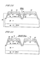
- FIGURE 1A is a schematic view in cross-section of a prior art MOSFET:
- FIGURE 1A illustrates a prior art MOSFET 10 having many identical "cells", or repeated units of structure. For simplicity, explicit reference is made only to the centrally depicted cell of the MOSFET 10.
- the MOSFET 10 is typically used to control the current level in an external circuit (not shown), which is connected between its SOURCE and drain electrodes 12 and 14.
- the "gate" or control electrode 16 normally determines such current level, depending upon the amplitude of a control voltage impressed on it.
- Normal operation of the MOSFET 10 is subject, however, to the adverse effect of turn-on of its inherent parasitic N-P-N transistor, formed from N region 18, P BASE 20, and N + SOURCE 22. If the parasitic transistor turns-on, the MOSFET 10 begins to lose control of the external circuit current level. The parasitic transistor can become so conductive that all control of the external circuit current level is lost, and the MOSFET 10 itself can be destroyed.
- the parasitic transistor will turn-on if any portion of the P-N junction 24 between P BASE 20 and N + SOURCE 22 (e.g., between locations A and C) becomes forward biased by more than about 0.7 volts (for a silicon device).
- an electrical short between P BASE 20 and N SOURCE 22 is implemented at location B by source electrode 12.
- the voltage drop across the P-N junction 24 at location B is held to 0 volts.
- This condition does not hold for portions of the P-N junction 24 remote from location B.
- the voltage drop between locations A and C can rise above 0.7 volts if sufficient hole current flows between locations A and B in P BASE 20, resulting in a voltage drop from location A to B.
- FIGURE 1B shows a semiconductor body 28 including N + DRAIN 30, N region 18, and P BASE 20.
- a diffusion barrier or mask 32 such as silicon diaxide,is provided on the upper surface 33 of the body 28.
- the diffusion mask 32 defines diffusion window 34 (and adjacent diffusion windows).
- An N diffusion of dopant through the upper surface 33 is performed and forms the N SOURCE 22 (shown in phantom).
- an etch barrier or mask 38 such as silicon dioxide, is next provided on the upper surface 33.
- the etch mask 38 defines an etch window 40.
- An etchant is applied through the etch window 40 to remove semiconductor material from the body 28 to form groove 42 (shown in phantom), necessary for implementing the completed MOSFET 10 (FIG.1).
- Proper construction of the N SOURCE 22 requires that the etch window 40 be aligned as closely as is feasible to the center of the N SOURCE 22. However, this alignment step is extremely delicate, since the dimensions involved are exceedingly minute (e.g., on the order of 5 microns).
- the foregoing alignment step is delicate, precise alignment is not consistently attainable. Consequently, the etch window 40 falls at random within a minimum alignment tolerance 44.
- the completed N SOURCE 22 must be lengthy. This, however, increases the risk of the parasitic transistor turning on.
- a further drawback of having the N + SOURCE 22 lengthy is that the individual size of each cell in the MOSFET 10 is increased. This undesirably limits the amount of current that the MOSFET 10 can carry, and reduces the manufacturing yield of operable MOSFETs. Additionally, the inclusion of the foregoing delicate alignment step further reduces the manufacturing yield of operable MOSFETs.
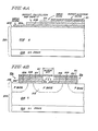
- FIGURES 2A-2G inclusive illustrating a preferred method of fabricating a MOSFET.
- N DRAIN 52 typically comprises a substrate layer, with N-type layer 54 epitaxially grown on N + DRAIN 52, and P BASE 56 . epitaxially grown (or diffused into) the N-type layer 54.
- This construction is typical of "power" MOSFET, or MOSFETs designed to carry substantial levels of current. Our invention, however, can be practised with non-power devices.
- FIGURE 2A additionally illustrates a processing step for implementing P region 58 (shown in phantom).
- P region 58 shown in phantom
- P-type dopant such as boron
- a thick layer e.g.,2 micrometers of silicon dioxide,or other suitable diffusion resistant material, to the body upper surface 60, and pattern it using photolithography (a known technique) to provide a mask 62, as shown in FIGURE 2B, which defines a window 64.
- This etching need not be anisotropic, or directional.
- a suitable etching technique for example, is planar plasma etching.
- N-type dopant such as phosphorus
- the mask 62 serves an additional purpose as an etch barrier or mask, as shown in FIGURE 2D.
- the etchant is dependent upon the crystal orientation of the silicon body 50 , such orientation being (100).
- Such etchant does not undercut beneath the mask 62 and hence/completely etch away the N + SOURCE 66. This allows portions of N + SOURCE 66 beneath the mask 62, or "shoulders" 72, to remain intact.
- an insulating layer 73 to cover the surface of the groove 68.
- a preferred way of implementing the layer 73 is by growing it as an oxide of the semiconductor body 50. This is accomplished by exposing the body 50 to oxygen at high temperature.
- the P region 58 advantageously completes an electrical short between P BASE 56 and N + SOURCE 66,e.g., location E.
- This electrical short has three components.
- One component comprises the junction 82 between the P region 58 and the N SOURCE 66,which junction forms a "tunnel" junction, because each of the foregoing regions is heavily doped(i.e.,each has a doping concentration in excess of about 10 19 dopant atoms per cc of silicon).
- the tunnel junction 82 constitutes a low resistance connection between the N + SOURCE 66 and the P + region 58,at least during normal device operation.
- Tunnel junctions are discussed more fully,for example, in S.M.Sze,Physics of Semiconductor Devices, New York: Wiley-Interscience,1969,Chapter 4.
- the second component of the electrical short /loca ti on E comprises the junction 84,between P BASE 56 and P + region 58.
- the junction 84 constitutes a low resistance path between the P BASE 56 and the P + region 58, because holes can freely pass from the P BASE.56 to the P + region 58.
- the third component of the electrical short/location E comprises the P region 58, in the vicinity/location E, between the tunnel junction 82 and the junction 84.
- the region 58 is highly doped, and so constitutes a low resistance path between the junctions 82 and 84. All three of the foregoing low resistance paths collectively provide a low resistance path between the P BASE 56 and the N SOURCE 66, thus implementing the electrical short between these regions at location E.
- the tunnel junction 82 is also part of a low resistance path between the N SOURCE 66 and the source electrode 76, such low resistance path also including the highly-doped P region 58. Because the P region 58 is highly-doped and thus conductive, the source electrode 76 only needs to make contact with it at isolated locations.
- the MOSFET 80 possesses significant advantages over the prior art MOSFET 10, described above.
- the length of the N + SOURCE 66 is drastically reduced compared to the prior art. This is because all but the shoulders 72 of the N SOURCE 66 have been etched away. Accordingly, the electrical short at location E is highly effective. This is because hole current flowing in P BASE 56, from location D to location E, produces only a low voltage drop because the distance D-E is short. Accordingly, it is unlikely that any portion of.P-N junction 86 between P BASE 56 and N + SOURCE 66 (e.g., between locations D and F) can become excessively forward biased. This greatly reduces the likelihood of turn-on of the parasitic bipolar transistor in the MOSFET 80(i.e., the transistor formed by N-region 54, P BASE 56, and N SOURCE 66).
- MOSFETs made by our invention allow reduced cell size using present state of the art processing techniques. For a typical MOSFET, this size reduction amounts to about 50 percent. This dramatically increases the manufacuring yield of operable MOSFETs, which makes them less increases the costly. Additionally, the size reduction/current-carrying capability of a 500 volt-rated MOSFET by about 30 percent, and of a 50 volt-rated MOSFET by about 100 percent. Accordingly, smaller and less costly MOSFETs made in accordance with our invention are needed in a given application, compared with MOSFETs made by the conventional methods.
- our foregoing method of fabricating the MOSFET 80 could be modified, for example, by employing an anisotropic etchant other than the preferred orientation-dependent etchant such mentioned above.
- suitable etchants must allow shoulders 72 of the N + SOURCE 66 to remain intact.
- these other suitable etchants include a vertically collimated beam of reactive ions and a planar plasma etchant. These etchants tend to form a groove 68 (FIGURE 2D) having more of a U-shape than a V-shape. These etchants do not to be require the semiconductor body/(100) crystal oriented, as does the preferred, orientation-dependent etchant.
- a further modification of our foregoing method of fabricating the MOSFET 80 is to form the gate electrode 74 from a conductive refractory material, rather than by metallization.
- Suitable refractory materials include highly-doped polysilicon, molybdenum silicide and tungsten silicide. If polysilicon were used, our foregoing method could be altered as follows, by way of example. After the insulating layer 62 of FIGURE 2E has been formed, polysilicon (not illustrated) is deposited on the upper surface of the structure shown in FIGURE 2E. The polysilicon layer is highly doped to make it conductive, and is patterned to remove it from the desired locations for the source electrode. A layer of oxide is grown on the polysilicon by exposing it to oxygen at high temperature, openings similar to openings 75 (FIGURE 2F) are made, and, finally, metallization is applied to the upper surface of the modified structure to implement the source electrode.
- IGR insulated gate rectifier
- FIGURE 3 Another appropriate semiconductor device is an insulated gate rectifier (IGR), shown in FIGURE 3.
- the IGR 90 includes a.P + substrate 92, in contrast with the N + DRAIN substrate 52 of the MOSFET 80. With this substitution, the foregoing method of fabricating the present embodiment of our invention is applicable to IGR 90.
- the parasitic N-P-N transistor in the IGR 90 formed by N region 94, P region 96, and N region 97, is electrically coupled in thyristor fashion to a parasitic P-N-P transistor -- namely, the transistor formed by P region 92, N region 94, and P region 96. Accordingly, these parasitic transistors can "latch", or become established in a current-conducting state, if the N-P-N (or upper transistor) is allowed to turn on. Once the IGR 90 becomes latched, control of its current level by its gate 98 is totally lost.
- This risk of the IGR 90 becoming latched is always present when the IGR 90 is in its active or current- carrying state.
- Our invention greatly diminishes this risk by preventing the N-P-N transistor from becoming excessively active. This is because the distance H-I in P region 96 along P-N junction 100 is so short that P-N junction 100 (e.g., between locations H and J)cannot become excessively forward biased. Additionally, the IGR 90 can have a reduced cell size, compared to IGRs made from prior art methods, enabling the IGR 90 to be made more economically and carry more current.
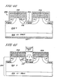
- FIGURE 4A a semiconductor body 200,typically of silicon.
- the body 200 typically comprises a substrate 202, constituting an N DRAIN,and an N region 204, typically epitaxially grown on the N + DRAIN 202.
- This construction is typical of power MOSFETs, although our invention can be practised with non-power devices.
- an insulating layer 206 On the upper surface 205 of the body 200, we form an insulating layer 206, suitably by growing an oxide on the body 200.
- a conductive refractory material 208 (shown partially broken away) on the insulating layer 206.
- the refractory material comprises polysilicon we dope it highly to make it conductive.
- insulating layer 210 on the upper surface of the refractory material 208.
- the insulating layer 210 suitably comprises an oxide grown thereon.
- the layer 211 comprises a material, such as aluminum oxide, which is resistant to an etchant,that etches through silicon dioxide and silicon during a processing step described below.
- the mask 216 defines a window 217 and serves as a diffusion barrier when we next make a P-type diffusion through the window 217 to form P BASE 218 (shown in phantom).
- N + SOURCE 220 (shown in phantom).
- the N diffusion extends laterally beneath the refractory material 208, i.e., in region 222, approximately the same distance as it diffuses vertically downward. This diffusion occurs at high temperature in an oxidizing atmosphere.
- the exposed surfaces 219(shown in FIGURE 4B) of the refractory material 208 become oxidized so that the refractory material 208 becomes surrounded by insulating material, as shown in FIGURE 4C.
- the exposed portions of the semiconductor body surface 205(shown in FIGURE 4B) becomes oxidized to form oxide layer 221,(shown in FIGURE 4C).
- this etchant suitably comprises a vertically collimated beam of reactive ions or a planar plasma etchant, and forms a generally U-shaped groove 224.
- a V-shaped groove (not illustrated) could be formed by first using one of the preceeding etchants to remove the oxide layer 221, and then using an orientation-dependent etchant (such as a mixture of potassium hydroxide and isopropanol, in the approximate ratio of 3 to 1) to etch into the semiconductor body 200.
- an orientation-dependent etchant such as a mixture of potassium hydroxide and isopropanol, in the approximate ratio of 3 to 1
- the body 200 would need to have a (100) crystal orientation, and an insulating layer 210 (FIGURE 4A) is necessary, because the layer 211 (at least where it comprises aluminum oxide) is removed by the orientation-dependent etchant (at least where it comprises potassium hydroxide).
- MOSFET 228 as shown in FIGURE 4E by applying metallization 226 and 227 to the upper and lower surfaces, respectively, of the structure of FIGURE 4D.
- An electrical short in the MOSFET 228 exists at location A, where the metallization 226 electrically connects the P BASE 218 to the N + SOURCE 220.
- the present embodiment of our invention applies to semiconductor devices other than MOSFETs.
- Another appropriate semiconductor device is an insulated gate rectifier (IGR) 240, as shown in FIGURE 5.
- the IGR 240 is similar to the MOSFET 238 (FIGURE 4G), except that the IGR 240 includes a P substrate 242, in contrast with the N + DRAIN substrate 202 of the MOSFET 238. With this sub- method of stitution, the foregoing/fabricating of the present embodiment of our. invention is applicable to the IGR 240.
Abstract
Description
- The present application is related to commonly-owned U.S.Patent Application Serial No. 212,181, filed December 2, 1980, by B.J. Baliga, entitled "Gate Enhanced Rectifier". (A gate enhanced rectifier, or "GERECT", is referred to herein as an insulated gate rectifier, or "IGR").
- 0ur invention relates to a semiconductor device having a diffused region of reduced length forming the SOURCE or corresponding region in a device other than a MOSFET, and to a method of fabricating the same.
- Our invention is particularly useful in helping to prevent turn-on, or incipience of current conduction, in a parasitic bipolar transistor inherent in some types of semiconductor devices, such as MOSFETs or IGRs. Turn-on of such parasitic transistor is inevitably accompanied by a partial or total loss of control of current in the semiconductor device, and may even result in complete destruction of the device.
- To help prevent turn-on of an included parasitic bipolar transistor, a typical prior art device, for instance, a MOSFET, incorporates a "electrical short", or low resistance connection, between the adjoining SOURCE and BASE regions, which have a P-N junction between them. The purpose is to prevent such P-N junction from becoming forward biased above a threshold level that would induce turn-on of the parasitic transistor. To insure that no part of the P-N junction becomes excessively forward biased, the distance between the short and the furthest part of the P-N junction, which corresponds generally to the length of the SOURCE, should be minimized. The SOURCE, however, has a minimum length typically in excess of about 10 micrometers, as a result of the prior art method of fabricating the MOSFET.
- A prior art MOSFET is made by diffusing into its BASE a suitable type dopant, through a diffusion window, to form its SOURCE. Thereafter, an etchant is applied to the an intermediate portion of SOURCE through an etch window, to etch through/the SOURCE. This requires aligning the etch window over the SOURCE, this alignment being a delicate procedure because the SOURCE is so small. Consequently, the SOURCE must be long enough to accommodate an alignment tolerance. It would thus be desirable to provide a semiconductor device having a diffused region (i.e., the SOURCE in a MOSFET) of reduced length.
- Accordingly, it is an object of our invention to provide a semiconductor device having a diffused region of reduced length forming the SOURCE or corresponding region in a device other than a MOSFET and, in addition,a method of fabricating the same.
- A further object of our invention is to provide a method of fabricating a semiconductor device not requiring a delicate alignment step for forming the SOURCE or corresponding. region in a device other than a MOSFET.
- Briefly stated,in carrying out one form of our invention as it applies to a MOSFET, we diffuse an N-type dopant into a P BASE, through a diffusion window, to form an N+ SOURCE. We then apply an anisotropic etchant,or etchant that etches only in a limited direction, to the N+ SOURCE through the same diffusion window. This etchant etches away most of the N+ SOURCE; however, the etchant allows shoulders of the SOURCE to remain intact. These shoulders, which form the completed N+ SOURCE regions, are of dramatically reduced length; typically, they are each lmicrometer long. No delicate alignment step to form the N SOURCE is required.
- While the specification concludes with claims particularly pointing out and distinctly claiming the subject matter which we regard as our invention, it is believed that the invention will be better understood from the following description,taken in connection with the drawings,in which:
- FIGURE 1A is a schematic view in cross-section of a prior art MOSFET:
- FIGURES 1B and 1C are views similar to FIGURE lA, illustrating selective prior art steps of fabricating the MOSFET of FIGURE lA;
- FIGURES 2A-2G are schematic views in cross-section of selected steps of fabricating a MOSFET in accordance with our invention;
- FIGURE 3 is a view similar to FIGURE 2G, illustrating an alternative semiconductor device in accordance with our invention;
- FIGURES 4A-4G are views similar to FIGURES 2A-2G, a method of illustrating a second embodiment of/fabricating a MOSFET in accordance with our invention; and
- FIGURE 5 is a view similar to FIGURE 4G, illustrating an alternative semiconductor device in accordance with our invention.
- Our invention can be more fully understood by first considering the prior art in connection with FIGURES lA-1C.
- FIGURE 1A illustrates a
prior art MOSFET 10 having many identical "cells", or repeated units of structure. For simplicity, explicit reference is made only to the centrally depicted cell of theMOSFET 10. - The
MOSFET 10 is typically used to control the current level in an external circuit (not shown), which is connected between its SOURCE anddrain electrodes control electrode 16 normally determines such current level, depending upon the amplitude of a control voltage impressed on it. Normal operation of theMOSFET 10 is subject, however, to the adverse effect of turn-on of its inherent parasitic N-P-N transistor, formed fromN region 18,P BASE 20, and N +SOURCE 22. If the parasitic transistor turns-on, theMOSFET 10 begins to lose control of the external circuit current level. The parasitic transistor can become so conductive that all control of the external circuit current level is lost, and theMOSFET 10 itself can be destroyed. - The parasitic transistor will turn-on if any portion of the
P-N junction 24 betweenP BASE 20 and N+ SOURCE 22 (e.g., between locations A and C) becomes forward biased by more than about 0.7 volts (for a silicon device). To reduce this likelihood, an electrical short betweenP BASE 20 andN SOURCE 22 is implemented at location B bysource electrode 12. As a result, the voltage drop across theP-N junction 24 at location B is held to 0 volts. This condition, however, does not hold for portions of theP-N junction 24 remote from location B. Indeed, the voltage drop between locations A and C can rise above 0.7 volts if sufficient hole current flows between locations A and B inP BASE 20, resulting in a voltage drop from location A to B. InMOSFET 10, there are two mechanisms which can cause this type of hole current. One is known as "leakage" current, which occurs when theMOSFET 10 is in a "blocking" state, in which it does not conduct external device current; the other occurs when theMOSFET 10 is in the process of changing from its conducting state to its blocking state, and an excess of holes inP BASE 20 are caused to flow to the source electrode near location B. - The longer the distance A-B along
P-N junction 24, the higher the voltage drop between locations A and B, and the morelikely P-N junction 24 will become forward biased above 0.7 volts, with attendant turn-on of the parasitic transistor. Therefore, it would be desirable to reduce the distance A-B, for example, by reducing the length of N+ SOURCE 22; that is, its horizontal dimension in FIGURE lA. The prior art technique of fabricating electrical shorts in theMOSFET 10, such as at location B, however, results in alengthy N SOURCE 22. This is because the technique includes a delicate alignment step, and theN SOURCE 22 must be long in order to accommodate the unavoidable alignment tolerance.. These particulars, as well as further drawbacks of the prior art technique, can be more easily appreciated by referring to FIGURES 1B and 1C. - FIGURE 1B shows a
semiconductor body 28 including N+ DRAIN 30,N region 18, andP BASE 20. A diffusion barrier ormask 32, such as silicon diaxide,is provided on theupper surface 33 of thebody 28. Thediffusion mask 32 defines diffusion window 34 (and adjacent diffusion windows). An N diffusion of dopant through theupper surface 33 is performed and forms the N SOURCE 22 (shown in phantom). - As shown in FIGURE 1C, an etch barrier or
mask 38. such as silicon dioxide, is next provided on theupper surface 33. Theetch mask 38 defines anetch window 40. An etchant is applied through theetch window 40 to remove semiconductor material from thebody 28 to form groove 42 (shown in phantom), necessary for implementing the completed MOSFET 10 (FIG.1). Proper construction of theN SOURCE 22 requires that theetch window 40 be aligned as closely as is feasible to the center of theN SOURCE 22. However, this alignment step is extremely delicate, since the dimensions involved are exceedingly minute (e.g., on the order of 5 microns). - Because the foregoing alignment step is delicate, precise alignment is not consistently attainable. Consequently, the
etch window 40 falls at random within aminimum alignment tolerance 44. In order to accommodate thealignment tolerance 44, the completedN SOURCE 22 must be lengthy. This, however, increases the risk of the parasitic transistor turning on. A further drawback of having the N+ SOURCE 22 lengthyis that the individual size of each cell in theMOSFET 10 is increased. This undesirably limits the amount of current that theMOSFET 10 can carry, and reduces the manufacturing yield of operable MOSFETs. Additionally, the inclusion of the foregoing delicate alignment step further reduces the manufacturing yield of operable MOSFETs. - The details of our invention will now be described in connection with the embodiment of FIGURES 2A-2G inclusive, illustrating a preferred method of fabricating a MOSFET.
- As shown in FIGURE 2A, we provide a
semiconductor body 50, typically of silicon, and which is suitably identical to theprior art body 28 shown in FIGURE lB. In particular,N DRAIN 52 typically comprises a substrate layer, with N-type layer 54 epitaxially grown on N+ DRAIN 52, andP BASE 56 . epitaxially grown (or diffused into) the N-type layer 54. This construction is typical of "power" MOSFET, or MOSFETs designed to carry substantial levels of current. Our invention, however, can be practised with non-power devices. - FIGURE 2A additionally illustrates a processing step for implementing P region 58 (shown in phantom). We diffuse a very shallow (i.e., a fraction of a micrometer) layer of P-type dopant, such as boron, at a high dopant concentration, into the
upper surface 60 of thewafer 50. This step is known in the art as predeposition. - We then provide a thick layer (e.g.,2 micrometers) of silicon dioxide,or other suitable diffusion resistant material, to the body
upper surface 60, and pattern it using photolithography (a known technique) to provide amask 62, as shown in FIGURE 2B, which defines awindow 64. - As shown in phantom in FIGURE 2B, we etch away the
P region 58 in thewindow 64 of the/depicted cell,or repeated unit of structure in thebody 50,and simultaneously etch/the P+ region 58 in adjacent cells. (For simplicity, the description below is explicit only as to the central cell). This etching need not be anisotropic, or directional. A suitable etching technique, for example, is planar plasma etching. - Next, as illustrated in FIGURE 2C, we diffuse an N-type dopant, such as phosphorus, through the
window 64 to form N+ SOURCE 66 (shown in phantom). During this diffusion step, theshallow P region 58 is "driven", or thermally diffused deeper, into the body 50 (as is apparent in the FIGURE 2D). - After the N+ SOURCE 66 is implemented, the
mask 62 serves an additional purpose as an etch barrier or mask, as shown in FIGURE 2D. Through thesame window 64, defined by themask 62, we apply an etchant to etch into thesemiconductor body 50. In the preferred embodiment, the etchant is dependent upon the crystal orientation of the silicon body 50,such orientation being (100). An orientation-dependent etchant, a specific type of anisotropic etchant, etches in different directions in thebody 50 at different rates, and, as shown in FIGURE 2D, etches completely through theN SOURCE 66 and produces a V-shaped groove 68 (shown in in phantom), with or without aflat bottom 70. Such etchant does not undercut beneath themask 62 and hence/completely etch away the N+ SOURCE 66. This allows portions of N+ SOURCE 66 beneath themask 62, or "shoulders" 72, to remain intact. - As shown in FIGURE 2E, we:next provide an insulating
layer 73 to cover the surface of thegroove 68. A preferred way of implementing thelayer 73 is by growing it as an oxide of thesemiconductor body 50. This is accomplished by exposing thebody 50 to oxygen at high temperature. - Next, as shown in FIGURE 2F, we selectively remove portions of the insulating
layer 62 to provideopenings 75. This is accomplished by photolithography. - over the We then apply metallization/entire upper surface of the structure of FIGURE 2F,and selectively remove portions of such metallization, as shown in FIGURE 2G. The remaining
metallization 74 forms a gate electrode, and the remainingmetallization 76 forms a source electrode in contact with the P+ region 58. We lastly applymetallization 78 to the lower surface of the N+ DRAIN 52 to form a drain electrode and implement the MOSFET 80. - In the
MOSFET 80,theP region 58 advantageously completes an electrical short betweenP BASE 56 and N+ SOURCE 66,e.g., location E. This electrical short has three components. One component comprises thejunction 82 between theP region 58 and theN SOURCE 66,which junction forms a "tunnel" junction, because each of the foregoing regions is heavily doped(i.e.,each has a doping concentration in excess of about 1019 dopant atoms per cc of silicon). Thetunnel junction 82 constitutes a low resistance connection between the N+ SOURCE 66 and the P+ region 58,at least during normal device operation. Tunnel junctions are discussed more fully,for example, in S.M.Sze,Physics of Semiconductor Devices, New York: Wiley-Interscience,1969,Chapter 4. The second component of the electrical short/location E comprises thejunction 84,betweenP BASE 56 and P+ region 58. Thejunction 84 constitutes a low resistance path between theP BASE 56 and the P+ region 58, because holes can freely pass from the P BASE.56 to the P+ region 58. The third component of the electrical short/location E comprises theP region 58, in the vicinity/location E, between thetunnel junction 82 and thejunction 84. This is because theregion 58 is highly doped, and so constitutes a low resistance path between thejunctions P BASE 56 and theN SOURCE 66, thus implementing the electrical short between these regions at location E. - The
tunnel junction 82 is also part of a low resistance path between theN SOURCE 66 and thesource electrode 76, such low resistance path also including the highly-dopedP region 58. Because theP region 58 is highly-doped and thus conductive, thesource electrode 76 only needs to make contact with it at isolated locations. - The
MOSFET 80 possesses significant advantages over theprior art MOSFET 10, described above. First and foremost, the length of the N+ SOURCE 66 is drastically reduced compared to the prior art. This is because all but theshoulders 72 of theN SOURCE 66 have been etched away. Accordingly, the electrical short at location E is highly effective. This is because hole current flowing inP BASE 56, from location D to location E, produces only a low voltage drop because the distance D-E is short. Accordingly, it is unlikely that any portion of.P-N junction 86 betweenP BASE 56 and N+ SOURCE 66 (e.g., between locations D and F) can become excessively forward biased. This greatly reduces the likelihood of turn-on of the parasitic bipolar transistor in the MOSFET 80(i.e., the transistor formed by N-region 54,P BASE 56, and N SOURCE 66). - Significantly, MOSFETs made by our invention allow reduced cell size using present state of the art processing techniques. For a typical MOSFET, this size reduction amounts to about 50 percent. This dramatically increases the manufacuring yield of operable MOSFETs, which makes them less increases the costly. Additionally, the size reduction/current-carrying capability of a 500 volt-rated MOSFET by about 30 percent, and of a 50 volt-rated MOSFET by about 100 percent. Accordingly, smaller and less costly MOSFETs made in accordance with our invention are needed in a given application, compared with MOSFETs made by the conventional methods.
- Our foregoing method of fabricating the
MOSFET 80 could be modified, for example, by employing an anisotropic etchant other than the preferred orientation-dependent etchant such mentioned above. However,/other suitable etchants must allowshoulders 72 of the N+ SOURCE 66 to remain intact. By way of example,these other suitable etchants include a vertically collimated beam of reactive ions and a planar plasma etchant. These etchants tend to form a groove 68 (FIGURE 2D) having more of a U-shape than a V-shape. These etchants do not to be require the semiconductor body/(100) crystal oriented, as does the preferred, orientation-dependent etchant. - A further modification of our foregoing method of fabricating the MOSFET 80 (FIGURE 2G) is to form the
gate electrode 74 from a conductive refractory material, rather than by metallization. Suitable refractory materials include highly-doped polysilicon, molybdenum silicide and tungsten silicide. If polysilicon were used, our foregoing method could be altered as follows, by way of example. After the insulatinglayer 62 of FIGURE 2E has been formed, polysilicon (not illustrated) is deposited on the upper surface of the structure shown in FIGURE 2E. The polysilicon layer is highly doped to make it conductive, and is patterned to remove it from the desired locations for the source electrode. A layer of oxide is grown on the polysilicon by exposing it to oxygen at high temperature, openings similar to openings 75 (FIGURE 2F) are made, and, finally, metallization is applied to the upper surface of the modified structure to implement the source electrode. - Our invention is applicable to semiconductor devices other than MOSFETs. Another appropriate semiconductor device is an insulated gate rectifier (IGR), shown in FIGURE 3. The
IGR 90 includes a.P+ substrate 92, in contrast with the N+ DRAIN substrate 52 of theMOSFET 80. With this substitution, the foregoing method of fabricating the present embodiment of our invention is applicable toIGR 90. - Details of the structure and operation of an IGR device, such as the
IGR 90, are described in the above- referenced patent application, Serial No. 212, 181. - Our invention attains advantages for the
IGR 90, which are similar to the above-mentioned advantages for theMOSFET 80. In particular, the parasitic N-P-N transistor in theIGR 90, formed byN region 94,P region 96, andN region 97, is electrically coupled in thyristor fashion to a parasitic P-N-P transistor -- namely, the transistor formed byP region 92,N region 94, andP region 96. Accordingly, these parasitic transistors can "latch", or become established in a current-conducting state, if the N-P-N (or upper transistor) is allowed to turn on. Once theIGR 90 becomes latched, control of its current level by itsgate 98 is totally lost. This risk of theIGR 90 becoming latched is always present when theIGR 90 is in its active or current- carrying state. Our invention greatly diminishes this risk by preventing the N-P-N transistor from becoming excessively active. This is because the distance H-I inP region 96 alongP-N junction 100 is so short that P-N junction 100 (e.g., between locations H and J)cannot become excessively forward biased. Additionally, theIGR 90 can have a reduced cell size, compared to IGRs made from prior art methods, enabling theIGR 90 to be made more economically and carry more current. - The modifications to our method of fabricating the
MOSFET 80, described above, apply equally well to theIGR 90. - Our invention will now be described in connection with the embodiment of FIGURES 4A-4E, illustrating a preferred method of fabricating a MOSFET. As shown in FIGURE 4A,we provide a
semiconductor body 200,typically of silicon. Thebody 200 typically comprises asubstrate 202, constituting an N DRAIN,and anN region 204, typically epitaxially grown on the N+ DRAIN 202. This construction is typical of power MOSFETs, although our invention can be practised with non-power devices. - On the
upper surface 205 of thebody 200, we form an insulatinglayer 206, suitably by growing an oxide on thebody 200. Next, we form a conductive refractory material 208 (shown partially broken away) on the insulatinglayer 206. Where, for example, the refractory material comprises polysilicon we dope it highly to make it conductive. We then preferably form insulatinglayer 210 on the upper surface of therefractory material 208. With therefractory material 208 comprising polysilicon, the insulatinglayer 210 suitably comprises an oxide grown thereon. Finally, we form alayer 211 on the insulatinglayer 210, if provided, or directly on therefractory material 208. Thelayer 211 comprises a material, such as aluminum oxide, which is resistant to an etchant,that etches through silicon dioxide and silicon during a processing step described below. - We then pattern the
layers mask 216, appearing in FIGURE 4B. Themask 216 defines awindow 217 and serves as a diffusion barrier when we next make a P-type diffusion through thewindow 217 to form P BASE 218 (shown in phantom). - As shown in FIGURE 4C, we make an N+ diffusion through the
window 217 to form N+ SOURCE 220 (shown in phantom). The N diffusion extends laterally beneath therefractory material 208, i.e., inregion 222, approximately the same distance as it diffuses vertically downward. This diffusion occurs at high temperature in an oxidizing atmosphere. As a result, the exposed surfaces 219(shown in FIGURE 4B) of therefractory material 208 become oxidized so that therefractory material 208 becomes surrounded by insulating material, as shown in FIGURE 4C. Similarly, the exposed portions of the semiconductor body surface 205(shown in FIGURE 4B) becomes oxidized to form oxide layer 221,(shown in FIGURE 4C). - As illustrated in FIGURE 4D, we next apply an anisotropic etchant (described below) to the oxide layer 221, through the
same window 217 which served as the diffusion window for the N+ SOURCE 220. This etchant etches through the oxide layer 221 and at least substantially all the way through N+ SOURCE 220, but allowsshoulders 223 of theN SOURCE 220 to remain intact. In the preferred embodiment, this etchant suitably comprises a vertically collimated beam of reactive ions or a planar plasma etchant, and forms a generallyU-shaped groove 224. Alternatively, a V-shaped groove (not illustrated) could be formed by first using one of the preceeding etchants to remove the oxide layer 221, and then using an orientation-dependent etchant (such as a mixture of potassium hydroxide and isopropanol, in the approximate ratio of 3 to 1) to etch into thesemiconductor body 200. In this case, thebody 200 would need to have a (100) crystal orientation, and an insulating layer 210 (FIGURE 4A) is necessary, because the layer 211 (at least where it comprises aluminum oxide) is removed by the orientation-dependent etchant (at least where it comprises potassium hydroxide). - We then form the
MOSFET 228 as shown in FIGURE 4E by applyingmetallization MOSFET 228 exists at location A, where themetallization 226 electrically connects theP BASE 218 to the N+ SOURCE 220. - -Prior art for the MOSFET 228(as described in detail in a discussion by B.J. Baliga, "Silicon Power Field Controlled Devices and Integrated Circuits", in Silicon Integrated Circuits:Part B, edited by D. Kahng, New York: Academic Press(1981), pages 209-228) has basically the same drawbacks of the
prior art MOSFET 10, shown in FIGURE 1A and described above. These drawbacks include having a lengthy SOURCE, requiring a delicate alignment step for implementing electrical shorts, and including more processing steps to implement electrical shorts. All of these drawbacks are obviated by the present embodiment of our invention. - In a preferred modification of the present embodiment, we form more reliable electrical shorts by using tunnel junctions. To implement this modification, we carry out a P diffusion to form
P region 230,as shown in phantom in FIGURE 4F, upon completing the etching step shown in FIGURE 4D. Both the P+ region 230 and the N+ SOURCE 220 are highly doped so that thejunction 231 between them comprises a tunnel junction. An electrical short betweenP BASE 218 and N+ SOURCE 220 exists at location G, adjacent tunnel junction 231 (in similar fashion as with the electrical short at location E in theMOSFET 80 of FIGURE 2G). We next, implement the modifiedMOSFET 238 as shown in FIGURE 4G by applyingmetallization - The present embodiment of our invention applies to semiconductor devices other than MOSFETs. Another appropriate semiconductor device is an insulated gate rectifier (IGR) 240, as shown in FIGURE 5. The
IGR 240 is similar to the MOSFET 238 (FIGURE 4G), except that theIGR 240 includes aP substrate 242, in contrast with the N+ DRAIN substrate 202 of theMOSFET 238. With this sub- method of stitution, the foregoing/fabricating of the present embodiment of our. invention is applicable to theIGR 240. - While the invention has been described with respect to specific embodiments', many modifications and substitutions will be apparent to those skilled in the art. For example, complementary semiconductor devices could be made, in which P-type material is used rather than N-type material, and vice-versa. Further, a "MOSFET" is intended to describe any form of insulated gate field-effect transistor. Additionally, the diffusion steps described herein could include the step of ion implanting -- a technique of injecting dopant atoms into a semiconductor body -- before the dopant atoms are diffused deeper into the semiconductor body. It is, therefore, to be understood that the appended claims are intended to cover these and all such modifications and substitutions as fall within the true spirit and scope of the invention.
Claims (19)
Applications Claiming Priority (2)
| Application Number | Priority Date | Filing Date | Title |
|---|---|---|---|
| US36731682A | 1982-04-12 | 1982-04-12 | |
| US367316 | 1982-04-12 |
Publications (3)
| Publication Number | Publication Date |
|---|---|
| EP0091686A2 true EP0091686A2 (en) | 1983-10-19 |
| EP0091686A3 EP0091686A3 (en) | 1986-03-19 |
| EP0091686B1 EP0091686B1 (en) | 1989-06-28 |
Family
ID=23446680
Family Applications (1)
| Application Number | Title | Priority Date | Filing Date |
|---|---|---|---|
| EP83103501A Expired EP0091686B1 (en) | 1982-04-12 | 1983-04-11 | Semiconductor device having a diffused region of reduced length and method of fabricating the same |
Country Status (3)
| Country | Link |
|---|---|
| EP (1) | EP0091686B1 (en) |
| JP (1) | JPH0626253B2 (en) |
| DE (1) | DE3380136D1 (en) |
Cited By (11)
| Publication number | Priority date | Publication date | Assignee | Title |
|---|---|---|---|---|
| EP0094891A2 (en) * | 1982-05-20 | 1983-11-23 | Fairchild Semiconductor Corporation | Method of fabricating a vertical power MOSFET structure |
| EP0159663A2 (en) * | 1984-04-26 | 1985-10-30 | General Electric Company | High-density V-groove MOS-controlled thyristors, insulated-gate transistors, and MOSFETs, and methods for fabrication |
| WO1985005224A1 (en) * | 1984-05-02 | 1985-11-21 | Bell Telephone Manufacturing Company Naamloze Venn | Semiconductor device and arrangement |
| EP0164096A2 (en) * | 1984-06-08 | 1985-12-11 | Eaton Corporation | Lateral bidirectional power fet with notched multi-channel stacking |
| EP0164095A2 (en) * | 1984-06-08 | 1985-12-11 | Eaton Corporation | Vertical bidirectional stacked power fet |
| EP0202477A2 (en) * | 1985-04-24 | 1986-11-26 | General Electric Company | Method of forming an electrical short circuit between adjoining regions in an insulated gate semiconductor device |
| EP0326187A3 (en) * | 1982-05-20 | 1989-09-27 | Fairchild Semiconductor Corporation | Power mosfet structure |
| GB2227605A (en) * | 1989-01-30 | 1990-08-01 | Philips Electronic Associated | A vertical field effect semiconductor device |
| GB2303487A (en) * | 1995-07-21 | 1997-02-19 | Plessey Semiconductors Ltd | Semiconductor devices with recessed emitters |
| US5701023A (en) * | 1994-08-03 | 1997-12-23 | National Semiconductor Corporation | Insulated gate semiconductor device typically having subsurface-peaked portion of body region for improved ruggedness |
| WO2001006568A2 (en) * | 1999-07-20 | 2001-01-25 | Koninklijke Philips Electronics N.V. | Trench-gate field-effect transistors and their manufacture |
Families Citing this family (9)
| Publication number | Priority date | Publication date | Assignee | Title |
|---|---|---|---|---|
| JPH0693512B2 (en) * | 1986-06-17 | 1994-11-16 | 日産自動車株式会社 | Vertical MOSFET |
| JP2615667B2 (en) * | 1987-09-28 | 1997-06-04 | 日産自動車株式会社 | Method of manufacturing MOS field effect transistor |
| JPH01108775A (en) * | 1987-10-21 | 1989-04-26 | Nec Kansai Ltd | Vertical field-effect transistor |
| JPH0817233B2 (en) * | 1987-11-11 | 1996-02-21 | 三菱電機株式会社 | Insulated gate bipolar transistor |
| JP3260944B2 (en) * | 1993-12-15 | 2002-02-25 | 三菱電機株式会社 | Voltage-driven thyristor and method of manufacturing the same |
| KR100824205B1 (en) * | 2006-12-26 | 2008-04-21 | 매그나칩 반도체 유한회사 | Dmos transistor and manufacturing method thereof |
| US20090272982A1 (en) * | 2008-03-03 | 2009-11-05 | Fuji Electric Device Technology Co., Ltd. | Trench gate type semiconductor device and method of producing the same |
| JP2012084739A (en) | 2010-10-13 | 2012-04-26 | Sumitomo Electric Ind Ltd | Semiconductor device and method of manufacturing the same |
| JP5630552B2 (en) * | 2013-10-15 | 2014-11-26 | 富士電機株式会社 | Silicon carbide semiconductor device and manufacturing method thereof |
Citations (3)
| Publication number | Priority date | Publication date | Assignee | Title |
|---|---|---|---|---|
| US3975221A (en) * | 1973-08-29 | 1976-08-17 | American Micro-Systems, Inc. | Low capacitance V groove MOS NOR gate and method of manufacture |
| FR2487583A1 (en) * | 1980-07-25 | 1982-01-29 | Thomson Csf | Groove FET mfr. - with intermediate oxidn. in steam and oxide removal to control dopant concn. locally |
| GB2088631A (en) * | 1980-12-02 | 1982-06-09 | Gen Electric | Field effect controlled semiconductor rectifier |
Family Cites Families (4)
| Publication number | Priority date | Publication date | Assignee | Title |
|---|---|---|---|---|
| JPS55110066A (en) * | 1979-02-17 | 1980-08-25 | Fujitsu Ltd | Semiconductor device |
| US4379305A (en) * | 1980-05-29 | 1983-04-05 | General Instrument Corp. | Mesh gate V-MOS power FET |
| JPS58106870A (en) * | 1981-12-18 | 1983-06-25 | Nissan Motor Co Ltd | Power metal oxide semiconductor field-effect transistor |
| JPS58168277A (en) * | 1982-03-30 | 1983-10-04 | Toshiba Corp | Insulating gate field effect transistor |
-
1983
- 1983-04-11 EP EP83103501A patent/EP0091686B1/en not_active Expired
- 1983-04-11 DE DE8383103501T patent/DE3380136D1/en not_active Expired
- 1983-04-12 JP JP58063130A patent/JPH0626253B2/en not_active Expired - Lifetime
Patent Citations (3)
| Publication number | Priority date | Publication date | Assignee | Title |
|---|---|---|---|---|
| US3975221A (en) * | 1973-08-29 | 1976-08-17 | American Micro-Systems, Inc. | Low capacitance V groove MOS NOR gate and method of manufacture |
| FR2487583A1 (en) * | 1980-07-25 | 1982-01-29 | Thomson Csf | Groove FET mfr. - with intermediate oxidn. in steam and oxide removal to control dopant concn. locally |
| GB2088631A (en) * | 1980-12-02 | 1982-06-09 | Gen Electric | Field effect controlled semiconductor rectifier |
Non-Patent Citations (2)
| Title |
|---|
| IBM TECHNICAL DISCLOSURE BULLETIN, vol. 22, no. 8B, January 1980, pages 3705,3706, New York, US; R.C.VARSHNEY: "Self-Aligned VMOS structure using reactive ion etching" * |
| IEEE TRANSACTIONS ON ELECTRON DEVICES, vol. ED-25, no. 10, October 1978, pages 1185-1193, IEEE, New York, US; K.E.BEAN: "Anisotropic etching of silicon" * |
Cited By (19)
| Publication number | Priority date | Publication date | Assignee | Title |
|---|---|---|---|---|
| EP0094891A3 (en) * | 1982-05-20 | 1985-07-31 | Fairchild Camera & Instrument Corporation | Power mosfet structure and method of fabricating it |
| EP0094891A2 (en) * | 1982-05-20 | 1983-11-23 | Fairchild Semiconductor Corporation | Method of fabricating a vertical power MOSFET structure |
| EP0326187A3 (en) * | 1982-05-20 | 1989-09-27 | Fairchild Semiconductor Corporation | Power mosfet structure |
| EP0159663A3 (en) * | 1984-04-26 | 1987-09-23 | General Electric Company | High-density v-groove mos-controlled thyristors, insulated-gate transistors, and mosfets, and methods for fabrication |
| EP0159663A2 (en) * | 1984-04-26 | 1985-10-30 | General Electric Company | High-density V-groove MOS-controlled thyristors, insulated-gate transistors, and MOSFETs, and methods for fabrication |
| WO1985005224A1 (en) * | 1984-05-02 | 1985-11-21 | Bell Telephone Manufacturing Company Naamloze Venn | Semiconductor device and arrangement |
| US4779125A (en) * | 1984-05-02 | 1988-10-18 | Alcatel N.V. | Semiconductor device and arrangement |
| EP0164096A2 (en) * | 1984-06-08 | 1985-12-11 | Eaton Corporation | Lateral bidirectional power fet with notched multi-channel stacking |
| EP0164096A3 (en) * | 1984-06-08 | 1987-01-14 | Eaton Corporation | Lateral bidirectional power fet with notched multi-channel stacking |
| EP0164095A3 (en) * | 1984-06-08 | 1987-01-07 | Eaton Corporation | Vertical bidirectional stacked power fet |
| EP0164095A2 (en) * | 1984-06-08 | 1985-12-11 | Eaton Corporation | Vertical bidirectional stacked power fet |
| EP0202477A3 (en) * | 1985-04-24 | 1988-04-20 | General Electric Company | Method of forming an electrical short circuit between adjoining regions in an insulated gate semiconductor device |
| EP0202477A2 (en) * | 1985-04-24 | 1986-11-26 | General Electric Company | Method of forming an electrical short circuit between adjoining regions in an insulated gate semiconductor device |
| GB2227605A (en) * | 1989-01-30 | 1990-08-01 | Philips Electronic Associated | A vertical field effect semiconductor device |
| US5701023A (en) * | 1994-08-03 | 1997-12-23 | National Semiconductor Corporation | Insulated gate semiconductor device typically having subsurface-peaked portion of body region for improved ruggedness |
| US5897355A (en) * | 1994-08-03 | 1999-04-27 | National Semiconductor Corporation | Method of manufacturing insulated gate semiconductor device to improve ruggedness |
| GB2303487A (en) * | 1995-07-21 | 1997-02-19 | Plessey Semiconductors Ltd | Semiconductor devices with recessed emitters |
| WO2001006568A2 (en) * | 1999-07-20 | 2001-01-25 | Koninklijke Philips Electronics N.V. | Trench-gate field-effect transistors and their manufacture |
| WO2001006568A3 (en) * | 1999-07-20 | 2001-09-07 | Koninkl Philips Electronics Nv | Trench-gate field-effect transistors and their manufacture |
Also Published As
| Publication number | Publication date |
|---|---|
| EP0091686B1 (en) | 1989-06-28 |
| DE3380136D1 (en) | 1989-08-03 |
| JPH0626253B2 (en) | 1994-04-06 |
| JPS58202575A (en) | 1983-11-25 |
| EP0091686A3 (en) | 1986-03-19 |
Similar Documents
| Publication | Publication Date | Title |
|---|---|---|
| EP0091686B1 (en) | Semiconductor device having a diffused region of reduced length and method of fabricating the same | |
| US4567641A (en) | Method of fabricating semiconductor devices having a diffused region of reduced length | |
| US5032532A (en) | Method for fabricating insulated gate semiconductor device | |
| US6872611B2 (en) | Method of manufacturing transistor | |
| US4791462A (en) | Dense vertical j-MOS transistor | |
| US4983535A (en) | Vertical DMOS transistor fabrication process | |
| KR100451450B1 (en) | Field effect transistor arrangement with a trench gate electrode and an additional highly doped layer in the body region | |
| JPH04146674A (en) | Semiconductor device and manufacture thereof | |
| US4115797A (en) | Integrated injection logic with heavily doped injector base self-aligned with injector emitter and collector | |
| US5034336A (en) | Method of producing insulated gate bipolar tranistor | |
| JP2001244462A (en) | Transistor and method of manufacturing the same | |
| JPH0719838B2 (en) | Semiconductor device and manufacturing method thereof | |
| US4454523A (en) | High voltage field effect transistor | |
| JPH0817233B2 (en) | Insulated gate bipolar transistor | |
| US5397905A (en) | Power semiconductor device having an insulated gate field effect transistor and a bipolar transistor | |
| US5179034A (en) | Method for fabricating insulated gate semiconductor device | |
| US5285094A (en) | Vertical insulated gate semiconductor device with less influence from the parasitic bipolar effect | |
| KR900007048B1 (en) | Vertical mos type semiconductor device | |
| KR950003934B1 (en) | Bidirectional vertical power mosfet and fabrication method | |
| US3860454A (en) | Field effect transistor structure for minimizing parasitic inversion and process for fabricating | |
| US5143859A (en) | Method of manufacturing a static induction type switching device | |
| JPH02178965A (en) | Insulated isolation type field-effect semiconductor device | |
| US3753806A (en) | Increasing field inversion voltage of metal oxide on silicon integrated circuits | |
| JPH0613606A (en) | Semiconductor device | |
| JPH11251590A (en) | High breakdown voltage semiconductor device |
Legal Events
| Date | Code | Title | Description |
|---|---|---|---|
| PUAI | Public reference made under article 153(3) epc to a published international application that has entered the european phase |
Free format text: ORIGINAL CODE: 0009012 |
|
| AK | Designated contracting states |
Designated state(s): CH DE FR GB LI NL SE |
|
| 17P | Request for examination filed |
Effective date: 19840323 |
|
| PUAL | Search report despatched |
Free format text: ORIGINAL CODE: 0009013 |
|
| AK | Designated contracting states |
Kind code of ref document: A3 Designated state(s): CH DE FR GB LI NL SE |
|
| 17Q | First examination report despatched |
Effective date: 19880202 |
|
| GRAA | (expected) grant |
Free format text: ORIGINAL CODE: 0009210 |
|
| AK | Designated contracting states |
Kind code of ref document: B1 Designated state(s): CH DE FR GB LI NL SE |
|
| REF | Corresponds to: |
Ref document number: 3380136 Country of ref document: DE Date of ref document: 19890803 |
|
| ET | Fr: translation filed | ||
| PLBE | No opposition filed within time limit |
Free format text: ORIGINAL CODE: 0009261 |
|
| STAA | Information on the status of an ep patent application or granted ep patent |
Free format text: STATUS: NO OPPOSITION FILED WITHIN TIME LIMIT |
|
| 26N | No opposition filed | ||
| EAL | Se: european patent in force in sweden |
Ref document number: 83103501.9 |
|
| PGFP | Annual fee paid to national office [announced via postgrant information from national office to epo] |
Ref country code: SE Payment date: 20010320 Year of fee payment: 19 |
|
| REG | Reference to a national code |
Ref country code: GB Ref legal event code: IF02 |
|
| PGFP | Annual fee paid to national office [announced via postgrant information from national office to epo] |
Ref country code: NL Payment date: 20020329 Year of fee payment: 20 |
|
| PGFP | Annual fee paid to national office [announced via postgrant information from national office to epo] |
Ref country code: FR Payment date: 20020401 Year of fee payment: 20 |
|
| PGFP | Annual fee paid to national office [announced via postgrant information from national office to epo] |
Ref country code: GB Payment date: 20020403 Year of fee payment: 20 Ref country code: CH Payment date: 20020403 Year of fee payment: 20 |
|
| PG25 | Lapsed in a contracting state [announced via postgrant information from national office to epo] |
Ref country code: SE Free format text: LAPSE BECAUSE OF NON-PAYMENT OF DUE FEES Effective date: 20020412 |
|
| PGFP | Annual fee paid to national office [announced via postgrant information from national office to epo] |
Ref country code: DE Payment date: 20020418 Year of fee payment: 20 |
|
| EUG | Se: european patent has lapsed |
Ref document number: 83103501.9 |
|
| PG25 | Lapsed in a contracting state [announced via postgrant information from national office to epo] |
Ref country code: LI Free format text: LAPSE BECAUSE OF EXPIRATION OF PROTECTION Effective date: 20030410 Ref country code: GB Free format text: LAPSE BECAUSE OF EXPIRATION OF PROTECTION Effective date: 20030410 Ref country code: CH Free format text: LAPSE BECAUSE OF EXPIRATION OF PROTECTION Effective date: 20030410 |
|
| PG25 | Lapsed in a contracting state [announced via postgrant information from national office to epo] |
Ref country code: NL Free format text: LAPSE BECAUSE OF EXPIRATION OF PROTECTION Effective date: 20030411 |
|
| REG | Reference to a national code |
Ref country code: GB Ref legal event code: PE20 |
|
| REG | Reference to a national code |
Ref country code: CH Ref legal event code: PL |