EP0090423B1 - Motor driving circuit - Google Patents
Motor driving circuit Download PDFInfo
- Publication number
- EP0090423B1 EP0090423B1 EP83103177A EP83103177A EP0090423B1 EP 0090423 B1 EP0090423 B1 EP 0090423B1 EP 83103177 A EP83103177 A EP 83103177A EP 83103177 A EP83103177 A EP 83103177A EP 0090423 B1 EP0090423 B1 EP 0090423B1
- Authority
- EP
- European Patent Office
- Prior art keywords
- motor driving
- motor
- speed control
- driving circuit
- control signal
- Prior art date
- Legal status (The legal status is an assumption and is not a legal conclusion. Google has not performed a legal analysis and makes no representation as to the accuracy of the status listed.)
- Expired
Links
- 230000000694 effects Effects 0.000 description 9
- 238000010586 diagram Methods 0.000 description 6
- 238000000034 method Methods 0.000 description 6
- 230000007423 decrease Effects 0.000 description 1
- 230000007935 neutral effect Effects 0.000 description 1
Images



Classifications
-
- H—ELECTRICITY
- H02—GENERATION; CONVERSION OR DISTRIBUTION OF ELECTRIC POWER
- H02P—CONTROL OR REGULATION OF ELECTRIC MOTORS, ELECTRIC GENERATORS OR DYNAMO-ELECTRIC CONVERTERS; CONTROLLING TRANSFORMERS, REACTORS OR CHOKE COILS
- H02P3/00—Arrangements for stopping or slowing electric motors, generators, or dynamo-electric converters
- H02P3/06—Arrangements for stopping or slowing electric motors, generators, or dynamo-electric converters for stopping or slowing an individual dynamo-electric motor or dynamo-electric converter
-
- H—ELECTRICITY
- H02—GENERATION; CONVERSION OR DISTRIBUTION OF ELECTRIC POWER
- H02P—CONTROL OR REGULATION OF ELECTRIC MOTORS, ELECTRIC GENERATORS OR DYNAMO-ELECTRIC CONVERTERS; CONTROLLING TRANSFORMERS, REACTORS OR CHOKE COILS
- H02P6/00—Arrangements for controlling synchronous motors or other dynamo-electric motors using electronic commutation dependent on the rotor position; Electronic commutators therefor
- H02P6/08—Arrangements for controlling the speed or torque of a single motor
- H02P6/085—Arrangements for controlling the speed or torque of a single motor in a bridge configuration
-
- H—ELECTRICITY
- H02—GENERATION; CONVERSION OR DISTRIBUTION OF ELECTRIC POWER
- H02P—CONTROL OR REGULATION OF ELECTRIC MOTORS, ELECTRIC GENERATORS OR DYNAMO-ELECTRIC CONVERTERS; CONTROLLING TRANSFORMERS, REACTORS OR CHOKE COILS
- H02P6/00—Arrangements for controlling synchronous motors or other dynamo-electric motors using electronic commutation dependent on the rotor position; Electronic commutators therefor
- H02P6/24—Arrangements for stopping
Definitions
- the present invention relates to a motor driving circuit and particularly to a circuit for driving a capstan motor provided with a braking function for use in a video tape recorder (VTR).
- VTR video tape recorder
- the reference numeral 1 denotes a rotation position detector for detecting the rotation position of a magnet mounted on a rotor 5 of a three-phase motor by using a conventional contactless sensor such as a Hall element
- 2 denotes a signal generator responsive to an output of the rotation position detector 1 for generating a signal for changing over motor driving coils 4
- 3 denotes a current amplifier for supplying the motor driving coils 4 with a current
- 6 denotes an oscillator for generating a signal having a frequency corresponding to the rotation speed of the rotor 5
- 7 denotes a frequency-to-voltage converter for producing a voltage corresponding to the frequency of the output signal of the oscillator 6
- 8 denotes a control amplifier for controlling the current flowing in the motor driving coils 4 in accordance with the output voltage of the frequency-to-voltage converter 7.
- the oscillator 6, the frequency-to-voltage converter 7 and the control amplifier 8 constitute a speed control loop.
- the signal generator 2 has a known three-phase driving current generating circuit as shown in Fig. 3.
- U.S. Patent No. 4,338,554 to Fukushima et al. discloses a frequency-voltage comparator used in such a motor driving circuit.
- the relation between the input voltage e t and the motor driving current I m ,of the combination of the control amplifier 8 and the current amplifier 3 in the conventional open loop system has been as shown in Fig. 2.
- the value of voltage from which the motor current 1 M begins to flow is determined depending on a reference voltage V 1 as shown in Fig. 1.
- the trial to positively decelerate the rotation speed of the motor has not been considered in the arrangement of Fig. 2, while the applied voltage e, was set below the reference voltage V 1 so as to expect only the natural deceleration of the motor due to the rotation load and frictional resistance thereof.
- the running speed of a tape in the VTR is determined depending on the desired reproducing picture image speed, and the more the number of values of this desired reproducing picture image speed are set, the more the number of changing-over of the speed increases.
- US ⁇ A ⁇ 4 319 171 discloses a motor controlled circuit for a DC-motor according to the generic part of claim 1.
- This circuit includes a bridge having switching elements disposed in each arm thereof and being adapted for the connection of a motor between pairs of arms. For forming the closed loop two transistors in adjacent arms of the bridge are simultaneously turned on short- circuiting the motor and absorbing the back electromotive force.
- this circuit can be used for small currents in small motors only.
- DE-A-3 117 322 discloses a similar circuit for controlling DC-motors.
- This circuit includes as well for transistors constituting a bridge between the neutral points of which the DC-motor is disposed.
- For braking a closed loop is switched by a pair of adjacent transistors absorbing the electromotive force.
- the circuit is adapted to motors having a driving voltage of approximately 1 V and a current of approximately 50 mA.
- An object of the present invention is to eliminate the above-mentioned disadvantages in the prior art.
- Another object of the present invention is to provide a motor driving circuit having a braking effect to speed up the change over of the motor speed from high to low (including the stopping mode).
- braking means is provided in a motor driving stage for providing a braking effect to the counter electromotive force induced in the motor coil by shorting the opposite ends of the motor coil and the above-mentioned braking effect is actuated when the speed control input-voltage is in a predetermined voltage range so as to speed up the response in decelerating control.
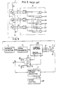
- Fig. 6 shows in detail a driving amplifier 63 constituting the three phase motor control circuit shown in Fig. 5.
- the parts having the same function as those in Fig. 1 are designated by the same reference numerals.
- Reference numerals 12-17 designate switching elements including the PNP transistors 12-14 and the NPN transistors 15-17 for supplying motor driving coils 4 with a current
- the circuit is further provided with a source voltage 18 and an earth voltage 60.
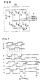
- Fig. 7 shows by way of example the waveforms of the base input signals for the transistors 12-17.
- one of the PNP transistors 12-14 and one of the NPN transistors 15-17 are selectively made conductive to successively supply the motor driving coils 4 one after one with a current to cause the rotor (including a rotor magnet) to rotate.
- the technique is known well and the description with respect therefor will be omitted.
- a method of shorting the counter electromotive force induced in the motor driving coils 4 is employed to obtain a braking effect.
- the braking effect can be obtained during the rotation of the motor.
- the current which flows at this time is not large enough to cause the motor to rotate, it is not required to make the capacity of switching elements greater.
- the motor driving coil 4 inherently has its resistance value in actuality so as to effectively restrict the current caused to flow by the shorting to thereby prevent the coil and transistors from being damaged by an overcurrent.
- the shorting may be performed by making conductive all the NPN transistors 15-17, while maintaining all the PNP transistors 12-14 off, for example, from the time t 1 as shown in Fig. 7.
- at least one of the transistors 15 ⁇ 17 is made to be such a mode that a current flows from its emitter to collector, that is a mode in which a current flows in the direction opposite to that of a normal collector current, to thereby make a path for the shorting current.
- the same effect can be obtained by making conductive all the PNP transistors 12-14, while keeping all the NPN transistors 15-17 off.
- a control circuit for providing the period to produce a control signal for this braking operation in Fig. 5 will be described.
- the same reference numerals as those used in Figs. 1 and 3 denote the parts having the same functions as those shown in Figs. 1 and 3.
- the reference numerals 19 and 20 denote a voltage comparator and a reference voltage source, respectively.
- a speed control circuit 25 as shown in Fig. 5 commands a second speed S 2 and the operation state shifts from the curve 52 to the curve 53 in the frequency v.s. voltage characteristics of the frequency-to-voltage converter 7, as shown in Fig. 9. That is, the output e, of the frequency-to-voltage converter 7 decreases as indicated by a downward arrow in Fig. 8.
- the supply of current to the motor driving coils 4 is stopped by making high the level of base input signals a, b and c to the PNP transistors 12-14 of Fig. 5.
- Fig. 10 the same reference numerals as those used in Figs. 1, 5 and 6 denote the parts having that same functions as those shown in Figs. 1, 5 and 6.
- the reference numerals 21 and 22 denote reference voltage sources respectively
- 23 and 24 denote constant current sources
- 26-39 denote transistors
- 40 ⁇ 44 denote resistors.
- the differential amplifier 8 constituted by the transistors 38 and 39 and the constant current source 23 serves to operate as a control amplifier.
- the input voltage of the terminal 9 is slightly higher than the reference voltage V 1 under normal rotating conditions, and the collector current of the transistor 38 is more than that of the transistor 39.
- a motor current control output is derived from the collector of the transistor 38 to form the current source of a differential switch constituted by the transistors 32-34.
- the voltage comparator 19 constituted by the transistors 35 and 36 and the constant current source 23 serves to operate as a differential amplifier. Since the reference voltage V 82 is set to be below the reference voltage V 81 , and the input voltage of the terminal 9 is higher than the reference voltage V S1 under the normal rotating condition, the transistor 36 turns on and the transistor 35 turns off. At this time, each of the potential of the bases of the transistors 26 ⁇ 28 and 29-31 rises so that these transistors are cut off.
- the transistors 15 ⁇ 17 operate under the control of the signals d, e and f inputted to the bases of them
- the transistors 12-14 operate under the control of the signals a, b and c inputted to the bases of them so as to flow currents through one of the bases of transistors 1214 in turn, controlling the amount of the current flowing into the motor driving coils 4.
- the signals a, b and c are obtained by inverting the signals a, b and c in Fig. 4.
- the conduction state of the transistor 35 becomes deep to cause the transistor 26 ⁇ 28 to be conductive to turn all the transistors 15-17 on.
- the resistors 40 and 41 are provided to prevent the order of occurrence of the abovementioned on/off state from being reversed. For example, these resistors may prevent the simultaneous turning- on of the transistors 12 and 15.
- the control input voltage e comes back to the value V o
- the transistors 12-14 come back to the normally drived state from their off-state after a period of time At 2 has elapsed from the time t 2 at which the transistors 15 ⁇ 17 have come back to the normally drived state.
- the resistors 40 and 41 operate to surely establish the time At 2 ,
- the present invention is advantageous in that it is not required to make greater the capacity of the switching elements at the output stage of braking function for the brushless DC motor and the braking effect can be obtained without causing any problem of insufficient braking which may occur for example in the opposite phase braking operation performed by applying inverted signals, so that, particularly, the response time for the change-over of motor speed from high to low (including a stop) can be reduced.
- the present invention is advantageous also in that the braking effect can be obtained only by providing the above-mentioned braking period at a part of a range of the variations in control input voltage without a complex control.
- switching elements in Fig. 5 operate in the current mode, they may be such transistors which operate in the voltage mode as shown in Fig. 11 or, alternatively, they may be other switching elements such as thyristors.
- a differential amplifier is used for comparing the voltages V 1 with V 2 in the embodiments described above, it may be replaced by any other comparing means.
- any characteristic curve other than that shown in Fig. 8 such as abscissa or zero voltage line may be selected.
Landscapes
- Engineering & Computer Science (AREA)
- Power Engineering (AREA)
- Control Of Motors That Do Not Use Commutators (AREA)
Description
- The present invention relates to a motor driving circuit and particularly to a circuit for driving a capstan motor provided with a braking function for use in a video tape recorder (VTR).
- An example of the conventional driving circuit for a three phase motor is shown in Fig. 1. In the drawing, the reference numeral 1 denotes a rotation position detector for detecting the rotation position of a magnet mounted on a rotor 5 of a three-phase motor by using a conventional contactless sensor such as a Hall element, 2 denotes a signal generator responsive to an output of the rotation position detector 1 for generating a signal for changing over
motor driving coils motor driving coils 4 with a current, 6 denotes an oscillator for generating a signal having a frequency corresponding to the rotation speed of therotor 5, 7 denotes a frequency-to-voltage converter for producing a voltage corresponding to the frequency of the output signal of the oscillator 6, and 8 denotes a control amplifier for controlling the current flowing in themotor driving coils 4 in accordance with the output voltage of the frequency-to-voltage converter 7. The oscillator 6, the frequency-to-voltage converter 7 and the control amplifier 8 constitute a speed control loop. Thesignal generator 2 has a known three-phase driving current generating circuit as shown in Fig. 3. U.S. Patent No. 4,338,554 to Fukushima et al. discloses a frequency-voltage comparator used in such a motor driving circuit. - Generally, in such a motor driving circuit, the relation between the input voltage et and the motor driving current Im,of the combination of the control amplifier 8 and the
current amplifier 3 in the conventional open loop system has been as shown in Fig. 2. The value of voltage from which the motor current 1M begins to flow is determined depending on a reference voltage V1 as shown in Fig. 1. The trial to positively decelerate the rotation speed of the motor has not been considered in the arrangement of Fig. 2, while the applied voltage e, was set below the reference voltage V1 so as to expect only the natural deceleration of the motor due to the rotation load and frictional resistance thereof. The running speed of a tape in the VTR is determined depending on the desired reproducing picture image speed, and the more the number of values of this desired reproducing picture image speed are set, the more the number of changing-over of the speed increases. - In such a conventional motor driving circuit, there has been a disadvantage that in the case where the rotation speed is changed over, particularly when the speed is changed from high to low, it takes very long time for the deceleration due to the inertia moment inherently provided in the motor, resulting in a poor response.
- To improve this disadvantage, it is considered to provide an opposite phase control means for decelerating the motor speed by reversing the direction of the current flowing in the motor driving coils. In this method, however, it is necessary to shorten the reverse signal application period in order to avoid the problem that if the reverse signal application period is long the motor begins to actually reversely rotate, so that a rapid braking effect can not be expected. Further, there is a problem that the maximum current flowing through the switching element is the sum of the currents determined in accordance with the source voltage and the counter electromotive force respectively, resulting in the requirement of a larger capacity for the switching element so as to be able to withstand against a larger current.
- US―A―4 319 171 discloses a motor controlled circuit for a DC-motor according to the generic part of claim 1. This circuit includes a bridge having switching elements disposed in each arm thereof and being adapted for the connection of a motor between pairs of arms. For forming the closed loop two transistors in adjacent arms of the bridge are simultaneously turned on short- circuiting the motor and absorbing the back electromotive force. However, this circuit can be used for small currents in small motors only.
- DE-A-3 117 322 discloses a similar circuit for controlling DC-motors. This circuit includes as well for transistors constituting a bridge between the neutral points of which the DC-motor is disposed. For braking a closed loop is switched by a pair of adjacent transistors absorbing the electromotive force. The circuit is adapted to motors having a driving voltage of approximately 1 V and a current of approximately 50 mA.
- An object of the present invention is to eliminate the above-mentioned disadvantages in the prior art. Another object of the present invention is to provide a motor driving circuit having a braking effect to speed up the change over of the motor speed from high to low (including the stopping mode).
- These objects are solved by the invention as described in claim 1.
- To attain the above-mentioned objects, according to the present invention, braking means is provided in a motor driving stage for providing a braking effect to the counter electromotive force induced in the motor coil by shorting the opposite ends of the motor coil and the above-mentioned braking effect is actuated when the speed control input-voltage is in a predetermined voltage range so as to speed up the response in decelerating control.
- Fig. 1 is a block diagram showing an example of the conventional three-phase motor driving circuit;
- Fig. 2 is a graph showing the characteristic of the control input-voltage v.s. the output current to the
motor driving coils 4; - Fig. 3 is a block diagram showing in detail the
blocks 1 and 2 in Fig. 1; - Fig. 4 shows the waveform of three-phase rotation signal;
- Fig. 5 is a block diagram showing an embodiment of the present invention;
- Fig. 6 is a circuit diagram showing in detail the
block 63 in Fig. 5; - Fig. 7 shows waveforms of signals at main portions in Fig. 6;
- Fig. 8 shows waveforms illustrating the braking operation according to the present invention;
- Fig. 9 is a graph showing the characteristic of the frequency-to-voltage converter;
- Fig. 10 is a circuit diagram showing an embodiment of the present invention; and
- Fig. 11 is a circuit diagram showing another embodiment of the present invention.
- Referring to Figs. 5 to 7, the principle of the present invention will be described.
- Fig. 6 shows in detail a
driving amplifier 63 constituting the three phase motor control circuit shown in Fig. 5. In Fig. 5, the parts having the same function as those in Fig. 1 are designated by the same reference numerals. Reference numerals 12-17 designate switching elements including the PNP transistors 12-14 and the NPN transistors 15-17 for supplyingmotor driving coils 4 with a current The circuit is further provided with asource voltage 18 and anearth voltage 60. Fig. 7 shows by way of example the waveforms of the base input signals for the transistors 12-17. In this embodiment of the driving circuit, one of the PNP transistors 12-14 and one of the NPN transistors 15-17 are selectively made conductive to successively supply themotor driving coils 4 one after one with a current to cause the rotor (including a rotor magnet) to rotate. The technique is known well and the description with respect therefor will be omitted. - According to the present invention, a method of shorting the counter electromotive force induced in the
motor driving coils 4 is employed to obtain a braking effect. In this method, since the counter electromotive force is produced due to the rotation of the motor, the braking effect can be obtained during the rotation of the motor. For this, in the method according to the present invention, there does not occur the above-mentioned disadvantage which is caused in the opposite phase braking method. Further, since the current which flows at this time is not large enough to cause the motor to rotate, it is not required to make the capacity of switching elements greater. Themotor driving coil 4 inherently has its resistance value in actuality so as to effectively restrict the current caused to flow by the shorting to thereby prevent the coil and transistors from being damaged by an overcurrent. - The shorting may be performed by making conductive all the NPN transistors 15-17, while maintaining all the PNP transistors 12-14 off, for example, from the time t1 as shown in Fig. 7. At this time, depending on the state of counter electromotive force, at least one of the
transistors 15―17 is made to be such a mode that a current flows from its emitter to collector, that is a mode in which a current flows in the direction opposite to that of a normal collector current, to thereby make a path for the shorting current. Alternatively, it will be appreciated that the same effect can be obtained by making conductive all the PNP transistors 12-14, while keeping all the NPN transistors 15-17 off. - Next, referring to Figs. 7-9, a control circuit for providing the period to produce a control signal for this braking operation in Fig. 5 will be described. In Fig. 5, the same reference numerals as those used in Figs. 1 and 3 denote the parts having the same functions as those shown in Figs. 1 and 3. The
reference numerals 19 and 20 denote a voltage comparator and a reference voltage source, respectively. When a predetermined speed S1 of rotation is set, a voltage Vo which is a little larger than a reference voltage V1 of a reference voltage source 10 is applied to a control input-voltage terminal 9 and the torque produced in the motor may be controlled, for example, by changing asource voltage 18 in response to an output of a control amplifier 8. When the rotation speed of the motor is changed over from high to low, aspeed control circuit 25 as shown in Fig. 5 commands a second speed S2 and the operation state shifts from thecurve 52 to the curve 53 in the frequency v.s. voltage characteristics of the frequency-to-voltage converter 7, as shown in Fig. 9. That is, the output e, of the frequency-to-voltage converter 7 decreases as indicated by a downward arrow in Fig. 8. At the time t1 at which the value e, downwardly exceeds beyond the voltage V1 of the reference voltage source 10, the supply of current to themotor driving coils 4 is stopped by making high the level of base input signals a, b and c to the PNP transistors 12-14 of Fig. 5. At this time, the period (t1 to t2 in Fig. 7) in which the control input voltage e, is lowered than the reference voltage V2 (V2 ≦ V1) from the reference voltage source 20 is detected by thevoltage comparator 29 which causes abraking circuit 50 to produce control signals (a)-(f) of Fig. 7 for the period from t1 to t2. Referring to Fig. 10, the operation of this control circuit will be described. - In Fig. 10, the same reference numerals as those used in Figs. 1, 5 and 6 denote the parts having that same functions as those shown in Figs. 1, 5 and 6. The
reference numerals 21 and 22 denote reference voltage sources respectively, 23 and 24 denote constant current sources, 26-39 denote transistors, and 40―44 denote resistors. The differential amplifier 8 constituted by thetransistors 38 and 39 and the constantcurrent source 23 serves to operate as a control amplifier. - The input voltage of the terminal 9 is slightly higher than the reference voltage V1 under normal rotating conditions, and the collector current of the transistor 38 is more than that of the
transistor 39. A motor current control output is derived from the collector of the transistor 38 to form the current source of a differential switch constituted by the transistors 32-34. Thevoltage comparator 19 constituted by thetransistors current source 23 serves to operate as a differential amplifier. Since the reference voltage V82 is set to be below the reference voltage V81, and the input voltage of the terminal 9 is higher than the reference voltage VS1 under the normal rotating condition, thetransistor 36 turns on and thetransistor 35 turns off. At this time, each of the potential of the bases of thetransistors 26―28 and 29-31 rises so that these transistors are cut off. So thetransistors 15―17 operate under the control of the signals d, e and f inputted to the bases of them, and the transistors 12-14 operate under the control of the signals a, b and c inputted to the bases of them so as to flow currents through one of the bases oftransistors 1214 in turn, controlling the amount of the current flowing into the motor driving coils 4. The signals a, b and c are obtained by inverting the signals a, b and c in Fig. 4. - The braking of the motor is now described. As described above, when the control input voltage Vµ at the terminal 9 is lowered more than the reference voltage &V1 as indicated by the downward arrow in Fig. 9, the state of the differential amplifier 8 is reversed and the transistor 38 is cut off, so that the transistors 32-34 are cut off and the transistors 12-14 are cut off. When the control input voltage Vo is further lowered to below the reference voltage V2, the
transistor 35 turns on and the state of thedifferential amplifier 19 is reversed. At the first stage of this behavior, the transistors 29-31, by the lowering of the base potential of them, become conductive to turn all the transistors 12-14 off. Accordingly, the supply of the current to the driving coils 4 is stopped. - After a period of time Δt1 as shown in Fig. 7, the conduction state of the
transistor 35 becomes deep to cause thetransistor 26―28 to be conductive to turn all the transistors 15-17 on. Theresistors transistors transistors 15―17 have come back to the normally drived state. Theresistors - The present invention is advantageous in that it is not required to make greater the capacity of the switching elements at the output stage of braking function for the brushless DC motor and the braking effect can be obtained without causing any problem of insufficient braking which may occur for example in the opposite phase braking operation performed by applying inverted signals, so that, particularly, the response time for the change-over of motor speed from high to low (including a stop) can be reduced. The present invention is advantageous also in that the braking effect can be obtained only by providing the above-mentioned braking period at a part of a range of the variations in control input voltage without a complex control.
- Although the switching elements in Fig. 5 operate in the current mode, they may be such transistors which operate in the voltage mode as shown in Fig. 11 or, alternatively, they may be other switching elements such as thyristors. Further, although a differential amplifier is used for comparing the voltages V1 with V2 in the embodiments described above, it may be replaced by any other comparing means. Further, any characteristic curve other than that shown in Fig. 8 such as abscissa or zero voltage line may be selected.
Claims (6)
Applications Claiming Priority (2)
| Application Number | Priority Date | Filing Date | Title |
|---|---|---|---|
| JP51345/82 | 1982-03-31 | ||
| JP57051345A JPH0728553B2 (en) | 1982-03-31 | 1982-03-31 | Motor drive circuit |
Publications (3)
| Publication Number | Publication Date |
|---|---|
| EP0090423A2 EP0090423A2 (en) | 1983-10-05 |
| EP0090423A3 EP0090423A3 (en) | 1984-08-22 |
| EP0090423B1 true EP0090423B1 (en) | 1987-03-04 |
Family
ID=12884334
Family Applications (1)
| Application Number | Title | Priority Date | Filing Date |
|---|---|---|---|
| EP83103177A Expired EP0090423B1 (en) | 1982-03-31 | 1983-03-30 | Motor driving circuit |
Country Status (4)
| Country | Link |
|---|---|
| US (1) | US4494056A (en) |
| EP (1) | EP0090423B1 (en) |
| JP (1) | JPH0728553B2 (en) |
| DE (1) | DE3370106D1 (en) |
Families Citing this family (22)
| Publication number | Priority date | Publication date | Assignee | Title |
|---|---|---|---|---|
| JPS61180594A (en) * | 1984-12-19 | 1986-08-13 | Victor Co Of Japan Ltd | Motor drive circuit |
| JPS62207186A (en) * | 1986-03-06 | 1987-09-11 | Mitsubishi Electric Corp | Disk driving device |
| US4831469A (en) * | 1987-07-29 | 1989-05-16 | International Business Machines Corporation | Disk drive head retract and motor braking method and apparatus |
| JP2536010B2 (en) * | 1988-01-25 | 1996-09-18 | ティアツク株式会社 | 3-phase brushless motor device |
| JP2551836B2 (en) * | 1989-02-28 | 1996-11-06 | 日本電産株式会社 | Drive controller |
| JP2554374B2 (en) * | 1989-07-03 | 1996-11-13 | 株式会社三協精機製作所 | Brushless motor drive circuit |
| DE3923267A1 (en) * | 1989-07-14 | 1991-01-24 | Wap Reinigungssysteme | ELECTRONICALLY COMMUTED MOTOR FOR VACUUM CLEANERS AND THE LIKE |
| DE69028841T2 (en) * | 1990-02-06 | 1997-02-13 | Seagate Technology | Motor brake circuit for use in a magnetic disk drive system |
| US5091680A (en) * | 1990-02-06 | 1992-02-25 | Seagate Technology, Inc. | Motor brake circuit for magnetic disk drive system |
| US6407594B1 (en) | 1993-04-09 | 2002-06-18 | Sgs-Thomson Microelectronics S.R.L. | Zero bias current driver control circuit |
| DE69306764T2 (en) * | 1993-05-31 | 1997-04-10 | Sgs Thomson Microelectronics | Switchable half-bridge discharge time controller using a single capacitor |
| DE4413507A1 (en) * | 1994-04-19 | 1995-10-26 | Sel Alcatel Ag | Process for reversing the direction of rotation of a full-speed brushless DC motor and brushless DC motor |
| ATE205311T1 (en) * | 1995-05-11 | 2001-09-15 | Siemens Ag | SAFE PROCESSING OF SAFETY-RELATED PROCESS SIGNALS |
| JP3473276B2 (en) * | 1996-07-03 | 2003-12-02 | 松下電器産業株式会社 | Inverter device |
| KR100422439B1 (en) * | 1997-01-15 | 2004-05-17 | 페어차일드코리아반도체 주식회사 | Pd limiting circuit for motor driver ic |
| US6118241A (en) * | 1997-11-25 | 2000-09-12 | Kollmorgen Corporation | Dynamic braking system for electric motors |
| FI115393B (en) | 2002-03-28 | 2005-04-29 | Abb Oy | Method and system for braking a propulsion unit engine |
| GB2427359A (en) * | 2005-06-23 | 2006-12-27 | Johnson Electric Sa | Hair dryer with braking device |
| JP5613500B2 (en) * | 2010-08-25 | 2014-10-22 | セミコンダクター・コンポーネンツ・インダストリーズ・リミテッド・ライアビリティ・カンパニー | Motor drive circuit |
| JP5981219B2 (en) * | 2012-05-18 | 2016-08-31 | 株式会社マキタ | Braking device for three-phase brushless motor and electrical equipment |
| JP7674658B2 (en) * | 2021-07-13 | 2025-05-12 | 株式会社今仙電機製作所 | Positioning device and control method thereof |
| JP7674659B2 (en) * | 2021-07-13 | 2025-05-12 | 株式会社今仙電機製作所 | Positioning device and control method thereof |
Family Cites Families (11)
| Publication number | Priority date | Publication date | Assignee | Title |
|---|---|---|---|---|
| DE2106898A1 (en) * | 1971-02-13 | 1972-08-24 | Siemens Ag | Spinning turbine with a speed-controlled, brakable electric drive motor |
| US3895277A (en) * | 1973-05-24 | 1975-07-15 | Sycor Inc | Electronic dynamic braking for tape recorder devices |
| JPS5012764A (en) * | 1973-06-05 | 1975-02-10 | ||
| US3916276A (en) * | 1974-03-28 | 1975-10-28 | Vee Arc Corp | Direct current motor drive |
| JPS5128610A (en) * | 1974-09-04 | 1976-03-11 | Hitachi Ltd | Museiryushimoota no sokudoseigyokairo |
| DE2843622A1 (en) * | 1978-10-06 | 1980-04-17 | Bosch Gmbh Robert | CONTROL DEVICE FOR AN ACTUATOR, ESPECIALLY A ACTUATOR |
| JPS55144788A (en) * | 1979-04-27 | 1980-11-11 | Hitachi Ltd | Automatic gain-control circuit for motor servo-system |
| JPS5620395U (en) * | 1979-07-23 | 1981-02-23 | ||
| JPS5840919B2 (en) * | 1979-08-16 | 1983-09-08 | ファナック株式会社 | Electric motor operation control device |
| US4295170A (en) * | 1979-10-22 | 1981-10-13 | Mike A. Janko | Variable tape speed for video recorders |
| JPS56157289A (en) * | 1980-05-01 | 1981-12-04 | Olympus Optical Co Ltd | Braking device for motor |
-
1982
- 1982-03-31 JP JP57051345A patent/JPH0728553B2/en not_active Expired - Lifetime
-
1983
- 1983-03-30 EP EP83103177A patent/EP0090423B1/en not_active Expired
- 1983-03-30 DE DE8383103177T patent/DE3370106D1/en not_active Expired
- 1983-03-30 US US06/480,372 patent/US4494056A/en not_active Expired - Lifetime
Also Published As
| Publication number | Publication date |
|---|---|
| EP0090423A3 (en) | 1984-08-22 |
| EP0090423A2 (en) | 1983-10-05 |
| US4494056A (en) | 1985-01-15 |
| DE3370106D1 (en) | 1987-04-09 |
| JPS58172992A (en) | 1983-10-11 |
| JPH0728553B2 (en) | 1995-03-29 |
Similar Documents
| Publication | Publication Date | Title |
|---|---|---|
| US4494056A (en) | Motor driving circuit | |
| US3783359A (en) | Brushless d. c. motor using hall generators for commutation | |
| US5481167A (en) | Amplifier and method for detecting the bemf of a coil of a polyphase sensorless DC motor | |
| EP0179484B1 (en) | Current control type driver circuit for brushless motor | |
| EP0814473A2 (en) | Harddisk spindle motor controller with either PWM or linear current control output | |
| JP2547553B2 (en) | Power supply current limiting device for DC motor and electric motor equipped with such limiting device | |
| EP0135128A2 (en) | Stepper motor damping circuit and a method therefor | |
| US5339013A (en) | Method and apparatus for driving a brushless motor including varying the duty cycle in response to variations in the rotational speed | |
| US7421193B2 (en) | Digital motor control system and method | |
| US3876168A (en) | Motor control for tape transport system | |
| US3665500A (en) | Variable mode feedback control system | |
| US3302083A (en) | Variable synchronous motors which rotate at a self-determined rotational speed | |
| US3916441A (en) | Tape transport having variable torque constant reel and capstan drive motor | |
| US4914371A (en) | Apparatus for controlling AC servo motor | |
| US3671837A (en) | Rotation control circuit for transistor motor | |
| US4864211A (en) | Drive control for DC electric motor | |
| Krisbnan et al. | Speed Control of DC Motor Using Teyristor Dual Converter | |
| Kavanagh et al. | Innovative current sensing for brushless DC drives | |
| JP3296706B2 (en) | Motor drive | |
| US2259306A (en) | Electric shovel control | |
| JPH03239185A (en) | Method and apparatus for driving brushless motor | |
| JPH0121717B2 (en) | ||
| KR0137103B1 (en) | A double speed driving method and circuit for switched reluctance motor | |
| JPH02197291A (en) | Method and device for starting brushless motor | |
| JPH04347591A (en) | Driver for synchronous ac servo motor |
Legal Events
| Date | Code | Title | Description |
|---|---|---|---|
| PUAI | Public reference made under article 153(3) epc to a published international application that has entered the european phase |
Free format text: ORIGINAL CODE: 0009012 |
|
| AK | Designated contracting states |
Designated state(s): DE FR GB |
|
| PUAL | Search report despatched |
Free format text: ORIGINAL CODE: 0009013 |
|
| AK | Designated contracting states |
Designated state(s): DE FR GB |
|
| RHK1 | Main classification (correction) |
Ipc: H02P 3/12 |
|
| 17P | Request for examination filed |
Effective date: 19841221 |
|
| GRAA | (expected) grant |
Free format text: ORIGINAL CODE: 0009210 |
|
| AK | Designated contracting states |
Kind code of ref document: B1 Designated state(s): DE FR GB |
|
| REF | Corresponds to: |
Ref document number: 3370106 Country of ref document: DE Date of ref document: 19870409 |
|
| ET | Fr: translation filed | ||
| PLBE | No opposition filed within time limit |
Free format text: ORIGINAL CODE: 0009261 |
|
| STAA | Information on the status of an ep patent application or granted ep patent |
Free format text: STATUS: NO OPPOSITION FILED WITHIN TIME LIMIT |
|
| 26N | No opposition filed | ||
| PGFP | Annual fee paid to national office [announced via postgrant information from national office to epo] |
Ref country code: FR Payment date: 20000131 Year of fee payment: 18 |
|
| PGFP | Annual fee paid to national office [announced via postgrant information from national office to epo] |
Ref country code: GB Payment date: 20000320 Year of fee payment: 18 |
|
| PGFP | Annual fee paid to national office [announced via postgrant information from national office to epo] |
Ref country code: DE Payment date: 20000428 Year of fee payment: 18 |
|
| PG25 | Lapsed in a contracting state [announced via postgrant information from national office to epo] |
Ref country code: GB Free format text: LAPSE BECAUSE OF NON-PAYMENT OF DUE FEES Effective date: 20010330 |
|
| GBPC | Gb: european patent ceased through non-payment of renewal fee |
Effective date: 20010330 |
|
| PG25 | Lapsed in a contracting state [announced via postgrant information from national office to epo] |
Ref country code: FR Free format text: LAPSE BECAUSE OF NON-PAYMENT OF DUE FEES Effective date: 20011130 |
|
| REG | Reference to a national code |
Ref country code: FR Ref legal event code: ST |
|
| PG25 | Lapsed in a contracting state [announced via postgrant information from national office to epo] |
Ref country code: DE Free format text: LAPSE BECAUSE OF NON-PAYMENT OF DUE FEES Effective date: 20020101 |