EP0089559A2 - Method for forming metal coatings for metallurgy patterns on dielectric substrates - Google Patents
Method for forming metal coatings for metallurgy patterns on dielectric substrates Download PDFInfo
- Publication number
- EP0089559A2 EP0089559A2 EP83102357A EP83102357A EP0089559A2 EP 0089559 A2 EP0089559 A2 EP 0089559A2 EP 83102357 A EP83102357 A EP 83102357A EP 83102357 A EP83102357 A EP 83102357A EP 0089559 A2 EP0089559 A2 EP 0089559A2
- Authority
- EP
- European Patent Office
- Prior art keywords
- substrate
- metal
- metal layer
- pattern
- layer
- Prior art date
- Legal status (The legal status is an assumption and is not a legal conclusion. Google has not performed a legal analysis and makes no representation as to the accuracy of the status listed.)
- Granted
Links
Images
Classifications
-
- H—ELECTRICITY
- H01—ELECTRIC ELEMENTS
- H01L—SEMICONDUCTOR DEVICES NOT COVERED BY CLASS H10
- H01L23/00—Details of semiconductor or other solid state devices
- H01L23/48—Arrangements for conducting electric current to or from the solid state body in operation, e.g. leads, terminal arrangements ; Selection of materials therefor
- H01L23/488—Arrangements for conducting electric current to or from the solid state body in operation, e.g. leads, terminal arrangements ; Selection of materials therefor consisting of soldered or bonded constructions
- H01L23/498—Leads, i.e. metallisations or lead-frames on insulating substrates, e.g. chip carriers
- H01L23/49866—Leads, i.e. metallisations or lead-frames on insulating substrates, e.g. chip carriers characterised by the materials
-
- H—ELECTRICITY
- H01—ELECTRIC ELEMENTS
- H01L—SEMICONDUCTOR DEVICES NOT COVERED BY CLASS H10
- H01L21/00—Processes or apparatus adapted for the manufacture or treatment of semiconductor or solid state devices or of parts thereof
- H01L21/02—Manufacture or treatment of semiconductor devices or of parts thereof
- H01L21/04—Manufacture or treatment of semiconductor devices or of parts thereof the devices having at least one potential-jump barrier or surface barrier, e.g. PN junction, depletion layer or carrier concentration layer
- H01L21/48—Manufacture or treatment of parts, e.g. containers, prior to assembly of the devices, using processes not provided for in a single one of the subgroups H01L21/06 - H01L21/326
- H01L21/4814—Conductive parts
- H01L21/4846—Leads on or in insulating or insulated substrates, e.g. metallisation
-
- H—ELECTRICITY
- H05—ELECTRIC TECHNIQUES NOT OTHERWISE PROVIDED FOR
- H05K—PRINTED CIRCUITS; CASINGS OR CONSTRUCTIONAL DETAILS OF ELECTRIC APPARATUS; MANUFACTURE OF ASSEMBLAGES OF ELECTRICAL COMPONENTS
- H05K3/00—Apparatus or processes for manufacturing printed circuits
- H05K3/22—Secondary treatment of printed circuits
- H05K3/24—Reinforcing the conductive pattern
- H05K3/245—Reinforcing conductive patterns made by printing techniques or by other techniques for applying conductive pastes, inks or powders; Reinforcing other conductive patterns by such techniques
- H05K3/246—Reinforcing conductive paste, ink or powder patterns by other methods, e.g. by plating
-
- H—ELECTRICITY
- H01—ELECTRIC ELEMENTS
- H01L—SEMICONDUCTOR DEVICES NOT COVERED BY CLASS H10
- H01L2924/00—Indexing scheme for arrangements or methods for connecting or disconnecting semiconductor or solid-state bodies as covered by H01L24/00
- H01L2924/0001—Technical content checked by a classifier
- H01L2924/0002—Not covered by any one of groups H01L24/00, H01L24/00 and H01L2224/00
-
- H—ELECTRICITY
- H01—ELECTRIC ELEMENTS
- H01L—SEMICONDUCTOR DEVICES NOT COVERED BY CLASS H10
- H01L2924/00—Indexing scheme for arrangements or methods for connecting or disconnecting semiconductor or solid-state bodies as covered by H01L24/00
- H01L2924/095—Indexing scheme for arrangements or methods for connecting or disconnecting semiconductor or solid-state bodies as covered by H01L24/00 with a principal constituent of the material being a combination of two or more materials provided in the groups H01L2924/013 - H01L2924/0715
- H01L2924/097—Glass-ceramics, e.g. devitrified glass
- H01L2924/09701—Low temperature co-fired ceramic [LTCC]
-
- H—ELECTRICITY
- H05—ELECTRIC TECHNIQUES NOT OTHERWISE PROVIDED FOR
- H05K—PRINTED CIRCUITS; CASINGS OR CONSTRUCTIONAL DETAILS OF ELECTRIC APPARATUS; MANUFACTURE OF ASSEMBLAGES OF ELECTRICAL COMPONENTS
- H05K2203/00—Indexing scheme relating to apparatus or processes for manufacturing printed circuits covered by H05K3/00
- H05K2203/11—Treatments characterised by their effect, e.g. heating, cooling, roughening
- H05K2203/1105—Heating or thermal processing not related to soldering, firing, curing or laminating, e.g. for shaping the substrate or during finish plating
-
- H—ELECTRICITY
- H05—ELECTRIC TECHNIQUES NOT OTHERWISE PROVIDED FOR
- H05K—PRINTED CIRCUITS; CASINGS OR CONSTRUCTIONAL DETAILS OF ELECTRIC APPARATUS; MANUFACTURE OF ASSEMBLAGES OF ELECTRICAL COMPONENTS
- H05K3/00—Apparatus or processes for manufacturing printed circuits
- H05K3/02—Apparatus or processes for manufacturing printed circuits in which the conductive material is applied to the surface of the insulating support and is thereafter removed from such areas of the surface which are not intended for current conducting or shielding
- H05K3/04—Apparatus or processes for manufacturing printed circuits in which the conductive material is applied to the surface of the insulating support and is thereafter removed from such areas of the surface which are not intended for current conducting or shielding the conductive material being removed mechanically, e.g. by punching
-
- H—ELECTRICITY
- H05—ELECTRIC TECHNIQUES NOT OTHERWISE PROVIDED FOR
- H05K—PRINTED CIRCUITS; CASINGS OR CONSTRUCTIONAL DETAILS OF ELECTRIC APPARATUS; MANUFACTURE OF ASSEMBLAGES OF ELECTRICAL COMPONENTS
- H05K3/00—Apparatus or processes for manufacturing printed circuits
- H05K3/10—Apparatus or processes for manufacturing printed circuits in which conductive material is applied to the insulating support in such a manner as to form the desired conductive pattern
- H05K3/14—Apparatus or processes for manufacturing printed circuits in which conductive material is applied to the insulating support in such a manner as to form the desired conductive pattern using spraying techniques to apply the conductive material, e.g. vapour evaporation
- H05K3/143—Masks therefor
-
- H—ELECTRICITY
- H05—ELECTRIC TECHNIQUES NOT OTHERWISE PROVIDED FOR
- H05K—PRINTED CIRCUITS; CASINGS OR CONSTRUCTIONAL DETAILS OF ELECTRIC APPARATUS; MANUFACTURE OF ASSEMBLAGES OF ELECTRICAL COMPONENTS
- H05K3/00—Apparatus or processes for manufacturing printed circuits
- H05K3/22—Secondary treatment of printed circuits
- H05K3/24—Reinforcing the conductive pattern
- H05K3/244—Finish plating of conductors, especially of copper conductors, e.g. for pads or lands
Definitions
- the invention relates to a method for selectively coating an existing metallurgical pattern supported on a dielectric substrate with a diverse metal layer.
- MLC multi-layer ceramic
- the punched and printed green sheets are selectively stacked on each other into a laminated substrate assembly, as for example, a stack of 15 to 30 green sheets, and the assembly sintered to integrate the sheets and develop the conductor pattern while removing the binder.
- the resultant fired MLC substrate can then be employed for flip-chip mounting of semiconductor devices which are electrically connected to the internal circuitry of the MLC substrate.
- External contact with the MLC substrate is made by a plurality of I/O pins normally brazed or otherwise mounted to the opposite side of the MLC substrate to the internal circuitry thereof.
- the MLC substrate be formed with vias and lines densified in accordance with the corresponding microminitu- rization of the integrated circuit developments. Such microminiaturization is desirable in order that the package be compatible with the corresponding densified integrated circuit device chips mounted thereon.
- the MLC substrate must be provided on the top surface with many small pads which are capable of making registered electrical contact with corresponding closely spaced semiconductor device terminals, e.g. solder mounds.
- solder mounds In order to more efficiently use the modern integrated circuit technology, as many as possible integrated circuit devices are supported on and interconnected within the MLC substrate.
- MLC substrates require a relatively complex metallurgy on the topside to make electrical connection to integrated circuit devices and to provide engineering change pads, and on the bottom side to make connection to the I/O pads, pins or other type connections.
- green ceramic is sintered there is normally a 17 to 20% shrinkage. Frequently, the shrinkage is not uniform throughout the MLC substrate. Since the substrate is relatively large, and the metallurgy geometry quite small, it is difficult and frequently impossible . to produce a mask for coating protective diverse metals on the substrate metallurgy, that is 17 to 20% smaller than the original substrate that will have all open areas that will coincide or register with the substrate metallurgy. Such a mask is necessary for depositing additional metallurgy metals using conventional masking techniques.
- the original metallurgy pattern on the MLC substrate laminate deposited prior to sintering and comprises a refractory (for example molybdenum) metalliferous paste screened on the laminate sheets.
- the refractory metal e.g. molybdenum, tungsten, etc.
- the refractory metal must not only be protectively covered with different metals, as for example nickel, chromium, copper, gold, etc., but also to facilitate the making of connections, as by soldering, to semiconductor devices, compression bonding to wires and/or brazing to I/O pins.
- the protective coating of the refractive MLC substrate metallurgy, where molybdenum is employed is important, since molybdenum is susceptible to reactive corrosion when exposed to humidity of any pH value at operating potentials common in MLC module or substrate applications. This corrosion interrupts conductors, and leads to module failure.
- One method of protecting the substrate metallurgy is by covering them with diverse metals, e.g. nickel, by electroless plating techniques which do not require masks.
- coatings may contain impurities such as phosphorous boron, etc., which may be objectionable in subsequent joining (e.g. soldering, brazing, compression bonding, etc.).
- the protective metal layers can also be deposited by electroplating techniques. However, such plating techniques require electrical connection to each area to be plated, whereas in MLC substrates such connections are not always available, since some pads or portions of the metallurgy pattern can be "electrically floating".
- the inventive method does not have the drawbacks of the electroless selective plating methods, nor the restrictions of the electrochemical selective plating methods.
- the inventive method is particularly useful in coating a protective metal on a refractive metal conductive pattern on ceramic substrate carriers employed for mounting semiconductor devices thereon.
- the inventive method replaces the electroless plating technique for coating nickel on molybdenum metallurgy pattern on ceramic substrate carriers employed for mounting semiconductor devices thereon.
- this invention provides a maskless technique for replacing electroless and electroplating approaches of coating protective metallization on existing metallurgy supported on a dielectric substrate, by blanket coating, e.g. evaporation, sputtering, etc., a protective metallization over a dielectric substrate having on existing diverse metallurgy pattern, heating to diffuse the protective metallization into the existing metallurgy, cooling the substrate to disrupt or spall the protective metal on the non-metallized portions of the substrate, and mechanically removing the protective metallization, preferably ultrasonically, from the substrate surfaces.
- blanket coating e.g. evaporation, sputtering, etc.
- a protective metallization over a dielectric substrate having on existing diverse metallurgy pattern
- heating to diffuse the protective metallization into the existing metallurgy cooling the substrate to disrupt or spall the protective metal on the non-metallized portions of the substrate, and mechanically removing the protective metallization, preferably ultrasonically, from the substrate surfaces.
- the substrate is blanket coated with a protective metal, e.g. nickel, heated to diffuse nickel into the refractory metal, e.g. molybdenum, cooled to disrupt or spall the metal on the ceramic surface, with removal of the protective metallization (e.g. ultrasonically) from the ceramic surfaces.
- a protective metal e.g. nickel
- the protective metallization e.g. ultrasonically
- the nickel layer can be further blanket coated with a passivating metal, e.g. gold, as by sputtering, whereby the nickel and gold will interdiffuse concurrently with the nickel diffusion into the molybdenum metallurgy on heating.
- a passivating metal e.g. gold
- both are blanket coated, as by sputtering with from about 3 to about 7 microns of nickel, a gold film of about 0.25 to 0.5 microns thickness can be sputtered over the nickel layer, which on heating will effect simultaneous Ni-Mo and Ni-Au interdiffusions at temperatures below 750°C.
- the upper limit to Ni-Au diffusion is set by the need to ensure the formation of an oxidation resistant gold- rich Au-Ni solid solution. This is assured below 750°C by the existance of the immiscibility dome in the Au-Ni phase diagram.
- the advantage of this variation lies in the fact that it provides for maskless cladding of the molybdenum circuit features of the alumina MLC substrate with a nickel film rich in gold at its surface essentially similar to the cap structures heretofore obtained by electroless nickel plating followed by gold plating and gold diffusion techniques.
- a fired ceramic substrate 1 typically a multi-layer ceramic structure which can be produced by the method described in US Patent 3 518 756.
- Figs. 1 to 4 are illustrated in broken section, the internal metallurgical pattern in the substrate is not shown since it does not constitute a material part of this invention, which is directed to the treatment of existing exposed metallurgy 2 at the surfaces of substrate 1.
- substrate 1 need not be a multi-layer structure, but could be solid with the metallurgical pattern 2 formed entirely on the surface thereof.
- the metallurgical pattern 2 can be disposed on more than one surface of the substrate, e.g.
- the existing metallurgical pattern cannot only be provided on the top surface of substrate 1 for electrical connection to terminal of a semiconductor device solder mounted thereto, but also extend to and at the opposite bottom surface of substrate 1 for securing thereto of I/O pins.
- the metallurgy 2 has been shown as extending in a raised pattern on substrate 1, it can also constitute the exposed portions 3 of via metallurgy 4.
- the material of present conventional substrates is normally formed of alumina, or alumina plus other materials (e.g. glass) such as described in US Patent 3 540 894.
- the depicted metallurgical pattern 2, shown on the surface of substrate 1 can be formed of a refractory metal, typically molybdenum, which was deposited prior to sintering.
- the substrate 1 is blanket coated by any suitable technique (as by vacuum deposition, sputtering and the like) with a diverse protective metal layer 5, illustratively to a thickness of about 3 to about 7 microns,( 4 m), which can be diffused into the existing metallurgy 2 to thereby selectively increase the adherence to the metallurgical circuit features. On deposition the metal will also be adhered to the substrate surfaces.
- a presently preferred metal is nickel to conform to its present day use by immediate replacement of the current electroless and electro plating operations.
- the blanket coated structure of Fig. 2 is heated to a temperature (below the melting points of the metals) to induce interdiffusion of the metals at the interface therebetween, e.g. the diffusion of the protective metal 5 into the existing metallurgical pattern 2.
- a temperature below the melting points of the metals
- the protective metal 5 into the existing metallurgical pattern 2.
- a thickness of 5 ⁇ m of nickel as a protective coating 5 and molybdenum based metal for the existing metallurgy adequate diffusion of nickel into the molybdenum was obtained with a heat treatment of 5 minutes at temperatures from 650°C to 1100°C.
- the resultant diffused region 6 is shown in Fig. 3.
- This heat treatment is for the purpose of diffusion bonding of the protective metal film 5 to circuit features of the preexisting metallurgical pattern 2, and the sintering of the deposited film 5 of relatively open grain structure to obtain a good lateral adhesion in the film, and to facilitate its removal from the non-metallized or bare surfaces of the substrate.
- Preconditioning of substrate 1 for the debonding or delamination of the initially adherent protective film 5 from the bare surfaces of substrate is obtained during cooling thereof, as a result of the stresses induced by the differential in the thermal contraction coefficients of the metal film 5 and the dielectric composition, which disrupts or spalls the metal film 5 on the bare surfaces of the substrate.
- the metal film 5 is rendered non-adhering to the bare substrate surface, and at this point can be mechanically removed, preferably by subjecting it to an ultrasonic cleaning operation in water or other suitable medium, in conventional tank type ultrasonic cleaners having side and/or bottom mounted transducers.
- the mechanism of film removal in ultrasonic cleaning involves the rupturing of the loose metal film 5 from the substrate areas by the action of the shock waves impinging on the surfaces. The shock waves being induced by bubble collapse (cavitation) within the liquid medium during the ultrasonic action.
- One preferred form of removing the metal film 5 is by use of an ultrasonic horn to focus and deliver very high local intensities of energy (about 100 watts per cm 2 ) and by utilizing the near field characteristics of the ultrasonic field close (e.g. about 1 to about 10 mm) to the horn surface where cavitation plays only a minor role. Under such conditions, the removal of the loosely adherent metal films 5 from the substrate surface is very efficient. For example, non-adhering nickel films of sum thickness can be removed from alumina ceramic surfaces in about 5 to about 30 seconds.
- the mechanism of metal film removal is as follows: In the near-field region, there exists a coupling of the ultrasonic field (generated by the transducer) to the surface of the substrate carrying the metal film. Where the metal film 5 is strongly adhering to the substrate, such as in areas of the preexisting metallurgical circuit features under the film, the ultrasonic energy is merely transmitted through the metal film 5 into the substrate and dissipated. Where the metal film 5 is non-adhering, such as on the bare substrate surface areas, the ultrasonic energy is substantially absorbed by the thin metal film 5, causing it to vibrate with the field. This vibration generates alternating stresses at points of the film where it adheres to the substrate which eventually causes the film breakage at these points.
- High frequencies (e.g. 10-40 KHz) of the field ensures that from 10-40 X 10 3 cycles of alternating stress is applied to the metal film 5 at the boundaries of adhering regions so that the fatigue limit for the film is reached in 1 to 30 seconds depending on the nature of the metal film, its thicknesses, and the distance between adjacent adhering areas.
- the present invention can also accommodate the inclusion of passivating metal films for the protective film, e.g. gold plating of the protective nickel film 5, if the nickel cladding is carried out at diffusion temperatures not exceeding about 750°C, well within the Au-Ni immiscibility dome.
- This can be accomplished by depositing (e.g. vacuum evaporation, sputtering, and the like) a film 10 of gold (0.25 to 0.5 ⁇ m) on top of the deposited nickel film 5 (as shown in Fig. 2A) and carrying out the simultaneous Ni-Mo and Au - Ni solid solution, e.g. 6 and 11 of Figs. 3A and 4A. This is assured below 750°C by the existance of the immiscibility dome in the Au-Ni phase diagram.
- the substrate is preconditioned for ultrasonic removal of the nickel/gold films 5/10 from the bare surfaces of the substrate 1 to produce a structure such as shown in Fig. 4A.
- the advantage of this variation of the processing of this invention lies in the fact that it provides for the maskless cladding of molybdenum circuit features of an alumina MLC substrate with a nickel film rich in gold at its surface, which is essentially similar to the cap structures conventionally obtained by electroless plating followed by gold plating and gold diffusion treatment.
Abstract
Description
- The invention relates to a method for selectively coating an existing metallurgical pattern supported on a dielectric substrate with a diverse metal layer.
- The multi-layer ceramic (MLC) technology for fabricating dielectric substrate carriers for integrated circuit/semiconductor package assemblies is well known. Such MLC substrates are produced by preparing a slurry of a suitable ceramic particulates (e.g. alumina), a fugitive resin binder material, a solvent for the resin binder, normally with an included plasticizer; doctor blading the slurry on removable base with subsequent drying to form thin flexible sheets commonly termed ceramic green sheets. The sheets are then punched to form via holes, and the via holes filled with conductive metalliferous (e.g. molybdenum) paste which is also formed into a pattern of conductive lines which will ultimately form the internal circuitry of the MLC. The punched and printed green sheets are selectively stacked on each other into a laminated substrate assembly, as for example, a stack of 15 to 30 green sheets, and the assembly sintered to integrate the sheets and develop the conductor pattern while removing the binder. The resultant fired MLC substrate can then be employed for flip-chip mounting of semiconductor devices which are electrically connected to the internal circuitry of the MLC substrate.
- External contact with the MLC substrate is made by a plurality of I/O pins normally brazed or otherwise mounted to the opposite side of the MLC substrate to the internal circuitry thereof. It is desirable that the MLC substrate be formed with vias and lines densified in accordance with the corresponding microminitu- rization of the integrated circuit developments. Such microminiaturization is desirable in order that the package be compatible with the corresponding densified integrated circuit device chips mounted thereon. In such application the MLC substrate must be provided on the top surface with many small pads which are capable of making registered electrical contact with corresponding closely spaced semiconductor device terminals, e.g. solder mounds. In order to more efficiently use the modern integrated circuit technology, as many as possible integrated circuit devices are supported on and interconnected within the MLC substrate. Such an arrangement keeps the distances between interconnected devices small and thereby minimizes the time it takes for electrical signals to travel between the interrelated devices. Also this reduces the number of electrical connections which must be made thereby reducing the .cost of the package and increases reliability. The end result is a highly complex MLC package with a lot of small internal printed circuitry contained in a substrate carrier capable of mounting large numbers of integrated circuit devices.
- Further, such MLC substrates require a relatively complex metallurgy on the topside to make electrical connection to integrated circuit devices and to provide engineering change pads, and on the bottom side to make connection to the I/O pads, pins or other type connections. When green ceramic is sintered there is normally a 17 to 20% shrinkage. Frequently, the shrinkage is not uniform throughout the MLC substrate. Since the substrate is relatively large, and the metallurgy geometry quite small, it is difficult and frequently impossible . to produce a mask for coating protective diverse metals on the substrate metallurgy, that is 17 to 20% smaller than the original substrate that will have all open areas that will coincide or register with the substrate metallurgy. Such a mask is necessary for depositing additional metallurgy metals using conventional masking techniques. Usually the original metallurgy pattern on the MLC substrate laminate deposited prior to sintering and comprises a refractory (for example molybdenum) metalliferous paste screened on the laminate sheets. After sintering, the refractory metal (e.g. molybdenum, tungsten, etc.) must not only be protectively covered with different metals, as for example nickel, chromium, copper, gold, etc., but also to facilitate the making of connections, as by soldering, to semiconductor devices, compression bonding to wires and/or brazing to I/O pins. The protective coating of the refractive MLC substrate metallurgy, where molybdenum is employed is important, since molybdenum is susceptible to reactive corrosion when exposed to humidity of any pH value at operating potentials common in MLC module or substrate applications. This corrosion interrupts conductors, and leads to module failure.
- One method of protecting the substrate metallurgy is by covering them with diverse metals, e.g. nickel, by electroless plating techniques which do not require masks. However, such coatings may contain impurities such as phosphorous boron, etc., which may be objectionable in subsequent joining (e.g. soldering, brazing, compression bonding, etc.).
- The protective metal layers can also be deposited by electroplating techniques. However, such plating techniques require electrical connection to each area to be plated, whereas in MLC substrates such connections are not always available, since some pads or portions of the metallurgy pattern can be "electrically floating".
- These electroless and electroplating techniques are expensive time consuming and difficult to control; and thus there is a need for a maskless plating technique which is simple with elimination of processing steps as well as having a significant improvement in yield without problems of phosphorous and/or boron contamination.
- It is the object of the invention to provide a maskless, clean method for selectively metal coating an existing metallurgical pattern on a dielectric substrate with a diverse metal.
- This object is achieved by a method as designed at the beginning of this specification, with the features of the characterizing part of claim 1.
- The inventive method does not have the drawbacks of the electroless selective plating methods, nor the restrictions of the electrochemical selective plating methods. The inventive method is particularly useful in coating a protective metal on a refractive metal conductive pattern on ceramic substrate carriers employed for mounting semiconductor devices thereon. Advantageously the inventive method replaces the electroless plating technique for coating nickel on molybdenum metallurgy pattern on ceramic substrate carriers employed for mounting semiconductor devices thereon.
- Other advantageous embodiments of the inventive sputtering system and its inventive applications are disclosed in the subclaims.
- The invention will become more apparent from the following detailed description taken in conjunction with the accompanying drawings. In the drawings
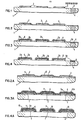
- Figs. 1 show schematically in cross-sectional views, to 4 and broken section, various stages of the method of this invention.
- Figs. 2A show schematic cross-sectional view of a to 4A variation of the method of a further structure in accordance with this invention.
- In its broadest context, this invention provides a maskless technique for replacing electroless and electroplating approaches of coating protective metallization on existing metallurgy supported on a dielectric substrate, by blanket coating, e.g. evaporation, sputtering, etc., a protective metallization over a dielectric substrate having on existing diverse metallurgy pattern, heating to diffuse the protective metallization into the existing metallurgy, cooling the substrate to disrupt or spall the protective metal on the non-metallized portions of the substrate, and mechanically removing the protective metallization, preferably ultrasonically, from the substrate surfaces.
- In specific application to the semiconductor art utilizing alumina MLC substrates with an existing refractory metal, e.g. molybdenum, pattern, the substrate is blanket coated with a protective metal, e.g. nickel, heated to diffuse nickel into the refractory metal, e.g. molybdenum, cooled to disrupt or spall the metal on the ceramic surface, with removal of the protective metallization (e.g. ultrasonically) from the ceramic surfaces.
- With illustrative reference to the application to the fabrication of support carriers or modules for mounting semiconductor devices which employs alumina MLC substrates with an existing molybdenum based metallurgy pattern protectively coated with nickel based metallization in accordance with this invention, it is noted that during post-diffusion cooling of the MLC substrate, the differential thermal contractions of the nickel film and the ceramic body set up stresses that cause the nickel/ceramic adhesion to be completely disrupted. Upon ultrasonic treatment, the loose nickel film on the ceramic is removed leaving a ceramic substrate .surface where only the molybdenum circuit features will remain coated with an adherent nickel coating.
- Where processing considerations require passivation of the nickel cladding with another diverse metal, such as gold, such passivation can be effected concurrently with the diffusion of nickel into the molybdenum metallurgy. In this respect, prior to the diffusion step, the nickel layer can be further blanket coated with a passivating metal, e.g. gold, as by sputtering, whereby the nickel and gold will interdiffuse concurrently with the nickel diffusion into the molybdenum metallurgy on heating. This can be attained if the nickel cladding process can be carried out at diffusion temperatures not exceeding about 750°C, well within the Au-Ni immiscibility dome. In an illustrative example employing molybdenum circuit features of an alumina MLC, both are blanket coated, as by sputtering with from about 3 to about 7 microns of nickel, a gold film of about 0.25 to 0.5 microns thickness can be sputtered over the nickel layer, which on heating will effect simultaneous Ni-Mo and Ni-Au interdiffusions at temperatures below 750°C. The upper limit to Ni-Au diffusion is set by the need to ensure the formation of an oxidation resistant gold- rich Au-Ni solid solution. This is assured below 750°C by the existance of the immiscibility dome in the Au-Ni phase diagram.
- The advantage of this variation lies in the fact that it provides for maskless cladding of the molybdenum circuit features of the alumina MLC substrate with a nickel film rich in gold at its surface essentially similar to the cap structures heretofore obtained by electroless nickel plating followed by gold plating and gold diffusion techniques.
- Although the invention has been referenced specifically to the passivation of molybdenum circuit features of alumina MLC's employed for semiconductor device packaging applications, it is to be understood that the scope of this invention is not to be limited thereto, nor restricted to nickel coatings nor restricted to applications involving MLC substrates. This invention is comprehended for other applications such as decorative metal cladding, glass-to-metal or ceramic-to-metal sealing, as well as to other applications wherein the concept of selective metallization involving diffusion bonding of a deposited metal film selectively to metal features embedded in glass or ceramic with concurrent spalling of the deposited film from the glass or ceramic surface followed by ultrasonic removal of the non-adhering films from the ceramic or glass surfaces. Referring to Fig. 1, there is depicted a fired ceramic substrate 1, typically a multi-layer ceramic structure which can be produced by the method described in US
Patent 3 518 756. Although Figs. 1 to 4 are illustrated in broken section, the internal metallurgical pattern in the substrate is not shown since it does not constitute a material part of this invention, which is directed to the treatment of existing exposedmetallurgy 2 at the surfaces of substrate 1. However, it is to be understood that substrate 1 need not be a multi-layer structure, but could be solid with themetallurgical pattern 2 formed entirely on the surface thereof. Also, it is noted that themetallurgical pattern 2 can be disposed on more than one surface of the substrate, e.g. in MLC structures the existing metallurgical pattern cannot only be provided on the top surface of substrate 1 for electrical connection to terminal of a semiconductor device solder mounted thereto, but also extend to and at the opposite bottom surface of substrate 1 for securing thereto of I/O pins. Also, although themetallurgy 2 has been shown as extending in a raised pattern on substrate 1, it can also constitute the exposedportions 3 of via metallurgy 4. - The material of present conventional substrates is normally formed of alumina, or alumina plus other materials (e.g. glass) such as described in US
Patent 3 540 894. The depictedmetallurgical pattern 2, shown on the surface of substrate 1 can be formed of a refractory metal, typically molybdenum, which was deposited prior to sintering. - As shown in Fig. 2, the substrate 1 is blanket coated by any suitable technique (as by vacuum deposition, sputtering and the like) with a diverse protective metal layer 5, illustratively to a thickness of about 3 to about 7 microns,(4m), which can be diffused into the existing
metallurgy 2 to thereby selectively increase the adherence to the metallurgical circuit features. On deposition the metal will also be adhered to the substrate surfaces. Although various protective metals, such as gold, chrome and the like can be used, a presently preferred metal is nickel to conform to its present day use by immediate replacement of the current electroless and electro plating operations. - In the next operation, the blanket coated structure of Fig. 2 is heated to a temperature (below the melting points of the metals) to induce interdiffusion of the metals at the interface therebetween, e.g. the diffusion of the protective metal 5 into the existing
metallurgical pattern 2. Utilizing a thickness of 5µm of nickel as a protective coating 5 and molybdenum based metal for the existing metallurgy, adequate diffusion of nickel into the molybdenum was obtained with a heat treatment of 5 minutes at temperatures from 650°C to 1100°C. The resultant diffusedregion 6 is shown in Fig. 3. - This heat treatment is for the purpose of diffusion bonding of the protective metal film 5 to circuit features of the preexisting
metallurgical pattern 2, and the sintering of the deposited film 5 of relatively open grain structure to obtain a good lateral adhesion in the film, and to facilitate its removal from the non-metallized or bare surfaces of the substrate. - Preconditioning of substrate 1 for the debonding or delamination of the initially adherent protective film 5 from the bare surfaces of substrate is obtained during cooling thereof, as a result of the stresses induced by the differential in the thermal contraction coefficients of the metal film 5 and the dielectric composition, which disrupts or spalls the metal film 5 on the bare surfaces of the substrate.
- On cooling, the metal film 5 is rendered non-adhering to the bare substrate surface, and at this point can be mechanically removed, preferably by subjecting it to an ultrasonic cleaning operation in water or other suitable medium, in conventional tank type ultrasonic cleaners having side and/or bottom mounted transducers. The mechanism of film removal in ultrasonic cleaning involves the rupturing of the loose metal film 5 from the substrate areas by the action of the shock waves impinging on the surfaces. The shock waves being induced by bubble collapse (cavitation) within the liquid medium during the ultrasonic action. One preferred form of removing the metal film 5 is by use of an ultrasonic horn to focus and deliver very high local intensities of energy (about 100 watts per cm2) and by utilizing the near field characteristics of the ultrasonic field close (e.g. about 1 to about 10 mm) to the horn surface where cavitation plays only a minor role. Under such conditions, the removal of the loosely adherent metal films 5 from the substrate surface is very efficient. For example, non-adhering nickel films of sum thickness can be removed from alumina ceramic surfaces in about 5 to about 30 seconds.
- It is believed that the mechanism of metal film removal is as follows: In the near-field region, there exists a coupling of the ultrasonic field (generated by the transducer) to the surface of the substrate carrying the metal film. Where the metal film 5 is strongly adhering to the substrate, such as in areas of the preexisting metallurgical circuit features under the film, the ultrasonic energy is merely transmitted through the metal film 5 into the substrate and dissipated. Where the metal film 5 is non-adhering, such as on the bare substrate surface areas, the ultrasonic energy is substantially absorbed by the thin metal film 5, causing it to vibrate with the field. This vibration generates alternating stresses at points of the film where it adheres to the substrate which eventually causes the film breakage at these points. High frequencies (e.g. 10-40 KHz) of the field ensures that from 10-40
X 103 cycles of alternating stress is applied to the metal film 5 at the boundaries of adhering regions so that the fatigue limit for the film is reached in 1 to 30 seconds depending on the nature of the metal film, its thicknesses, and the distance between adjacent adhering areas. With the complete removal of the non-adhering metal film 5 from the substrate surfaces, only the pre- existing metallurgical circuit features 2A on the substrate will retain anadherent metal film 6/2A, as shown in Fig. 4. - The present invention can also accommodate the inclusion of passivating metal films for the protective film, e.g. gold plating of the protective nickel film 5, if the nickel cladding is carried out at diffusion temperatures not exceeding about 750°C, well within the Au-Ni immiscibility dome. This can be accomplished by depositing (e.g. vacuum evaporation, sputtering, and the like) a
film 10 of gold (0.25 to 0.5 µm) on top of the deposited nickel film 5 (as shown in Fig. 2A) and carrying out the simultaneous Ni-Mo and Au-Ni solid solution, e.g. 6 and 11 of Figs. 3A and 4A. This is assured below 750°C by the existance of the immiscibility dome in the Au-Ni phase diagram. - As above, on cooling, the substrate is preconditioned for ultrasonic removal of the nickel/gold films 5/10 from the bare surfaces of the substrate 1 to produce a structure such as shown in Fig. 4A.
- The advantage of this variation of the processing of this invention lies in the fact that it provides for the maskless cladding of molybdenum circuit features of an alumina MLC substrate with a nickel film rich in gold at its surface, which is essentially similar to the cap structures conventionally obtained by electroless plating followed by gold plating and gold diffusion treatment.
Claims (9)
Applications Claiming Priority (2)
| Application Number | Priority Date | Filing Date | Title |
|---|---|---|---|
| US06/359,444 US4442137A (en) | 1982-03-18 | 1982-03-18 | Maskless coating of metallurgical features of a dielectric substrate |
| US359444 | 1982-03-18 |
Publications (3)
| Publication Number | Publication Date |
|---|---|
| EP0089559A2 true EP0089559A2 (en) | 1983-09-28 |
| EP0089559A3 EP0089559A3 (en) | 1985-05-22 |
| EP0089559B1 EP0089559B1 (en) | 1988-10-19 |
Family
ID=23413812
Family Applications (1)
| Application Number | Title | Priority Date | Filing Date |
|---|---|---|---|
| EP83102357A Expired EP0089559B1 (en) | 1982-03-18 | 1983-03-10 | Method for forming metal coatings for metallurgy patterns on dielectric substrates |
Country Status (5)
| Country | Link |
|---|---|
| US (1) | US4442137A (en) |
| EP (1) | EP0089559B1 (en) |
| JP (1) | JPS58164249A (en) |
| CA (1) | CA1189748A (en) |
| DE (1) | DE3378288D1 (en) |
Cited By (9)
| Publication number | Priority date | Publication date | Assignee | Title |
|---|---|---|---|---|
| EP0180091A2 (en) * | 1984-10-30 | 1986-05-07 | International Business Machines Corporation | Method of selectively depositing metal layers on a substrate |
| EP0203423A1 (en) * | 1985-05-17 | 1986-12-03 | International Business Machines Corporation | Process for forming a metallurgical system comprising a bottom layer of nickel and a top layer of gold |
| EP0445881A1 (en) * | 1990-03-09 | 1991-09-11 | Koninklijke Philips Electronics N.V. | Method of manufacturing conductor tracks |
| EP0462700A2 (en) * | 1990-05-21 | 1991-12-27 | Motorola, Inc. | Process for the selective encapsulation of an electrically conductive structure in a semiconductor device |
| GB2245596A (en) * | 1990-07-03 | 1992-01-08 | Samsung Electronics Co Ltd | A method for forming a metal layer in a semiconductor device |
| US5266521A (en) * | 1991-03-20 | 1993-11-30 | Samsung Electronics Co., Ltd. | Method for forming a planarized composite metal layer in a semiconductor device |
| EP0689246A1 (en) * | 1994-05-27 | 1995-12-27 | Texas Instruments Incorporated | Improvements in or relating to semiconductor devices |
| GB2297981A (en) * | 1995-02-20 | 1996-08-21 | Matsushita Electric Ind Co Ltd | Method for forming a gold plated electrode |
| US5786624A (en) * | 1994-06-07 | 1998-07-28 | Texas Instruments Incorporated | Dual masking for selective gap fill of submicron interconnects |
Families Citing this family (28)
| Publication number | Priority date | Publication date | Assignee | Title |
|---|---|---|---|---|
| EP0092971B1 (en) * | 1982-04-27 | 1989-08-16 | Richardson Chemical Company | Process for selectively depositing a nickel-boron coating over a metallurgy pattern on a dielectric substrate and products produced thereby |
| US4536470A (en) * | 1982-09-07 | 1985-08-20 | International Business Machines Corporation | Method and apparatus for making a mask conforming to a ceramic substrate metallization pattern |
| JPS5980700A (en) * | 1983-09-14 | 1984-05-10 | Tsunematsu Takemoto | Separation of gynosaponin |
| US4526859A (en) * | 1983-12-12 | 1985-07-02 | International Business Machines Corporation | Metallization of a ceramic substrate |
| US4521449A (en) * | 1984-05-21 | 1985-06-04 | International Business Machines Corporation | Process for forming a high density metallurgy system on a substrate and structure thereof |
| US4552615A (en) * | 1984-05-21 | 1985-11-12 | International Business Machines Corporation | Process for forming a high density metallurgy system on a substrate and structure thereof |
| US4732780A (en) * | 1985-09-26 | 1988-03-22 | General Electric Company | Method of making hermetic feedthrough in ceramic substrate |
| US4833039A (en) * | 1985-09-26 | 1989-05-23 | General Electric Company | Hermetic feedthrough in ceramic substrate |
| US4684446A (en) * | 1985-09-26 | 1987-08-04 | General Electric Company | Secondary metallization by glass displacement in ceramic substrate |
| US4664942A (en) * | 1986-02-05 | 1987-05-12 | General Electric Company | Nickel diffusion bonded to metallized ceramic body and method |
| US4663186A (en) * | 1986-04-24 | 1987-05-05 | International Business Machines Corporation | Screenable paste for use as a barrier layer on a substrate during maskless cladding |
| US4704304A (en) * | 1986-10-27 | 1987-11-03 | International Business Machines Corporation | Method for repair of opens in thin film lines on a substrate |
| US4829020A (en) * | 1987-10-23 | 1989-05-09 | The United States Of America As Represented By The United States Department Of Energy | Substrate solder barriers for semiconductor epilayer growth |
| US5787578A (en) * | 1996-07-09 | 1998-08-04 | International Business Machines Corporation | Method of selectively depositing a metallic layer on a ceramic substrate |
| US6127268A (en) * | 1997-06-11 | 2000-10-03 | Micronas Intermetall Gmbh | Process for fabricating a semiconductor device with a patterned metal layer |
| DE19724595A1 (en) * | 1997-06-11 | 1998-12-17 | Micronas Semiconductor Holding | Structured metal layer production especially on MOS structure |
| US6634543B2 (en) * | 2002-01-07 | 2003-10-21 | International Business Machines Corporation | Method of forming metallic z-interconnects for laminate chip packages and boards |
| US7015064B1 (en) | 2004-04-23 | 2006-03-21 | National Semiconductor Corporation | Marking wafers using pigmentation in a mounting tape |
| US6972244B1 (en) * | 2004-04-23 | 2005-12-06 | National Semiconductor Corporation | Marking semiconductor devices through a mount tape |
| US7135385B1 (en) | 2004-04-23 | 2006-11-14 | National Semiconductor Corporation | Semiconductor devices having a back surface protective coating |
| US7101620B1 (en) | 2004-09-07 | 2006-09-05 | National Semiconductor Corporation | Thermal release wafer mount tape with B-stage adhesive |
| JP2006080424A (en) * | 2004-09-13 | 2006-03-23 | Matsushita Electric Ind Co Ltd | Wiring board and its manufacturing method |
| US8030138B1 (en) | 2006-07-10 | 2011-10-04 | National Semiconductor Corporation | Methods and systems of packaging integrated circuits |
| US7749809B2 (en) * | 2007-12-17 | 2010-07-06 | National Semiconductor Corporation | Methods and systems for packaging integrated circuits |
| US8048781B2 (en) * | 2008-01-24 | 2011-11-01 | National Semiconductor Corporation | Methods and systems for packaging integrated circuits |
| US20100015329A1 (en) * | 2008-07-16 | 2010-01-21 | National Semiconductor Corporation | Methods and systems for packaging integrated circuits with thin metal contacts |
| US8709957B2 (en) | 2012-05-25 | 2014-04-29 | International Business Machines Corporation | Spalling utilizing stressor layer portions |
| JP5778654B2 (en) * | 2012-12-19 | 2015-09-16 | 日本特殊陶業株式会社 | Ceramic substrate and manufacturing method thereof |
Citations (2)
| Publication number | Priority date | Publication date | Assignee | Title |
|---|---|---|---|---|
| US3698941A (en) * | 1969-09-26 | 1972-10-17 | Philips Corp | Method of applying contacts to a semiconductor body |
| US3736167A (en) * | 1971-04-01 | 1973-05-29 | Coors Porcelain Co | Electroless nickel plating process |
Family Cites Families (3)
| Publication number | Priority date | Publication date | Assignee | Title |
|---|---|---|---|---|
| NL7117429A (en) * | 1971-12-18 | 1973-06-20 | ||
| US4206254A (en) * | 1979-02-28 | 1980-06-03 | International Business Machines Corporation | Method of selectively depositing metal on a ceramic substrate with a metallurgy pattern |
| US4232059A (en) * | 1979-06-06 | 1980-11-04 | E-Systems, Inc. | Process of defining film patterns on microelectronic substrates by air abrading |
-
1982
- 1982-03-18 US US06/359,444 patent/US4442137A/en not_active Expired - Lifetime
- 1982-11-19 JP JP57202206A patent/JPS58164249A/en active Granted
-
1983
- 1983-01-17 CA CA000419631A patent/CA1189748A/en not_active Expired
- 1983-03-10 EP EP83102357A patent/EP0089559B1/en not_active Expired
- 1983-03-10 DE DE8383102357T patent/DE3378288D1/en not_active Expired
Patent Citations (2)
| Publication number | Priority date | Publication date | Assignee | Title |
|---|---|---|---|---|
| US3698941A (en) * | 1969-09-26 | 1972-10-17 | Philips Corp | Method of applying contacts to a semiconductor body |
| US3736167A (en) * | 1971-04-01 | 1973-05-29 | Coors Porcelain Co | Electroless nickel plating process |
Non-Patent Citations (2)
| Title |
|---|
| IBM TECHNICAL DISCLOSURE BULLETIN Vol. 16, No. 11, April 1974, NEW YORK, (US), page 3612, M.C. HADDAD: "Metallizing multilayer ceramic top and bottom side" * |
| IBM TECHNICAL DISCLOSURE BULLETIN Vol. 22, No. 9, February 1980, NEW YORK, (US), pages 4059-4061, M.M. HADDAD et al.:"Dual seal band metallurgy on MLC substrates" * |
Cited By (19)
| Publication number | Priority date | Publication date | Assignee | Title |
|---|---|---|---|---|
| EP0180091A3 (en) * | 1984-10-30 | 1987-01-14 | International Business Machines Corporation | Method of selectively depositing metal layers on a substrate |
| EP0180091A2 (en) * | 1984-10-30 | 1986-05-07 | International Business Machines Corporation | Method of selectively depositing metal layers on a substrate |
| EP0203423A1 (en) * | 1985-05-17 | 1986-12-03 | International Business Machines Corporation | Process for forming a metallurgical system comprising a bottom layer of nickel and a top layer of gold |
| EP0445881A1 (en) * | 1990-03-09 | 1991-09-11 | Koninklijke Philips Electronics N.V. | Method of manufacturing conductor tracks |
| EP0462700A3 (en) * | 1990-05-21 | 1992-03-18 | Motorola Inc | Process for the selective encapsulation of an electrically conductive structure in a semiconductor device |
| EP0462700A2 (en) * | 1990-05-21 | 1991-12-27 | Motorola, Inc. | Process for the selective encapsulation of an electrically conductive structure in a semiconductor device |
| GB2245596B (en) * | 1990-07-03 | 1994-11-23 | Samsung Electronics Co Ltd | A method of forming a metal wiring layer |
| GB2245596A (en) * | 1990-07-03 | 1992-01-08 | Samsung Electronics Co Ltd | A method for forming a metal layer in a semiconductor device |
| US5266521A (en) * | 1991-03-20 | 1993-11-30 | Samsung Electronics Co., Ltd. | Method for forming a planarized composite metal layer in a semiconductor device |
| EP0689246A1 (en) * | 1994-05-27 | 1995-12-27 | Texas Instruments Incorporated | Improvements in or relating to semiconductor devices |
| US5728628A (en) * | 1994-05-27 | 1998-03-17 | Texas Instruments Incorporated | Two-step metal etch process for selective gap fill of submicron inter-connects and structure for same |
| US5751066A (en) * | 1994-05-27 | 1998-05-12 | Texas Instruments Incorporated | Structure with selective gap fill of submicron interconnects |
| US5786624A (en) * | 1994-06-07 | 1998-07-28 | Texas Instruments Incorporated | Dual masking for selective gap fill of submicron interconnects |
| GB2297981A (en) * | 1995-02-20 | 1996-08-21 | Matsushita Electric Ind Co Ltd | Method for forming a gold plated electrode |
| DE19606074A1 (en) * | 1995-02-20 | 1996-08-22 | Matsushita Electric Ind Co Ltd | A method of forming a gold plating electrode, a substrate based on the electrode formation method, and a wire bonding method using this electrode formation method |
| GB2297981B (en) * | 1995-02-20 | 1997-03-05 | Matsushita Electric Ind Co Ltd | Method for forming a gold plated electrode a substrate based on the electrode forming method and a wire bonding method utilizing this electrode forming method |
| US5767008A (en) * | 1995-02-20 | 1998-06-16 | Matsushita Electric Industrial Co., Ltd. | Method for forming a gold plating electrode, a substrate based on the electrode forming method, and a wire bonding method utilizing this electrode forming method |
| DE19606074C2 (en) * | 1995-02-20 | 1998-12-03 | Matsushita Electric Ind Co Ltd | Method of forming a gold plating electrode |
| US6331347B2 (en) | 1995-02-20 | 2001-12-18 | Matsushita Electric Industrial Co., Ltd | Method for forming a gold plating electrode a substrate based on the electrode forming method, and a wire bonding method utilizing this electrode forming method |
Also Published As
| Publication number | Publication date |
|---|---|
| DE3378288D1 (en) | 1988-11-24 |
| JPS639376B2 (en) | 1988-02-29 |
| EP0089559A3 (en) | 1985-05-22 |
| EP0089559B1 (en) | 1988-10-19 |
| US4442137A (en) | 1984-04-10 |
| JPS58164249A (en) | 1983-09-29 |
| CA1189748A (en) | 1985-07-02 |
Similar Documents
| Publication | Publication Date | Title |
|---|---|---|
| EP0089559B1 (en) | Method for forming metal coatings for metallurgy patterns on dielectric substrates | |
| US4493856A (en) | Selective coating of metallurgical features of a dielectric substrate with diverse metals | |
| US4494688A (en) | Method of connecting metal leads with electrodes of semiconductor device and metal lead therefore | |
| CN100561860C (en) | Encapsulation components and parts and manufacture method that structure height is low | |
| US5174766A (en) | Electrical connecting member and electric circuit member | |
| EP0108897B1 (en) | Method for removing extraneous metal from ceramic substrates | |
| EP0265613B1 (en) | Method for repair of opens in thin film lines on a substrate | |
| WO1991013533A1 (en) | Selectively releasing conductive runner and substrate assembly | |
| US5787578A (en) | Method of selectively depositing a metallic layer on a ceramic substrate | |
| US6524889B2 (en) | Method of transcribing a wiring pattern from an original substrate to a substrate with closely matched thermal expansion coefficients between both substrates for dimensional control of the transcribed pattern | |
| EP0180091B1 (en) | Method of selectively depositing metal layers on a substrate | |
| US6242286B1 (en) | Multilayer high density micro circuit module and method of manufacturing same | |
| US4501768A (en) | Thin film floating zone metal coating technique | |
| EP0089604B1 (en) | Method for selectively coating metallurgical patterns on dielectric substrates | |
| US6645606B2 (en) | Electrical device having metal pad bonded with metal wiring and manufacturing method thereof | |
| EP0717125A1 (en) | Bonding of diamond to a substrate | |
| EP4113590A1 (en) | Electronic component mounting package and electronic device | |
| JPS61225839A (en) | Forming method for bump electrode | |
| JPS60107845A (en) | Circuit substrate for semiconductor | |
| CN1285614A (en) | Method for preparation of printed IC board | |
| JP2763470B2 (en) | Wiring board | |
| JPH0332913B2 (en) | ||
| JP2004119440A (en) | Wiring board | |
| JP2004140108A (en) | Wiring board | |
| JP2004146444A (en) | Wiring board |
Legal Events
| Date | Code | Title | Description |
|---|---|---|---|
| PUAI | Public reference made under article 153(3) epc to a published international application that has entered the european phase |
Free format text: ORIGINAL CODE: 0009012 |
|
| AK | Designated contracting states |
Designated state(s): DE FR GB IT |
|
| 17P | Request for examination filed |
Effective date: 19840126 |
|
| PUAL | Search report despatched |
Free format text: ORIGINAL CODE: 0009013 |
|
| AK | Designated contracting states |
Designated state(s): DE FR GB IT |
|
| 17Q | First examination report despatched |
Effective date: 19870506 |
|
| GRAA | (expected) grant |
Free format text: ORIGINAL CODE: 0009210 |
|
| AK | Designated contracting states |
Kind code of ref document: B1 Designated state(s): DE FR GB IT |
|
| REF | Corresponds to: |
Ref document number: 3378288 Country of ref document: DE Date of ref document: 19881124 |
|
| ET | Fr: translation filed | ||
| ITF | It: translation for a ep patent filed |
Owner name: IBM - DR. ALFREDO BRAVI |
|
| PLBE | No opposition filed within time limit |
Free format text: ORIGINAL CODE: 0009261 |
|
| STAA | Information on the status of an ep patent application or granted ep patent |
Free format text: STATUS: NO OPPOSITION FILED WITHIN TIME LIMIT |
|
| 26N | No opposition filed | ||
| ITTA | It: last paid annual fee | ||
| PGFP | Annual fee paid to national office [announced via postgrant information from national office to epo] |
Ref country code: GB Payment date: 19960208 Year of fee payment: 14 |
|
| PGFP | Annual fee paid to national office [announced via postgrant information from national office to epo] |
Ref country code: FR Payment date: 19960307 Year of fee payment: 14 |
|
| PG25 | Lapsed in a contracting state [announced via postgrant information from national office to epo] |
Ref country code: GB Effective date: 19970310 |
|
| PGFP | Annual fee paid to national office [announced via postgrant information from national office to epo] |
Ref country code: DE Payment date: 19970326 Year of fee payment: 15 |
|
| GBPC | Gb: european patent ceased through non-payment of renewal fee |
Effective date: 19970310 |
|
| PG25 | Lapsed in a contracting state [announced via postgrant information from national office to epo] |
Ref country code: FR Free format text: LAPSE BECAUSE OF NON-PAYMENT OF DUE FEES Effective date: 19971128 |
|
| REG | Reference to a national code |
Ref country code: FR Ref legal event code: ST |
|
| PG25 | Lapsed in a contracting state [announced via postgrant information from national office to epo] |
Ref country code: DE Free format text: LAPSE BECAUSE OF THE APPLICANT RENOUNCES Effective date: 19980323 |