EP0086675B1 - Electroosmotic ink printer - Google Patents
Electroosmotic ink printer Download PDFInfo
- Publication number
- EP0086675B1 EP0086675B1 EP83300816A EP83300816A EP0086675B1 EP 0086675 B1 EP0086675 B1 EP 0086675B1 EP 83300816 A EP83300816 A EP 83300816A EP 83300816 A EP83300816 A EP 83300816A EP 0086675 B1 EP0086675 B1 EP 0086675B1
- Authority
- EP
- European Patent Office
- Prior art keywords
- electrodes
- recording
- electrode
- printer
- ink
- Prior art date
- Legal status (The legal status is an assumption and is not a legal conclusion. Google has not performed a legal analysis and makes no representation as to the accuracy of the status listed.)
- Expired
Links
- 238000003860 storage Methods 0.000 claims description 18
- 230000015654 memory Effects 0.000 claims description 8
- 238000000034 method Methods 0.000 claims description 8
- 230000003213 activating effect Effects 0.000 claims description 5
- 230000000737 periodic effect Effects 0.000 claims description 5
- 230000008878 coupling Effects 0.000 claims 1
- 238000010168 coupling process Methods 0.000 claims 1
- 238000005859 coupling reaction Methods 0.000 claims 1
- 238000010586 diagram Methods 0.000 description 18
- 230000004044 response Effects 0.000 description 11
- 230000000694 effects Effects 0.000 description 9
- 230000001960 triggered effect Effects 0.000 description 5
- 230000006870 function Effects 0.000 description 4
- 238000006880 cross-coupling reaction Methods 0.000 description 3
- 239000012466 permeate Substances 0.000 description 3
- 230000009471 action Effects 0.000 description 2
- 238000013459 approach Methods 0.000 description 2
- 239000001119 stannous chloride Substances 0.000 description 2
- 238000012935 Averaging Methods 0.000 description 1
- VYZAMTAEIAYCRO-UHFFFAOYSA-N Chromium Chemical group [Cr] VYZAMTAEIAYCRO-UHFFFAOYSA-N 0.000 description 1
- 230000002411 adverse Effects 0.000 description 1
- 239000004191 allura red AC Substances 0.000 description 1
- 230000009286 beneficial effect Effects 0.000 description 1
- 229910052804 chromium Inorganic materials 0.000 description 1
- 239000011651 chromium Substances 0.000 description 1
- 230000000295 complement effect Effects 0.000 description 1
- 239000002131 composite material Substances 0.000 description 1
- 230000003247 decreasing effect Effects 0.000 description 1
- 230000003111 delayed effect Effects 0.000 description 1
- 238000000151 deposition Methods 0.000 description 1
- 230000008021 deposition Effects 0.000 description 1
- 239000003989 dielectric material Substances 0.000 description 1
- 239000001177 diphosphate Substances 0.000 description 1
- 238000001035 drying Methods 0.000 description 1
- 230000005684 electric field Effects 0.000 description 1
- 239000004174 erythrosine Substances 0.000 description 1
- 239000011521 glass Substances 0.000 description 1
- PCHJSUWPFVWCPO-UHFFFAOYSA-N gold Chemical group [Au] PCHJSUWPFVWCPO-UHFFFAOYSA-N 0.000 description 1
- 239000010931 gold Substances 0.000 description 1
- 229910052737 gold Inorganic materials 0.000 description 1
- 230000012447 hatching Effects 0.000 description 1
- 230000002045 lasting effect Effects 0.000 description 1
- 238000004519 manufacturing process Methods 0.000 description 1
- 239000012982 microporous membrane Substances 0.000 description 1
- 238000012986 modification Methods 0.000 description 1
- 230000004048 modification Effects 0.000 description 1
- 239000011148 porous material Substances 0.000 description 1
- 230000008569 process Effects 0.000 description 1
- 239000004180 red 2G Substances 0.000 description 1
- 230000009467 reduction Effects 0.000 description 1
- 238000007789 sealing Methods 0.000 description 1
- 239000000126 substance Substances 0.000 description 1
- 230000001052 transient effect Effects 0.000 description 1
- 230000007704 transition Effects 0.000 description 1
- 238000001771 vacuum deposition Methods 0.000 description 1
Images










Classifications
-
- B—PERFORMING OPERATIONS; TRANSPORTING
- B41—PRINTING; LINING MACHINES; TYPEWRITERS; STAMPS
- B41J—TYPEWRITERS; SELECTIVE PRINTING MECHANISMS, i.e. MECHANISMS PRINTING OTHERWISE THAN FROM A FORME; CORRECTION OF TYPOGRAPHICAL ERRORS
- B41J2/00—Typewriters or selective printing mechanisms characterised by the printing or marking process for which they are designed
- B41J2/005—Typewriters or selective printing mechanisms characterised by the printing or marking process for which they are designed characterised by bringing liquid or particles selectively into contact with a printing material
- B41J2/01—Ink jet
- B41J2/015—Ink jet characterised by the jet generation process
- B41J2/04—Ink jet characterised by the jet generation process generating single droplets or particles on demand
Definitions
- the present invention relates to an electroosmotic ink printer, and particularly to a method for operating an electroosmotic ink printer head and an electroosmotic ink printer embodying the method.
- a typical example of the disclosed printer head comprises a dielectric support, an array of recording electrodes successively arranged on the support and a porous member disposed on the electrode array in contact with the dielectric support.
- a porous member On the porous member is a mesh electrode on which is disposed a means for supplying ink so that it permeates through the mesh electrode down to the porous member.
- the porous member has its front edge offset from the front side of the head to which a recording sheet is provided, leaving a portion of the recording electrodes and a portion of the dielectric support to be exposed to the outside. This arrangement provides a beneficial effect on the ink by causing it converge into the forward ends of the recording electrodes.
- a circuit which controls the application of modulated potentials simultaneously to the recording electrodes with respect to the overlying mesh electrode. Because of this simultaneous application of potentials, the potential difference between adjacent electrodes is not sufficient under certain circumstances to utilize the converging effect of the ink. This might cause ink dots to spread laterally to adjacent dot positions with the result that the reproduced image is blurred. Additionally, the simultaneous application of potentials tends to produce an excessive amount of ink near the print line position. If a turn-off, or disabling voltage is applied to a certain recording electrode following the printing of such excessive ink, a substantial amount of ink must be withdrawn from the print line position. However, part of the ink would inevitably be left, resulting in a smearing of images. Conversely, if a given electrode is disabled successively by continued application of turn-off voltage, a shortage of ink is likely to occur when that electrode is subsequently enabled for printing.
- a second approach would be to provide a plurality of additional electrodes one on each side of the recording electrodes and apply a turn-off voltage to these additional electrodes.
- the increase in total number of electrodes present difficulties in manufacture and in operation since the additional electrodes would also cause retraction of an excessive ink which in turn requires a high voltage to move it forward.
- the electroosmotic ink printer head adapted for use in the invention comprises an array of recording electrodes successively arranged to define a print line along one edge of the head, an overlying electrode means in spaced overlying relationship with the recording electrodes and means provided between the electrode array and the overlying electrode means for electroosmotically moving ink in a direction towards the print line or in an opposite direction depending on an electrical potential applied to the recording electrodes with respect to the overlying electrode means.
- an electroosmotic ink printer head including an array of recording electrodes successively arranged to define a print line along one edge of said head, an overlying electrode means in spaced overlying relationship with the recording electrodes and means provided between said electrode array and said overlying electrode means for electroosmotically moving ink in a direction towards said print line or in an opposite direction depending on an electrical potential applied to said recording electrodes with respect to the overlying electrode means, characterised by the steps of:
- the alternating disablement of the electrodes keeps them from being affected adversely by the electric field generated in adjacent electrodes.
- the input signal can be a video signal, i.e. a signal for reproducing a television picture, but could take other forms.
- the recording electrodes are organised into a plurality of blocks each having at least five such recording electrodes, and the electrodes of each block are further organised with the corresponding electrodes of the other blocks to form at least five groups.
- the second, or disabling potential is applied to the electrodes of each block in such a sequence that the successively applied electrodes are spaced a distance greater than the distance at which the recording electrodes are spaced apart. This ensures against undesirable interference which may arise between adjacent electrodes when activated in succession.
- the present invention provides a printer adapted to receive an input signal for printing an image
- the printer includes an electroosmotic ink printer head having an array of recording electrodes successively arranged to define a print line along one edge of said head, an overlying electrode means in spaced overlying relationship with the recording electrodes and means provided between said electrode array and said overlying electrode means for electroosmotically moving ink in a direction toward said print line or in an opposite direction depending on an electrical potential applied to said recording electrodes with respect to the overlying electrode means, characterised by:
- an electroosmotic ink printer of the invention Illustrated at 100 is an electroosmotic ink printer head having an array of first, elongated recording electrodes E 1 , E 2 , E 3 ... E n successively arranged on the surface of a dielectric support 10 each extending across the front and rear sides 12 and 13 of the support 10.
- a porous member 40 of dielectric material On the electrode array is a porous member 40 of dielectric material on which is provided a second, mesh electrode 50 which, in the illustrated embodiment, is connected to a ground terminal.
- an ink supply means is provided on the mesh electrode 50.
- a sheet of recording paper 500 is in pressure contact with the front side 12 of the support 10 by engagement with a platen 600 to form a print line by a multitude of ink protuberances produced in a manner as will be described later at the front ends of the recording electrodes E.
- the supplied ink permeates through the mesh electrode 50 down to the porous member 40. Under the influence of potentials applied to the first and second electrodes the permeating ink is caused to electroosmotically migrate to those of the recording electrodes which are biased negative with respect to the overlying mesh electrode 50 and collect at the front ends of such electrodes.
- auxiliary electrodes Ao and Ao' that extends between the front side 12 and the rear side 13 in spaced parallel relationship with the outermost electrodes E 1 and E n (the spacing being substantially equal to the spacing between adjacent ones of the first electrodes).
- a dot-sequential video input signal is applied to a line memory 2.
- the type of video input signal may be in the form of the standard composite television signal or a facsimile signal.
- the line memory 2 is of an analog type memory such as charge-coupled devices to convert the dot-sequential signal to a line-sequential signal by storing the video input signal into successive dot storage positions and simultaneously transmitting the dot-position signals to a head drive circuit 3.
- the drive circuit 3 comprises an analog digital converter unit 3a and a modulator unit 3b.
- the types of modulation suitable for the present invention include pulse-width modulation, amplitude modulation, and pulse-width amplitude modulation.
- the input video signal is converted to a digital signal by the converter unit 3a and then stored into a digital memory such as random access memory or a shift register as shown in Fig. 2.
- the video input signal is also applied to a timing pulse generator 5 which comprises a sync separator 5a for detecting the horizontal synchronization pulse, a phase-locked loop oscillator 5b responsive to the horizontal sync supplied from the separater 5a.
- the signal from the oscillator 5b is applied to a frequency divider 5c.
- the frequency divider 5c provides various timing pulses to other parts of the system.
- the A/D converter unit 3a is an LSI circuit which includes a plurality of A/D converters arranged in correspondance with the dot positions.
- the dot-position signals are converted to digital signals which are applied to the modulator unit for modulating a predetermined DC voltage to generate negative voltages of different amplitudes.
- the modulator unit 3b also comprises an LSI circuit including a plurality of modulator circuits corresponding in number to the A/D converter circuits.
- the modulator circuits are of a well known amplitude-modulation type which modulates the amplitude of the DC voltage in accordance with the modulating digital signals.
- the modulator circuits are of a known pulse-width modulation type which generates a pulse of a preselected amplitude having a width variable as a function of the modulating digital signals.
- the line memory 2, AID converter unit 3a and modulator unit 3b are all operated in unison in response to the respective timing signals supplied from the frequency divider 5c.
- the modulated video signals are applied to a switching circuit 4 having a plurality of electronic switching elements S 1 to S n with the moving contact arms being connected to the recording electrodes E 1 to E " , respectively.
- Each switching element has stationary terminals designated a and b with the terminal a being coupled to the outputs of the corresponding modulator circuits and the terminal b being coupled together to a common voltage source 6 having a positive turn-off voltage V e .
- the odd-numbered switching elements are shown connected to the outputs of the modulator circuits, while the even-numbered switching elements are connected to the turn-off voltage source 6.
- This switching circuit is controlled by a timing signal supplied from the frequency divider 5c to alternately apply the turn-off and turn-on (recording signal) voltages to the associated recording electrodes.
- the frequency divider 5c also provides a paper advance control signal immediately following the termination of each print line to a pulse motor 7 which drives the platen 600 to successively advance the paper 500 by the width of a print line.
- the modulator circuits are of the amplitude modulation type.
- the switching control signal is generated for each line-sequential signal so that during a first half period of each print-line interval odd-numbered recording electrodes are biased to the turn-off potential V B and even-numbered electrodes are biased individually to the potentials of the amplitude-modulated signals and during a second half period of that interval the switching elements are all transferred to apply the turn-off voltage to the even-numbered electrodes and apply the modulated potentials to the odd-numbered electrodes. Therefore, when a given electrode is applied with a modulated negative potential mesh electrode 50 or "enabled" for printing, adjacent electrodes are applied with the positive turn-off voltage or "disabled".
- the auxiliary electrodes Ao and Ao' are biased to a voltage V A from a source 8 which is positive with respect to the mesh electrode 50 to cause the ink contained in the porous member 40 to electroosmotically move in a direction from the auxiliary electrodes Ao, Ao' to the mesh electrode 50, whereby the ink flooding the corner areas of the support 10 recedes from the front edge.
- the voltages V A and V B are selected to be of the same value.
- the recording electrodes are provided in such a number that each pixel on the recording surface is formed by plural dots of one of high and low discrete tone values.
- the potential of the amplitude-modulated signal is varied between the turn-off voltage V B and a negative turn-on voltage of a maximum value which is referred to as voltage V m .
- Fig. 3 is an illustration of waveforms of the discretely modulated signals applied to adjacent electrodes represented by E r and E r+1 (where, r is an arbitrary number between 1 and n-1) during the interval of three print lines for the purpose of explanation. Hatching is used to indicate the interval of enabled period and the tone value, with the single-hatch indicating the signal driven in a direction toward increasing the tone value and the cross-hatch indicating the signal driven in a direction toward decreasing the tone value.
- the electrode E r is in the enabled state and is assumed to be biased to a turn-on voltage of maximum value V m , while the electrode E r+1 is biased to the turn-off voltage V B to be disabled.
- the electrode E r is disabled and the electrode E r+1 is biased to a voltage modulated to the maximum turn-on level V m . Therefore, black squares d 11 and d 12 are produced by electrodes E r and E r+1 on the #1 print line as shown in Fig. 4.
- electrodes E r and E r+1 are enabled and disabled respectively.
- the potential to be applied to the enabled electrode E r is assumed to be modulated to the turn-off level V B as indicated by a cross-hatched area so that this electrode produces a blank in the #2 print line, while the electrode E r+1 is forced to the turn-off level V B .
- electrodes E r and E r+1 are switched to the disabled and enabled states respectively.
- the potential applied to electrode E r+1 is assumed to be modulated to the negative maximum turn-on voltage V m producing a black square d 22 on the #2 print line.
- electrode E r is enabled and driven to the negative maximum voltage and electrode E r+1 is disabled, producing a black square d 13 on the #3 print line and during the second half period, the enabled electrode E r+1 is driven to a voltage which is assumed to be modulated to the turn-off level V B , thus leading a blank in the #3 print line adjacent to black area d 13 .
- Fig. 5 is an illustration of a waveform diagram associated with amplitude modulation which is used in applications wherein each pixel is formed by a single dot or square of half-tone value which is a function of the amplitude modulation.
- the potentials to be applied to the enabled electrodes are modulated continuously in amplitude between the positive turn-off level V B and the maximum negative turn-on level V m .
- a modulated potential having the maximum turn-on level V m is shown applied to electrode E r during the first half period of the #1 print line interval. This produces a dot of the largest size on the #1 print line.
- Amplitude modulation of a lesser degree may produce a lower turn-on voltage which, when applied to electrode E 2 during the second half period will produce a dot of a size slightly smaller than the largest size.
- the half tone value is determined by the degree of amplitude modulation and thus varies as a function of voltage deviation from the turn-off level V B .
- a half-tone value which is close to the blank level can thus be produced by application of a positive voltage close to the turn-off level V B as indicated by V 2 .
- the amount of energy supplied to the enabled electrodes is not only variable in terms of voltage, but also variable in terms of pulse duration. Pulse-width modulation can thus be employed in the present invention.
- the enabled electrodes are first driven negatively to the same maximum turn-on voltage V m but for different durations as a function of the desired half-tone value and then positively driven to the turn-off level V B during the rest of the enabled period.
- Pulse-width modulator circuits are included in the modulator unit 3b to effect such pulse-width modulation on each dot signal.
- Each of the pulse-width modulators is responsive to the digital modulating signal by generating a pulse of negative voltage V m having a variable duration corresponding to the desired half-tone density and a pulse of positive turn-off voltage V B having a duration complementary to the duration of the negative pulse.
- V m negative voltage
- V B positive turn-off voltage
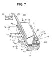
- the recording electrodes E 1 to E n are provided on the upper surface of a glass support 10 at intervals of 125 micrometers in the form of grooves 20 each having a depth of 20 micrometers and a width of 50 micrometers (the spacing between adjacent electrodes being 75 micrometers).
- the electrodes E 1 ⁇ E n and auxiliary electrodes Ao and Ao' are made by vacuum deposition of chromium to the inner walls of the grooves to a thickness of 0.2 micrometers followed by deposition of gold to a thickness of 2 micrometers so that the overlying layer provides a mirror finish surface.
- the spacing between electrodes E 1 and Ao and the spacing between electrodes E n and Ao' are 75 micrometers each.
- the porous member 40 comprises a microporous membrane filter having a thickness of 40 to 200 micrometers and an average pore diameter of 0.1 to 8 micrometers.
- the porous member 40 is in direct contact with the upper surface of the dielectric support 10, the front edge of the porous member being spaced a distance of 50 to 200 micrometers from the front side 12 of the support 10 to expose a portion 30 of the upper surface of support 10 adjacent to its front side.
- a sealing member 60 is used to fill in the grooved electrodes to prevent backflow of ink.
- the front- to-rear edge dimension of the porous member 40 is typically 20 millimeters or greater.
- the overlying mesh electrode 50 has a mesh of 100 to 200 having a thickness of 50 to 100 micrometers to permit inkto permeate therethrough to the underlying porous member 40.
- the ink is supplied to the mesh electrode by means of a sponge conduit 400 from a container 300.
- Fig. 7 even-numbered electrodes are shown biased to the positive turn-off voltage V B during a given half period of a print line interval with respect to the grounded overlying mesh electrode 50 to generate an upward electroosmotic ink movement from such electrodes, causing the ink therein to move toward the rear side of the support 10.
- odd-numbered electrodes are biased to different potentials of negative polarity to cause ink to flow to the front side of the support 10.
- the forward flow of ink is further promoted by electroosmotic action that occurs between adjacent surfaces of the support 10 and the porous member 40.
- the ink is pulled in opposite directions toward the enabled odd-number electrodes as indicated by arrows 207 and collected in such electrodes to produce a flow of ink on the exposed surface 30 that converges to the front end of each enabled electrode.
- the odd-numbered electrodes are then disabled and the even-numbered electrodes are biased to turn-on voltages of different values as mentioned previously.
- the converging effect just described and the alternate enablement of the recording electrodes advantageously coact with each other in eliminating the interference which might otherwise occur between adjacent electrodes, and therefore a sharply defined image is obtained.
- subtle differences, in shading nuance of the original half-tone image can be faithfully reproduced.
- the periodic enablement of the recording electrodes has the effect of averaging out the required power over time, resulting in a reliable printer operation.
- the oppositely moving ink flow constantly flushes the forward end portions of the recording electrodes, where the drying-up of ink would otherwise produce a residual which tends to clog the ink-flow passage, and produces a kind of wiping action clearing any residual substance which might be left in the inkflow passage as a result of drying.
- the annoying clogging problem is automatically eliminated.
- the recording electrodes E, to E n may be divided into three groups with the electrodes of each group being arranged alternately with those of another and that a single print line interval is also divided into equal three periods. In that instance, the electrodes E,, E 4 , E 7 ... are enabled during the first period of each print line interval, the electrodes E 2 , E 5 , E s ... are enabled during the second period of that interval and then the electrodes E 3 , E 6 , Eg... are enabled during the third period.
- the recording paper is advanced at a speed sufficient to allow the ink to separate completely from the recording paper. However, if the paper is advanced at higher speeds, the ink tends to trail as it separates from the paper and interferes with adjacent electrodes causing smearing on the writing surface.
- Fig. 8 is an illustration of an embodiment which eliminates the above-noted problem.
- the individual circuits of the modulator unit 3b are divided into a plurality of blocks of five circuits each and coupled to a switching circuit 4a which in turn comprises a plurality of blocks of five switching elements Sxy each arranged in a pattern of rows and columns represented by subscripts x and y to the letter S.
- Recording electrodes E, to E n are similarly divided into a plurality of blocks corresponding to the modulator unit 3b. All the switching elements S xy are normally coupled to the voltage source 6 to bias the electrodes E, to E n to the turn-off potential V e .
- the switching elements S x1 of each block are arranged in the'#1 column designated 41 and associated with the #1 modulator circuit of each block to couple them simultaneously to the corresponding recording electrodes in response to an output signal on lead 51 of a ring counter RG 1 .
- switching elements S 11 , S 61 ... S (n-4) 1 operate to disconnect the turn-off voltage and connect the individual signals of the modulator circuits #1, #6... #(n-4) to the electrodes E 1 , E 6 ... E n - 4 when an output signal appears on the lead 51.
- the switching elements S x2 of each block are arranged in the #2 column designated 42 and associated with the #3 modulator circuit of each block to couple them simultaneously to the corresponding electrodes in response to an output signal on lead 52 of the ring counter.
- switching elements S 32 , S 82 ... S (n-2) 2 operate to disconnect the turn-off voltage and connect the individual signals of the modulator circuits #3, #8 ... #(n-2) to the electrodes E 3 , E s ... E n - 2 when an output signal appears on the lead 52.
- the switching elements S x3 of each block are arranged in the #3 column designated 43 and associated with the #5 modulator circuit of each block to couple them simultaneously to the corresponding recording electrodes in response to an output signal on lead 53 of the ring counter.
- the switching element S x4 of each block are arranged in the #4 column 44 and associated with the #2 modulator circuit of each block to couple them simultaneously to the corresponding recording electrodes in response to an output signal on lead 54 of the ring counter.
- the switching elements S x5 of each block are arranged in the #5 column 45 and associated with the #4 modulator circuit of each block to couple them to the corresponding recording electrodes in response to an output signal on lead 55 of the ring counter.
- the ring counter RG 1 takes its input from the frequency divider 5c to recyclically apply its output pulse to the output leads 51 to 55 in the order named so that the switching elements are operated successively in the order of the column number. As a result, no adjacent electrodes are successively enabled.
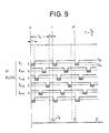
- Fig. 9 shows voltage waveforms applied to the electrodes E,, E r+1 , E r+2 , E r+3 and E r+4 of the #r block.
- the print line interval T comprises a line shift period Tp and an interval To equally divided into five time slots t.
- electrode E r is enabled and driven to a voltage which is shown corresponding to the maximum turn-on voltage Vm for the sake of brevity.
- electrodes E r+2 f E r+4 , E r+1 and E r+3 are enabled in succession in the order named.
- each enablement occurs at such electrodes which are sufficiently spaced from the influence of the "trailing edge" effect of the previously enabled electrodes which would interfere with adjacent electrodes when the printer of the invention is operated at high speeds. It is therefore appropriate for high speed printing that the print line interval is divided by at least five time slots and the minimum number of modulator circuits and recording electrodes within each block is likewise five. In applications where a single pixel is represented by multiple dots, a set of five electrodes can be advantageously assigned to each pixel.
- a line shift pulse tp is generated within the interval Tp but delayed by an appropriate period from the termination of the #5 time slot to allow the trailing edge effect of the electrode E r+3 to decay completely before the print line is shifted to the next.
- Still higher printing speed may be achieved by curtailing the trailing edge effect using a higher turn-off voltage.
- the turn-off time is much longer than the turn-on time for a given electrode, the increase in turn-off voltage would result in a shortage of ink at the instant the given electrode is subsequently enabled.
- Fig. 10 is an illustration of an embodiment which is suitable for such higher printing operations.
- the print line interval is divided into six time slots for purposes of illustration.
- the embodiment of Fig. 10 comprises a plurality of pulse generators PG 1 to PG n corresponding to the recording electrodes E 1 to E n , respectively.
- the pulse generators PG are coupled to receive a triggering signal from a ring counter RG 2 which is in turn coupled to the frequency divider 5c.
- each pulse generator is designed to generate a set of a preceding negative-going pulse n having a duration Ta and a subsequent positive-going pulse p having a duration Tb in response to the recyclically generated triggering signal.
- the interval between the leading edge transitions of such pulses is one-sixth of the print interval To.
- the pulse height of the preceding and succeeding pulses is individually determined in a manner as will be explained later.
- the outputs of the pulse generators PG, to PG n are applied to adders AD, to AD n to be summed with the outputs of the modulator circuits MD 1 to MD n , respectively.
- the outputs of the adders AD 1 to AD n are applied to the switching circuit 4a and thence to the recording electrodes E, to E n .
- This switching circuit is generally similar to that shown in Fig. 8 with the exception that its switching elements are divided into six blocks instead of five.
- the recording electrodes are also divided into six blocks.
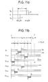
- Fig. 11 b illustrates the waveforms of the combined outputs of the adders AD 1 to AD n to be applied tm a block of six recording electrodes E r to E r+5 .
- the combined output has a negative peak N at the leading edge of the modulated recording pulse extending below the maximum negative level V m and a positive peak P atthe trailing edge which is higher than the turn-off voltage V B .
- the positive peak P serves to reduce the turn-off time by forcibly withdrawing the ink in a short period of time.
- the turn-off voltage V B is chosen so that it causes only a small amount of ink to recede, while the amplitude of the transient turn-off pulse P and its duration are determined so that the combined energy is sufficient to produce quick withdrawal of ink at the termination of each time slot. That application of a negative peak N is effective in reducing the time taken for the ink to move forward.
- the amplitude and duration of this negative pulse are determined so that it produces no ink trace on the writing surface when the recording signal is at the turn-off level. With this embodiment, a printing speed of as high as 10 milliseconds per line was achieved.
- the number of recording electrodes required may be greater than 1700. This requires the corresponding number of driving amplifiers and connecting wires and results in an increase in cost.
- Fig. 12 is an illustration of an electroosmotic ink printer head suitable for high image density applications.
- This printer head is generally similar to that shown in Fig. 1, but differs in that the overlying, mesh electrode 50 is formed by a plurality of segments 50-1 to 50-k.
- a switching circuit used in conjunction with the printer head of Fig. 12.
- the switching circuit comprises a plurality of memories represented by a first group of odd-numbered charge-coupled devices CCD o1 to CCD 08 and a second group of even-numbered charge-coupled devices CCD e1 to CCD e8'
- Each of the odd-numbered charge-coupled devices comprises thirty-two storage locations which are associated with corresponding odd-numbered modulator circuits.
- the even-numbered charge-coupled devices comprises thirty-two storage locations associated with corresponding even-numbered modulator circuits.
- the charge-coupled device CCD 01 has its storage locations coupled to the #1, #3 ...
- #63 modulator circuits and the charge-coupled device CCD os has its storage locations coupled to the #449 to #511 modulator circuits, while CCD e1 is associated with the #2 to #64 modulator circuits and CCD es is associated with the #450 to #512 modulator circuits.
- a ring counter RG 3 is provided to alternately enable the odd- and even-numbered charge-coupled devices and advance the enabling from a lesser to a higher numbered device in response to an output from the frequency divider 5c.
- the odd-numbered charge-coupled devices have their corresponding output terminals multipled for connection to odd-numbered inter-connecting terminals #1 to #63 and the even-numbered charge-coupled devices have their corresponding output terminals multipled for connection to even-numbered inter-connecting terminals #2 to #64.
- the odd-numbered recording electrodes are divided into eight blocks of thirty-two each.
- the first odd-numbered block has its electrodes multipled to the corresponding electrodes of the other odd-numbered blocks for connection to the #1 to #63 odd-numbered inter-connecting terminals.
- electrodes E 1' E 65 , E 129 ... E 449 are coupled together to the #1 inter-connecting terminal.
- the even-numbered recording electrodes are divided into eight blocks of thirty-two each, and these blocks have their corresponding electrodes multipled for connection to the #2 to #64 even-numbered inter-connecting terminals.
- An array of eight mesh electrodes 101 to 108 is provided, each being in overlying relationship with the recording electrodes of a corresponding pair of odd- and even-numbered blocks.
- the mesh electrode 101 overlies the recording electrodes E 1 , E 2 ... E 63 , and E 64 .
- each of the charge-coupled devices transfers the stored dot signals simultaneously to the associated inter-connecting terminals. Therefore, it is seen that the odd- and even-numbered electrodes that underlie each mesh electrode are alternately enabled.
- the mesh electrodes 101 to 108 are biased by enabling voltages supplied from a circuit shown in Fig. 13c.
- This circuit comprises a plurality of analog switches SW 1 to SW 8 which which a turn-on voltage is supplied to a selected mesh electrode from an enabling voltage source VE 1 .
- the analog switches SW 1 to SW 8 are controlled in succession by an output pulse recyclically supplied from a ring counter RG 3 which is responsive to an output of the frequency divider 5c.
- Figs. 15 and 16 The operation of the switching circuit of Figs. 13a to 13c is visualized with reference to waveforms shown in Figs. 15 and 16.
- the numerals shown at left indicate the recording electrodes which are coupled to the corresponding inter-connecting terminals #1 to #64.
- these waveforms will be described, for the time being, as having a rectangular pulse lasting for the full length of the enabled period.
- the print line interval T is divided into eight equal time slots and each time slot is further subdivided into first and second half periods T 1 and T 2 .
- the odd-numbered electrodes E 1 to E 63 are enabled simultaneously during the first half period T 1 of the first time slot and the even-numbered electrodes E 2 to E 64 are enabled simultaneously during the second time slot of the same time slot.
- the mesh electrode 101 which overlies the electrodes E 1 to E 64 , is enabled by a pulse 101-1.
- the odd-numbered electrodes E 65 to E 127 are simultaneously enabled and during the second half period of the same time slot the even-numbered electrodes E 66 to E 128 are simultaneously enabled.
- the second mesh electrode 102 is enabled during this second time slot by a pulse 102-2. This process will be repeated until the recording electrodes E 450 to E 512 are enabled simultaneously with the mesh electrode 108 during the eighth time slot.
- Fig. 16 illustrates the time and amplitude relationships between two pulse signals applied respectively to a given recording electrode and the associated mesh electrode.
- the broken-line waveform is the signal applied to the recording electrode and shown as having an amplitude V AO with a duration Tw and the solid-line waveform indicates the signal applied to the associated mesh electrode.
- the latter signal is shown as having an amplitude V co . If these signals have the amplitude relationships given by then the given recording electrode is driven negative sufficiently with respect to the associated mesh electrode to produce a dot.
- Voltages designated V B ', V B " and V B "' are differences between these pulse signals and appropriately chosen to drive the recording electrode positive sufficiently with respect to the mesh electrode to disable that recording electrode.
- the mesh electrodes 101 to 108 be spaced apart a distance D which is greater than the distance d between the outer edges of two adjacent recording electrodes.
- the mesh electrodes 101 and 102 are spaced apart a distance greater than the distance between the outer edges of the recording electrodes E 63 and E 64 .
- the electrode E 63 when enabled with respect to the electrode 101, acts as a shield between electrodes 101 and E 64 .
- the electrode E 64 when enabled with respect to electrode 102, now acts as a shield between electrodes 102 and E 63 .
- Such shielding effects effectively prevent electromagnetic cross-coupling between undesired electrodes.
- each mesh electrode is associated with a block of an even number of recording electrodes
- the alternate enablement of odd- and even-numbered recording electrodes just described results in a simultaneous enablement of the last one of a preceding block and the first one of a succeeding block.
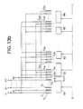
- Figs. 17a-17b are illustrations of a head control circuit adapted for use with the printer head of Fig. 12 in which an odd-number of recording electrodes is associated with each mesh electrode.
- the printer head is shown comprising mesh electrodes ME 1 to ME k and a block of five recording electrodes is associated with each mesh electrode.
- the #1 to #n modulator circuits are connected to a plurality of five-stage charge-coupled devices CCD 1 to CCD k .
- a ring counter RG 5 has its outputs coupled to the charge-coupled devices CCD 1 to CCD k to drive them in sequence in response to an output of the frequency divider 5c so that each charge-coupled device provides a dot-sequential output signal.
- the charge-coupled devices have their corresponding output terminals multipled for connection to the recording electrodes E 1 to E n (Fig. 17b) which are multipled in a manner similar to that of the charge-coupled devices of Fig. 17a.
- the mesh electrodes ME 1 to ME k are coupled through an array of switches SW 1 to SW k to an enabling voltage source VE 2 in response to an output of a ring counter RG 6 which is triggered by the frequency divider 5c as in the previous emebodiments.
- each of the charge-coupled devices CCD 1 to CCD k may be sequentially triggered. However, it is preferable that they be triggered in a manner similar to that shown in Fig. 9.
- Fig. 18 is an illustration of a timing diagram of voltages for enabling the recording electrodes in a manner similar to that shown in Fig. 9 and a timing diagram for sequentially enabling the mesh electrodes as in the embodiment of Figs. 13a-13c.
- the amplitude and timing relationships between the voltages applied to the underlying and mesh electrodes are exactly the same as shown in Fig. 16.
- the #1, #3, #5, #2 and #5 storage locations of charge-coupled device CCD 1 are triggered in sequence by the ring counter RG 5 to enable the recording electrodes E, to E 5 . Similar operation continues until the electrodes E n - 4 to E n are sequentially enabled in response to the enablement of electrode ME k .
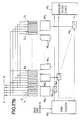
- Figs. 19a-19c are illustrations of a further embodiment of the present invention which eliminates the above-noted cross-coupling problem.
- the arrangement of this embodiment is generally similar to that shown in Figs. 13a-13c to the extent that the recording electrodes E 1 to E 512 are multipled in eight blocks of 64 each.
- charge-coupled devices CCD o1 -CCD o16 and CCD e1 ⁇ CCD e16 are provided to associate with modulator circuits #1 to #512.
- Each of these charge-coupled devices has 16 storage positions.
- the corresponding storage positions of CCD o1' CCD o3 , CCD o5' CCD o7 , CCD o9 , CCD o11 , CCD o13 and CCD o15 are multipled for connection via inter-connecting terminals #1, #3 ...
- each block of 64 recording electrodes is subdivided into a first subgroup of 16 odd-numbered electrodes E 1 , E 3 ... E 31 , a first subgroup of even-numbered 16 electrodes E 2 , E 4 ... E 32 , a second subgroup of 16 odd-numbered electrodes E 33 , E 35 ... E 63 , and a second subgroup of even-numbered electrodes E 34 , E 36 ... E 64 .
- the corresponding electrodes of each subgroup are multipled for connection to the corresponding interconnecting terminals #1 to #64.
- Mesh electrodes ME 1 to ME 17 are provided which are twice as many as there are in the embodiment of Figs. 13a-13c plus one mesh electrode.
- the mesh electrodes ME 1 to ME 17 are arranged so that each mesh electrode is partially associated with preceding subgroups of recording electrodes and partially with adjacent subgroups.
- the mesh electrode ME 2 is associated partially with subgroups E 1 -E 31 and E 2 -E 32 and partially with adjacent subgroups E 33- E 63 and E 34 -E 64 .
- the first and last mesh electrodes ME 1 and ME 17 are each associated with only part of the first and second subgroups.
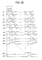
- the print line interval T comprises four time slots t 1 to t 4 and the mesh electrodes are each enabled such that each mesh electrode (except for the first and last mesh electrodes ME 1 and ME 17 ) is impressed with a pulse having a duration Twhich partially overlaps the preceding and succeeding pulses applied to adjacent mesh electrodes.
- the mesh electrodes ME 1 to ME 17 are each impressed with a pulse having half the duration in which the other mesh electrodes are enabled.
- the charge-coupled devices CCD o , and CCD e1 are successively triggered during time slots t 1 and t 2 .
- the odd-numbered recording electrodes E 1 to E 31 are first enabled followed by the enablement of the even-numbered electrodes E 2 to E 32 .
- the odd-numbered electrodes E 33 to E 63 are enabled during time slot t 3 and the even-numbered electrodes E 34 to E 64 are enabled during time slot t 4 . Due to the partial association of the mesh electrodes with the subgroups of recording electrodes and due to the partial overlapped enablement of the mesh electrodes, potential difference no longer occurs between recording and mesh electrodes when the enablement shifts from one multipled group to another.
- the application of potentials could be reversed so that the recording signals are applied to mesh electrodes and the selecting potentials are applied to the recording electrodes. It is also obvious that the present invention could be applied to any type of electroosmotic ink printer, for instance that shown and described in the aforesaid copending application.
Landscapes
- Printers Or Recording Devices Using Electromagnetic And Radiation Means (AREA)
Description
- The present invention relates to an electroosmotic ink printer, and particularly to a method for operating an electroosmotic ink printer head and an electroosmotic ink printer embodying the method.
- Proposals have been made for an electroosmotic ink printer for high printing speed operations, for example European Published
Application 0 048 460, (T Kohashi) (this application falls within the terms ofArticle 54,paragraph 3 of the EPC) which discloses a printer head suitable for use with the present invention. - A typical example of the disclosed printer head comprises a dielectric support, an array of recording electrodes successively arranged on the support and a porous member disposed on the electrode array in contact with the dielectric support. On the porous member is a mesh electrode on which is disposed a means for supplying ink so that it permeates through the mesh electrode down to the porous member. The porous member has its front edge offset from the front side of the head to which a recording sheet is provided, leaving a portion of the recording electrodes and a portion of the dielectric support to be exposed to the outside. This arrangement provides a beneficial effect on the ink by causing it converge into the forward ends of the recording electrodes.
- A circuit is also disclosed which controls the application of modulated potentials simultaneously to the recording electrodes with respect to the overlying mesh electrode. Because of this simultaneous application of potentials, the potential difference between adjacent electrodes is not sufficient under certain circumstances to utilize the converging effect of the ink. This might cause ink dots to spread laterally to adjacent dot positions with the result that the reproduced image is blurred. Additionally, the simultaneous application of potentials tends to produce an excessive amount of ink near the print line position. If a turn-off, or disabling voltage is applied to a certain recording electrode following the printing of such excessive ink, a substantial amount of ink must be withdrawn from the print line position. However, part of the ink would inevitably be left, resulting in a smearing of images. Conversely, if a given electrode is disabled successively by continued application of turn-off voltage, a shortage of ink is likely to occur when that electrode is subsequently enabled for printing.
- One approach to these shortcomings would be to permanently apply a turn-off voltage to alternate ones of the recording electrodes. However, this is only achieved at the cost of reduction in image resolution. A second approach would be to provide a plurality of additional electrodes one on each side of the recording electrodes and apply a turn-off voltage to these additional electrodes. However, the increase in total number of electrodes present difficulties in manufacture and in operation since the additional electrodes would also cause retraction of an excessive ink which in turn requires a high voltage to move it forward.
- It is therefore an object of the present invention to provide a method for operating an electroosmotic ink printer head to ensure against smearing of images and allow the printer head to successfully operate at high printing speeds and to provide an electroosmotic ink printer embodying the method.
- The electroosmotic ink printer head adapted for use in the invention comprises an array of recording electrodes successively arranged to define a print line along one edge of the head, an overlying electrode means in spaced overlying relationship with the recording electrodes and means provided between the electrode array and the overlying electrode means for electroosmotically moving ink in a direction towards the print line or in an opposite direction depending on an electrical potential applied to the recording electrodes with respect to the overlying electrode means.
- According to the present invention, there is provided a method of operating an electroosmotic ink printer head including an array of recording electrodes successively arranged to define a print line along one edge of said head, an overlying electrode means in spaced overlying relationship with the recording electrodes and means provided between said electrode array and said overlying electrode means for electroosmotically moving ink in a direction towards said print line or in an opposite direction depending on an electrical potential applied to said recording electrodes with respect to the overlying electrode means, characterised by the steps of:
- a) storing an input signal in a plurality of storage locations corresponding to said recording electrodes; and
- b) disabling a first group of said recording electrodes by applying thereto a first potential to cause said ink to move in the opposite direction while enabling a second group of said recording electrodes by applying thereto a second potential to cause said ink to move to said print line and subsequently disabling said second group while enabling said first group, the electrodes of each group being located alternately with those of the other.
- The alternating disablement of the electrodes keeps them from being affected adversely by the electric field generated in adjacent electrodes. The input signal can be a video signal, i.e. a signal for reproducing a television picture, but could take other forms.
- Preferably, the recording electrodes are organised into a plurality of blocks each having at least five such recording electrodes, and the electrodes of each block are further organised with the corresponding electrodes of the other blocks to form at least five groups. The second, or disabling potential is applied to the electrodes of each block in such a sequence that the successively applied electrodes are spaced a distance greater than the distance at which the recording electrodes are spaced apart. This ensures against undesirable interference which may arise between adjacent electrodes when activated in succession.
- According to a second aspect the present invention provides a printer adapted to receive an input signal for printing an image, wherein the printer includes an electroosmotic ink printer head having an array of recording electrodes successively arranged to define a print line along one edge of said head, an overlying electrode means in spaced overlying relationship with the recording electrodes and means provided between said electrode array and said overlying electrode means for electroosmotically moving ink in a direction toward said print line or in an opposite direction depending on an electrical potential applied to said recording electrodes with respect to the overlying electrode means, characterised by:
- memory means for storing said input signal in a plurality of storage locations corresponding to said recording electrodes;
- modulating means for modulating a first electrical potential with the signals stored in said storage locations to generate individual recording signals corresponding to said recording electrodes, said first potential having a polarity which causes the ink to move to the print line;
- timing means for generating a timing signal to define a periodic interval during which said image is to be printed on said print line, said interval being divided into at least first and second time slots;
- means for organising said recording electrodes into first and second groups, the electrodes of each group being located adjacent to the corresponding electrodes of the other group; and
- control means for activating a portion of said recording electrodes by sequentially applying said individual recording signals to said first and second groups during said first and second time slots respectively to cause the ink on the activated electrodes to move to the print line to form said image on a surface, and for deactivating the remainder of said recording electrodes by applying a second electrical potential to the electrodes of the group to which said recording signals are not applied, said second potential having a polarity which causes the ink to move in the opposite direction.
- The invention will be more clearly understood from the following description which is given by way of example only, with reference to the accompanying drawings, in which:-
- Fig. 1 is an illustration of a block diagram of a first embodiment of the present invention in which the recording electrodes are alternately disabled;
- Fig. 2 is a block diagram illustrating an alternative form of the Fig. 1 embodiment;
- Fig. 3 is a diagram illustrating the waveforms of recording signals which are modulated discretely in amplitude between disabling and enabling levels with a digital video signal and applied to adjacent ones of the recording electrodes for describing an operation of the Fig. 1 embodiment;
- Fig. 4 is a sketch illustrating an image produced according the timing diagram of Fig. 3;
- Fig. 5 is a diagram illustrating the waveforms of recording signals which are modulated continuously in amplitude between disabling and enabling levels with an analog video signal and applied to adjacent ones of the recording electrodes for describing another manner of operation of the Fig. 1 embodiment;
- Fig. 6 is a diagram illustrating the waveforms of recording signals which are modulated in pulse width according to an input video signal and applied to adjacent electrodes for describing another manner of operation of the Fig. 1 embodiment;
- Fig. 7 is a perspective view of a typical example of electroosmotic ink printer heads which are adapted for use in the present invention;
- Fig. 8 is an illustration of a second embodiment of the present invention, showing the detail of the switching circuit of Fig. 1;
- Fig. 9 is a timing diagram associated with the embodiment of Fig. 8;
- Fig. 10 is an illustration of a modified form of the second embodiment;
- Figs. 11 a and 11 b are illustrations of waveform and timing diagrams, respectively, of the signals appearing in the embodiment of Fig. 10;
- Fig. 12 is a perspective view of an electroosmotic ink printer head having a plurality of overlying segmented electrodes adapted for use in a third embodiment of the invention;
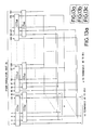
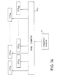
- Figs. 13a-13c and 14 are block diagrams of the third embodiment in which an even number of recording electrodes is multipled to form a plurality of blocks;
- Fig. 15 is a timing diagram useful for describing the operation of the third embodiment;
- Fig. 16 is a diagram associated with the third embodiment illustrating waveforms applied respectively to a given recording electrode and an associated overlying segmented electrode;
- Figs. 17a-17b are block diagrams illustrating a modified form of the third embodiment;
- Fig. 18 is a timing diagram associated with the block diagram of Figs. 17a-17b;
- Figs. 19a-19c are illustrations of a further modified form of the third embodiment of the invention; and
- Fig. 20 is a timing diagram for describing the operation of the embodiment of Figs. 19a-19c.
- Referring now to Fig. 1, the electroosmotic ink printer of the invention is schematically illustrated. Illustrated at 100 is an electroosmotic ink printer head having an array of first, elongated recording electrodes E1, E2, E3 ... En successively arranged on the surface of a
dielectric support 10 each extending across the front andrear sides 12 and 13 of thesupport 10. On the electrode array is aporous member 40 of dielectric material on which is provided a second,mesh electrode 50 which, in the illustrated embodiment, is connected to a ground terminal. As will be shown later, an ink supply means is provided on themesh electrode 50. A sheet ofrecording paper 500 is in pressure contact with thefront side 12 of thesupport 10 by engagement with aplaten 600 to form a print line by a multitude of ink protuberances produced in a manner as will be described later at the front ends of the recording electrodes E. The supplied ink permeates through themesh electrode 50 down to theporous member 40. Under the influence of potentials applied to the first and second electrodes the permeating ink is caused to electroosmotically migrate to those of the recording electrodes which are biased negative with respect to theoverlying mesh electrode 50 and collect at the front ends of such electrodes. - Since the ink has a tendency to spontaneously exude from the
porous member 40 and flood the corner areas of the support including the area which contacts with the recording sheet, it is preferable that the opposite end portions of the support's upper surface be covered by auxiliary electrodes Ao and Ao' that extends between thefront side 12 and the rear side 13 in spaced parallel relationship with the outermost electrodes E1 and En (the spacing being substantially equal to the spacing between adjacent ones of the first electrodes). - A dot-sequential video input signal is applied to a
line memory 2. The type of video input signal may be in the form of the standard composite television signal or a facsimile signal. Theline memory 2 is of an analog type memory such as charge-coupled devices to convert the dot-sequential signal to a line-sequential signal by storing the video input signal into successive dot storage positions and simultaneously transmitting the dot-position signals to ahead drive circuit 3. Thedrive circuit 3 comprises an analogdigital converter unit 3a and amodulator unit 3b. The types of modulation suitable for the present invention include pulse-width modulation, amplitude modulation, and pulse-width amplitude modulation. Alternatively, the input video signal is converted to a digital signal by theconverter unit 3a and then stored into a digital memory such as random access memory or a shift register as shown in Fig. 2. - The video input signal is also applied to a
timing pulse generator 5 which comprises async separator 5a for detecting the horizontal synchronization pulse, a phase-locked loop oscillator 5b responsive to the horizontal sync supplied from theseparater 5a. The signal from the oscillator 5b is applied to afrequency divider 5c. Thefrequency divider 5c provides various timing pulses to other parts of the system. The A/D converter unit 3a is an LSI circuit which includes a plurality of A/D converters arranged in correspondance with the dot positions. The dot-position signals are converted to digital signals which are applied to the modulator unit for modulating a predetermined DC voltage to generate negative voltages of different amplitudes. For this reason, themodulator unit 3b also comprises an LSI circuit including a plurality of modulator circuits corresponding in number to the A/D converter circuits. In one application the modulator circuits are of a well known amplitude-modulation type which modulates the amplitude of the DC voltage in accordance with the modulating digital signals. In another application, the modulator circuits are of a known pulse-width modulation type which generates a pulse of a preselected amplitude having a width variable as a function of the modulating digital signals. Theline memory 2,AID converter unit 3a andmodulator unit 3b are all operated in unison in response to the respective timing signals supplied from thefrequency divider 5c. - The modulated video signals are applied to a
switching circuit 4 having a plurality of electronic switching elements S1 to Sn with the moving contact arms being connected to the recording electrodes E1 to E", respectively. Each switching element has stationary terminals designated a and b with the terminal a being coupled to the outputs of the corresponding modulator circuits and the terminal b being coupled together to acommon voltage source 6 having a positive turn-off voltage Ve. The odd-numbered switching elements are shown connected to the outputs of the modulator circuits, while the even-numbered switching elements are connected to the turn-offvoltage source 6. This switching circuit is controlled by a timing signal supplied from thefrequency divider 5c to alternately apply the turn-off and turn-on (recording signal) voltages to the associated recording electrodes. Thefrequency divider 5c also provides a paper advance control signal immediately following the termination of each print line to apulse motor 7 which drives theplaten 600 to successively advance thepaper 500 by the width of a print line. - For the purpose of explanation it is assumed that the modulator circuits are of the amplitude modulation type.
- The switching control signal is generated for each line-sequential signal so that during a first half period of each print-line interval odd-numbered recording electrodes are biased to the turn-off potential VB and even-numbered electrodes are biased individually to the potentials of the amplitude-modulated signals and during a second half period of that interval the switching elements are all transferred to apply the turn-off voltage to the even-numbered electrodes and apply the modulated potentials to the odd-numbered electrodes. Therefore, when a given electrode is applied with a modulated negative
potential mesh electrode 50 or "enabled" for printing, adjacent electrodes are applied with the positive turn-off voltage or "disabled". - The auxiliary electrodes Ao and Ao' are biased to a voltage VA from a
source 8 which is positive with respect to themesh electrode 50 to cause the ink contained in theporous member 40 to electroosmotically move in a direction from the auxiliary electrodes Ao, Ao' to themesh electrode 50, whereby the ink flooding the corner areas of thesupport 10 recedes from the front edge. The voltages VA and VB are selected to be of the same value. - In one application, the recording electrodes are provided in such a number that each pixel on the recording surface is formed by plural dots of one of high and low discrete tone values. In such applications, the potential of the amplitude-modulated signal is varied between the turn-off voltage VB and a negative turn-on voltage of a maximum value which is referred to as voltage Vm.
- Fig. 3 is an illustration of waveforms of the discretely modulated signals applied to adjacent electrodes represented by Er and Er+1 (where, r is an arbitrary number between 1 and n-1) during the interval of three print lines for the purpose of explanation. Hatching is used to indicate the interval of enabled period and the tone value, with the single-hatch indicating the signal driven in a direction toward increasing the tone value and the cross-hatch indicating the signal driven in a direction toward decreasing the tone value.
- During the first half period of the #1 print line interval T, the electrode Er is in the enabled state and is assumed to be biased to a turn-on voltage of maximum value Vm, while the electrode Er+1 is biased to the turn-off voltage VB to be disabled. During the second half period of the #1 print line interval, the electrode Er is disabled and the electrode Er+1 is biased to a voltage modulated to the maximum turn-on level Vm. Therefore, black squares d11 and d12 are produced by electrodes Er and Er+1 on the #1 print line as shown in Fig. 4.
- During the first half period of the second time print line interval, electrodes Er and Er+1 are enabled and disabled respectively. The potential to be applied to the enabled electrode Er is assumed to be modulated to the turn-off level VB as indicated by a cross-hatched area so that this electrode produces a blank in the #2 print line, while the electrode Er+1 is forced to the turn-off level VB. During the second half period of the #2 print line interval, electrodes Er and Er+1 are switched to the disabled and enabled states respectively. The potential applied to electrode Er+1 is assumed to be modulated to the negative maximum turn-on voltage Vm producing a black square d22 on the #2 print line.
- Similarly, during the first half period of the #3 print line interval, electrode Er is enabled and driven to the negative maximum voltage and electrode Er+1 is disabled, producing a black square d13 on the #3 print line and during the second half period, the enabled electrode Er+1 is driven to a voltage which is assumed to be modulated to the turn-off level VB, thus leading a blank in the #3 print line adjacent to black area d13.
- Fig. 5 is an illustration of a waveform diagram associated with amplitude modulation which is used in applications wherein each pixel is formed by a single dot or square of half-tone value which is a function of the amplitude modulation. The potentials to be applied to the enabled electrodes are modulated continuously in amplitude between the positive turn-off level VB and the maximum negative turn-on level Vm. A modulated potential having the maximum turn-on level Vm is shown applied to electrode Er during the first half period of the #1 print line interval. This produces a dot of the largest size on the #1 print line. Amplitude modulation of a lesser degree may produce a lower turn-on voltage which, when applied to electrode E2 during the second half period will produce a dot of a size slightly smaller than the largest size. The half tone value is determined by the degree of amplitude modulation and thus varies as a function of voltage deviation from the turn-off level VB. Thus, a half-tone value which is close to the blank level can thus be produced by application of a positive voltage close to the turn-off level VB as indicated by V2.
- For half-tone image reproduction, the amount of energy supplied to the enabled electrodes is not only variable in terms of voltage, but also variable in terms of pulse duration. Pulse-width modulation can thus be employed in the present invention. In this instance, the enabled electrodes are first driven negatively to the same maximum turn-on voltage Vm but for different durations as a function of the desired half-tone value and then positively driven to the turn-off level VB during the rest of the enabled period.
- Pulse-width modulator circuits are included in the
modulator unit 3b to effect such pulse-width modulation on each dot signal. Each of the pulse-width modulators is responsive to the digital modulating signal by generating a pulse of negative voltage Vm having a variable duration corresponding to the desired half-tone density and a pulse of positive turn-off voltage VB having a duration complementary to the duration of the negative pulse. An example of the waveforms generated by such modulator circuits for electrodes E, and Er+1 is shown in Fig. 6. - Details of the structure and operation of the
printer head 100 are shown in perspective view in Fig. 7. The recording electrodes E1 to En are provided on the upper surface of aglass support 10 at intervals of 125 micrometers in the form ofgrooves 20 each having a depth of 20 micrometers and a width of 50 micrometers (the spacing between adjacent electrodes being 75 micrometers). The electrodes E1―En and auxiliary electrodes Ao and Ao' are made by vacuum deposition of chromium to the inner walls of the grooves to a thickness of 0.2 micrometers followed by deposition of gold to a thickness of 2 micrometers so that the overlying layer provides a mirror finish surface. The spacing between electrodes E1 and Ao and the spacing between electrodes En and Ao' are 75 micrometers each. - The
porous member 40 comprises a microporous membrane filter having a thickness of 40 to 200 micrometers and an average pore diameter of 0.1 to 8 micrometers. Theporous member 40 is in direct contact with the upper surface of thedielectric support 10, the front edge of the porous member being spaced a distance of 50 to 200 micrometers from thefront side 12 of thesupport 10 to expose aportion 30 of the upper surface ofsupport 10 adjacent to its front side. A sealingmember 60 is used to fill in the grooved electrodes to prevent backflow of ink. The front- to-rear edge dimension of theporous member 40 is typically 20 millimeters or greater. Theoverlying mesh electrode 50 has a mesh of 100 to 200 having a thickness of 50 to 100 micrometers to permit inkto permeate therethrough to the underlyingporous member 40. The ink is supplied to the mesh electrode by means of asponge conduit 400 from acontainer 300. - In Fig. 7, even-numbered electrodes are shown biased to the positive turn-off voltage VB during a given half period of a print line interval with respect to the grounded overlying
mesh electrode 50 to generate an upward electroosmotic ink movement from such electrodes, causing the ink therein to move toward the rear side of thesupport 10. At the same time, odd-numbered electrodes are biased to different potentials of negative polarity to cause ink to flow to the front side of thesupport 10. The forward flow of ink is further promoted by electroosmotic action that occurs between adjacent surfaces of thesupport 10 and theporous member 40. On the exposedsurface portion 30 the ink is pulled in opposite directions toward the enabled odd-number electrodes as indicated byarrows 207 and collected in such electrodes to produce a flow of ink on the exposedsurface 30 that converges to the front end of each enabled electrode. During the next half period, the odd-numbered electrodes are then disabled and the even-numbered electrodes are biased to turn-on voltages of different values as mentioned previously. - The converging effect just described and the alternate enablement of the recording electrodes advantageously coact with each other in eliminating the interference which might otherwise occur between adjacent electrodes, and therefore a sharply defined image is obtained. In particular, subtle differences, in shading nuance of the original half-tone image can be faithfully reproduced. The periodic enablement of the recording electrodes has the effect of averaging out the required power over time, resulting in a reliable printer operation. Furthermore, the oppositely moving ink flow constantly flushes the forward end portions of the recording electrodes, where the drying-up of ink would otherwise produce a residual which tends to clog the ink-flow passage, and produces a kind of wiping action clearing any residual substance which might be left in the inkflow passage as a result of drying. Thus, the annoying clogging problem is automatically eliminated.
- The recording electrodes E, to En may be divided into three groups with the electrodes of each group being arranged alternately with those of another and that a single print line interval is also divided into equal three periods. In that instance, the electrodes E,, E4, E7 ... are enabled during the first period of each print line interval, the electrodes E2, E5, Es ... are enabled during the second period of that interval and then the electrodes E3, E6, Eg... are enabled during the third period.
- Due to the inherent viscosity of the ink that causes it to stick to the
paper 500, the recording paper is advanced at a speed sufficient to allow the ink to separate completely from the recording paper. However, if the paper is advanced at higher speeds, the ink tends to trail as it separates from the paper and interferes with adjacent electrodes causing smearing on the writing surface. - Fig. 8 is an illustration of an embodiment which eliminates the above-noted problem. In this embodiment the individual circuits of the
modulator unit 3b are divided into a plurality of blocks of five circuits each and coupled to a switching circuit 4a which in turn comprises a plurality of blocks of five switching elements Sxy each arranged in a pattern of rows and columns represented by subscripts x and y to the letter S. Recording electrodes E, to En are similarly divided into a plurality of blocks corresponding to themodulator unit 3b. All the switching elements Sxy are normally coupled to thevoltage source 6 to bias the electrodes E, to En to the turn-off potential Ve. The switching elements Sx1 of each block are arranged in the'#1 column designated 41 and associated with the #1 modulator circuit of each block to couple them simultaneously to the corresponding recording electrodes in response to an output signal onlead 51 of a ring counter RG1. For example, switching elements S11, S61 ...S (n-4)1 operate to disconnect the turn-off voltage and connect the individual signals of themodulator circuits # 1, #6... #(n-4) to the electrodes E1, E6 ... En-4 when an output signal appears on thelead 51. The switching elements Sx2 of each block are arranged in the #2 column designated 42 and associated with the #3 modulator circuit of each block to couple them simultaneously to the corresponding electrodes in response to an output signal onlead 52 of the ring counter. For example, switching elements S32, S82 ...S (n-2)2 operate to disconnect the turn-off voltage and connect the individual signals of themodulator circuits # 3, #8 ... #(n-2) to the electrodes E3, Es ... En-2 when an output signal appears on thelead 52. Likewise, the switching elements Sx3 of each block are arranged in the #3 column designated 43 and associated with the #5 modulator circuit of each block to couple them simultaneously to the corresponding recording electrodes in response to an output signal onlead 53 of the ring counter. The switching element Sx4 of each block are arranged in the #4 column 44 and associated with the #2 modulator circuit of each block to couple them simultaneously to the corresponding recording electrodes in response to an output signal onlead 54 of the ring counter. Finally, the switching elements Sx5 of each block are arranged in the #5 column 45 and associated with the #4 modulator circuit of each block to couple them to the corresponding recording electrodes in response to an output signal onlead 55 of the ring counter. The ring counter RG1 takes its input from thefrequency divider 5c to recyclically apply its output pulse to the output leads 51 to 55 in the order named so that the switching elements are operated successively in the order of the column number. As a result, no adjacent electrodes are successively enabled. Fig. 9 shows voltage waveforms applied to the electrodes E,, Er+1, Er+2, Er+3 and Er+4 of the #r block. The print line interval T comprises a line shift period Tp and an interval To equally divided into five time slots t. During the first time slot electrode Er is enabled and driven to a voltage which is shown corresponding to the maximum turn-on voltage Vm for the sake of brevity. During thesubsequent # 2 to #5 time slots, electrodes Er+2f Er+4, Er+1 and Er+3 are enabled in succession in the order named. - Therefore, it is seen that each enablement occurs at such electrodes which are sufficiently spaced from the influence of the "trailing edge" effect of the previously enabled electrodes which would interfere with adjacent electrodes when the printer of the invention is operated at high speeds. It is therefore appropriate for high speed printing that the print line interval is divided by at least five time slots and the minimum number of modulator circuits and recording electrodes within each block is likewise five. In applications where a single pixel is represented by multiple dots, a set of five electrodes can be advantageously assigned to each pixel.
- A line shift pulse tp is generated within the interval Tp but delayed by an appropriate period from the termination of the #5 time slot to allow the trailing edge effect of the electrode Er+3 to decay completely before the print line is shifted to the next.
- Still higher printing speed may be achieved by curtailing the trailing edge effect using a higher turn-off voltage. However, since the turn-off time is much longer than the turn-on time for a given electrode, the increase in turn-off voltage would result in a shortage of ink at the instant the given electrode is subsequently enabled.
- Fig. 10 is an illustration of an embodiment which is suitable for such higher printing operations. In this embodiment, the print line interval is divided into six time slots for purposes of illustration.
- The embodiment of Fig. 10 comprises a plurality of pulse generators PG1 to PGn corresponding to the recording electrodes E1 to En, respectively. The pulse generators PG are coupled to receive a triggering signal from a ring counter RG2 which is in turn coupled to the
frequency divider 5c. As shown in Fig. 11 a, each pulse generator is designed to generate a set of a preceding negative-going pulse n having a duration Ta and a subsequent positive-going pulse p having a duration Tb in response to the recyclically generated triggering signal. The interval between the leading edge transitions of such pulses is one-sixth of the print interval To. The pulse height of the preceding and succeeding pulses is individually determined in a manner as will be explained later. - The outputs of the pulse generators PG, to PGn are applied to adders AD, to ADn to be summed with the outputs of the modulator circuits MD1 to MDn, respectively. The outputs of the adders AD1 to ADn are applied to the switching circuit 4a and thence to the recording electrodes E, to En. This switching circuit is generally similar to that shown in Fig. 8 with the exception that its switching elements are divided into six blocks instead of five. The recording electrodes are also divided into six blocks. Fig. 11 b illustrates the waveforms of the combined outputs of the adders AD1 to ADn to be applied tm a block of six recording electrodes Er to Er+5. As illustrated, the combined output has a negative peak N at the leading edge of the modulated recording pulse extending below the maximum negative level Vm and a positive peak P atthe trailing edge which is higher than the turn-off voltage VB. The positive peak P serves to reduce the turn-off time by forcibly withdrawing the ink in a short period of time. The turn-off voltage VB is chosen so that it causes only a small amount of ink to recede, while the amplitude of the transient turn-off pulse P and its duration are determined so that the combined energy is sufficient to produce quick withdrawal of ink at the termination of each time slot. That application of a negative peak N is effective in reducing the time taken for the ink to move forward. The amplitude and duration of this negative pulse are determined so that it produces no ink trace on the writing surface when the recording signal is at the turn-off level. With this embodiment, a printing speed of as high as 10 milliseconds per line was achieved.
- For high image density reproduction the number of recording electrodes required may be greater than 1700. This requires the corresponding number of driving amplifiers and connecting wires and results in an increase in cost.
- Fig. 12 is an illustration of an electroosmotic ink printer head suitable for high image density applications. This printer head is generally similar to that shown in Fig. 1, but differs in that the overlying,
mesh electrode 50 is formed by a plurality of segments 50-1 to 50-k. - In Figs. 13a to 13c and 14 is illustrated a switching circuit used in conjunction with the printer head of Fig. 12. The switching circuit comprises a plurality of memories represented by a first group of odd-numbered charge-coupled devices CCDo1 to CCD08 and a second group of even-numbered charge-coupled devices CCDe1 to CCDe8' Each of the odd-numbered charge-coupled devices comprises thirty-two storage locations which are associated with corresponding odd-numbered modulator circuits. Likewise, the even-numbered charge-coupled devices comprises thirty-two storage locations associated with corresponding even-numbered modulator circuits. For example, the charge-coupled device CCD01 has its storage locations coupled to the #1, #3 ... #63 modulator circuits and the charge-coupled device CCDos has its storage locations coupled to the #449 to #511 modulator circuits, while CCDe1 is associated with the #2 to #64 modulator circuits and CCDes is associated with the #450 to #512 modulator circuits. As shown in Fig. 14, a ring counter RG3 is provided to alternately enable the odd- and even-numbered charge-coupled devices and advance the enabling from a lesser to a higher numbered device in response to an output from the
frequency divider 5c. - The odd-numbered charge-coupled devices have their corresponding output terminals multipled for connection to odd-numbered
inter-connecting terminals # 1 to #63 and the even-numbered charge-coupled devices have their corresponding output terminals multipled for connection to even-numberedinter-connecting terminals # 2 to #64. - As illustrated in Fig. 13b, the odd-numbered recording electrodes are divided into eight blocks of thirty-two each. The first odd-numbered block has its electrodes multipled to the corresponding electrodes of the other odd-numbered blocks for connection to the #1 to #63 odd-numbered inter-connecting terminals. For example, electrodes E1' E65, E129 ... E449 are coupled together to the #1 inter-connecting terminal. Similarly, the even-numbered recording electrodes are divided into eight blocks of thirty-two each, and these blocks have their corresponding electrodes multipled for connection to the #2 to #64 even-numbered inter-connecting terminals. An array of eight
mesh electrodes 101 to 108 is provided, each being in overlying relationship with the recording electrodes of a corresponding pair of odd- and even-numbered blocks. For example, themesh electrode 101 overlies the recording electrodes E1, E2 ... E63, and E64. - When enabled, each of the charge-coupled devices transfers the stored dot signals simultaneously to the associated inter-connecting terminals. Therefore, it is seen that the odd- and even-numbered electrodes that underlie each mesh electrode are alternately enabled.
- The
mesh electrodes 101 to 108 are biased by enabling voltages supplied from a circuit shown in Fig. 13c. This circuit comprises a plurality of analog switches SW1 to SW8 which which a turn-on voltage is supplied to a selected mesh electrode from an enabling voltage source VE1. The analog switches SW1 to SW8 are controlled in succession by an output pulse recyclically supplied from a ring counter RG3 which is responsive to an output of thefrequency divider 5c. - The operation of the switching circuit of Figs. 13a to 13c is visualized with reference to waveforms shown in Figs. 15 and 16. In Fig. 15, the numerals shown at left indicate the recording electrodes which are coupled to the corresponding
inter-connecting terminals # 1 to #64. For the sake of brevity, these waveforms will be described, for the time being, as having a rectangular pulse lasting for the full length of the enabled period. - The print line interval T is divided into eight equal time slots and each time slot is further subdivided into first and second half periods T1 and T2. The odd-numbered electrodes E1 to E63 are enabled simultaneously during the first half period T1 of the first time slot and the even-numbered electrodes E2 to E64 are enabled simultaneously during the second time slot of the same time slot. During this first time slot, the
mesh electrode 101, which overlies the electrodes E1 to E64, is enabled by a pulse 101-1. In like manner, during the first half period of the second time slot the odd-numbered electrodes E65 to E127 are simultaneously enabled and during the second half period of the same time slot the even-numbered electrodes E66 to E128 are simultaneously enabled. At the same time, thesecond mesh electrode 102 is enabled during this second time slot by a pulse 102-2. This process will be repeated until the recording electrodes E450 to E512 are enabled simultaneously with themesh electrode 108 during the eighth time slot. - Fig. 16 illustrates the time and amplitude relationships between two pulse signals applied respectively to a given recording electrode and the associated mesh electrode. The broken-line waveform is the signal applied to the recording electrode and shown as having an amplitude VAO with a duration Tw and the solid-line waveform indicates the signal applied to the associated mesh electrode. The latter signal is shown as having an amplitude Vco. If these signals have the amplitude relationships given by


- It will be seen from the above that the number of connecting wires between the
printer head 100 and the head control circuit are reduced by the factor of eight. Therefore, the number of amplifiers required can be drastically reduced. - Returning to Fig. 13b, it is preferable that the
mesh electrodes 101 to 108 be spaced apart a distance D which is greater than the distance d between the outer edges of two adjacent recording electrodes. For example, themesh electrodes electrode 101, acts as a shield betweenelectrodes 101 and E64. Conversely, the electrode E64, when enabled with respect toelectrode 102, now acts as a shield betweenelectrodes 102 and E63. Such shielding effects effectively prevent electromagnetic cross-coupling between undesired electrodes. - While in the embodiment of Figs. 13a-13c, each mesh electrode is associated with a block of an even number of recording electrodes, it is also possible to form the block with an odd number of recording electrodes. However, the alternate enablement of odd- and even-numbered recording electrodes just described results in a simultaneous enablement of the last one of a preceding block and the first one of a succeeding block.
- Figs. 17a-17b are illustrations of a head control circuit adapted for use with the printer head of Fig. 12 in which an odd-number of recording electrodes is associated with each mesh electrode. For purposes of disclosure the printer head is shown comprising mesh electrodes ME1 to MEk and a block of five recording electrodes is associated with each mesh electrode.
- In Fig. 17a, the #1 to #n modulator circuits are connected to a plurality of five-stage charge-coupled devices CCD1 to CCDk. A ring counter RG5 has its outputs coupled to the charge-coupled devices CCD1 to CCDk to drive them in sequence in response to an output of the
frequency divider 5c so that each charge-coupled device provides a dot-sequential output signal. The charge-coupled devices have their corresponding output terminals multipled for connection to the recording electrodes E1 to En (Fig. 17b) which are multipled in a manner similar to that of the charge-coupled devices of Fig. 17a. - The mesh electrodes ME1 to MEk are coupled through an array of switches SW1 to SWk to an enabling voltage source VE2 in response to an output of a ring counter RG6 which is triggered by the
frequency divider 5c as in the previous emebodiments. - The storage locations of each of the charge-coupled devices CCD1 to CCDk may be sequentially triggered. However, it is preferable that they be triggered in a manner similar to that shown in Fig. 9. Fig. 18 is an illustration of a timing diagram of voltages for enabling the recording electrodes in a manner similar to that shown in Fig. 9 and a timing diagram for sequentially enabling the mesh electrodes as in the embodiment of Figs. 13a-13c. The amplitude and timing relationships between the voltages applied to the underlying and mesh electrodes are exactly the same as shown in Fig. 16.
- In a typical example, when the first mesh electrode ME1 is enabled, the #1, #3, #5, #2 and #5 storage locations of charge-coupled device CCD1 are triggered in sequence by the ring counter RG5 to enable the recording electrodes E, to E5. Similar operation continues until the electrodes En-4 to En are sequentially enabled in response to the enablement of electrode MEk.
- Figs. 19a-19c are illustrations of a further embodiment of the present invention which eliminates the above-noted cross-coupling problem.
- The arrangement of this embodiment is generally similar to that shown in Figs. 13a-13c to the extent that the recording electrodes E1 to E512 are multipled in eight blocks of 64 each. As illustrated in Fig. 19a, charge-coupled devices CCDo1-CCDo16 and CCDe1―CCDe16 are provided to associate with
modulator circuits # 1 to #512. Each of these charge-coupled devices has 16 storage positions. The corresponding storage positions of CCDo1' CCDo3, CCDo5' CCDo7, CCDo9, CCDo11, CCDo13 and CCDo15 are multipled for connection viainter-connecting terminals # 1, #3 ... #31 to recording electrodes E1, E3 ... E31. The corresponding storage positions of CCDe1, CCDe3, CCDe5, CCDe7' CCDe9, CCDe11, CCDe13 and CCDe15 are multipled for connection viainter-connecting terminals # 2, #4... #32 to recording electrodes E2, E4 ... E32. Likewise, the corresponding storage positions of CCDo2, CCDo4, CCDo6' CCDo8' CCDo10, CCDo12' CCDo14 and CCDo16 are multipled for connection viainter-connecting terminals # 33, #35 ... #63 to recording electrodes E33, E35 ... E63, and the corresponding storage positions of CCDe2, CCDe4, CCDe6, CCDe8, CCDe10 CCDe12 CCDe14 and CCDe16 are multipled for connection viainter-connecting terminals # 34, #36 ... #64 to recording electrodes E34, E36 ... E64, - As shown in Fig. 19b, each block of 64 recording electrodes is subdivided into a first subgroup of 16 odd-numbered electrodes E1, E3 ... E31, a first subgroup of even-numbered 16 electrodes E2, E4... E32, a second subgroup of 16 odd-numbered electrodes E33, E35 ... E63, and a second subgroup of even-numbered electrodes E34, E36 ... E64. The corresponding electrodes of each subgroup are multipled for connection to the corresponding
interconnecting terminals # 1 to #64. Mesh electrodes ME1 to ME17 are provided which are twice as many as there are in the embodiment of Figs. 13a-13c plus one mesh electrode. The mesh electrodes ME1 to ME17 are arranged so that each mesh electrode is partially associated with preceding subgroups of recording electrodes and partially with adjacent subgroups. For example, the mesh electrode ME2 is associated partially with subgroups E1-E31 and E2-E32 and partially with adjacent subgroups E33-E63 and E34-E64. On the other hand, the first and last mesh electrodes ME1 and ME17 are each associated with only part of the first and second subgroups. - These charge-coupled devices are controlled sequentially by a ring counter RG7 (Fig. 19c) and the mesh electrodes ME1 to ME17 are enabled by a voltage source VE3 through switches SW, to SW17 under the control of a ring counter RG8. As will be understood from Fig. 20, the print line interval T comprises four time slots t1 to t4 and the mesh electrodes are each enabled such that each mesh electrode (except for the first and last mesh electrodes ME1 and ME17) is impressed with a pulse having a duration Twhich partially overlaps the preceding and succeeding pulses applied to adjacent mesh electrodes. The mesh electrodes ME1 to ME17 are each impressed with a pulse having half the duration in which the other mesh electrodes are enabled. When the mesh electrode ME1 is enabled the charge-coupled devices CCDo, and CCDe1 are successively triggered during time slots t1 and t2. As a result, the odd-numbered recording electrodes E1 to E31 are first enabled followed by the enablement of the even-numbered electrodes E2 to E32. The odd-numbered electrodes E33 to E63 are enabled during time slot t3 and the even-numbered electrodes E34 to E64 are enabled during time slot t4. Due to the partial association of the mesh electrodes with the subgroups of recording electrodes and due to the partial overlapped enablement of the mesh electrodes, potential difference no longer occurs between recording and mesh electrodes when the enablement shifts from one multipled group to another. Specifically, when enablement shifts from electrodes E4to Es the simultaneous presence of the same potential on the mesh electrodes ME1 and ME2 eliminates the potential differences which would otherwise occur between the electrodes E4 and ME2 and between electrodes E5 to ME,. Therefore, no consideration is necessary for cross-coupling effects and mesh electrodes ME1 to ME17 can be spaced closely apart.
- In the embodiments on which plural mesh electrodes are provided for operating the printer head on a time sharing basis, the application of potentials could be reversed so that the recording signals are applied to mesh electrodes and the selecting potentials are applied to the recording electrodes. It is also obvious that the present invention could be applied to any type of electroosmotic ink printer, for instance that shown and described in the aforesaid copending application.
- The foregoing description shows only preferred embodiments of the present invention. Various modifications are apparent to those skilled in the art without departing from the scope of the present invention which is only limited by the appended claims. Therefore, the embodiments shown and described are only illustrative, not restrictive.
Claims (14)
Applications Claiming Priority (4)
| Application Number | Priority Date | Filing Date | Title |
|---|---|---|---|
| JP24729/82 | 1982-02-17 | ||
| JP57024729A JPS58142853A (en) | 1982-02-17 | 1982-02-17 | electroosmotic ink recording device |
| JP97934/82 | 1982-06-07 | ||
| JP57097934A JPS58215354A (en) | 1982-06-07 | 1982-06-07 | Ink recording head driving method |
Publications (3)
| Publication Number | Publication Date |
|---|---|
| EP0086675A2 EP0086675A2 (en) | 1983-08-24 |
| EP0086675A3 EP0086675A3 (en) | 1984-07-25 |
| EP0086675B1 true EP0086675B1 (en) | 1986-12-10 |
Family
ID=26362296
Family Applications (1)
| Application Number | Title | Priority Date | Filing Date |
|---|---|---|---|
| EP83300816A Expired EP0086675B1 (en) | 1982-02-17 | 1983-02-17 | Electroosmotic ink printer |
Country Status (3)
| Country | Link |
|---|---|
| US (1) | US4525727A (en) |
| EP (1) | EP0086675B1 (en) |
| DE (1) | DE3368229D1 (en) |
Families Citing this family (39)
| Publication number | Priority date | Publication date | Assignee | Title |
|---|---|---|---|---|
| JP3161635B2 (en) * | 1991-10-17 | 2001-04-25 | ソニー株式会社 | Ink jet print head and ink jet printer |
| SE503955C2 (en) * | 1994-09-19 | 1996-10-07 | Array Printers Ab | Method and apparatus for feeding toner particles in a printer unit |
| WO1996018506A1 (en) * | 1994-12-15 | 1996-06-20 | Array Printers Ab | Serial printing system with direct deposition of powder particles |
| US5818480A (en) * | 1995-02-14 | 1998-10-06 | Array Printers Ab | Method and apparatus to control electrodes in a print unit |
| US6000786A (en) * | 1995-09-19 | 1999-12-14 | Array Printers Publ. Ab | Method and apparatus for using dual print zones to enhance print quality |
| SE506483C2 (en) | 1996-03-12 | 1997-12-22 | Ito Engineering Ab | Toner-jet printing press |
| SE506484C2 (en) | 1996-03-12 | 1997-12-22 | Ito Engineering Ab | Toner-jet printing plant with electrically shielded matrix |
| US5847733A (en) * | 1996-03-22 | 1998-12-08 | Array Printers Ab Publ. | Apparatus and method for increasing the coverage area of a control electrode during direct electrostatic printing |
| US5971526A (en) * | 1996-04-19 | 1999-10-26 | Array Printers Ab | Method and apparatus for reducing cross coupling and dot deflection in an image recording apparatus |
| US5818490A (en) * | 1996-05-02 | 1998-10-06 | Array Printers Ab | Apparatus and method using variable control signals to improve the print quality of an image recording apparatus |
| US5956064A (en) * | 1996-10-16 | 1999-09-21 | Array Printers Publ. Ab | Device for enhancing transport of proper polarity toner in direct electrostatic printing |
| US5889542A (en) * | 1996-11-27 | 1999-03-30 | Array Printers Publ. Ab | Printhead structure for direct electrostatic printing |
| US5966152A (en) * | 1996-11-27 | 1999-10-12 | Array Printers Ab | Flexible support apparatus for dynamically positioning control units in a printhead structure for direct electrostatic printing |
| US5959648A (en) * | 1996-11-27 | 1999-09-28 | Array Printers Ab | Device and a method for positioning an array of control electrodes in a printhead structure for direct electrostatic printing |
| US5984456A (en) * | 1996-12-05 | 1999-11-16 | Array Printers Ab | Direct printing method utilizing dot deflection and a printhead structure for accomplishing the method |
| US6011944A (en) * | 1996-12-05 | 2000-01-04 | Array Printers Ab | Printhead structure for improved dot size control in direct electrostatic image recording devices |
| US6012801A (en) | 1997-02-18 | 2000-01-11 | Array Printers Ab | Direct printing method with improved control function |
| WO1998040218A1 (en) * | 1997-03-10 | 1998-09-17 | Array Printers Ab | Direct printing method with improved control function |
| US6132029A (en) * | 1997-06-09 | 2000-10-17 | Array Printers Ab | Direct printing method with improved control function |
| US6017115A (en) * | 1997-06-09 | 2000-01-25 | Array Printers Ab | Direct printing method with improved control function |
| US6102526A (en) * | 1997-12-12 | 2000-08-15 | Array Printers Ab | Image forming method and device utilizing chemically produced toner particles |
| US6086186A (en) * | 1997-12-19 | 2000-07-11 | Array Printers Ab | Apparatus for positioning a control electrode array in a direct electrostatic printing device |
| US6257708B1 (en) | 1997-12-19 | 2001-07-10 | Array Printers Ab | Direct electrostatic printing apparatus and method for controlling dot position using deflection electrodes |
| US6209990B1 (en) | 1997-12-19 | 2001-04-03 | Array Printers Ab | Method and apparatus for coating an intermediate image receiving member to reduce toner bouncing during direct electrostatic printing |
| US6070967A (en) * | 1997-12-19 | 2000-06-06 | Array Printers Ab | Method and apparatus for stabilizing an intermediate image receiving member during direct electrostatic printing |
| US6027206A (en) * | 1997-12-19 | 2000-02-22 | Array Printers Ab | Method and apparatus for cleaning the printhead structure during direct electrostatic printing |
| US6030070A (en) * | 1997-12-19 | 2000-02-29 | Array Printers Ab | Direct electrostatic printing method and apparatus |
| US6199971B1 (en) | 1998-02-24 | 2001-03-13 | Arrray Printers Ab | Direct electrostatic printing method and apparatus with increased print speed |
| US6074045A (en) * | 1998-03-04 | 2000-06-13 | Array Printers Ab | Printhead structure in an image recording device |
| US6174048B1 (en) | 1998-03-06 | 2001-01-16 | Array Printers Ab | Direct electrostatic printing method and apparatus with apparent enhanced print resolution |
| US6082850A (en) * | 1998-03-19 | 2000-07-04 | Array Printers Ab | Apparatus and method for controlling print density in a direct electrostatic printing apparatus by adjusting toner flow with regard to relative positioning of rows of apertures |
| US6081283A (en) * | 1998-03-19 | 2000-06-27 | Array Printers Ab | Direct electrostatic printing method and apparatus |
| US6102525A (en) * | 1998-03-19 | 2000-08-15 | Array Printers Ab | Method and apparatus for controlling the print image density in a direct electrostatic printing apparatus |
| EP0965455A1 (en) | 1998-06-15 | 1999-12-22 | Array Printers Ab | Direct electrostatic printing method and apparatus |
| EP0965894B1 (en) | 1998-06-15 | 2002-03-27 | Array Printers Ab | Direct electrostatic printing method and apparatus |
| JP3792926B2 (en) * | 1999-01-27 | 2006-07-05 | キヤノン株式会社 | Recording apparatus and recording control method |
| US6585339B2 (en) * | 2001-01-05 | 2003-07-01 | Hewlett Packard Co | Module manager for wide-array inkjet printhead assembly |
| US7147955B2 (en) * | 2003-01-31 | 2006-12-12 | Societe Bic | Fuel cartridge for fuel cells |
| US7611755B2 (en) * | 2004-12-23 | 2009-11-03 | Samsung Electronics Co., Ltd. | Electrophoretic stylus array printing with liquid ink |
Family Cites Families (4)
| Publication number | Priority date | Publication date | Assignee | Title |
|---|---|---|---|---|
| CA1109920A (en) * | 1977-07-22 | 1981-09-29 | Nobuo Sonoda | Method and apparatus for nozzleless magnetofluidic recording |
| JPS54146528A (en) * | 1978-05-09 | 1979-11-15 | Nec Corp | Electron distribution recording device |
| JPS5738163A (en) * | 1980-08-18 | 1982-03-02 | Matsushita Electric Ind Co Ltd | Image recording method and apparatus therefor |
| US4396925A (en) * | 1980-09-18 | 1983-08-02 | Matsushita Electric Industrial Co., Ltd. | Electroosmotic ink printer |
-
1983
- 1983-02-16 US US06/467,355 patent/US4525727A/en not_active Expired - Fee Related
- 1983-02-17 EP EP83300816A patent/EP0086675B1/en not_active Expired
- 1983-02-17 DE DE8383300816T patent/DE3368229D1/en not_active Expired
Also Published As
| Publication number | Publication date |
|---|---|
| EP0086675A3 (en) | 1984-07-25 |
| EP0086675A2 (en) | 1983-08-24 |
| DE3368229D1 (en) | 1987-01-22 |
| US4525727A (en) | 1985-06-25 |
Similar Documents
| Publication | Publication Date | Title |
|---|---|---|
| US4525727A (en) | Electroosmotic ink printer | |
| CA1250785A (en) | Method and apparatus for high resolution ink jet printing | |
| US4568817A (en) | Thermal printing method and apparatus | |
| US3972052A (en) | Compensation apparatus for high speed dot printer | |
| EP0816102A3 (en) | Recording method using large and small dots | |
| US4072958A (en) | Ink injection type writing system using amplitude-modulated electrical signals | |
| EP0337780A1 (en) | Display device | |
| US5252986A (en) | Image processing method for superposing plural dots on a recording medium at a predetermined interval and apparatus utilizing same | |
| JPH0330505B2 (en) | ||
| US5198833A (en) | Variable density ink-jet dot printer | |
| US4543587A (en) | Thermal head driving system | |
| US4181912A (en) | Electrostatic recording apparatus comprising improved electrode switching means | |
| US6003979A (en) | Gray scale printing with high resolution array ink jet | |
| US4051485A (en) | Printing apparatus | |
| JPH0132701B2 (en) | ||
| JPS62260476A (en) | Gradation printer | |
| JPH0370633B2 (en) | ||
| JP2688391B2 (en) | Melt type thermal transfer recording method | |
| JP3496582B2 (en) | Ink jet recording apparatus and method | |
| JPH0313068B2 (en) | ||
| JPH0370632B2 (en) | ||
| JPS61174869A (en) | Half tone recording method | |
| JPS6042075A (en) | Thermal recorder | |
| JPS6031324Y2 (en) | calligraphy device | |
| WO1989001681A1 (en) | Ferroelectric liquid crystal devices |
Legal Events
| Date | Code | Title | Description |
|---|---|---|---|
| PUAI | Public reference made under article 153(3) epc to a published international application that has entered the european phase |
Free format text: ORIGINAL CODE: 0009012 |
|
| AK | Designated contracting states |
Designated state(s): DE GB IT |
|
| PUAL | Search report despatched |
Free format text: ORIGINAL CODE: 0009013 |
|
| AK | Designated contracting states |
Designated state(s): DE GB IT |
|
| 17P | Request for examination filed |
Effective date: 19841016 |
|
| GRAA | (expected) grant |
Free format text: ORIGINAL CODE: 0009210 |
|
| AK | Designated contracting states |
Kind code of ref document: B1 Designated state(s): DE GB IT |
|
| REF | Corresponds to: |
Ref document number: 3368229 Country of ref document: DE Date of ref document: 19870122 |
|
| ITF | It: translation for a ep patent filed | ||
| PLBE | No opposition filed within time limit |
Free format text: ORIGINAL CODE: 0009261 |
|
| STAA | Information on the status of an ep patent application or granted ep patent |
Free format text: STATUS: NO OPPOSITION FILED WITHIN TIME LIMIT |
|
| 26N | No opposition filed | ||
| ITTA | It: last paid annual fee | ||
| PGFP | Annual fee paid to national office [announced via postgrant information from national office to epo] |
Ref country code: GB Payment date: 19940208 Year of fee payment: 12 |
|
| PGFP | Annual fee paid to national office [announced via postgrant information from national office to epo] |
Ref country code: DE Payment date: 19940209 Year of fee payment: 12 |
|
| PG25 | Lapsed in a contracting state [announced via postgrant information from national office to epo] |
Ref country code: GB Effective date: 19950217 |
|
| GBPC | Gb: european patent ceased through non-payment of renewal fee |
Effective date: 19950217 |
|
| PG25 | Lapsed in a contracting state [announced via postgrant information from national office to epo] |
Ref country code: DE Effective date: 19951101 |