EP0086323B1 - Motion detector - Google Patents
Motion detector Download PDFInfo
- Publication number
- EP0086323B1 EP0086323B1 EP83100074A EP83100074A EP0086323B1 EP 0086323 B1 EP0086323 B1 EP 0086323B1 EP 83100074 A EP83100074 A EP 83100074A EP 83100074 A EP83100074 A EP 83100074A EP 0086323 B1 EP0086323 B1 EP 0086323B1
- Authority
- EP
- European Patent Office
- Prior art keywords
- signal
- detector
- counting
- balancing
- magnitude
- Prior art date
- Legal status (The legal status is an assumption and is not a legal conclusion. Google has not performed a legal analysis and makes no representation as to the accuracy of the status listed.)
- Expired - Lifetime
Links
Images





Classifications
-
- A—HUMAN NECESSITIES
- A63—SPORTS; GAMES; AMUSEMENTS
- A63C—SKATES; SKIS; ROLLER SKATES; DESIGN OR LAYOUT OF COURTS, RINKS OR THE LIKE
- A63C9/00—Ski bindings
- A63C9/08—Ski bindings yieldable or self-releasing in the event of an accident, i.e. safety bindings
- A63C9/0802—Ski bindings yieldable or self-releasing in the event of an accident, i.e. safety bindings other than mechanically controlled, e.g. electric, electronic, hydraulic, pneumatic, magnetic, pyrotechnic devices; Remote control
-
- G—PHYSICS
- G01—MEASURING; TESTING
- G01P—MEASURING LINEAR OR ANGULAR SPEED, ACCELERATION, DECELERATION, OR SHOCK; INDICATING PRESENCE, ABSENCE, OR DIRECTION, OF MOVEMENT
- G01P13/00—Indicating or recording presence, absence, or direction, of movement
- G01P13/02—Indicating direction only, e.g. by weather vane
- G01P13/04—Indicating positive or negative direction of a linear movement or clockwise or anti-clockwise direction of a rotational movement
- G01P13/045—Indicating positive or negative direction of a linear movement or clockwise or anti-clockwise direction of a rotational movement with speed indication
-
- G—PHYSICS
- G01—MEASURING; TESTING
- G01P—MEASURING LINEAR OR ANGULAR SPEED, ACCELERATION, DECELERATION, OR SHOCK; INDICATING PRESENCE, ABSENCE, OR DIRECTION, OF MOVEMENT
- G01P3/00—Measuring linear or angular speed; Measuring differences of linear or angular speeds
- G01P3/36—Devices characterised by the use of optical means, e.g. using infrared, visible, or ultraviolet light
Definitions
- the present invention relates to electronic detection of the relative movement between two bodies and particularly to low power consumption apparatus therefor.
- an electronic motion detector may generate a signal having a characteristic, such as magnitude or frequency, of direct interest. Where the detector must function from an isolated power supply, e.g., a battery, it is particularly important that the detector consume as little power as possible to ensure prolonged power supply life. It is also useful to detect relative position shifts along more than one axis in order to distinguish both the magnitude and direction of a shift.
- a particularly useful application of a detector according to the disclosed invention is in a safety ski binding where small movements of a skier's boot in response to the stresses between the ski and the skier's leg are desired to be measured. From that measurement a determination can be made as to whether or not the forces imperil the skier's safety mandating release of the ski from the skier's boot.
- Electronic apparatus for sensing forces and making release/non-release decisions is disclosed in U.S. Patents 4,055,078 and 4,291,894 (corresponding to FR-A-2269981), in both of which I am a co-inventor. Light-activated and magnetically-activated detectors are disclosed in the latter.
- FR-A-2 377 728 relates to a process and apparatus for processing signals of a detector using a logarithmic amplifier.
- a sensing element is provided with sensitive areas or devices from which the relative motion of the two bodies is sensed or detected.
- the source means includes a source element providing a reference source, e.g., light, voltage, etc., which activates the sensing means or otherwise permits detection of the relative movement of the elements.
- One of the sensing and source means is fixed to a body the movement of which is to be detected, and the other to the reference body.
- the detector elements cooperate to produce electronically detectable changes, i.e., changes in currents, voltages or in the values of circuit parameters, reflecting the relative movement of the two bodies. By measuring the amount and direction of these changes, the magnitude and direction of relative movement between the bodies to which the detector elements are fixed may be determined.
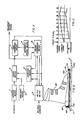
- Figure 1 is a schematic diagram of a light-activated dual axis detector and associated signal processing and balancing circuitry according to an embodiment of the present invention.
- Figure 2 is a timing diagram for pulsed detector apparatus according to an embodiment of the present invention.
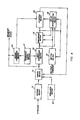
- Figure 3 is a block diagram of an electronic balancing means according to an embodiment of the present invention.
- Figure 4 is a block diagram of another electronic balancing means according to an embodiment of the present invention.
- Figure 5 is a schematic diagram of an embodiment of an electronic balancing means according to the block diagram of Figure 4.
- Figure 6 is a schematic side view of various embodiments of a detector according to the present invention incorporated into a safety ski binding.
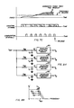
- Figure 7A is a schematic diagram of an embodiment of a capacitive dual axis detector according to the present invention.
- Figure 7B is a schematic diagram of circuitry for use with a capacitive dual axis detector according to an embodiment of the present invention.
- Figure 7C is a timing diagram for one embodiment of processing circuitry that may be used with a capacitive embodiment of the detector according to the present invention.
- Figure 8A is a schematic diagram of an alternative embodiment of circuitry for use with a capacitive detector.
- Figure 8B is a response diagram of a low-pass filter such as used in the circuitry embodiment of Figure 8A.
- Figure 9A is a schematic diagram of a dual axis resistive detector according to an embodiment of the present invention.
- Figure 9B is a schematic diagram of circuitry for use with a dual axis resistive detector according to an embodiment of the present invention.
- Figure 10A is a schematic diagram of a dual axis Hall Effect detector according to an embodiment of the present invention.
- Figure 10B is a schematic diagram of circuitry for use with a dual axis Hall Effect detector according to an embodiment of the present invention.
- FIG. 1 there is shown a schematic diagram of one preferred embodiment of the present detector invention including as a source element a light source 1 and as a sensing element a photosensor 3 comprising four, mutually electrically isolated, photosensitive regions, A, B, C and D. While each of those regions is shown in Figure 1 as being of the same shape and area, i.e., a quarter of a circle, and as having generally perpendicular boundaries, the invention is not limited to a detector having a sensing element with similarly shaped sensing regions or lying in a single plane. Some applications may require that all of the sensing elements, whether more or less than four, not be of the same size and shape and/or that the division between them not intersect at substantially, right angles.
- the photosensitive regions are shown to be formed on a substantially planar substrate.
- the sensing element, here photosensors, for example could be discrete photocells fixed to numerous locations on a three-dimensional surface.
- the present description discusses only the preferred embodiments of the invention, that is, sensing elements employing four sensing regions, each having substantially the same shape and area, with mutual boundaries intersecting at substantially right angles. In these preferred embodiments, the quadrants are contiguous, although electrically mutually isolated.
- each region is a separate photosensor and, as is preferable, all the photosensors are fabricated on a single substrate.
- Light source 1 may be any compact light source having a long life, and, preferably, a fast response time relative to any modulation of light source 1.
- Light source 1 is preferably a solid state light emitting diode (LED), which may be a laser. Its light output need not be visible.
- the four regions of photosensor 3 are preferably solid state photosensors having a high sensitivity to the wavelengths emitted by source 1. The extent of the illumination of photosensor 3 by light source 1 is limited by an iris 5 interposed between the light source and photosensor 3, to the area shown by cross-hatching in Figure 1. That area is shown as rectangular in Figure 1, but the iris opening could have other shapes.
- Light source 1 is mounted on one body, the relative motion of which is to be sensed and photosensor 3 on another or reference body.
- photosensor 3 moves with respect to light source 1
- the amount of light falling on quadrants A-D changes resulting in changes in the photovoltages or photocurrents produced by at least some of the photosensors. For example, if photosensor 3 moves in the direction of the line separating regions A and C from regions B and D, toward regions A and B, the amount of light falling on regions A and B will decrease because of the shadow cast by iris 5 and there will be an increase in the amount of light falling on regions C and D.
- Photosensor 3 may be fabricated by conventional means such as by depositing on a substrate a photosensitive material or by conventional integrated circuit techniques. Because these fabrication techniques permit construction of regions of relatively small dimensions, a high degree of sensitivity to the relative movement of photosensor 3 and light source 1 can be obtained. An "amplification" of movement sensitivity can be achieved by increasing the separation of the photosensor and light source, although increasing the separation increases the electronic noise produced by ambient mechanical vibrations and increases the precision with which iris 5 must be formed and positioned. A pair of electrical leads must be provided to each photosensitive region, although the lead to each region which is attached to a power source, may be common to all the regions. In Figure 1 this common connection is indicated by the ground connection of the substrate which supports the regions.
- FIG. 1 An embodiment of a measuring means applicable to the photosensor embodiment detector of Figure 1, for interpreting changes in electrical values as motions, is also shown in Figure 1.
- region A is shown connected through a resistor R2 to the negative sense input terminal of a difference amplifier A1, an embodiment of a measuring means, which has a feedback resistor R4 connected between its output terminal and negative sense input terminal.
- Region B is connected to the same input terminal through a resistor R6.
- Regions C and D are connected through resistors R8 and R10, respectively, to the positive sense terminal of amplifier A1, which is shunted to ground through resistor R12.
- the magnitude of the output signal of amplifier A1 is proportional to the difference between the signals at its input terminals.
- the output signal, V y of A1 is proportional to [(C+D) - (A+B)].
- V y increases indicating a relative movement in a particular direction.
- the amount of the increase in V y indicates the magnitude of the movement.
- relative movements along the X axis may be detected by an analogous measuring means.
- regions A and C are connected through resistors R14 and R16, respectively, to the negative sense input terminal of a difference amplifier A2.
- Regions B and D are connected through resistors R18 and R20, respectively, to the positive sense terminal of amplifier A2, which is also shunted to ground through resistor R22.
- Difference amplifier A2 has a feedback resistor R24 connected between its output terminal and negative sense input terminal.
- the output signal, V x , of amplifier A2 is proportional to [(B+D) - (A+C)]. That signal discloses the direction and magnitude of movements along the X axis. Because of the high input impedance of difference amplifiers A1 and A2, it is possible to have both connected at the same time, i.e., to simultaneously detect both X and Y axis changes. If, as is preferred, regions A-D are formed simultaneously in or on the same substrate, they will preferably have essentially identical electrical characteristics.
- resistors R2, R6, R8 and R10 and resistors R14 , R16, R18 and R20 may all be of the same value
- resistors R4 and R24, R12 and R22 may have the same values
- amplifiers A1 and A2 may have essentially identical characteristics, if totally balanced operation is desired. In that event, it is convenient to produce such matched components by forming all these elements in a single integrated circuit. However, if one of the X and Y axis signals is to be emphasized over the other, then the amplifiers and resistors in the X and Y signal circuits will not have identical values and characteristics.
- V x and V y it is convenient to form the circuitry for processing the V x and V y as a hybrid circuit, mounted on the rear of the substrate bearing regions A-D. Such an arrangement serves to lower costs, reduce size and weight and improves reliability.
- Figure 1 includes within the dashed lines designated I, an embodiment of a signal selection means for selecting and transmitting the larger of the amplified V y and V x signals. Through the signal selection means the larger and/or more significant of the processed V y and V x signals may be selected. First, the signals are rectified so that their absolute magnitudes may be compared and then the signal having the larger absolute magnitude is selected. The output signal from amplifier A1 is applied through a resistor R26 to the negative sense input terminal of an inverting amplifier A3.
- the positive sense input terminal of amplifier A3 is grounded.
- the anode of a diode D1 is connected to the output terminal of amplifier A3.
- the cathode of diode D1 is connected to a feedback resistor R28, which is also connected to the negative sense input terminal of amplifier A3, and to the positive sense input terminal of a voltage follower amplifier A4.
- the output terminal of amplifier A4 is connected to the anode of a diode D2.
- the cathode of diode D2 serves as an output terminal and is also connected to the negative sense input terminal of amplifier A4.
- amplifier A3 and diode D1 function as a rectifying means. If V y is negative, the output signal of amplifier A3 is positive (because of the inverting effect A3), readily passes through diode D1 and is applied to the positive sense input terminal of amplifier A4. If V y is positive, the output signal of amplifier A3 is negative, and is blocked by diode D1. Therefore, the positive V y reaches the positive sense terminal of amplifier A4 through input resistor R26 and feedback resistor R28. That is, the circuitry insures that a positive sense signal is always present at the positive sense input terminal of amplifier A4.
- V x Similar circuitry is provided for the V x signal comprising an input resistor R30 to the negative sense input terminal of an inverting amplifier A5 which has its positive sense input terminal grounded.
- the anode of a diode D3 is connected to the output terminal of amplifier A5.
- the cathode of diode D3 is connected to a feedback resistor R32 and to the positive sense input terminal of a voltage follower amplifier A6.
- Resistor R32 is also connected to the negative sense input terminal of amplifier A5.
- a negative sense V x passes through amplifier A5 and diode D3 and is applied to the positive sense input terminal of amplifier A6.
- a positive sense V x is blocked by diode D3, but passes through resistors R30 and R32 to the positive sense input terminal of amplifier A6.
- a positive sense signal is always applied to the positive sense input terminal of amplifier A6.
- the output signal of amplifier A6 is connected to the anode of a diode D4, the cathode of which serves as an output terminal and is connected to the negative sense input terminal of amplifier A6.
- the cathodes of diodes D2 and D4 are connected together and at their junction form the output terminal of the signal selection means.
- V x and V y signals causes the output signal of either amplifier A4 or amplifier A6 to become negative, the negative signal being blocked by either diode D2 or diode D4.
- V o appears at the common junction of diodes D2 and D4.
- a sample and hold network comprises an electronic switch SW2, to which V o is applied, the output of which is connected to the positive sense terminal of a voltage follower amplifier A7. That positive sense terminal is shunted to ground through a capacitor C2.
- the negative sense input terminal of amplifier A7 is connected to its output terminal, at which the sampled V o signal appears.
- Light source 1 is powered from a power source designated V1, through a load resistor R L , which limits the current flowing through the light source, the other terminal of the light source being grounded.
- Light sources are well known to consume relatively large currents which is undesirable in battery powered circuits because of the rapid depletion of the battery. Accordingly, Figure 1 includes an embodiment of a pulse mode or power conservation means for reducing the average power consumption of the source means.
- the embodiment of the pulse mode means circuitry includes a series-connected switch SW1 and resistor R1 interposed between power source V1 and load resistor R L .
- a grounded capacitor, C1 is connected at the junction of R1 and SW1.
- a train of timing pulses is applied through an optional OR gate G1 (the function of which is explained later herein) to switch SW1 and switch SW2 of the sample and hold network, closing and opening them respectively, at the beginning of each chopping pulse.
- G1 the function of which is explained later herein
- switch SW1 closes, capacitor C1 discharges causing light source 1 to emit light.
- switch SW2 closes connecting amplifiers A4 and A6 to amplifier A7 and capacitor C2 charges to the larger of output signals V x and V y .
- both SW1 and SW2 open so that capacitor C1 charges again, and the larger of output signals V x and V y is stored in capacitor C2.
- Capacitors C1 and C2 are selected to have sufficient capacity so that the decrease in voltage during their respective discharges is within acceptable units. Between chopper pulses, C1 accumulates sufficient charge to power light source 1 when SW1 is closed so as to avoid a surge of current from the power source when the next chopper pulse begins. Capacitor C2 charges during a chopper pulse and maintains between chopper pulses approximately the same signal voltage at the input of amplifier A7 that was present at the end of the previous pulse. That is, the source element signal and the output signal generated by the measuring means are synchronously switched into and out of operation by the pulse mode means.
- the chopper signal pulse duration and interval are chosen so that the chopper pulse rate, i.e., the sample rate, has a period of not more than one-tenth of the fastest expected time variation of the quadrant signals. If signals varying no faster than 10 milliseconds over the desired range are expected, a sample rate of 1 kHz is satisfactory. A sample period of about one per cent of the sample rate yields satisfactory results. For this example, a chopper pulse duration of 5 to 10 microseconds would be satisfactory. As an example of the power savings with pulsed operation, consider a light source having an average normal current flow of 10 milliamperes.
- the average current consumed by the light source is reduced to 50 microamperes. That is, the average power consumption of the light source is reduced by a factor of 200.
- the total power consumption of the detector and processing circuitry may be reduced to the micropower range.
- timing diagrams show the effect of pulsing the detector for the embodiment and example just described.
- a chopper signal pulse train is shown.
- a diagram of the stimulus signal applied to the detector is shown in the middle graph.
- the dashed lines indicate the level of the stimulus signal sampled during the chopper pulse.
- the sampled signal at the sample and hold network output is shown.
- Figure 2 shows the value of the stimulus signal during each chopper pulse that is sampled and stored on capacitor C2 until the update provided by the next sampling interval. While the input signal to amplifier A3 is therefore a series of amplitude modulated pulses, the sampling is rapid enough that no significant variations in the detected signal are missing from the sampled signal that is applied to follower amplifier A7.
- the output signals of amplifiers A1 and A2 may not be zero as desired in the initial or static condition, when the detector elements have not yet moved with respect to each other.
- This imbalance is generally attributable to misalignment of light source 1, photosensor 3 and iris 5.
- a balancing means for nulling the output signal may include mechanical balancing means, such as adjustable mounting screws bearing on the two detector elements for aligning them with respect to each other. If the electronic components are mismatched, it may be impossible to establish a null point mechanically. In addition, mechanical alignment of two axes is difficult since adjustment of one generally affects the other. Therefore, it is desirable that the balancing means include electronic balancing means for electronically nulling the measuring means output signals. Preferably, the electronic balancing means is activated after a rough mechanical alignment of the detector elements has been achieved.
- the balancing means achieves a zero or near zero output signal by adding a variable magnitude signal to the quiescent sense signal. Both signals are applied to an adding means for algebraically summing the signals to produce a summed output signal. As the magnitude of the variable signal changes, so does the summed output signal which is compared to a reference signal having a near-zero magnitude.
- a comparator means for comparing the magnitude of the summed output signal and the reference signal directs the variable magnitude signal source to halt its magnitude changes when the magnitude of the summed signal is sufficiently close to zero.
- Figure 3 shows a block diagram of an embodiment of an electronic balancing means suitable for use with detector measuring means of Figure 1 or with any other electronic transducing system producing an analog electrical output signal in response to a stimulus.
- the technique is applicable to digital systems as well if the comparison means signifying a balance condition is performed in the digital domain rather than the analog domain.
- the electronic balancing means of Figure 3 nulls the output signal of the measuring means or transducing system when no intended stimulus is present by adding a balancing signal to the output signal to produce a summed ouput signal having a near-zero magnitude.
- the magnitude of the balancing signal varies with time, preferably monotonically during a balancing cycle, and is preferably produced digitally.
- the balancing means of Figure 3 comprises a sensing means 11 for receiving a stimulus to be measured and converting it into an analog electrical signal, i.e., a signal having an amplitude varying in relation to the magnitude of the stimulus.
- Sensing means 11 may be a photosensitive detector as described in connection with Figure 1, or any other embodiment of a detector in accordance with the present invention, a bridge circuit in which one or more of the bridge arm elements changes in electrical value in response to the stimulus, or some other analog or digital transducer.
- a counting means 13 produces a counting signal changing stepwise in magnitude with time, but changing in only one direction during a particular balancing cycle, which is applied to an adding means 15.
- the sensing signal is algebraically added to the counting signal to produce a summed output signal.
- the output signal of sensing means 11 is not zero, the addition of the balancing signal of appropriate magnitude reduces the summed output signal to nearly zero.
- the summed output signal is supplied to a first comparison means 17 for comparing the magnitude of the summed output signal to the magnitude of a balance reference signal produced by a reference signal means 19.
- the magnitude of the balance reference signal is near zero relative to the stepwise magnitude changes in the counting signal.
- the magnitude of the balance reference signal is more than that of one step, but less than that of two steps of the counting signal.
- comparison means 17 disables counting means 13 so that its output signal remains steady and ends the balancing cycle by signaling a switch means 21.
- Application of a balancing command to switch means 21, enables the balancing means and causes a balancing cycle to begin. If counting means 13 may count only in one direction, i.e., if the magnitude of the counting signal can only increase or decrease stepwise with time, rather than sometimes increasing, sometimes decreasing, then the output signal of switch means 21 is applied to counting means 13 to reset the counting signal to zero.
- An optional imbalance means 23 generates an imbalance signal which is applied to adding means 15 and forms part of the summed output signal.
- Imbalance means 23 ensures that the summed output signal has a greater absolute magnitude than and the same polarity or sense as the balance reference signal when the counting or balance signal is reset to zero. Imbalance means 23 avoids the possibility that a false null might occur by preventing the magnitude of the sensing means signal from being less than that of the balance reference signal should those two signals have opposite polarities. If counting means 13 may count in either direction. i.e., if the magnitude of the counting signal may change stepwise either increasing or decreasing with time depending upon the state of an up-down signal supplied to the counting means, optional imbalance means 23 would not be present.
- a balance command applied to switch means 21 results in a switch signal being applied to and initiating a second comparison means 25 which receives the summed output signal and the balance reference signal. If the absolute magnitude of the summed output signal exceeds that of the balance reference signal in either direction, second comparison means 25 generates an up-down signal having the proper logical state to achieve a balance condition so that the up-down signal is applied to counting means 13 for establishing the direction of counting during a balance cycle so as to reduce the absolute magnitude of the summed output below that of the balance reference signal. If the absolute magnitude of the summed output signal does not exceed that of the balance reference signal, second comparison means 25 does not generate an "up” or "down” command, but rather signals switch means 21 to terminate the balancing cycle.
- a balance command applied to switch means 21 results in the counting signal being reset to zero.
- the static sensing means signal is added in adding means 15 to the imbalance signal to produce a summed output signal having a magnitude exceeding that of the balance reference signal.
- the counting signal begins increasing stepwise in absolute magnitude reducing the absolute magnitude of the summed output signal stepwise.
- comparison means 17 signals switch means 21 to reset ending the balancing cycle and halting counting means 13. The magnitude of the counting signal is then "frozen", so that the nulled summed output signal is nearly zero, relative to the magnitude of the balance reference signal.
- a balance command to switch means 21 initiates second comparison means 25. If the absolute magnitude of the summed output signal does not exceed that of the balance reference signal, switch means 21 terminates the balancing cycle as explained before. If the balancing cycle is not terminated, the polarities of the summed output signal and of the balance reference signal are compared in second comparison means 25. As a result of that comparison an up-down signal is generated setting counting means 13 to begin increasing or decreasing stepwise the magnitude of its counting signal, beginning at the magnitude where it last stopped counting. The change in counting signal magnitude reduces or increases the magnitude of the summed output, as necessary, so that its magnitude converges toward that of the balance reference signal.
- counting means 13 is triggered by the sense of the up-down signal to count in the necessary direction to increase the magnitude of the summed output signal until its absolute magnitude is less than that of the balance reference signal.
- Comparison means 17 signals the end of the balancing cycle, as before, freezing the magnitude of the counting signal.
- the circuitry shown within the dashed lines II is an embodiment of the electronic balancing means of Figure 3 having a single direction counting means.
- Balancing means circuitry is shown in Figure 1 connected only to the V y signal circuitry, but identical circuitry would be connected to the V x signal circuitry, for independent nulling of the V x signal. Since the V x balancing means circuitry would be the same as the V y balancing circuitry, there is no need to separately depict and describe it.
- one skilled in the art can apply the balancing circuitry of Figure 1 to detectors having greater or fewer than four sensing regions.
- the negative sense input terminal of a comparator A8 is connected to the cathode of diode D1.
- a variable reference signal means 7 for producing a balance reference signal V BALREF .
- the output terminal of comparator A8 is connected through a capacitor C3 to a reset terminal R FF of a flip-flop FF1.
- a grounded resistor R34 is also connected to the flip-flop reset terminal, C3 and R34 forming a differentiator.
- a terminal L of flip-flop FF1 receives a balance command given either manually or automatically.
- Flip-flop FF1 normally has a low level or zero logic signal at an output terminal Q.
- Counter 9 begins when the input signal at terminal E r switches to a logical one and continues at the frequency of the clock signal until a logical zero is received at the enabling terminal E r .
- a resistor network 10 functioning as a digital-to-analog signal converting means is attached to each of the output terminals of counter 9.
- One terminal of a resistor in network 10 is connected to each of the output terminals of counter 9 and the other terminals of the resistors in the network are connected together so that a signal corresponding to the analog sum of the binary output signals of the counter is obtained at the common terminal of the resistors.
- counter 9 and resistor network 10 correspond to counting means 13 of Figure 3.
- the analog counting signal is applied to the negative sense input terminal of a differential amplifier A9.
- a feedback resistor R38 couples the negative sense input terminal to the output terminal of A9.
- An imbalance signal, V REF is applied to the positive sense input terminal of amplifier A9.
- the output signal of A9 is coupled through resistor R40 to the negative sense input terminal of difference amplifier A1.
- Flip-flop FF1 acts as a switch means enabling the electronic balancing means and resetting counting means 9.
- a balance command i.e., a logical one
- the output signal at terminal Q switches to a logical one enabling counter 9.
- the output of counter 9 is cleared to zero by the differentiated pulse that reaches reset terminal R r .
- the input signal to the negative sense terminal of amplifier A9 goes to zero, so that the output signal of A9 becomes positive by an amount determined by the value of V REF , the imbalance signal, and the gain of amplifier A9 with feedback resistor R38.
- Counter 9 begins counting upwards in response to the clock signal pulses.
- Amplifier A9 and signal V REF function as the optional imbalance means insuring that initially there is an imbalance condition, i.e., a non-zero output signal of the measuring means, at the positive sense input terminal of A8. (V REF reaches that latter point by passing through A1 and A3).
- V REF reaches that latter point by passing through A1 and A3.
- Amplifier A9, with resistor R38 produces the algebraic sum of the signals applied to its input terminals, i.e., the difference of the counting signal and V REF , a signal that decreases in magnitude with time.
- the algebraic sum signal is added to the imbalanced output signal of A1, through A1, and resistor network R40 and R4, which function as an adding means, to produce a summed output signal.
- Comparator A8 functions as a comparison means for comparing the summed output signal (which at the negative input terminal of A8 decreases in magnitude with time by virtue of being inverted by A3) to V BALREF and for disabling counter 9 through flip-flop FF1 when the magnitude of the summed output signal falls below the magnitude of V BALREF . At that time, the output signal of A8 switches from a low to a high state sending a pulse to reset terminal R FF of flip-flop FF1.
- the signal at the Q output terminal then switches to a logical zero, disabling counter 9 and the balancing means, thereby "freezing" in place the signal to the negative sense input terminal of comparator A8. That is, a null point balance, a summed output signal from A3 having a near-zero magnitude relative to the magnitude of the balance reference signal, which is now the effective measuring means output signal, is achieved by adding the balancing signal from A9 to the output signal of the measuring means. Obviously, the magnitude of V REF must be sufficient to cause an imbalance in the output signal of amplifier A1.
- V BALREF is variable and is chosen to produce a null, i.e., an output signal from amplifier A3 having a magnitude acceptably near zero, and is greater than one, but preferably less than the magnitude of two steps of the counting signal.
- the embodiment of the balancing circuitry shown has the advantage that a digital signal, less susceptible to noise than an analog signal, forms part of the null bias. Thus, the stability of the null point depends in large measure on the stability of V REF .
- the electronic balancing means of Figure 3 and the embodiment of Figure 1 may be used for nulling output signals of any electronic sensing apparatus by producing a summed output signal.
- the counting signal may be capable of changing stepwise in magnitude with time or in one or both directions, but changes only in one direction during a particular balancing cycle.
- the imbalance means must insure that upon enablement of the balancing means, the output signal to be nulled has the same polarity or sense as, and a greater absolute magnitude than, the balance reference signal.
- FIG 4 a block diagram of an alternative electronic balancing means is shown.
- a stimulus is applied to a sensing means or transducer 111 for producing an analog electrical signal varying in magnitude in relation to the magnitude of the stimulus. That analog signal is applied to an adding means 113 as is the balancing signal explained hereinafter.
- the algebraic sum of those input signals is the summed signal that is applied to a first comparison means 115 for comparison in magnitude to a balance reference signal generated by a reference signal means 117.
- a coincidence means 119 receives as input signals the output signal of comparison means 115, an enabling signal from a switch means 121 and a delay signal from a delay interrogating means 123.
- the output signal of switch means 121 which enables the balance means, enables delay interrogating means 123.
- Delay interrogating means 123 establishes a delay period at the end of which, if the sensed stimulus signals have remained quiescent during the delay period, generates the delay signal. That delay signal is transmitted to a counting means 125, if that counting means may count in only one direction, for resetting that counting means.
- Delay interrogating means 123 also receives as an input signal the output signal of comparison means 115.
- the output signal of coincidence means 119 is connected to an enabling terminal of counting means 125.
- Counting means 125 produces a counting signal which changes stepwise in magnitude in time in one direction during a balancing cycle.
- the counting signal is the balancing signal which is added in adding means 113 to produce the summed output signal.
- the output signal of an optional imbalance means 127 is applied to adding means 113 and is part of the summed output signal if counting means 125 is capable of counting in only one direction. If counting means 125 is capable of counting either "up” or “down” depending on the logical state of an up-down signal applied to a counting means triggering terminal, imbalance means 127 would not be present and no connection between delay means 123 and counting means 125 would exist. Rather, a second comparison means 129 would receive the balance reference signal and summed output signal. The output of second comparison means 129 is connected to counting means 125 to establish the logical state of the up-down signal and, therefore, the proper direction of counting so that a balance may be achieved.
- a balancing cycle is commenced by the application of a balance command at switch means 121 which sends a logical one signal to one input of coincidence means 119 and activates delay interrogating means 123.
- Comparison means 115 provides another logical one signal to coincidence means 119 when the signal to comparison means 115 exceeds the balance reference signal.
- a third logical one signal necessary to commence balancing is provided by delay interrogating means 123 after a fixed delay period. With a counting means capable of counting in only one direction, that delay signal also resets the counting signal to zero. With a counting means capable of counting in either direction, the polarities of the summed output signal and balance reference signal are compared in second comparison means 129.
- the signal from first comparison means 115 to coincidence means 119 never goes high and a balancing cycle is postponed. If the summed output signal magnitude is greater than that of the balance reference signal, the comparison means 129 generates an up-down signal having the proper logical state to achieve a balance condition.
- the up-down signal sets counting means 125 to count in the proper direction so that the counting signal causes the absolute magnitude of the summed signal to approach and eventually fall below that of the balance reference signal, ending the balancing cycle.
- coincidence means 119 When the three logical ones are present at its input, coincidence means 119 enables counting means 125.
- the counting signal then changes stepwise in magnitude with time, either from zero, if reset, or from the previous count, if the counting means is capable of counting in either direction, changing the magnitude of the input signal to adding means 113 and, thereby, to comparison means 115.
- Comparison means 115 compares the absolute magnitude of the summed output signal (its input signal) to that of the balance reference signal. When the absolute magnitude of the summed output signal falls below that of the balance reference signal, marking the end of a balancing cycle, the output signal of comparison means 115 switches logical states thereby signalling coincidence means 119 to switch and disable counting means 125.
- coincidence means 119 also resets switch means 121 and delay interrogating means 123.
- counting means 125 can produce a stepwise increasing or decreasing magnitude counting signal so long as its ultimate effect at the output of adding means 113 is to converge the absolute magnitude of a summed signal exceeding that of the balance reference signal toward zero.
- the polarity or sense of the balance reference signal generated by reference signal means 117 must obviously be coordinated with the direction of change and polarity of the counting signal.
- the reference balance signal has a magnitude near zero relative to the stepwise changes of the counting signal, and, preferably, is greater than one, but less than two, of the counting signal steps.
- Imbalance means 127 ensures that the summed output signal has, upon enablement of the balancing means, the same polarity as, and a greater absolute magnitude than, the balance reference signal to which it is compared. Thus, the counting signal will be certain to cause the summed output signal to converge, provided the proper signal polarities are observed.
- connection of the output signal of first comparison means 115 to the reset terminal of delay interrogating means 123 ensures that balancing can take place only if the sensing means signal is quiescent.
- Coincidence means 119 cannot enable counting means 125, i.e., initiate a balancing cycle, until the delay signal is received from delay means 123. That delay signal is generated after the passage of the time interval or delay period established by delay means 123 and started when a balance command is received from switch means 121. If a reset signal reaches delay means 123 during the timing of a delay period, the timing of the period begins again, as if never begun before. If the sensing means signal changes polarity with respect to V BALREF , i.e.
- coincidence means 119 is signaled on the changes in polarity and balance is repeatedly attempted until the sensing signal is quiescent, i.e. until delay means 123 is not reset during a complete prescribed delay period.
- FIG. 5 a further embodiment of the electronic balancing means of Figure 4 employing a counter capable of counting in a single direction is shown.
- the embodiment of the sensing means shown is a modified resistance Wheatstone bridge 201 having the usual opposing sensing terminals connected to the positive and negative input terminals of a difference amplifier A11.
- the bridge is modified by opening one of the usual opposing power supply terminals, the other terminal being grounded in the conventional manner.
- V REF corresponding to a stable power supply voltage
- the other arm is applied the balancing signal, the generation of which is described herein.
- the magnitude of the output signal of A11 is zero. But when the sensors are in their quiescent or static state, the output signal of A11 may not be zero if the elements are not matched or one or more is being subjected to an initializing stimulus. However, by adjusting the magnitude of the balancing signal, a near-zero output signal from A11 may be obtained, i.e., the output signal may be nulled or balanced.
- Figure 5 shows a bridge type resistive sensor merely for variety.
- the photosensor detector embodiment of Figure 1 can also be used with this embodiment of the electronic balancing means.
- One such circuit would be used for balancing each of the V x and V y signals as explained in connection with Figure 1.
- A11 of Figure 5 would correspond to amplifier A1 of Figure 1 and the input resistors R2 - R10 of Figure 1 would be connected to the input terminals of A11.
- a feedback resistor R42 is connected between the negative sense input terminal of A11 and its output terminal.
- the output signal of amplifier A11 is the summed output signal comprising the balancing signal and the quiescent sensor signal.
- the output terminal of A11 is connected to the positive sense input terminal of a comparator A12 corresponding to comparison means 115 of Figure 4.
- a balance reference signal, V BALREF generated by a reference signal means 203 is connected to the negative sense input terminal of A12.
- the output terminal of A12 is connected to the first of three input terminals of an AND gate G2 and through a capacitor C6 to a resistor R44, the opposite terminal of which is grounded.
- C6 and R44 form a differentiator, the ungrounded terminal of R44 being connected to the first of two input terminals of an OR gate G3.
- the output terminal of gate G3 is connected to a reset terminal R I of a delay counter 205.
- the output terminal O I of delay counter 205 is connected to the second of the input terminals of gate G2 and through a capacitor C7 to a grounded resistor R46, C7 and R46 forming another differentiator.
- the ungrounded terminal of R46 is also connected to a reset terminal R k of a digital counter 207.
- the third input terminal of gate G2 is connected to an output terminal Q of a flip-flop FF2 and to an enabling terminal E I of delay counter 205.
- the output terminal of gate G2 is connected to an enabling terminal E K of counter 207 and through a logic inverter I1, to one terminal of a capacitor C8.
- the other terminal of capacitor C8 is connected to the second input terminal of gate G3 and to a reset terminal R F of flip-flop FF2.
- R F is grounded through resistor R48.
- a switch SW4 shunted to ground through a resistor R50, is connected between the input of an inverter I2 and power source V2.
- the output terminal of I2 is connected to a first input terminal of an OR gate G4.
- An interval counting means 209 for periodically enabling the balancing means is connected to the other input terminal of a gate G4, the output terminal of gate G4 being connected to an enabling terminal N of flip-flop FF2.
- Delay counter 205 is activated by a high level Q terminal output signal which appears at input terminal E I .
- the delay counter then counts for a specified delay period, producing a high level delay signal at terminal O I , if no reset signal is received at terminal R I during the delay period. If a reset signal is received, the timing of the delay period begins again, as if a high level signal had just arrived at terminal E I .
- Delay counter 205 determines the delay period by counting pulses provided at an input terminal T I by a first clock signal, the conventional source of which is not shown.
- Delay counter 205 provides a means for timing the length of a fixed period and signaling the arrival of the end of that period unless the timing is interrupted, in which case the timing of the period starts over.
- Counter 207 produces signals in binary code at its output terminals corresponding to the number of counting intervals which have passed since the counting began. Counting begins when a high level signal is applied to enabling terminal E k and the total count is reset to zero when a pulse arrives at reset terminal R k . Counting is synchronous with a second clock signal, the conventional source of which is not shown, applied to a timing terminal T k . One terminal of each of a network of resistors 211 is connected to each of the output terminals of counter 207 and the other ends of the resistors are commonly connected. Resistors 211 function as a digital-to-analog signal converting means producing a signal having a magnitude that is the analog sum of the binary count.
- counter 207 along with resistor network 211 comprise a counting means corresponding to counting means 125 of Figure 4.
- the common connection of a resistor network 211 is connected to the positive sense input terminal of a voltage follower amplifier A13 which is grounded through resistor R52.
- the negative sense input terminal of A13 is connected to the output terminal of A13.
- Resistor R52 provides the summing junction for ladder network 211.
- the output of amplifier A13 is the balancing signal which is connected to one of the opened arms of bridge 201 as earlier explained, or through a load resistor to the negative sense input terminal of A11 if the circuit is used with a detector, such as the quadrant detector of Figure 1.
- a balancing cycle is initiated by applying a balancing command to flip-flop FF2.
- the command can come either from the opening of switch SW4 disconnecting the power source from inverter I2 or from a pulse generated by interval counting means 209. A pulse from either of these sources results in a high signal at input N of flip-flop FF2.
- Flip-flop FF2 then acts as the switch means 121 of Figure 4 enabling the electroncic balance means by sending a high signal to the enabling terminal E I of delay counter 205 and to the third terminal AND gate G2.
- AND gate G2 acts as coincidence means 119 of Figure 4 enabling counter 207, when the balancing means is enabled, when the delay signal is generated by delay counter 205 and when the summed output signal, i.e., the input signal to comparator A12, has a magnitude exceeding the magnitude of the balance reference signal.
- the enablement of delay counter 205 causes it to begin the timing of a delay period, at the end of which a high level signal appears at its output terminal O I and at the second terminal of AND gate G2.
- the switch of the signal at O I to the high level also resets the output of counter 207 to zero causing an imbalance condition, i.e., a high level signal appears at the output of comparator A12 and therefore at the first input terminal of gate G2.
- delay counter 205 when enabled by flip-flop FF2, acts at the end of an uninterrupted delay period to reset counter 207 to zero and to enable one input gate G2.
- the resetting of the counting signal to zero causes the output signal of A11 to become positive as a result of the presence of V REF , thereby switching the output signal of comparator A12 to the high level and placing a high level signal at the first input terminal of gate G2.
- Gate G2 when enabled by the coincidence of three high level signals at its input terminals, enables counter 207 which begins generating an increasing digital counting signal, the analog equivalent of which is the balancing signal appearing at the output signal of A13. That increasing balancing signal causes the signal at the positive sense input terminal of comparator A12 to decrease.
- the output signal of A12 switches from high to low, switching the output of gate G2 to the low state and thereby disabling counter 207, through terminal E k , from changing its output signal. That is, the magnitude of the balancing signal is frozen and the summed output signal is nulled, i.e., its magnitude is less than V BALREF .
- the counting or balancing signal, V REF and the static sensor signal are all algebraically added through A11 acting as an adding means to produce the summed output signal, i.e., now the balanced or nulled output signal.
- the transition in the output signal of gate G2 is inverted by inverter I1 and passed through to terminal R F of flip-flop FF2, resetting it in preparation for receiving the next balance command.
- the reset causes the output signal at the Q output terminal of FF2 to drop to the low state disabling delay counter 205.
- the same signal passes through gate G3 to reset delay counter 205 through its reset terminal R I .
- the sensing means changes polarity with respect to V BALRED , i.e. generates at A11 a signal first falling below and then exceeding V BALREF in magnitude, the sensor signal is not quiescent and balancing would be inappropriate. In that case, the output signal of A12 momentarily goes high when V BALREF is exceeded and a differentiated pulse reaches and resets delay counter reset terminal R I via gate G3. Then the timing of the delay period begins again.
- this embodiment of the electronic balancing means insures that the sensed signal is quiescent or static by sampling it for the delay period before attempting to null the summed output signal from A11.
- V REF ensures that when the balancing signal falls to zero, the magnitude of the output signal of A11 will be of the same polarity and greater magnitude than V BALREF . That is, V REF and part of the sensing means act as an imbalance means producing an imbalance signal insuring that the summed output signal upon enablement of the balancing means has the same polarity and a greater magnitude than the balance reference signal. If this balancing means embodiment is used with the photosensor detector embodiment of Figure 1 as a sensing means, an optional imbalance means would be added as already explained for that embodiment. That is, an imbalance source V REF would be supplied, independent of the sensing means, to A11 to insure the initial imbalance.
- the embodiment of Figure 5 provides for either manual enablement of the electronic balancing means by the opening of SW4 or by periodic automatic enablement whenever interval counter 209 emits a pulse. It is intended that a balance cycle be activated as frequently as necessary to compensate for component value drift considering the environment in which the circuit is used, either manually, or in default of that, automatically.
- the counting signal reduce the absolute magnitude of the summed output signal to below the absolute magnitude of the balance reference signal at which point a nulled or balanced summed output signal is achieved.
- both a pulse mode. i.e., power-conserving, means and electronic balancing means are used, as in the inventive embodiments of Figure 1, their operations must be coordinated to obtain the desired results.
- Either the chopper pulses and clock signal pulses driving the counting means must be synchronized so that balancing may be completed during the "on" time of one chopper pulse or the chopper pulses must be disabled during balancing to ensure the operations of the source means during the entire balancing cycle.
- the clock signal and chopper signal would be derived from the same timing oscillator.
- gate G1 does not interfere with sampling when balancing is not taking place since a "high" chopper signal means a high G1 output signal operating SW1 and SW2 as described before.
- the electronic balancing means of Figure 5 applied to the detector embodiment and associated circuitry of Figure 1, the enabling signal to be applied to gate G1, along with the chopper signal, would be taken from the output of AND gate G2.
- switch SW3 in parallel with resistor R1.
- switch SW3, like gate G1 is connected to the enabling terminal of counting means so that SW3 is closed during the balancing cycle.
- SW3 would be closed when the output signal of gate G2 is high.
- the current provided to light source 1 during balancing is uniform and slightly increased over the flow during sensing operations of the circuitry. That increased current flow is so brief (e.g., 1/2 millisecond) that no material increase in overall power consumption results from the longer balancing cycle with the lower clock signal frequency.
- a safety ski binding As described in my U.S. Patent 4,291,894, the function of a safety ski binding is to sense during skiing the presence of forces on a skier's foot, leg and boot, and to release the ski from the boot when those forces reach dangerous levels so as to avoid injury to the skier. Safety bindings therefore have a latching condition in which the binding is firmly locked to a skier's boot and a releasing condition in which the binding is released from the boot.
- Mechanical safety bindings are known in the art, but electronic safety bindings having electrical force sensing and electronic processing of electrical force signals to trigger binding release, provide significant advantages as further described in U.S Patent 4,291,894.
- FIG. 6 there is shown in highly schematic form a side view of a ski boot 301 held on a ski 303 by safety ski binding including toe and heel boot releasing latches 305 and 307, respectively.
- the sole of boot 301 is received by and clamped to a sole plate 309 rigidly affixed to an elastic spacing means 311.
- a rigid ski plate 312 is affixed to elastic spacing means 311 opposite sole plate 309 and is firmly attached to ski 303.
- a detector sensing means including sensing element 313 is rigidly mounted to ski plate 312, and a detector source means including source element 315 is rigidly mounted to sole plate 309.
- the relative locations on ski and boot of the source and sensing means may be interchanged.
- sensing element 313 may correspond to photosensor 3 and source element 315 may correspond to light source 1.
- Figyre 6 are the circuitry and power source previously described, the signal processing circuitry and interconnected release triggering mechanism for releasing the ski from the boot or the housing to protect the detector. Embodiments of such circuitry and mechanisms are described above and in my U.S. Patent 4,291,894. During skiing, various forces are exerted on the ski boot as a result of turns, accelerations, decelerations, bumps, etc. In the embodiment of Figure 6, the forces between the ski and the skier's leg cause movement of boot 301 and sole plate 309 with respect to ski 303.
- Elastic spacing means 309 which may be a pad of an elastomeric material such as rubber or another resilient material, or a mechanical spring means, allows relative movement between the ski and boot in response to forces encountered during skiing, i.e., elastic spacing means 309 functions as a multidimensional spring.
- the relative movements of ski and boot are related to the forces between the ski and skier's leg so that in the ski binding application, the detector functions as a force sensor.
- the detector embodiment is a four region detector of the type described in reference to Figure 1, the detector sensing element 313 may be mounted with the boundary between two of the regions generally parallel to the skiing surface of the ski. In that configuration, torques twisting a skier's leg will generate changes in V x signals. Likewise, in that configuration, forces which tend to tip the skier in the direction of, or opposite to the direction of, travel of the ski will generate changes in V y signals.
- balancing is generally not required more than once or twice during a week of skiing.
- a balance command is preferably given manually or automatically at intervals when the sensed forces return to essentially the static condition. Any of the electronic balancing means previously described may be satisfactorily used in an electronic safety ski binding. With the embodiment of the balancing means shown in Figure 5 applied to a ski binding, switch SW4 comprises an activation means for applying a balance command.
- the activation means is triggered when a ski boot is removed from a binding incorporating the detector, assuring a rebalance at least once during each day of skiing. In this situation, there is no sensor signal attributable to the skier's weight or to skiing forces.
- interval counter 209 preferably emits a pulse about once every 16 days to insure that a balance condition is maintained even while the electronic binding is not in use. Otherwise, when a binding is first clamped onto a boot, a skier might start out with a measuring means that had become imbalanced through normal aging of the electronic and mechanical systems of the binding. While the interval counter arrangement requires power be perpetually applied to the binding, the total power consumption of the preferred detector and preferred CMOS circuitry is extremely small.
- the delay period for the electronic balancing means of Figure 5 in a ski binding application is preferably about three seconds. That delay period prevents a balancing cycle from beginning when a ski is bouncing after a release during skiing or when a skier first steps out of the binding. Rather, balancing is postponed until the sensed forces or impacts of the ski appearing as forces disappear for at least the delay period.
- the detector is not limited to light as source means and photosensors as sensing means, just as it is not limited to four sensing regions or devices.
- a capacitive embodiment 401 of a four region version of the detector is depicted.
- Four mutually electrically isolated regions or capacitor plates A, B, C and D are contiguous on a non-conductive substrate 403.
- Each area is metallic or formed of some high conductivity material forming one plate of a capacitor.
- each plate covers one quarter of substrate 403.
- Substrate 403 is separated by a dielectric 405 from a second non-conducting substrate 407 containing as a source element a conductive area 409, generally square in shape and smaller in area than the combined areas of plates A-D.
- Area 409 forms a second plate of the capacitor, that plate being common to all of plates A-D.
- a capacitive detector including four capacitors is formed.
- the mutual plate area of at least one of the capacitors is reduced, reducing its capacitance. Measurement of changes in the individual capacitances through leads connected to the common plate and to each of plates A-D allows a determination of the direction and magnitude of the relative movements of the plates in planes containing them.
- the plates In order to obtain the largest capacitance and largest capacitance changes, it is preferred that the plates have as large an area as a particular installation permits and that the dielectric separating substrates 403 and 407 be as thin as possible, yet have a low coefficient of friction to all movement of the plates.
- the dielectric may be air, it is preferred that a material with a higher dielectric constant be inserted between the plates.
- TEFLON is one material that is suitable as a dielectric in a capacitive embodiment of the detector since it has a low coefficient of friction and a relative dielectric constant of about 2.
- the capacitive plates When the dielectric is air, the capacitive plates may also move so as to widen and narrow the separation between them.
- the sum of capacitances A-D By measuring the sum of capacitances A-D, relative motion generally perpendicular to substrates 403 and 407 may be detected and measured, at the same time that relative motions in the planes of the substrate are measured. That is, embodiment of the detector shown in Figure 7A may be used to detect three dimensional movements.
- FIG 7B a simplified embodiment of a measuring means for a capacitive four region detector measuring two dimensional motions is shown. It is desirable to add conventional temperature compensation circuitry, such as temperature sensitive resistors or more complex circuitry including additional inverters, to stabilize the operation of the circuitry. Since such circuitry will be obvious to one skilled in the art, there is no need to depict and describe it.
- each plate has a corresponding capacitance associated with it, plate A has capacitance C A , plate B has capacitance C B , etc.
- each of those capacitances is used to determine the repetition rate of a pulse train generating oscillator comprised of an inverter with a
- Frequency-to-voltage means 501 may be, for example, any conventional frequency modulation detector. Frequency-to-voltage means 501 converts frequency f A to voltage V A . Similarly, means 503, 505 and 507 convert frequencies f B , f C and f D to voltages V B , V C and V D , respectively.
- V x and V y may then be combined in pairs by circuitry identical to that depicted to Figure 1 and described in connection therewith, to generate voltages V x and V y , indicated relative movements of the detector elements along the X and Y axes, respectively.
- signals V A and V B are applied through input resistors R64 and R66, respectively, to the negative sense input terminal of a difference amplifier A19.
- Signals V C and V D are applied through input resistors R68 and R70, respectively, to the positive sense input terminal of A19, which is grounded through resistor R72, Feedback resistor R74 connects the output terminal of A19 with its negative sense input terminal.
- V y proportional to [(V D + V C ) - (V A + V B )]
- V x proportional to [(V B + B D ) - (V A + V C )]
- Amplifiers A19 and A20 are entirely analogous to amplifiers A1 and A2, respectively, of Figure 1.
- Balancing means may be provided to balance the capacitive embodiment of the detector in its static state.
- the embodiments of an electronic balancing means shown in Figures 1 and 5 are directly usable with the capacitive detector circuitry shown in Figure 7B, as is the embodiment of the signal selection means shown in the dashed lines designated II in Figure 1.
- the pulses generated could be applied directly to digital counters for counting and summing. Further processing may be used to determine the relative motion of the detector elements.
- Figure 7C shows a timing diagram for one such technique for a ski binding application. The force experienced over time on a skier's leg is shown in the uppermost graph. The cumulative effect of an excessive level of force on a skier's leg is indicated by the shaded area under the curve. In the middle graph, the timing of a series of continuous "counting" intervals is shown. In the lower graph, the relative timing of "calculation" intervals, following the counting intervals, is shown.
- the pulse counters may be discrete or part of a microprocessor.
- Pulses from each oscillator may be counted by separate counters or, preferably, a single multiplexed counter may be used with serial access for each oscillator.
- pulses are counted for each oscillator, either in series or parallel, depending on whether multiplexing is used.
- the counting period must be much shorter than the period for response, which for a ski binding application is about 10 milliseconds. For such an application, the duration of the counting periods could be about 100 to 500 microseconds.
- the counted number of pulses is stored.
- a calculation interval runs, as shown in the middle diagram of Figure 7C.
- the pulse counts for each sensor accumulated during the preceding counting interval may be appropriately combined.
- the sum of pulse counts for regions A and B might be subtracted from the sum of the counts for C and D, much in the fashion used to calculate motion with the embodiment of Figure 1.
- a release signal is generated as schematically indicated at the right in Figure 7C.
- a microprocessor using such a technique may also include a large capacity memory that can vary the parameters of the release decision depending on skier skill, snow conditions, terrain, etc.
- automatic balancing of such a system may be accomplished by subtracting the quiescent pulse counts for each oscillator from the count accumulated during the counting period.
- Figure 8A shows an alternative embodiment of a measuring means for producing signals reflecting relative movements of the plates of a cpaacitive embodiment of the detector.
- a reference frequency signal, f REF generated by a stable frequency oscillator (not shown) is applied to each of four passive low-pass filters, each including a series-connected resistor and a parallel connected grounded capacitor.
- Each capacitor is one of the detector plate capacitors.
- the filter shown in the uppermost part of Figure 8A comprises a resistor R86 and a capacitor C A , the capacitor formed by plate A and the common plate.
- the signal appearing at the output of this filter has an amplitude V ' A (which is less than the amplitude of the input to the filter because the filter elements are selected so that the cut-off frequency is exceeded) and a frequency f REF .
- the other filters are formed with the other capacitors of the detector. The filter elements are chosen so that each filter has substantially the same cut-off frequency and the reference frequency is chosen to be above that cutoff frequency.
- An envelope detecting means 601 is connected to the output of the R86, C A filter.
- envelope detecting means 603, 605 and 607 are connected to the filters containing capacitors C B , C C and C D , respectively.
- the outputs V A -V D of means 601-607 correspond to the outputs V A -V D in Figure 7B.
- Figure 8B illustrates the linearized attenuation characteristic of a low-pass filter.
- the attenuation of the signal by the filter varies relatively rapidly with frequency.
- the output voltage from the filter containing C A is V ' A1 .
- the cut-off frequency of the filter changes shifting the response curve as suggested in Figure 8B by the dashed lines.
- An increase in capacitance causes a decrease in the cut-off frequency and vice versa.
- V ' A1 a different voltage, for example, V ' A2 or V ' A3 , is generated reflecting the movement and capacitance change.
- envelope detection means are used to demodulate the sensed information for further processing. These demodulated signals may be processed in the same manner as explained in connection with Figures 1 and 7 to generate V x and V y signals. Likewise, signal selection means and electronic balancing means can be used with the embodiment of detection circuitry shown in Figure 8A.
- Both the circuits of Figures 7B and 8A can be operated in a pulsed mode to reduce power consumption.
- a capacitive detector with CMOS processing circuitry in a ski binding application can be operated with a power consumption of less than 200 microwatts.
- the capacitive embodiment of the detector is particularly advantageously used with processing circuits such as are shown in Figures 7 and 8, because frequency dependent circuits lend themselves to easier realization with current CMOS technology than do amplitude dependent circuits.
- the capacitive detector embodiment is the most preferred detector for use in an electronic safety ski binding.
- the capacitive embodiment of a detector can be used in a ski binding just as described in connection with the photosensor embodiment of the detector.
- 315 represents the common plate of the capacitive detector and 313 the plate containing the quadrants.
- the relative positions of the detector elements may be interchanged.
- the description of the use of the photosensor embodiment of the detector in a ski binding is fully applicable to use of a capacitive embodiment and therefore it is unnecessary to repeat it.
- a resistive embodiment 701 of a four region detector comprises a non-conducting substrate 703 having deposited on it sheet resistive material to form mutually electrically isolated regions A, B, C and D.
- An electrical lead to each region is connected to one terminal of a voltage source and a lead from probe 705 is connected to the other.
- the resistance between the probe and each quadrant can be determined. That resistance is reflective of the relative position of the probe on the substrate.
- probe 705 and each quadrant may be connected to the terminals of a current source and the resistances between the probe and each of the quadrants determined by measuring the voltage drop along each path.
- Probe 705 must be able to slide over substrate 703 without abrasion or loss of electrical contact in spite of vibrations that the elements of detector 701 may experience. It is preferred therefore that a non-conductive lubricant be placed between probe 701 and quadrants A-D so that the two elements can be gently pressed together without a loss of sensitivity to the applied force.
- the resistances of quadrants A-D are preferably substantially identical, a condition that may be readily achieved using conventional thick film and integrated circuit technology.
- Amplifiers A21 through A24 are d.c. gain amplifiers each having a steady state voltage output which is a function of the value of the resistances connected to their negative sense input terminals and of the feedback resistances connected between their output terminals and negative sense input terminals.
- the resistance between probe 705 and region A i.e., R A
- R A is connected to the negative sense input terminal of amplifier A21 as is one end of feedback resistor R94 is connected to the output terminal of amplifier A21.
- the feedback resistors for each amplifier and amplifier gains are chosen to give the appropriate significance to the V x and V y signals, as discussed earlier.
- the entire amplifying network may be a hybrid circuit placed on the opposite side of substrate 703.
- the amplifier output signals reflecting the resistances measured for each region are then combined through differential amplifiers in the manner previously explained to produce V x and V y signals. That is, the signal produced by amplifier A21, and the signal produced by amplifier A22, are added through load resistors R102 and R104, respectively, and applied to the negative sense input terminal of difference amplifier A25. Similarly, the R C signal produced by amplifier A23, and the R D signal produced by amplifier A24, are added through load resistors R106 and R108, respectively, and applied to the positive sense terminal of difference amplifier A25.
- the output signal of amplifier A25 is then proportional to [(R C + R D ) - (R A + R B )] which is in turn proportional to the V y voltage described in connection with other embodiments of the quadrant embodiment of the detector.
- a V x signal is generated as shown by the other circuitry in Figure 9B wherein the R A and R C signals are combined through load resistors R114 and R116, respectively, and applied to the negative sense input terminal of amplifier A26.
- signal selection means and balancing means may be used with the resistive embodiment of the detector.
- mechanical balancing means for mechanical adjustment of the position of probe 705 is more effective and somewhat simpler than with the other described embodiments.
- Electronic balancing means may also include adjustment of the relative gains of amplifiers A21 - A24.
- the resistances of the elements of a resistive embodiment of the detector can be made large to limit total power consumption by the detector and processing circuitry to the micropower level. Power consumption may also be limited by the pulse mode means including the embodiment described in connection with Figure 1. Since, for a resistive embodiment, the circuitry used would be identical to that shown in and described in connection with Figure 1, except that SW1 would switch the probe current on and off, there is not need to describe the pulse mode operation again.
- the resistive embodiment of the detector may be used in a ski binding.
- substrate 703 may correspond to ski-mounted sensing element 313 and probe 705 may correspond to source element 315.
- probe 705 may correspond to source element 315.
- FIG. 10A A fourth embodiment of a detector employing four sensing regions is shown in Figure 10.
- Figure 10A an end view of a physical configuration of four Hall Effect resistors A, B, C and D equidistant from each other and from a magnetic field source M.
- magnistors, magnetoresistors, etc. This principle is exploited in conventionally available devices variously called magnistors, magnetoresistors, etc., in which resistance varies with the intensity of the ambient magnetic field.
- Hall Effect resistors A, B, C and D which in contrast to other embodiments may not be coplanar, are rigidly held in place whereas magnetic field source M, which may be a permanent magnet, is allowed to move in response to various forces.
- FIG. 10B A measuring means similar to that of Figure 1 could be used with the magnetic embodiment of the detector depicted in Figure 10A.
- Figure 10B there is illustrated an alternative embodiment of a measuring means for the detector embodiment of Figure 10A.
- Each magnetically sensitive resistor is connected directly in the measuring means circuit and those resistors are designated by the same letter as used in Figure 10A.
- a reference or standard voltage V STD is applied through Hall resistor R C to the negative sense input terminal of a difference amplifier A30.
- Hall resistor R B is connected between the same negative sense input terminal and the output terminal of A30.
- the positive sense input terminal is grounded. Therefore, the output signal V30 of amplifier A30 is - (B/C)V STD .
- V30 will increase or decrease depending upon the direction of movement along the X axis.
- Signal V30 is connected through a series input resistor R124 to the negative sense terminal of a difference amplifier A31 as is one end of a feedback resistor R126, the other end of which is connected to the output terminal of A31.
- the reference signal V STD is applied to the positive sense terminal of amplifier A31 through a series input resistor R128 and a grounded shunt resistor R130.
- V xy the output signal of amplifier A31, is proportional to (V STD - V30) or (1 + R B /R C ).
- the circuitry in the lower half of Figure 10B is entirely analogous to that just explained so that a detailed explanation of it is unnecessary.
- the output voltage of that portion of the circuit is proportional to (V STD - V32) or (1 + R D /R A ), corresponding to the V y signal explained hereinbefore.
- the pulse mode operation circuitry to reduce power consumption explained in connection with Figure 1 may be used with a magnetic embodiment detector.
- Hall Effect devices are generally usable with high impedance circuits, the pulse mode circuitry is generally unnecessary to achieve micropower operation.
- Hall Effect devices are not limited to resistors, and, for example, Hall Effect transistors could be used instead of resistors. With such transistors, changes in magnetic field cause the emitter-base bias voltage to change, resulting in changes in the collector-emitter voltage and current. Circuitry similar to that shown in Figure 1 would be used to detect those changes in voltage.
- the magnetic embodiment of the detector can be used in a safety ski binding.
- the Hall Effect elements would be rigidly mounted to the ski as element 313 in Figure 7 and the magnet would be mounted on sole plate 315 or the relative positions of the Hall Effect elements and the magnet could be interchanged.
- the operation of the magnetic embodiment of the detector in a safety ski binding is similar to the operation of the other embodiments.
- the torque signals (X axis variations) and force signals (Y axis variations) have a somewhat different relationship to the forces than the corresponding signals do in the other embodiments, because of the non-linearity already mentioned. The difference may be compensated for in the processing circuitry in a manner obvious to one skilled in the art.
- the detection of motion by the embodiments of the invention described herein involve measuring variations in the effected areas of electrically responsive devices (capacitors, photo resistors, etc.), and that increased sensitivity can be achieved with increases in the areas involved. Such increases can be accomplished by enlarging the size or number of the respective source means and detection means. For instance, in the case of capacitors forming the detection and source means, one could increase the area of cooperating plates, or one could increase the number of cooperating plates. Thus, for example, in the systems of Figures 7A and 7B, and 8A, the respective cooperating conductive areas and capacitor plates can be considered as a plurality of such devices connected in parallel to increase the total capacitance available. Thus, C A - C D are then the sums of the respective pluralities of parallel connected capacitive members.
Landscapes
- Physics & Mathematics (AREA)
- Engineering & Computer Science (AREA)
- General Physics & Mathematics (AREA)
- Electromagnetism (AREA)
- Power Engineering (AREA)
- Mechanical Engineering (AREA)
- Details Of Television Scanning (AREA)
- Analysing Materials By The Use Of Radiation (AREA)
- Lubrication Of Internal Combustion Engines (AREA)
- Photometry And Measurement Of Optical Pulse Characteristics (AREA)
- Measurement Of Length, Angles, Or The Like Using Electric Or Magnetic Means (AREA)
- Geophysics And Detection Of Objects (AREA)
- Burglar Alarm Systems (AREA)
- Vehicle Body Suspensions (AREA)
- Eye Examination Apparatus (AREA)
- Transmission And Conversion Of Sensor Element Output (AREA)
- Measurement Of The Respiration, Hearing Ability, Form, And Blood Characteristics Of Living Organisms (AREA)
Abstract
Description
- The present invention relates to electronic detection of the relative movement between two bodies and particularly to low power consumption apparatus therefor.
- In numerous applications it is desirable to measure changes of relative positions of two bodies. Electronic detection of shifts in relative position permits the generation of an electrical error signal to control or activate the response of a connected device. Likewise, an electronic motion detector may generate a signal having a characteristic, such as magnitude or frequency, of direct interest. Where the detector must function from an isolated power supply, e.g., a battery, it is particularly important that the detector consume as little power as possible to ensure prolonged power supply life. It is also useful to detect relative position shifts along more than one axis in order to distinguish both the magnitude and direction of a shift.
- A particularly useful application of a detector according to the disclosed invention is in a safety ski binding where small movements of a skier's boot in response to the stresses between the ski and the skier's leg are desired to be measured. From that measurement a determination can be made as to whether or not the forces imperil the skier's safety mandating release of the ski from the skier's boot. Electronic apparatus for sensing forces and making release/non-release decisions is disclosed in U.S. Patents 4,055,078 and 4,291,894 (corresponding to FR-A-2269981), in both of which I am a co-inventor. Light-activated and magnetically-activated detectors are disclosed in the latter.
- Further, FR-A-2 377 728 relates to a process and apparatus for processing signals of a detector using a logarithmic amplifier.
- The advantages of the present invention are achieved by providing a detector as claimed in
claim 1. Preferred embodiments of the invention are disclosed in the dependent claims. Specifically, a sensing element is provided with sensitive areas or devices from which the relative motion of the two bodies is sensed or detected. The source means includes a source element providing a reference source, e.g., light, voltage, etc., which activates the sensing means or otherwise permits detection of the relative movement of the elements. - One of the sensing and source means is fixed to a body the movement of which is to be detected, and the other to the reference body. When those bodies move relative to each other, the detector elements cooperate to produce electronically detectable changes, i.e., changes in currents, voltages or in the values of circuit parameters, reflecting the relative movement of the two bodies. By measuring the amount and direction of these changes, the magnitude and direction of relative movement between the bodies to which the detector elements are fixed may be determined.
- Figure 1 is a schematic diagram of a light-activated dual axis detector and associated signal processing and balancing circuitry according to an embodiment of the present invention.
- Figure 2 is a timing diagram for pulsed detector apparatus according to an embodiment of the present invention.
- Figure 3 is a block diagram of an electronic balancing means according to an embodiment of the present invention.
- Figure 4 is a block diagram of another electronic balancing means according to an embodiment of the present invention.
- Figure 5 is a schematic diagram of an embodiment of an electronic balancing means according to the block diagram of Figure 4.
- Figure 6 is a schematic side view of various embodiments of a detector according to the present invention incorporated into a safety ski binding.
- Figure 7A is a schematic diagram of an embodiment of a capacitive dual axis detector according to the present invention. Figure 7B is a schematic diagram of circuitry for use with a capacitive dual axis detector according to an embodiment of the present invention. Figure 7C is a timing diagram for one embodiment of processing circuitry that may be used with a capacitive embodiment of the detector according to the present invention.
- Figure 8A is a schematic diagram of an alternative embodiment of circuitry for use with a capacitive detector. Figure 8B is a response diagram of a low-pass filter such as used in the circuitry embodiment of Figure 8A.
- Figure 9A is a schematic diagram of a dual axis resistive detector according to an embodiment of the present invention. Figure 9B is a schematic diagram of circuitry for use with a dual axis resistive detector according to an embodiment of the present invention.
- Figure 10A is a schematic diagram of a dual axis Hall Effect detector according to an embodiment of the present invention. Figure 10B is a schematic diagram of circuitry for use with a dual axis Hall Effect detector according to an embodiment of the present invention.
- Referring now to Figure, 1, there is shown a schematic diagram of one preferred embodiment of the present detector invention including as a source element a
light source 1 and as a sensing element a photosensor 3 comprising four, mutually electrically isolated, photosensitive regions, A, B, C and D. While each of those regions is shown in Figure 1 as being of the same shape and area, i.e., a quarter of a circle, and as having generally perpendicular boundaries, the invention is not limited to a detector having a sensing element with similarly shaped sensing regions or lying in a single plane. Some applications may require that all of the sensing elements, whether more or less than four, not be of the same size and shape and/or that the division between them not intersect at substantially, right angles. Obviously, at least two sensing regions are required. to permit the detection of motion. In Figure 1, the photosensitive regions are shown to be formed on a substantially planar substrate. However, neither planarity nor integration of the photosensors is essential to the invention. The sensing element, here photosensors, for example, could be discrete photocells fixed to numerous locations on a three-dimensional surface. Nevertheless, for simplicity, the present description discusses only the preferred embodiments of the invention, that is, sensing elements employing four sensing regions, each having substantially the same shape and area, with mutual boundaries intersecting at substantially right angles. In these preferred embodiments, the quadrants are contiguous, although electrically mutually isolated. In Figure 1, each region is a separate photosensor and, as is preferable, all the photosensors are fabricated on a single substrate. When light falls on photosensor 3, a current or voltage is generated by each photosensor in relation to the amount of light striking it.Light source 1 may be any compact light source having a long life, and, preferably, a fast response time relative to any modulation oflight source 1.Light source 1 is preferably a solid state light emitting diode (LED), which may be a laser. Its light output need not be visible. The four regions of photosensor 3 are preferably solid state photosensors having a high sensitivity to the wavelengths emitted bysource 1. The extent of the illumination of photosensor 3 bylight source 1 is limited by an iris 5 interposed between the light source and photosensor 3, to the area shown by cross-hatching in Figure 1. That area is shown as rectangular in Figure 1, but the iris opening could have other shapes. -
Light source 1 is mounted on one body, the relative motion of which is to be sensed and photosensor 3 on another or reference body. When photosensor 3 moves with respect tolight source 1, the amount of light falling on quadrants A-D changes resulting in changes in the photovoltages or photocurrents produced by at least some of the photosensors. For example, if photosensor 3 moves in the direction of the line separating regions A and C from regions B and D, toward regions A and B, the amount of light falling on regions A and B will decrease because of the shadow cast by iris 5 and there will be an increase in the amount of light falling on regions C and D. That is, for this relative movement, referred to herein as along the Y axis, the photovoltages generated by regions A and B decrease, whereas those for regions C and D increase. Similarly, a relative movement along a substantially perpendicular direction, referred to herein as along the X axis, causes decreases in the photovoltages generated by regions A and C, while the photovoltages of regions B and D increase, or vice versa, depending upon the direction of the motion along the X axis. By sensing and interpreting these changes, the direction as well as the amount of relative movement of the bodies to which the detector elements are attached may be determined. - Photosensor 3 may be fabricated by conventional means such as by depositing on a substrate a photosensitive material or by conventional integrated circuit techniques. Because these fabrication techniques permit construction of regions of relatively small dimensions, a high degree of sensitivity to the relative movement of photosensor 3 and
light source 1 can be obtained. An "amplification" of movement sensitivity can be achieved by increasing the separation of the photosensor and light source, although increasing the separation increases the electronic noise produced by ambient mechanical vibrations and increases the precision with which iris 5 must be formed and positioned. A pair of electrical leads must be provided to each photosensitive region, although the lead to each region which is attached to a power source, may be common to all the regions. In Figure 1 this common connection is indicated by the ground connection of the substrate which supports the regions. - An embodiment of a measuring means applicable to the photosensor embodiment detector of Figure 1, for interpreting changes in electrical values as motions, is also shown in Figure 1. (The embodiments of signal selection means and electronic balancing means shown within the dashed lines designated I and II, respectively, are explained later herein). While the circuitry of Figure 1 is directed to a dual axis or four region detector, adaption of this embodiment to a detector employing fewer or a larger number of sensing regions will be obvious to one skilled in the art. There, region A is shown connected through a resistor R₂ to the negative sense input terminal of a difference amplifier A₁, an embodiment of a measuring means, which has a feedback resistor R₄ connected between its output terminal and negative sense input terminal. Region B is connected to the same input terminal through a resistor R₆. Regions C and D are connected through resistors R₈ and R₁₀, respectively, to the positive sense terminal of amplifier A₁, which is shunted to ground through resistor R₁₂. The magnitude of the output signal of amplifier A₁ is proportional to the difference between the signals at its input terminals. Thus, if region A generates photovoltage A, region B generates photovoltage B, etc., the output signal, Vy, of A₁ is proportional to [(C+D) - (A+B)]. As earlier explained, when there is a movement along the Y axis toward regions A and B, their signal decreases while the signals from regions C and D increase. That is, Vy increases indicating a relative movement in a particular direction. The amount of the increase in Vy indicates the magnitude of the movement. Similarly, relative movements along the X axis may be detected by an analogous measuring means. As indicated in the lower portion of Figure 1, regions A and C are connected through resistors R₁₄ and R₁₆, respectively, to the negative sense input terminal of a difference amplifier A₂. Regions B and D are connected through resistors R₁₈ and R₂₀, respectively, to the positive sense terminal of amplifier A₂, which is also shunted to ground through resistor R₂₂. Difference amplifier A₂ has a feedback resistor R₂₄ connected between its output terminal and negative sense input terminal. The output signal, Vx, of amplifier A₂ is proportional to [(B+D) - (A+C)]. That signal discloses the direction and magnitude of movements along the X axis. Because of the high input impedance of difference amplifiers A₁ and A₂, it is possible to have both connected at the same time, i.e., to simultaneously detect both X and Y axis changes. If, as is preferred, regions A-D are formed simultaneously in or on the same substrate, they will preferably have essentially identical electrical characteristics. Likewise, resistors R₂, R₆, R₈ and R₁₀ and resistors R₁₄, R₁₆, R₁₈ and R₂₀ may all be of the same value, resistors R₄ and R₂₄, R₁₂ and R₂₂, may have the same values, and amplifiers A₁ and A₂ may have essentially identical characteristics, if totally balanced operation is desired. In that event, it is convenient to produce such matched components by forming all these elements in a single integrated circuit. However, if one of the X and Y axis signals is to be emphasized over the other, then the amplifiers and resistors in the X and Y signal circuits will not have identical values and characteristics.
- Regardless of whether balanced or unbalanced processing of Vx and Vy is desired, it is convenient to form the circuitry for processing the Vx and Vy as a hybrid circuit, mounted on the rear of the substrate bearing regions A-D. Such an arrangement serves to lower costs, reduce size and weight and improves reliability.
- Circuitry similar in schematic form to that just described appears in Figure 17 of U.S. Patent 4,291,894, which also includes a description of Figure 17 in its specification.
- In some applications it may be desirable to sense only the larger or more significant of the X and Y movements. By adjusting the relative amplification of the Vx and Vy signals, one may be emphasized or made more significant than the other. Figure 1 includes within the dashed lines designated I, an embodiment of a signal selection means for selecting and transmitting the larger of the amplified Vy and Vx signals. Through the signal selection means the larger and/or more significant of the processed Vy and Vx signals may be selected. First, the signals are rectified so that their absolute magnitudes may be compared and then the signal having the larger absolute magnitude is selected. The output signal from amplifier A₁ is applied through a resistor R₂₆ to the negative sense input terminal of an inverting amplifier A₃. The positive sense input terminal of amplifier A₃ is grounded. The anode of a diode D₁ is connected to the output terminal of amplifier A₃. The cathode of diode D₁ is connected to a feedback resistor R₂₈, which is also connected to the negative sense input terminal of amplifier A₃, and to the positive sense input terminal of a voltage follower amplifier A₄. The output terminal of amplifier A₄ is connected to the anode of a diode D₂. The cathode of diode D₂ serves as an output terminal and is also connected to the negative sense input terminal of amplifier A₄.
- The combination of amplifier A₃ and diode D₁ function as a rectifying means. If Vy is negative, the output signal of amplifier A₃ is positive (because of the inverting effect A₃), readily passes through diode D₁ and is applied to the positive sense input terminal of amplifier A₄. If Vy is positive, the output signal of amplifier A₃ is negative, and is blocked by diode D₁. Therefore, the positive Vy reaches the positive sense terminal of amplifier A₄ through input resistor R₂₆ and feedback resistor R₂₈. That is, the circuitry insures that a positive sense signal is always present at the positive sense input terminal of amplifier A₄.
- Similar circuitry is provided for the Vx signal comprising an input resistor R₃₀ to the negative sense input terminal of an inverting amplifier A₅ which has its positive sense input terminal grounded. The anode of a diode D₃ is connected to the output terminal of amplifier A₅. The cathode of diode D₃ is connected to a feedback resistor R₃₂ and to the positive sense input terminal of a voltage follower amplifier A₆. Resistor R₃₂ is also connected to the negative sense input terminal of amplifier A₅. Again, a negative sense Vx passes through amplifier A₅ and diode D₃ and is applied to the positive sense input terminal of amplifier A₆. A positive sense Vx is blocked by diode D₃, but passes through resistors R₃₀ and R₃₂ to the positive sense input terminal of amplifier A₆. That is, a positive sense signal is always applied to the positive sense input terminal of amplifier A₆. Also, the output signal of amplifier A₆ is connected to the anode of a diode D₄, the cathode of which serves as an output terminal and is connected to the negative sense input terminal of amplifier A₆. The cathodes of diodes D₂ and D₄ are connected together and at their junction form the output terminal of the signal selection means.
- Through the direction feedback connections, the larger of the processed Vx and Vy signals causes the output signal of either amplifier A₄ or amplifier A₆ to become negative, the negative signal being blocked by either diode D₂ or diode D₄. Thus, the larger of Vx and Vy, Vo, appears at the common junction of diodes D₂ and D₄. From that point, it may be desirable to connect the Vo signal to a sample and hold network to store it in preparation for further processing. A sample and hold network comprises an electronic switch SW₂, to which Vo is applied, the output of which is connected to the positive sense terminal of a voltage follower amplifier A₇. That positive sense terminal is shunted to ground through a capacitor C₂. The negative sense input terminal of amplifier A₇ is connected to its output terminal, at which the sampled Vo signal appears.
-
Light source 1 is powered from a power source designated V₁, through a load resistor RL, which limits the current flowing through the light source, the other terminal of the light source being grounded. Light sources are well known to consume relatively large currents which is undesirable in battery powered circuits because of the rapid depletion of the battery. Accordingly, Figure 1 includes an embodiment of a pulse mode or power conservation means for reducing the average power consumption of the source means. The embodiment of the pulse mode means circuitry includes a series-connected switch SW₁ and resistor R₁ interposed between power source V₁ and load resistor RL. A grounded capacitor, C₁, is connected at the junction of R₁ and SW₁. A train of timing pulses, designated a chopper signal, is applied through an optional OR gate G₁ (the function of which is explained later herein) to switch SW₁ and switch SW₂ of the sample and hold network, closing and opening them respectively, at the beginning of each chopping pulse. When SW₁ closes, capacitor C₁ discharges causinglight source 1 to emit light. At the same time, switch SW₂ closes connecting amplifiers A₄ and A₆ to amplifier A₇ and capacitor C₂ charges to the larger of output signals Vx and Vy. At the end of each chopping pulse both SW₁ and SW₂ open so that capacitor C₁ charges again, and the larger of output signals Vx and Vy is stored in capacitor C₂. Capacitors C₁ and C₂ are selected to have sufficient capacity so that the decrease in voltage during their respective discharges is within acceptable units. Between chopper pulses, C₁ accumulates sufficient charge to powerlight source 1 when SW₁ is closed so as to avoid a surge of current from the power source when the next chopper pulse begins. Capacitor C₂ charges during a chopper pulse and maintains between chopper pulses approximately the same signal voltage at the input of amplifier A₇ that was present at the end of the previous pulse. That is, the source element signal and the output signal generated by the measuring means are synchronously switched into and out of operation by the pulse mode means. - The chopper signal pulse duration and interval are chosen so that the chopper pulse rate, i.e., the sample rate, has a period of not more than one-tenth of the fastest expected time variation of the quadrant signals. If signals varying no faster than 10 milliseconds over the desired range are expected, a sample rate of 1 kHz is satisfactory. A sample period of about one per cent of the sample rate yields satisfactory results. For this example, a chopper pulse duration of 5 to 10 microseconds would be satisfactory. As an example of the power savings with pulsed operation, consider a light source having an average normal current flow of 10 milliamperes. If the source is pulsed with a 5 microsecond duration pulse having a repetition rate of 1 kHz, the average current consumed by the light source is reduced to 50 microamperes. That is, the average power consumption of the light source is reduced by a factor of 200. Thus, the total power consumption of the detector and processing circuitry may be reduced to the micropower range.
- In Figure 2, timing diagrams show the effect of pulsing the detector for the embodiment and example just described. In the uppermost diagram, a chopper signal pulse train is shown. A diagram of the stimulus signal applied to the detector is shown in the middle graph. The dashed lines indicate the level of the stimulus signal sampled during the chopper pulse. In the lower diagram, the sampled signal at the sample and hold network output is shown. Assuming measuring means amplifier A₁ is inactive when the light source is off, Figure 2 shows the value of the stimulus signal during each chopper pulse that is sampled and stored on capacitor C₂ until the update provided by the next sampling interval. While the input signal to amplifier A₃ is therefore a series of amplitude modulated pulses, the sampling is rapid enough that no significant variations in the detected signal are missing from the sampled signal that is applied to follower amplifier A₇.
- With the embodiment of the invention depicted in Figure 1, the output signals of amplifiers A₁ and A₂ may not be zero as desired in the initial or static condition, when the detector elements have not yet moved with respect to each other. This imbalance is generally attributable to misalignment of
light source 1, photosensor 3 and iris 5. A balancing means for nulling the output signal may include mechanical balancing means, such as adjustable mounting screws bearing on the two detector elements for aligning them with respect to each other. If the electronic components are mismatched, it may be impossible to establish a null point mechanically. In addition, mechanical alignment of two axes is difficult since adjustment of one generally affects the other. Therefore, it is desirable that the balancing means include electronic balancing means for electronically nulling the measuring means output signals. Preferably, the electronic balancing means is activated after a rough mechanical alignment of the detector elements has been achieved. - The balancing means achieves a zero or near zero output signal by adding a variable magnitude signal to the quiescent sense signal. Both signals are applied to an adding means for algebraically summing the signals to produce a summed output signal. As the magnitude of the variable signal changes, so does the summed output signal which is compared to a reference signal having a near-zero magnitude. A comparator means for comparing the magnitude of the summed output signal and the reference signal directs the variable magnitude signal source to halt its magnitude changes when the magnitude of the summed signal is sufficiently close to zero. Figure 3 shows a block diagram of an embodiment of an electronic balancing means suitable for use with detector measuring means of Figure 1 or with any other electronic transducing system producing an analog electrical output signal in response to a stimulus. The technique is applicable to digital systems as well if the comparison means signifying a balance condition is performed in the digital domain rather than the analog domain. The electronic balancing means of Figure 3 nulls the output signal of the measuring means or transducing system when no intended stimulus is present by adding a balancing signal to the output signal to produce a summed ouput signal having a near-zero magnitude. The magnitude of the balancing signal varies with time, preferably monotonically during a balancing cycle, and is preferably produced digitally.
- The balancing means of Figure 3 comprises a sensing means 11 for receiving a stimulus to be measured and converting it into an analog electrical signal, i.e., a signal having an amplitude varying in relation to the magnitude of the stimulus. Sensing means 11 may be a photosensitive detector as described in connection with Figure 1, or any other embodiment of a detector in accordance with the present invention, a bridge circuit in which one or more of the bridge arm elements changes in electrical value in response to the stimulus, or some other analog or digital transducer. A counting means 13 produces a counting signal changing stepwise in magnitude with time, but changing in only one direction during a particular balancing cycle, which is applied to an adding
means 15. In addingmeans 15 the sensing signal is algebraically added to the counting signal to produce a summed output signal. When no intended stimulus is present, but the output signal of sensing means 11 is not zero, the addition of the balancing signal of appropriate magnitude reduces the summed output signal to nearly zero. The summed output signal is supplied to a first comparison means 17 for comparing the magnitude of the summed output signal to the magnitude of a balance reference signal produced by a reference signal means 19. The magnitude of the balance reference signal is near zero relative to the stepwise magnitude changes in the counting signal. Preferably, the magnitude of the balance reference signal is more than that of one step, but less than that of two steps of the counting signal. During balancing, when the absolute magnitude of the summed output signal falls below the absolute magnitude of the balance reference signal, comparison means 17 disables counting means 13 so that its output signal remains steady and ends the balancing cycle by signaling a switch means 21. Application of a balancing command to switch means 21, enables the balancing means and causes a balancing cycle to begin. If counting means 13 may count only in one direction, i.e., if the magnitude of the counting signal can only increase or decrease stepwise with time, rather than sometimes increasing, sometimes decreasing, then the output signal of switch means 21 is applied to counting means 13 to reset the counting signal to zero. An optional imbalance means 23 generates an imbalance signal which is applied to addingmeans 15 and forms part of the summed output signal. Imbalance means 23 ensures that the summed output signal has a greater absolute magnitude than and the same polarity or sense as the balance reference signal when the counting or balance signal is reset to zero. Imbalance means 23 avoids the possibility that a false null might occur by preventing the magnitude of the sensing means signal from being less than that of the balance reference signal should those two signals have opposite polarities. If counting means 13 may count in either direction. i.e., if the magnitude of the counting signal may change stepwise either increasing or decreasing with time depending upon the state of an up-down signal supplied to the counting means, optional imbalance means 23 would not be present. Instead a balance command applied to switch means 21 results in a switch signal being applied to and initiating a second comparison means 25 which receives the summed output signal and the balance reference signal. If the absolute magnitude of the summed output signal exceeds that of the balance reference signal in either direction, second comparison means 25 generates an up-down signal having the proper logical state to achieve a balance condition so that the up-down signal is applied to counting means 13 for establishing the direction of counting during a balance cycle so as to reduce the absolute magnitude of the summed output below that of the balance reference signal. If the absolute magnitude of the summed output signal does not exceed that of the balance reference signal, second comparison means 25 does not generate an "up" or "down" command, but rather signals switch means 21 to terminate the balancing cycle. - With a counting means 13 capable of counting in only one direction, a balance command applied to switch means 21 results in the counting signal being reset to zero. The static sensing means signal is added in adding means 15 to the imbalance signal to produce a summed output signal having a magnitude exceeding that of the balance reference signal. The counting signal begins increasing stepwise in absolute magnitude reducing the absolute magnitude of the summed output signal stepwise. When the absolute magnitude of the summed output signal falls below the absolute magnitude of the balance reference signal, comparison means 17 signals switch means 21 to reset ending the balancing cycle and halting counting means 13. The magnitude of the counting signal is then "frozen", so that the nulled summed output signal is nearly zero, relative to the magnitude of the balance reference signal.
- With a counting means 13 capable of counting in either direction, a balance command to switch means 21 initiates second comparison means 25. If the absolute magnitude of the summed output signal does not exceed that of the balance reference signal, switch means 21 terminates the balancing cycle as explained before. If the balancing cycle is not terminated, the polarities of the summed output signal and of the balance reference signal are compared in second comparison means 25. As a result of that comparison an up-down signal is generated setting counting means 13 to begin increasing or decreasing stepwise the magnitude of its counting signal, beginning at the magnitude where it last stopped counting. The change in counting signal magnitude reduces or increases the magnitude of the summed output, as necessary, so that its magnitude converges toward that of the balance reference signal. For example, if the sense of the balance reference signal is negative and the summed output signal is negative, counting means 13 is triggered by the sense of the up-down signal to count in the necessary direction to increase the magnitude of the summed output signal until its absolute magnitude is less than that of the balance reference signal. Comparison means 17 signals the end of the balancing cycle, as before, freezing the magnitude of the counting signal.
- Turning back to Figure 1, the circuitry shown within the dashed lines II is an embodiment of the electronic balancing means of Figure 3 having a single direction counting means. Balancing means circuitry is shown in Figure 1 connected only to the Vy signal circuitry, but identical circuitry would be connected to the Vx signal circuitry, for independent nulling of the Vx signal. Since the Vx balancing means circuitry would be the same as the Vy balancing circuitry, there is no need to separately depict and describe it. Likewise, one skilled in the art can apply the balancing circuitry of Figure 1 to detectors having greater or fewer than four sensing regions.
- The negative sense input terminal of a comparator A₈ is connected to the cathode of diode D₁. To the positive sense input terminal of A₈ is connected a variable reference signal means 7 for producing a balance reference signal VBALREF. The output terminal of comparator A₈ is connected through a capacitor C₃ to a reset terminal RFF of a flip-flop FF₁. A grounded resistor R₃₄ is also connected to the flip-flop reset terminal, C₃ and R₃₄ forming a differentiator. A terminal L of flip-flop FF₁ receives a balance command given either manually or automatically. Flip-flop FF₁ normally has a low level or zero logic signal at an output terminal Q. However, when a high level or "one" logic signal appears at terminal L, the Q output switches to the high logic level and remains there until a logical one is received at reset terminal RFF, causing a switch in the Q output to the zero state again. The Q output terminal of flip-flop FF₁ is connected through a capacitor C₄ and grounded resistor R₃₆, forming another differentiator, to a reset terminal Rr of a digital counter 9. The same Q output terminal is connected to the enabling input terminal Er of counter 9. A clock signal is connected to a Tr terminal of counter 9. At its output terminals, counter 9 produces a series of logical one and zero signals in binary code corresponding to the number to which the counting means has counted. Counter 9 begins when the input signal at terminal Er switches to a logical one and continues at the frequency of the clock signal until a logical zero is received at the enabling terminal Er. In Figure 1, a resistor network 10 functioning as a digital-to-analog signal converting means is attached to each of the output terminals of counter 9. One terminal of a resistor in network 10 is connected to each of the output terminals of counter 9 and the other terminals of the resistors in the network are connected together so that a signal corresponding to the analog sum of the binary output signals of the counter is obtained at the common terminal of the resistors. Thus counter 9 and resistor network 10 correspond to counting means 13 of Figure 3. The analog counting signal is applied to the negative sense input terminal of a differential amplifier A₉. A feedback resistor R₃₈ couples the negative sense input terminal to the output terminal of A₉. An imbalance signal, VREF, is applied to the positive sense input terminal of amplifier A₉. The output signal of A₉ is coupled through resistor R₄₀ to the negative sense input terminal of difference amplifier A₁.
- Flip-flop FF₁ acts as a switch means enabling the electronic balancing means and resetting counting means 9. When a balance command, i.e., a logical one, is applied to the L input terminal of flip-flop FF₁, the output signal at terminal Q switches to a logical one enabling counter 9. The output of counter 9 is cleared to zero by the differentiated pulse that reaches reset terminal Rr. At the same time, the input signal to the negative sense terminal of amplifier A₉ goes to zero, so that the output signal of A₉ becomes positive by an amount determined by the value of VREF, the imbalance signal, and the gain of amplifier A₉ with feedback resistor R₃₈. Counter 9 begins counting upwards in response to the clock signal pulses. Amplifier A₉ and signal VREF function as the optional imbalance means insuring that initially there is an imbalance condition, i.e., a non-zero output signal of the measuring means, at the positive sense input terminal of A₈. (VREF reaches that latter point by passing through A₁ and A₃). As counter 9 counts up, the magnitude of the counting signal, i.e., the input signal to the negative sense terminal of A₉, increases. Amplifier A₉, with resistor R₃₈, produces the algebraic sum of the signals applied to its input terminals, i.e., the difference of the counting signal and VREF, a signal that decreases in magnitude with time. The algebraic sum signal is added to the imbalanced output signal of A₁, through A₁, and resistor network R₄₀ and R₄, which function as an adding means, to produce a summed output signal. Comparator A₈ functions as a comparison means for comparing the summed output signal (which at the negative input terminal of A₈ decreases in magnitude with time by virtue of being inverted by A₃) to VBALREF and for disabling counter 9 through flip-flop FF₁ when the magnitude of the summed output signal falls below the magnitude of VBALREF. At that time, the output signal of A₈ switches from a low to a high state sending a pulse to reset terminal RFF of flip-flop FF₁. The signal at the Q output terminal then switches to a logical zero, disabling counter 9 and the balancing means, thereby "freezing" in place the signal to the negative sense input terminal of comparator A₈. That is, a null point balance, a summed output signal from A₃ having a near-zero magnitude relative to the magnitude of the balance reference signal, which is now the effective measuring means output signal, is achieved by adding the balancing signal from A₉ to the output signal of the measuring means. Obviously, the magnitude of VREF must be sufficient to cause an imbalance in the output signal of amplifier A₁. The magnitude of VBALREF is variable and is chosen to produce a null, i.e., an output signal from amplifier A₃ having a magnitude acceptably near zero, and is greater than one, but preferably less than the magnitude of two steps of the counting signal. The embodiment of the balancing circuitry shown has the advantage that a digital signal, less susceptible to noise than an analog signal, forms part of the null bias. Thus, the stability of the null point depends in large measure on the stability of VREF.
- It is reiterated that the electronic balancing means of Figure 3 and the embodiment of Figure 1 may be used for nulling output signals of any electronic sensing apparatus by producing a summed output signal. The counting signal may be capable of changing stepwise in magnitude with time or in one or both directions, but changes only in one direction during a particular balancing cycle. With a single direction counter and an imbalance means, the imbalance means must insure that upon enablement of the balancing means, the output signal to be nulled has the same polarity or sense as, and a greater absolute magnitude than, the balance reference signal. Regardless of the direction of change of the magnitude of the counting signal with time, that change must be coordinated with the polarity of the balance reference signal and with the algebraic summing of the adding means so that the adding means produces a summed output signal having an absolute magnitude approaching and eventually falling below the absolute magnitude of the balance reference signal.
- In Figure 4, a block diagram of an alternative electronic balancing means is shown. A stimulus is applied to a sensing means or transducer 111 for producing an analog electrical signal varying in magnitude in relation to the magnitude of the stimulus. That analog signal is applied to an adding means 113 as is the balancing signal explained hereinafter. The algebraic sum of those input signals, is the summed signal that is applied to a first comparison means 115 for comparison in magnitude to a balance reference signal generated by a reference signal means 117. A coincidence means 119 receives as input signals the output signal of comparison means 115, an enabling signal from a switch means 121 and a delay signal from a
delay interrogating means 123. The output signal of switch means 121, which enables the balance means, enablesdelay interrogating means 123. Delay interrogating means 123 establishes a delay period at the end of which, if the sensed stimulus signals have remained quiescent during the delay period, generates the delay signal. That delay signal is transmitted to a counting means 125, if that counting means may count in only one direction, for resetting that counting means. Delay interrogating means 123 also receives as an input signal the output signal of comparison means 115. The output signal of coincidence means 119 is connected to an enabling terminal of counting means 125. Counting means 125 produces a counting signal which changes stepwise in magnitude in time in one direction during a balancing cycle. The counting signal is the balancing signal which is added in adding means 113 to produce the summed output signal. The output signal of an optional imbalance means 127 is applied to addingmeans 113 and is part of the summed output signal if counting means 125 is capable of counting in only one direction. If counting means 125 is capable of counting either "up" or "down" depending on the logical state of an up-down signal applied to a counting means triggering terminal, imbalance means 127 would not be present and no connection between delay means 123 and counting means 125 would exist. Rather, a second comparison means 129 would receive the balance reference signal and summed output signal. The output of second comparison means 129 is connected to counting means 125 to establish the logical state of the up-down signal and, therefore, the proper direction of counting so that a balance may be achieved. - A balancing cycle is commenced by the application of a balance command at switch means 121 which sends a logical one signal to one input of coincidence means 119 and activates
delay interrogating means 123. Comparison means 115 provides another logical one signal to coincidence means 119 when the signal to comparison means 115 exceeds the balance reference signal. A third logical one signal necessary to commence balancing is provided by delay interrogating means 123 after a fixed delay period. With a counting means capable of counting in only one direction, that delay signal also resets the counting signal to zero. With a counting means capable of counting in either direction, the polarities of the summed output signal and balance reference signal are compared in second comparison means 129. If the absolute magnitude of the summed output signal is less than that of the balance reference signal, the signal from first comparison means 115 to coincidence means 119 never goes high and a balancing cycle is postponed. If the summed output signal magnitude is greater than that of the balance reference signal, the comparison means 129 generates an up-down signal having the proper logical state to achieve a balance condition. The up-down signal sets counting means 125 to count in the proper direction so that the counting signal causes the absolute magnitude of the summed signal to approach and eventually fall below that of the balance reference signal, ending the balancing cycle. - When the three logical ones are present at its input, coincidence means 119 enables counting means 125. The counting signal then changes stepwise in magnitude with time, either from zero, if reset, or from the previous count, if the counting means is capable of counting in either direction, changing the magnitude of the input signal to adding
means 113 and, thereby, to comparison means 115. Comparison means 115 compares the absolute magnitude of the summed output signal (its input signal) to that of the balance reference signal. When the absolute magnitude of the summed output signal falls below that of the balance reference signal, marking the end of a balancing cycle, the output signal of comparison means 115 switches logical states thereby signalling coincidence means 119 to switch and disable counting means 125. As a result, the then existing magnitude of the counting signal is frozen as is the magnitude of the summed output signal. That counting signal is then the balancing signal which, when summed in adding means 113 with the quiescent sensing means signal, produces a near-zero or balanced, summed output signal for further processing. At the end of a balancing cycle, coincidence means 119 also resets switch means 121 anddelay interrogating means 123. - As can be readily seen, counting means 125 can produce a stepwise increasing or decreasing magnitude counting signal so long as its ultimate effect at the output of adding means 113 is to converge the absolute magnitude of a summed signal exceeding that of the balance reference signal toward zero. The polarity or sense of the balance reference signal generated by reference signal means 117 must obviously be coordinated with the direction of change and polarity of the counting signal. The reference balance signal has a magnitude near zero relative to the stepwise changes of the counting signal, and, preferably, is greater than one, but less than two, of the counting signal steps. To ensure that there will be a convergence of the summed output signal toward zero when a counting means capable of counting in only one direction is used, it may be desirable to add optional imbalance means 127 for supplying an imbalance signal to adding
means 113. Imbalance means 127 ensures that the summed output signal has, upon enablement of the balancing means, the same polarity as, and a greater absolute magnitude than, the balance reference signal to which it is compared. Thus, the counting signal will be certain to cause the summed output signal to converge, provided the proper signal polarities are observed. - The connection of the output signal of first comparison means 115 to the reset terminal of delay interrogating means 123 ensures that balancing can take place only if the sensing means signal is quiescent. Coincidence means 119 cannot enable counting means 125, i.e., initiate a balancing cycle, until the delay signal is received from delay means 123. That delay signal is generated after the passage of the time interval or delay period established by delay means 123 and started when a balance command is received from switch means 121. If a reset signal reaches delay means 123 during the timing of a delay period, the timing of the period begins again, as if never begun before. If the sensing means signal changes polarity with respect to VBALREF, i.e. changes from a magnitude below that of the balance reference signal to a magnitude above it and back again, during the delay period, the output of first comparison means 115 goes high, sending a reset signal to delay means 123, causing the timing of the delay period to begin again. In this way, coincidence means 119 is signaled on the changes in polarity and balance is repeatedly attempted until the sensing signal is quiescent, i.e. until delay means 123 is not reset during a complete prescribed delay period.
- Turning to Figure 5, a further embodiment of the electronic balancing means of Figure 4 employing a counter capable of counting in a single direction is shown. The embodiment of the sensing means shown is a modified
resistance Wheatstone bridge 201 having the usual opposing sensing terminals connected to the positive and negative input terminals of a difference amplifier A₁₁. The bridge is modified by opening one of the usual opposing power supply terminals, the other terminal being grounded in the conventional manner. To one arm at the opened connection is applied a voltage VREF corresponding to a stable power supply voltage and to the other arm is applied the balancing signal, the generation of which is described herein. When the bridge is balanced, i.e., when the bridge elements are matched and VREF equals the balancing signal, the magnitude of the output signal of A₁₁ is zero. But when the sensors are in their quiescent or static state, the output signal of A₁₁ may not be zero if the elements are not matched or one or more is being subjected to an initializing stimulus. However, by adjusting the magnitude of the balancing signal, a near-zero output signal from A₁₁ may be obtained, i.e., the output signal may be nulled or balanced. - Figure 5 shows a bridge type resistive sensor merely for variety. The photosensor detector embodiment of Figure 1 can also be used with this embodiment of the electronic balancing means. One such circuit would be used for balancing each of the Vx and Vy signals as explained in connection with Figure 1. A₁₁ of Figure 5 would correspond to amplifier A₁ of Figure 1 and the input resistors R₂ - R₁₀ of Figure 1 would be connected to the input terminals of A₁₁. A feedback resistor R₄₂ is connected between the negative sense input terminal of A₁₁ and its output terminal. The output signal of amplifier A₁₁ is the summed output signal comprising the balancing signal and the quiescent sensor signal.
- The output terminal of A₁₁ is connected to the positive sense input terminal of a comparator A₁₂ corresponding to comparison means 115 of Figure 4. A balance reference signal, VBALREF, generated by a reference signal means 203 is connected to the negative sense input terminal of A₁₂. The output terminal of A₁₂ is connected to the first of three input terminals of an AND gate G₂ and through a capacitor C₆ to a resistor R₄₄, the opposite terminal of which is grounded. C₆ and R₄₄ form a differentiator, the ungrounded terminal of R₄₄ being connected to the first of two input terminals of an OR gate G₃. The output terminal of gate G₃ is connected to a reset terminal RI of a
delay counter 205. The output terminal OI ofdelay counter 205 is connected to the second of the input terminals of gate G₂ and through a capacitor C₇ to a grounded resistor R₄₆, C₇ and R₄₆ forming another differentiator. The ungrounded terminal of R₄₆ is also connected to a reset terminal Rk of adigital counter 207. The third input terminal of gate G₂ is connected to an output terminal Q of a flip-flop FF₂ and to an enabling terminal EI ofdelay counter 205. The output terminal of gate G₂ is connected to an enabling terminal EK ofcounter 207 and through a logic inverter I₁, to one terminal of a capacitor C₈. The other terminal of capacitor C₈ is connected to the second input terminal of gate G₃ and to a reset terminal RF of flip-flop FF₂. RF is grounded through resistor R₄₈. A switch SW₄, shunted to ground through a resistor R₅₀, is connected between the input of an inverter I₂ and power source V₂. The output terminal of I₂ is connected to a first input terminal of an OR gate G₄. An interval counting means 209 for periodically enabling the balancing means is connected to the other input terminal of a gate G₄, the output terminal of gate G₄ being connected to an enabling terminal N of flip-flop FF₂. When a high level signal is applied to enabling terminal N, the signal at the Q terminal goes high, until a high level signal appears at terminal RF of flip-flop FF₂, resetting the Q output terminal signal to the low or logical zero state. Delay counter 205 is activated by a high level Q terminal output signal which appears at input terminal EI. The delay counter then counts for a specified delay period, producing a high level delay signal at terminal OI, if no reset signal is received at terminal RI during the delay period. If a reset signal is received, the timing of the delay period begins again, as if a high level signal had just arrived at terminal EI. Delay counter 205 determines the delay period by counting pulses provided at an input terminal TI by a first clock signal, the conventional source of which is not shown. Delay counter 205 provides a means for timing the length of a fixed period and signaling the arrival of the end of that period unless the timing is interrupted, in which case the timing of the period starts over. -
Counter 207 produces signals in binary code at its output terminals corresponding to the number of counting intervals which have passed since the counting began. Counting begins when a high level signal is applied to enabling terminal Ek and the total count is reset to zero when a pulse arrives at reset terminal Rk. Counting is synchronous with a second clock signal, the conventional source of which is not shown, applied to a timing terminal Tk. One terminal of each of a network ofresistors 211 is connected to each of the output terminals ofcounter 207 and the other ends of the resistors are commonly connected.Resistors 211 function as a digital-to-analog signal converting means producing a signal having a magnitude that is the analog sum of the binary count. That is, counter 207 along withresistor network 211 comprise a counting means corresponding to counting means 125 of Figure 4. The common connection of aresistor network 211 is connected to the positive sense input terminal of a voltage follower amplifier A₁₃ which is grounded through resistor R₅₂. The negative sense input terminal of A₁₃ is connected to the output terminal of A₁₃. Resistor R₅₂ provides the summing junction forladder network 211. The output of amplifier A₁₃ is the balancing signal which is connected to one of the opened arms ofbridge 201 as earlier explained, or through a load resistor to the negative sense input terminal of A₁₁ if the circuit is used with a detector, such as the quadrant detector of Figure 1. - A balancing cycle is initiated by applying a balancing command to flip-flop FF₂. The command can come either from the opening of switch SW₄ disconnecting the power source from inverter I₂ or from a pulse generated by interval counting means 209. A pulse from either of these sources results in a high signal at input N of flip-flop FF₂. Flip-flop FF₂ then acts as the switch means 121 of Figure 4 enabling the electroncic balance means by sending a high signal to the enabling terminal EI of
delay counter 205 and to the third terminal AND gate G₂. AND gate G₂ acts as coincidence means 119 of Figure 4 enablingcounter 207, when the balancing means is enabled, when the delay signal is generated bydelay counter 205 and when the summed output signal, i.e., the input signal to comparator A₁₂, has a magnitude exceeding the magnitude of the balance reference signal. The enablement ofdelay counter 205 causes it to begin the timing of a delay period, at the end of which a high level signal appears at its output terminal OI and at the second terminal of AND gate G₂. The switch of the signal at OI to the high level also resets the output ofcounter 207 to zero causing an imbalance condition, i.e., a high level signal appears at the output of comparator A₁₂ and therefore at the first input terminal of gate G₂. That is,delay counter 205, when enabled by flip-flop FF₂, acts at the end of an uninterrupted delay period to reset counter 207 to zero and to enable one input gate G₂. The resetting of the counting signal to zero causes the output signal of A₁₁ to become positive as a result of the presence of VREF, thereby switching the output signal of comparator A₁₂ to the high level and placing a high level signal at the first input terminal of gate G₂. Gate G₂, when enabled by the coincidence of three high level signals at its input terminals, enables counter 207 which begins generating an increasing digital counting signal, the analog equivalent of which is the balancing signal appearing at the output signal of A₁₃. That increasing balancing signal causes the signal at the positive sense input terminal of comparator A₁₂ to decrease. When that input signal falls below the magnitude of VBALREF, the output signal of A₁₂ switches from high to low, switching the output of gate G₂ to the low state and thereby disablingcounter 207, through terminal Ek, from changing its output signal. That is, the magnitude of the balancing signal is frozen and the summed output signal is nulled, i.e., its magnitude is less than VBALREF. The counting or balancing signal, VREF and the static sensor signal are all algebraically added through A₁₁ acting as an adding means to produce the summed output signal, i.e., now the balanced or nulled output signal. The transition in the output signal of gate G₂ is inverted by inverter I₁ and passed through to terminal RF of flip-flop FF₂, resetting it in preparation for receiving the next balance command. The reset causes the output signal at the Q output terminal of FF₂ to drop to the low state disablingdelay counter 205. The same signal passes through gate G₃ to resetdelay counter 205 through its reset terminal RI. - If during the timing of a delay period by
delay counter 205 following a balance command, the sensing means, in whatever form it may be, changes polarity with respect to VBALRED, i.e. generates at A₁₁ a signal first falling below and then exceeding VBALREF in magnitude, the sensor signal is not quiescent and balancing would be inappropriate. In that case, the output signal of A₁₂ momentarily goes high when VBALREF is exceeded and a differentiated pulse reaches and resets delay counter reset terminal RI via gate G₃. Then the timing of the delay period begins again. Thus, this embodiment of the electronic balancing means insures that the sensed signal is quiescent or static by sampling it for the delay period before attempting to null the summed output signal from A₁₁. - With the balancing means embodiment of Figure 5, VREF ensures that when the balancing signal falls to zero, the magnitude of the output signal of A₁₁ will be of the same polarity and greater magnitude than VBALREF. That is, VREF and part of the sensing means act as an imbalance means producing an imbalance signal insuring that the summed output signal upon enablement of the balancing means has the same polarity and a greater magnitude than the balance reference signal. If this balancing means embodiment is used with the photosensor detector embodiment of Figure 1 as a sensing means, an optional imbalance means would be added as already explained for that embodiment. That is, an imbalance source VREF would be supplied, independent of the sensing means, to A₁₁ to insure the initial imbalance.
- The embodiment of Figure 5 provides for either manual enablement of the electronic balancing means by the opening of SW₄ or by periodic automatic enablement whenever
interval counter 209 emits a pulse. It is intended that a balance cycle be activated as frequently as necessary to compensate for component value drift considering the environment in which the circuit is used, either manually, or in default of that, automatically. - Again, with the alternative electronic balancing means, as with the first described, it is important to observe polarities of the imbalance signal and the direction of change of the counting signal. It is intended that the counting signal reduce the absolute magnitude of the summed output signal to below the absolute magnitude of the balance reference signal at which point a nulled or balanced summed output signal is achieved.
- If both a pulse mode. i.e., power-conserving, means and electronic balancing means are used, as in the inventive embodiments of Figure 1, their operations must be coordinated to obtain the desired results. Either the chopper pulses and clock signal pulses driving the counting means must be synchronized so that balancing may be completed during the "on" time of one chopper pulse or the chopper pulses must be disabled during balancing to ensure the operations of the source means during the entire balancing cycle. As is conventional, it is expected that the clock signal and chopper signal would be derived from the same timing oscillator. With a typical clock signal frequency of 10 MHz and a four bit digital counter as a counting means, a full cycle of counting (0 to 5) would take 16 cycles or 1.6 microseconds. Thus, balancing could easily be achieved during a single 5 microsecond sampling pulse provided the balancing cycle does not begin too early or end too late with respect to sampling pulse timing.
- Turning again to Figure 1, there is there shown a means of coordinating the timing of chopper pulses and the balancing cycle. To ensure that there is no interference from the timing of the pulses, the enabling signal to counter 9 and the chopper signal are connected to separate input terminals of an OR gate G₁, interposed in the electrical line for the activation of switches SW₁ and SW₂ by the chopper pulses. Thus, during a balancing cycle when the enabling signal to counter 9 goes high, so does the output signal of G₁, closing switches SW₁ and SW₂. That is, operation of
light source 1 during balancing is ensured. The presence of gate G₁ does not interfere with sampling when balancing is not taking place since a "high" chopper signal means a high G₁ output signal operating SW₁ and SW₂ as described before. With the electronic balancing means of Figure 5 applied to the detector embodiment and associated circuitry of Figure 1, the enabling signal to be applied to gate G₁, along with the chopper signal, would be taken from the output of AND gate G₂. - To reduce the power consumption of the timing oscillator, it is desirable to reduce the clock signal frequency. However, with the power conserving means of Figure 1, if the maximum balancing time (16 times the period of the clock signal when a four bit counter is used as the counting means) approaches or exceeds the sampling time, the capacity of capacitor C₁ based on the sampling time will be insufficient to provide an essentially uniform source of current to light
source 1 during the entire balancing cycle. For example, if the clock signal frequency is 33 KHz, corresponding to a 30 microsecond period for each counter increment, a balancing cycle with a four bit counter could be nearly 1/2 millisecond long. Either C₁ will have to be greatly increased in capacity or additional current furnished tolight source 1 during balancing to accommodate this situation. The latter solution can be achieved by placing a switch SW₃ in parallel with resistor R₁. With the electronic balancing means embodiment of Figure 1, switch SW₃, like gate G₁, is connected to the enabling terminal of counting means so that SW₃ is closed during the balancing cycle. With the electronic balancing means embodiment of Figure 5, SW₃ would be closed when the output signal of gate G₂ is high. As a result, the current provided tolight source 1 during balancing is uniform and slightly increased over the flow during sensing operations of the circuitry. That increased current flow is so brief (e.g., 1/2 millisecond) that no material increase in overall power consumption results from the longer balancing cycle with the lower clock signal frequency. - One application of the photosensor detector embodiment and of the other embodiments of the detector described herein is in an electronic safety ski binding. As described in my U.S. Patent 4,291,894, the function of a safety ski binding is to sense during skiing the presence of forces on a skier's foot, leg and boot, and to release the ski from the boot when those forces reach dangerous levels so as to avoid injury to the skier. Safety bindings therefore have a latching condition in which the binding is firmly locked to a skier's boot and a releasing condition in which the binding is released from the boot. Mechanical safety bindings are known in the art, but electronic safety bindings having electrical force sensing and electronic processing of electrical force signals to trigger binding release, provide significant advantages as further described in U.S Patent 4,291,894.
- Turning to Figure 6, there is shown in highly schematic form a side view of a
ski boot 301 held on aski 303 by safety ski binding including toe and heelboot releasing latches boot 301 is received by and clamped to asole plate 309 rigidly affixed to an elastic spacing means 311. Arigid ski plate 312 is affixed to elastic spacing means 311 oppositesole plate 309 and is firmly attached toski 303. A detector sensing means includingsensing element 313 is rigidly mounted toski plate 312, and a detector source means includingsource element 315 is rigidly mounted tosole plate 309. Of course, the relative locations on ski and boot of the source and sensing means may be interchanged. In the photosensor detector embodiment of Figure 1,sensing element 313 may correspond to photosensor 3 andsource element 315 may correspond tolight source 1. Not shown in Figyre 6 are the circuitry and power source previously described, the signal processing circuitry and interconnected release triggering mechanism for releasing the ski from the boot or the housing to protect the detector. Embodiments of such circuitry and mechanisms are described above and in my U.S. Patent 4,291,894. During skiing, various forces are exerted on the ski boot as a result of turns, accelerations, decelerations, bumps, etc. In the embodiment of Figure 6, the forces between the ski and the skier's leg cause movement ofboot 301 andsole plate 309 with respect toski 303. Elastic spacing means 309, which may be a pad of an elastomeric material such as rubber or another resilient material, or a mechanical spring means, allows relative movement between the ski and boot in response to forces encountered during skiing, i.e., elastic spacing means 309 functions as a multidimensional spring. The relative movements of ski and boot are related to the forces between the ski and skier's leg so that in the ski binding application, the detector functions as a force sensor. If the detector embodiment is a four region detector of the type described in reference to Figure 1, thedetector sensing element 313 may be mounted with the boundary between two of the regions generally parallel to the skiing surface of the ski. In that configuration, torques twisting a skier's leg will generate changes in Vx signals. Likewise, in that configuration, forces which tend to tip the skier in the direction of, or opposite to the direction of, travel of the ski will generate changes in Vy signals. - It will be appreciated that in practice the sensing and source elements are covered by a housing to avoid fouling and damage to them. In skiing, the maximum risetime of any skier-generated forces is about 10 milliseconds. Therefore, the examples given above for the embodiment of Figure 1 and its pulsed mode operation with 5 to 10 and 30 millisecond sampling times are full applicable to a safety ski binding incorporating a pulsed operation detector. It has been found practical in a ski binding employing a four region detector to emphasize one detected force signal over the other and to process only the larger of the post-emphasized force signals for consideration in making a release or non-release decision. Therefore, it is preferred in the application of the detector invention to a safety ski binding to use a signal selection means, such as the embodiment described and shown in Figure 1 within the dashed lines designated I.
- From time to time, the detector circuitry in a ski binding must be rebalanced and it is preferable to rebalance more often than absolutely necessary to avoid any possible accumulation of small imbalances. However, balancing is generally not required more than once or twice during a week of skiing. A balance command is preferably given manually or automatically at intervals when the sensed forces return to essentially the static condition. Any of the electronic balancing means previously described may be satisfactorily used in an electronic safety ski binding. With the embodiment of the balancing means shown in Figure 5 applied to a ski binding, switch SW₄ comprises an activation means for applying a balance command. Preferably the activation means is triggered when a ski boot is removed from a binding incorporating the detector, assuring a rebalance at least once during each day of skiing. In this situation, there is no sensor signal attributable to the skier's weight or to skiing forces. Further,
interval counter 209 preferably emits a pulse about once every 16 days to insure that a balance condition is maintained even while the electronic binding is not in use. Otherwise, when a binding is first clamped onto a boot, a skier might start out with a measuring means that had become imbalanced through normal aging of the electronic and mechanical systems of the binding. While the interval counter arrangement requires power be perpetually applied to the binding, the total power consumption of the preferred detector and preferred CMOS circuitry is extremely small. The delay period for the electronic balancing means of Figure 5 in a ski binding application is preferably about three seconds. That delay period prevents a balancing cycle from beginning when a ski is bouncing after a release during skiing or when a skier first steps out of the binding. Rather, balancing is postponed until the sensed forces or impacts of the ski appearing as forces disappear for at least the delay period. - The detector is not limited to light as source means and photosensors as sensing means, just as it is not limited to four sensing regions or devices. In Figure 7A a
capacitive embodiment 401 of a four region version of the detector is depicted. Four mutually electrically isolated regions or capacitor plates A, B, C and D are contiguous on anon-conductive substrate 403. Each area is metallic or formed of some high conductivity material forming one plate of a capacitor. In Figure 7A each plate covers one quarter ofsubstrate 403.Substrate 403 is separated by a dielectric 405 from a secondnon-conducting substrate 407 containing as a source element a conductive area 409, generally square in shape and smaller in area than the combined areas of plates A-D. Area 409, the "shadow" of which is shown as a cross latched area on plates A-D to indicate the intended mechanical alignment, forms a second plate of the capacitor, that plate being common to all of plates A-D. Whensubstrates dielectric separating substrates - When the dielectric is air, the capacitive plates may also move so as to widen and narrow the separation between them. By measuring the sum of capacitances A-D, relative motion generally perpendicular to
substrates - In Figure 7B a simplified embodiment of a measuring means for a capacitive four region detector measuring two dimensional motions is shown. It is desirable to add conventional temperature compensation circuitry, such as temperature sensitive resistors or more complex circuitry including additional inverters, to stabilize the operation of the circuitry. Since such circuitry will be obvious to one skilled in the art, there is no need to depict and describe it. As indicated in Figure 7A, each plate has a corresponding capacitance associated with it, plate A has capacitance CA, plate B has capacitance CB, etc. In the circuitry shown in Figure 7B, each of those capacitances is used to determine the repetition rate of a pulse train generating oscillator comprised of an inverter with a
- For further processing it is convenient to convert the pulse trains having repetition rate frequencies fA - fD into voltages having magnitudes determined by the frequency. The conversion is accomplished by a frequency-to-voltage means, such as means 501 which is connected to the output terminal of inverter A₁₅. Frequency-to-voltage means 501 may be, for example, any conventional frequency modulation detector. Frequency-to-voltage means 501 converts frequency fA to voltage VA. Similarly, means 503, 505 and 507 convert frequencies fB, fC and fD to voltages VB, VC and VD, respectively. These voltages may then be combined in pairs by circuitry identical to that depicted to Figure 1 and described in connection therewith, to generate voltages Vx and Vy, indicated relative movements of the detector elements along the X and Y axes, respectively. For example, signals VA and VB are applied through input resistors R₆₄ and R₆₆, respectively, to the negative sense input terminal of a difference amplifier A₁₉. Signals VC and VD are applied through input resistors R₆₈ and R₇₀, respectively, to the positive sense input terminal of A₁₉, which is grounded through resistor R₇₂, Feedback resistor R₇₄ connects the output terminal of A₁₉ with its negative sense input terminal. Thus, a signal, Vy, proportional to [(VD + VC) - (VA + VB)], appears at the output terminal of A₁₉. Simiarly, Vx, proportional to [(VB + BD) - (VA + VC)], is generated by a difference amplifier A₂₀ with input resistors R₇₆ through R₈₂, feedback resistor R₈₄ and resistor R₈₆ from the positive sense input terminal to ground. Amplifiers A₁₉ and A₂₀ are entirely analogous to amplifiers A₁ and A₂, respectively, of Figure 1.
- Balancing means may be provided to balance the capacitive embodiment of the detector in its static state. The embodiments of an electronic balancing means shown in Figures 1 and 5 are directly usable with the capacitive detector circuitry shown in Figure 7B, as is the embodiment of the signal selection means shown in the dashed lines designated II in Figure 1.
- As an alternative means of processing the pulse trains generated by the oscillators of Figure 7B, the pulses generated could be applied directly to digital counters for counting and summing. Further processing may be used to determine the relative motion of the detector elements. Figure 7C shows a timing diagram for one such technique for a ski binding application. The force experienced over time on a skier's leg is shown in the uppermost graph. The cumulative effect of an excessive level of force on a skier's leg is indicated by the shaded area under the curve. In the middle graph, the timing of a series of continuous "counting" intervals is shown. In the lower graph, the relative timing of "calculation" intervals, following the counting intervals, is shown. The pulse counters may be discrete or part of a microprocessor. Pulses from each oscillator may be counted by separate counters or, preferably, a single multiplexed counter may be used with serial access for each oscillator. During each of the counting intervals, pulses are counted for each oscillator, either in series or parallel, depending on whether multiplexing is used. The counting period must be much shorter than the period for response, which for a ski binding application is about 10 milliseconds. For such an application, the duration of the counting periods could be about 100 to 500 microseconds. The counted number of pulses is stored. At the end of each counting interval, and preferably during the beginning portion of the subsequent counting interval, a calculation interval runs, as shown in the middle diagram of Figure 7C. During each calculation interval the pulse counts for each sensor accumulated during the preceding counting interval may be appropriately combined. For a four region detector, for example, the sum of pulse counts for regions A and B might be subtracted from the sum of the counts for C and D, much in the fashion used to calculate motion with the embodiment of Figure 1. When the cumulative sum of counts, approximately combined, exceeds a predetermined threshold indicating the presence of a dangerous force over an unacceptably long time, a release signal is generated as schematically indicated at the right in Figure 7C. A microprocessor using such a technique may also include a large capacity memory that can vary the parameters of the release decision depending on skier skill, snow conditions, terrain, etc. In addition, automatic balancing of such a system may be accomplished by subtracting the quiescent pulse counts for each oscillator from the count accumulated during the counting period.
- Figure 8A shows an alternative embodiment of a measuring means for producing signals reflecting relative movements of the plates of a cpaacitive embodiment of the detector. There, a reference frequency signal, fREF, generated by a stable frequency oscillator (not shown) is applied to each of four passive low-pass filters, each including a series-connected resistor and a parallel connected grounded capacitor. Each capacitor is one of the detector plate capacitors. For example, the filter shown in the uppermost part of Figure 8A comprises a resistor R₈₆ and a capacitor CA, the capacitor formed by plate A and the common plate. The signal appearing at the output of this filter has an amplitude V

- Figure 8B illustrates the linearized attenuation characteristic of a low-pass filter. At frequencies above the cut-off frequency fco, the attenuation of the signal by the filter varies relatively rapidly with frequency. Thus, at the reference frequency, the output voltage from the filter containing CA is V


- Both the circuits of Figures 7B and 8A can be operated in a pulsed mode to reduce power consumption. However, there is little need for pulsed operation with a capacitive embodiment of a detector as compared with the photosensor embodiment, since the source means of the former does not consume a significant amount of power. For example, a capacitive detector with CMOS processing circuitry in a ski binding application can be operated with a power consumption of less than 200 microwatts. The capacitive embodiment of the detector is particularly advantageously used with processing circuits such as are shown in Figures 7 and 8, because frequency dependent circuits lend themselves to easier realization with current CMOS technology than do amplitude dependent circuits. For those reasons, the capacitive detector embodiment is the most preferred detector for use in an electronic safety ski binding.
- The capacitive embodiment of a detector can be used in a ski binding just as described in connection with the photosensor embodiment of the detector. Referring again to Figure 6, 315 represents the common plate of the capacitive detector and 313 the plate containing the quadrants. Of course, the relative positions of the detector elements may be interchanged. The description of the use of the photosensor embodiment of the detector in a ski binding is fully applicable to use of a capacitive embodiment and therefore it is unnecessary to repeat it.
- Yet another embodiment of a four region detector is shown of Figure 9A. There, a resistive embodiment 701 of a four region detector comprises a
non-conducting substrate 703 having deposited on it sheet resistive material to form mutually electrically isolated regions A, B, C and D. Aconductive probe 705 shown as rectangular parallelepiped in Figure 9A and partially transparent so as not to obscuresubstrate 703, bears centrally on the surface of the sheet resistor regions as indicated by the cross hatched area. An electrical lead to each region is connected to one terminal of a voltage source and a lead fromprobe 705 is connected to the other. By measuring the current through each quadrant, the resistance between the probe and each quadrant can be determined. That resistance is reflective of the relative position of the probe on the substrate. Alternatively,probe 705 and each quadrant may be connected to the terminals of a current source and the resistances between the probe and each of the quadrants determined by measuring the voltage drop along each path. - Probe 705 must be able to slide over
substrate 703 without abrasion or loss of electrical contact in spite of vibrations that the elements of detector 701 may experience. It is preferred therefore that a non-conductive lubricant be placed between probe 701 and quadrants A-D so that the two elements can be gently pressed together without a loss of sensitivity to the applied force. The resistances of quadrants A-D are preferably substantially identical, a condition that may be readily achieved using conventional thick film and integrated circuit technology. - In Figure 9B an embodiment of a measuring means for detecting X axis and Y axis movements using the sheet resistive embodiment 701 of the detector is shown. Amplifiers A₂₁ through A₂₄ are d.c. gain amplifiers each having a steady state voltage output which is a function of the value of the resistances connected to their negative sense input terminals and of the feedback resistances connected between their output terminals and negative sense input terminals. For example, the resistance between
probe 705 and region A, i.e., RA, is connected to the negative sense input terminal of amplifier A₂₁ as is one end of feedback resistor R₉₄ is connected to the output terminal of amplifier A₂₁. The feedback resistors for each amplifier and amplifier gains are chosen to give the appropriate significance to the Vx and Vy signals, as discussed earlier. Likewise, the entire amplifying network may be a hybrid circuit placed on the opposite side ofsubstrate 703. - The amplifier output signals reflecting the resistances measured for each region are then combined through differential amplifiers in the manner previously explained to produce Vx and Vy signals. That is, the signal produced by amplifier A₂₁, and the signal produced by amplifier A₂₂, are added through load resistors R₁₀₂ and R₁₀₄, respectively, and applied to the negative sense input terminal of difference amplifier A₂₅. Similarly, the RC signal produced by amplifier A₂₃, and the RD signal produced by amplifier A₂₄, are added through load resistors R₁₀₆ and R₁₀₈, respectively, and applied to the positive sense terminal of difference amplifier A₂₅. The output signal of amplifier A₂₅ is then proportional to [(RC + RD) - (RA + RB)] which is in turn proportional to the Vy voltage described in connection with other embodiments of the quadrant embodiment of the detector. Similarly, a Vx signal is generated as shown by the other circuitry in Figure 9B wherein the RA and RC signals are combined through load resistors R₁₁₄ and R₁₁₆, respectively, and applied to the negative sense input terminal of amplifier A₂₆.
- As with the other detector embodiments, signal selection means and balancing means, including the embodiments of Figures 1 and 5, may be used with the resistive embodiment of the detector. In addition, with the embodiment of the resistive detector described, mechanical balancing means for mechanical adjustment of the position of
probe 705 is more effective and somewhat simpler than with the other described embodiments. Electronic balancing means may also include adjustment of the relative gains of amplifiers A₂₁ - A₂₄. - The resistances of the elements of a resistive embodiment of the detector can be made large to limit total power consumption by the detector and processing circuitry to the micropower level. Power consumption may also be limited by the pulse mode means including the embodiment described in connection with Figure 1. Since, for a resistive embodiment, the circuitry used would be identical to that shown in and described in connection with Figure 1, except that SW₁ would switch the probe current on and off, there is not need to describe the pulse mode operation again.
- The resistive embodiment of the detector may be used in a ski binding. Turning again to Figure 6,
substrate 703 may correspond to ski-mountedsensing element 313 and probe 705 may correspond to sourceelement 315. Although these elements are not shown in contact in Figure 6, it is understood that in this embodiment of the detector, contact between the elements is essential to operation. Operation of the resistive embodiment in a ski binding is similar to that of the previously described embodiments so that further discussion of that us is not necessary. - A fourth embodiment of a detector employing four sensing regions is shown in Figure 10. In Figure 10A is shown an end view of a physical configuration of four Hall Effect resistors A, B, C and D equidistant from each other and from a magnetic field source M. As is well known, the presence of a magnetic field causes variations of current flow in some materials and the generation of Hall voltages. This principle is exploited in conventionally available devices variously called magnistors, magnetoresistors, etc., in which resistance varies with the intensity of the ambient magnetic field. Hall Effect resistors A, B, C and D, which in contrast to other embodiments may not be coplanar, are rigidly held in place whereas magnetic field source M, which may be a permanent magnet, is allowed to move in response to various forces. A reversed configuration of magnet and Hall Effect devices and associated processing circuitry is described in my U.S. Patent 4,291,894 beginning in
column 25 at line 20. Because of the variation in magnetic field with position, relative to magnetic field source M, relative movements of the resistors and magnet result in changes of resistance in resistors A, B, C and D reflective of the movement. Because the magnetic field does not vary in a linear manner with distance from M, the response of resistance changes in somewhat non-linear; however, the non-linearity is not detrimental to operation so long as the relative movements of the magnet and resistors are small. - A measuring means similar to that of Figure 1 could be used with the magnetic embodiment of the detector depicted in Figure 10A. In Figure 10B there is illustrated an alternative embodiment of a measuring means for the detector embodiment of Figure 10A. Each magnetically sensitive resistor is connected directly in the measuring means circuit and those resistors are designated by the same letter as used in Figure 10A. Considering the top half of Figure 10B, a reference or standard voltage VSTD is applied through Hall resistor RC to the negative sense input terminal of a difference amplifier A₃₀. Hall resistor RB is connected between the same negative sense input terminal and the output terminal of A₃₀. The positive sense input terminal is grounded. Therefore, the output signal V₃₀ of amplifier A₃₀ is - (B/C)V STD. Thus, if magnet M moves in the X direction with the configuration shown in Figure 10A, resistance RB will change in one direction and RC in the other. By so employing the ratio of the Hall Effect resistance changes, V₃₀ will increase or decrease depending upon the direction of movement along the X axis. Signal V₃₀ is connected through a series input resistor R₁₂₄ to the negative sense terminal of a difference amplifier A₃₁ as is one end of a feedback resistor R₁₂₆, the other end of which is connected to the output terminal of A₃₁. The reference signal VSTD is applied to the positive sense terminal of amplifier A₃₁ through a series input resistor R₁₂₈ and a grounded shunt resistor R₁₃₀. Hence, as V₃₀ increases or decreases with the relative motion of magnet M with respect to resistor RB and RC, Vxy, the output signal of amplifier A₃₁, is proportional to (VSTD - V₃₀) or (1 + RB/RC). The circuitry in the lower half of Figure 10B is entirely analogous to that just explained so that a detailed explanation of it is unnecessary. The output voltage of that portion of the circuit is proportional to (VSTD - V₃₂) or (1 + RD/RA), corresponding to the Vy signal explained hereinbefore.
- The pulse mode operation circuitry to reduce power consumption explained in connection with Figure 1 may be used with a magnetic embodiment detector. However, since Hall Effect devices are generally usable with high impedance circuits, the pulse mode circuitry is generally unnecessary to achieve micropower operation. Hall Effect devices are not limited to resistors, and, for example, Hall Effect transistors could be used instead of resistors. With such transistors, changes in magnetic field cause the emitter-base bias voltage to change, resulting in changes in the collector-emitter voltage and current. Circuitry similar to that shown in Figure 1 would be used to detect those changes in voltage.
- The magnetic embodiment of the detector can be used in a safety ski binding. The Hall Effect elements would be rigidly mounted to the ski as
element 313 in Figure 7 and the magnet would be mounted onsole plate 315 or the relative positions of the Hall Effect elements and the magnet could be interchanged. In general, the operation of the magnetic embodiment of the detector in a safety ski binding is similar to the operation of the other embodiments. However, the torque signals (X axis variations) and force signals (Y axis variations) have a somewhat different relationship to the forces than the corresponding signals do in the other embodiments, because of the non-linearity already mentioned. The difference may be compensated for in the processing circuitry in a manner obvious to one skilled in the art. - It should be noted that the detection of motion by the embodiments of the invention described herein involve measuring variations in the effected areas of electrically responsive devices (capacitors, photo resistors, etc.), and that increased sensitivity can be achieved with increases in the areas involved. Such increases can be accomplished by enlarging the size or number of the respective source means and detection means. For instance, in the case of capacitors forming the detection and source means, one could increase the area of cooperating plates, or one could increase the number of cooperating plates. Thus, for example, in the systems of Figures 7A and 7B, and 8A, the respective cooperating conductive areas and capacitor plates can be considered as a plurality of such devices connected in parallel to increase the total capacitance available. Thus, CA - CD are then the sums of the respective pluralities of parallel connected capacitive members.
Claims (10)
- An electronic motion detector for detecting a least one direction of relative movement of two bodies and the magnitude of that movement, wherein said detector comprises:
source means (1) for activating said detector;
sensing means (3) having a plurality of electrical values changeable in response to the movement of said source means (1) with respect to said sensing means (3);
measuring means (A1, A2) connected to said sensing means (3) for interpreting changes in said electrical values and generating output signals (Vy, Vx) indicating the direction and magnitude of said movement;
electronic adjusting means connected to said measuring means (A1, A2) for adjusting one of said output signals according to a predetermined criterion to produce an adjusted output signal, and power conserving means (SW1, R1, C1, G1, SW2) for processing electrical signals in said circuitry to reduce the total average power consumption of said detector, wherein said power conserving means synchronously and repetitively switches said source means (1) and said output signals (Vy, Vx) generated by said measuring means (A1, A2) into and out of operation. - The detector of claim 1 wherein said electronic adjusting means is an electronic balancing means (II) which generates a balancing signal of variable magnitude and adds said balancing signal to one of said output signals to produce a summed output signal.
- The detector of claim 1 or 2, wherein said source means comprises a first capacitor plate, and said sensing means comprises at least two second capacitor plates forming capacitors with said first plate.
- The detector of one of the preceding claims, wherein said sensing means comprises a plurality of photo-sensors.
- The detector of claim 2, wherein said electronic balancing means adds said balancing signal to one of said output signals (Vy, Vx), when said source means has not moved with respect to said sensing means, to produce a summed output signal having a near-zero magnitude.
- The detector of claim 5 comprising:
counting means (125) for producing a counting signal changing stepwise in magnitude in one direction with time;
reference signal means (117) for producing a balance reference signal having magnitude near zero relative to the stepwise changes of said counting signal;
switch means (121), connected to said counting means (125), for enabling said counting means and for resetting said counting signal to zero upon receipt of a balancing command;
adding means (113), receiving said output and counting signals, for adding said counting signal and said output signal to produce said summed output signal having an absolute magnitude approaching that of said balancing reference signal; and
first comparison means (115) receiving said summed output and balance reference signals, for comparing said summed output signal to said balance reference signal and connected to said counting means, for disabling said counting means when the absolute magnitude of said summed output signal falls below the absolute magnitude of said balance reference signal. - The detector of claim 5 wherein said first comparison means (115) is connected to and resets said switch means (121) when the absolute magnitude of said summed output signal falls below the absolute magnitude of said balance reference signal.
- The detector of claim 5 further including:
imbalance means (127) for producing an imbalance signal ensuring that said summed output signal has upon receipt of a balancing command by said switch means (121), a greater absolute magnitude than said balance reference signal, and connected to said adding means for adding said counting signal, said output signal and said imbalance signal to produce said summed output signal. - The detector of claim 5 further including interval counting means for periodically applying a balancing command to said switch means (121).
- An electronic ski-binding comprising the detector of one or more of the preceedings claims.
Priority Applications (1)
| Application Number | Priority Date | Filing Date | Title |
|---|---|---|---|
| AT83100074T ATE74442T1 (en) | 1982-01-08 | 1983-01-05 | MOTION DETECTOR. |
Applications Claiming Priority (2)
| Application Number | Priority Date | Filing Date | Title |
|---|---|---|---|
| US06/338,092 US4892325A (en) | 1982-01-08 | 1982-01-08 | Motion detector |
| US338092 | 1999-06-23 |
Publications (3)
| Publication Number | Publication Date |
|---|---|
| EP0086323A2 EP0086323A2 (en) | 1983-08-24 |
| EP0086323A3 EP0086323A3 (en) | 1987-01-14 |
| EP0086323B1 true EP0086323B1 (en) | 1992-04-01 |
Family
ID=23323378
Family Applications (1)
| Application Number | Title | Priority Date | Filing Date |
|---|---|---|---|
| EP83100074A Expired - Lifetime EP0086323B1 (en) | 1982-01-08 | 1983-01-05 | Motion detector |
Country Status (5)
| Country | Link |
|---|---|
| US (1) | US4892325A (en) |
| EP (1) | EP0086323B1 (en) |
| JP (1) | JPS58169475A (en) |
| AT (1) | ATE74442T1 (en) |
| DE (1) | DE3382537D1 (en) |
Families Citing this family (11)
| Publication number | Priority date | Publication date | Assignee | Title |
|---|---|---|---|---|
| US5114171A (en) * | 1982-01-08 | 1992-05-19 | Antonio Nicholas F D | Motion detector |
| US6095547A (en) * | 1995-08-01 | 2000-08-01 | K-2 Corporation | Active piezoelectric damper for a snow ski or snowboard |
| US5775715A (en) * | 1995-08-01 | 1998-07-07 | K-2 Corporation | Piezoelectric damper for a board such as a snow ski or snowboard |
| US5821633A (en) * | 1997-01-08 | 1998-10-13 | Trustees Of Boston University | Center of weight sensor |
| FR2896426B1 (en) * | 2006-01-20 | 2008-05-09 | Salomon Sa | SECURITY FIXING OF A SHOE ON A SKI |
| FR2912663B1 (en) * | 2007-02-19 | 2009-07-10 | Salomon Sa | SECURITY FASTENING FOR SKI SHOE |
| KR20100138603A (en) * | 2009-06-25 | 2010-12-31 | 삼성전자주식회사 | Digital camera |
| US9305120B2 (en) * | 2011-04-29 | 2016-04-05 | Bryan Marc Failing | Sports board configuration |
| FR3001898B1 (en) * | 2013-02-11 | 2015-04-03 | Fabrice Devaux | SECURE ATTACHMENT OF SHOE ON A SKI |
| JP2017036969A (en) * | 2015-08-07 | 2017-02-16 | 富士通株式会社 | Electronic device and vibration detection sensor |
| DE102020212329B4 (en) * | 2020-09-30 | 2022-08-18 | Robert Bosch Gesellschaft mit beschränkter Haftung | Method of testing a sensor and electronic circuit |
Family Cites Families (8)
| Publication number | Priority date | Publication date | Assignee | Title |
|---|---|---|---|---|
| US3218551A (en) * | 1959-10-07 | 1965-11-16 | Thiokol Chemical Corp | Measurement system including resonant bridge, and phase and amplitude sensitive discriminator |
| DE2343752A1 (en) * | 1973-08-30 | 1975-03-13 | Eickhoff Geb | DRIVE MOTOR FOR EXTRACTING MACHINES USED IN THE UNDERGROUND MINING, IN PARTICULAR ROLLER SHEARING MACHINES |
| US4291894A (en) * | 1974-05-07 | 1981-09-29 | Antonio Nicholas F D | Electrical ski boot release |
| FR2351678A1 (en) * | 1976-05-18 | 1977-12-16 | Salomon & Fils F | SAFETY FIXING WITH ELECTRIC RELEASE FOR SKI |
| GB1552369A (en) * | 1976-12-14 | 1979-09-12 | Martin Marietta Corp | Wide instantaneous dynamic range proportional signal processor and method |
| DE2831768C2 (en) * | 1978-07-19 | 1984-11-15 | Marker, Hannes, 8100 Garmisch-Partenkirchen | Safety ski binding with an electronic circuit |
| NL7905562A (en) * | 1979-07-17 | 1981-01-20 | Heerens Willem Christiaan | CAPACITIVE METER. |
| US4371188A (en) * | 1980-06-24 | 1983-02-01 | University Of California | Method for programmed release in ski bindings |
-
1982
- 1982-01-08 US US06/338,092 patent/US4892325A/en not_active Expired - Fee Related
-
1983
- 1983-01-05 DE DE8383100074T patent/DE3382537D1/en not_active Expired - Lifetime
- 1983-01-05 EP EP83100074A patent/EP0086323B1/en not_active Expired - Lifetime
- 1983-01-05 AT AT83100074T patent/ATE74442T1/en not_active IP Right Cessation
- 1983-01-07 JP JP58001015A patent/JPS58169475A/en active Pending
Also Published As
| Publication number | Publication date |
|---|---|
| EP0086323A3 (en) | 1987-01-14 |
| EP0086323A2 (en) | 1983-08-24 |
| JPS58169475A (en) | 1983-10-05 |
| US4892325A (en) | 1990-01-09 |
| ATE74442T1 (en) | 1992-04-15 |
| DE3382537D1 (en) | 1992-05-07 |
Similar Documents
| Publication | Publication Date | Title |
|---|---|---|
| US4892325A (en) | Motion detector | |
| EP0136248B1 (en) | Capacitive pressure transducer signal conditioning circuit | |
| CA1245288A (en) | Differential capacitance detector | |
| US4931737A (en) | Circuit for measuring the capacity of a battery | |
| US5114171A (en) | Motion detector | |
| CA1308568C (en) | Transmitter with vernier measurement | |
| US4377808A (en) | Infrared intrusion alarm system | |
| CA1089948A (en) | Digital level indicator | |
| IE820836L (en) | Solid state load protection system | |
| KR900005178A (en) | Self-calibration accelerometer | |
| EP0669604A1 (en) | Infrared detection switching circuit | |
| IE820832L (en) | Protection systems | |
| WO1992002790A1 (en) | Multiple sensor capacitive measurement system | |
| JP2670460B2 (en) | Light receiving device | |
| US4339011A (en) | Non-deflection pressure switch apparatus | |
| JPS6334660U (en) | ||
| WO2000052482A3 (en) | Arrangement for detecting the current by means of a precision resistor of a load current circuit | |
| US4823026A (en) | Apparatus and method for measurement of a signal with a sampler | |
| CZ199994A3 (en) | Circuit arrangement for a transducer | |
| US5128610A (en) | Current-to-frequency converter | |
| EP1676097B1 (en) | Electronic sensing circuit | |
| JP4261346B2 (en) | Circuit arrangement for controlling the detector | |
| Pappas et al. | A novel gait phase detection system | |
| JPH0480566B2 (en) | ||
| EP0766392A3 (en) | Edge detection circuit with improved detection reliability |
Legal Events
| Date | Code | Title | Description |
|---|---|---|---|
| PUAI | Public reference made under article 153(3) epc to a published international application that has entered the european phase |
Free format text: ORIGINAL CODE: 0009012 |
|
| PUAI | Public reference made under article 153(3) epc to a published international application that has entered the european phase |
Free format text: ORIGINAL CODE: 0009012 |
|
| AK | Designated contracting states |
Designated state(s): AT DE FR IT |
|
| PUAL | Search report despatched |
Free format text: ORIGINAL CODE: 0009013 |
|
| AK | Designated contracting states |
Kind code of ref document: A3 Designated state(s): AT DE FR IT |
|
| 17P | Request for examination filed |
Effective date: 19870701 |
|
| 17Q | First examination report despatched |
Effective date: 19880816 |
|
| GRAA | (expected) grant |
Free format text: ORIGINAL CODE: 0009210 |
|
| AK | Designated contracting states |
Kind code of ref document: B1 Designated state(s): AT DE FR IT |
|
| PG25 | Lapsed in a contracting state [announced via postgrant information from national office to epo] |
Ref country code: IT Free format text: LAPSE BECAUSE OF FAILURE TO SUBMIT A TRANSLATION OF THE DESCRIPTION OR TO PAY THE FEE WITHIN THE PRESCRIBED TIME-LIMIT;WARNING: LAPSES OF ITALIAN PATENTS WITH EFFECTIVE DATE BEFORE 2007 MAY HAVE OCCURRED AT ANY TIME BEFORE 2007. THE CORRECT EFFECTIVE DATE MAY BE DIFFERENT FROM THE ONE RECORDED. Effective date: 19920401 Ref country code: AT Effective date: 19920401 |
|
| RAP1 | Party data changed (applicant data changed or rights of an application transferred) |
Owner name: MARKER INTERNATIONAL |
|
| REF | Corresponds to: |
Ref document number: 74442 Country of ref document: AT Date of ref document: 19920415 Kind code of ref document: T |
|
| REF | Corresponds to: |
Ref document number: 3382537 Country of ref document: DE Date of ref document: 19920507 |
|
| ET | Fr: translation filed | ||
| PLBE | No opposition filed within time limit |
Free format text: ORIGINAL CODE: 0009261 |
|
| STAA | Information on the status of an ep patent application or granted ep patent |
Free format text: STATUS: NO OPPOSITION FILED WITHIN TIME LIMIT |
|
| 26N | No opposition filed | ||
| PGFP | Annual fee paid to national office [announced via postgrant information from national office to epo] |
Ref country code: FR Payment date: 19961216 Year of fee payment: 15 |
|
| PGFP | Annual fee paid to national office [announced via postgrant information from national office to epo] |
Ref country code: DE Payment date: 19961218 Year of fee payment: 15 |
|
| PG25 | Lapsed in a contracting state [announced via postgrant information from national office to epo] |
Ref country code: FR Free format text: THE PATENT HAS BEEN ANNULLED BY A DECISION OF A NATIONAL AUTHORITY Effective date: 19980131 |
|
| PG25 | Lapsed in a contracting state [announced via postgrant information from national office to epo] |
Ref country code: DE Free format text: LAPSE BECAUSE OF NON-PAYMENT OF DUE FEES Effective date: 19981001 |
|
| REG | Reference to a national code |
Ref country code: FR Ref legal event code: ST |