EP0080922A1 - Einrichtung zur optimalen Ermittlung der Anoden-Ladungsimpedanz an einem Röhrensender - Google Patents
Einrichtung zur optimalen Ermittlung der Anoden-Ladungsimpedanz an einem Röhrensender Download PDFInfo
- Publication number
- EP0080922A1 EP0080922A1 EP82402115A EP82402115A EP0080922A1 EP 0080922 A1 EP0080922 A1 EP 0080922A1 EP 82402115 A EP82402115 A EP 82402115A EP 82402115 A EP82402115 A EP 82402115A EP 0080922 A1 EP0080922 A1 EP 0080922A1
- Authority
- EP
- European Patent Office
- Prior art keywords
- phase
- tube
- output
- impedance
- input
- Prior art date
- Legal status (The legal status is an assumption and is not a legal conclusion. Google has not performed a legal analysis and makes no representation as to the accuracy of the status listed.)
- Granted
Links
Images

Classifications
-
- H—ELECTRICITY
- H03—ELECTRONIC CIRCUITRY
- H03H—IMPEDANCE NETWORKS, e.g. RESONANT CIRCUITS; RESONATORS
- H03H11/00—Networks using active elements
- H03H11/02—Multiple-port networks
- H03H11/28—Impedance matching networks
- H03H11/30—Automatic matching of source impedance to load impedance
-
- H—ELECTRICITY
- H03—ELECTRONIC CIRCUITRY
- H03H—IMPEDANCE NETWORKS, e.g. RESONANT CIRCUITS; RESONATORS
- H03H7/00—Multiple-port networks comprising only passive electrical elements as network components
- H03H7/38—Impedance-matching networks
-
- H—ELECTRICITY
- H03—ELECTRONIC CIRCUITRY
- H03J—TUNING RESONANT CIRCUITS; SELECTING RESONANT CIRCUITS
- H03J7/00—Automatic frequency control; Automatic scanning over a band of frequencies
- H03J7/02—Automatic frequency control
- H03J7/16—Automatic frequency control where the frequency control is accomplished by mechanical means, e.g. by a motor
Definitions
- the present invention relates to a device for detecting the optimum anode charge impedance of a tube transmitter in a high frequency transmission chain.
- a tube transmitter cannot be charged directly by a transmitting antenna whose impedance is much too low; in general, an adaptation cell is used between the anode and the antenna, using variable inductances and capacities which must be tuned according to the working frequency and the antenna impedance.
- This adjustment can be controlled in many ways, all of which is to ensure that the load impedance of the tube is optimum, which corresponds to a maximum efficiency of the tube and a maximum of power radiated by the antenna. They are based on different principles that also lead to different technologies.
- a first method consists in measuring the HF current (I) and the HF voltage (V) at the outlet of the tube. The ratio of these two measurements gives the desired parameter Za directly, but as soon as the power becomes high it is difficult to take the current information by toric coupling.
- a second method consists in measuring the average current consumed and in making a comparison with the HF power emitted by the transmitter.
- the technology is simple but the accuracy is poor and the tuning algorithm is complex.
- a third method consists in substituting for the measurement of the ratio V / I the measurements (easier to perform) of the HF voltages existing respectively on the tube input electrode (V E ) and on the output electrode (V S ). These two elements are linked by the relation: where Za is the sought anode charge impedance and S a constant characteristic of the tube called slope.
- the adaptation therefore consists in detecting, during the adjustment of the anode charge impedance, the precise moment where the phase of the ratio V S / V E becomes equal to 180 ° (cathode to ground) and where the modulus of this ratio, equal to the product of the slope of the tube by its load resistance, becomes equal to a value defined at prior. It is not necessary to work directly on the V S / V E ratio but it suffices in fact to compare in module and in phase the signals V 5 and V E.
- the phase matching detection that is to say the measurement intended to determine the end of the adjustment on the phase, remains dependent on the adjustment operations carried out on the module, and vice-versa, which does not allow to fully benefit from the results expected by the distribution of the adjustment parameters between the module and the phase.
- the present invention aims to avoid this drawback.
- the optimum anode charge impedance detection device makes it possible, compared to known devices, to increase the precision and to simplify the adjustment algorithm, by not looking for extremums ( variable according to the levels) but zeros, which makes it possible to obtain a great dynamic of adjustment according to the power involved, but above all to make the adjustments independent of this power, with immediate determination of the direction of variation of the adjustment elements.
- the device for detecting the optimum anode charge impedance of a tube transmitter in a high frequency transmission chain comprising, in addition to the tube transmitter, a transmitting antenna and an impedance matching cell, with variable elements, interposed between the tube transmitter and the transmitting antenna, and this detection consisting in identifying, during the.
- this device comprises means for phase shifting by k] (with odd integer k, positive or negative) the phase difference existing between the input and output voltages of the tube, means for multiplying between them the two voltages thus treated, and means for calculating the average value of the product thus obtained, the cancellation of this average value corresponding to the passage of the anode charge impedance by a purely resistive value, which makes it possible to make the adaptation detection in phase independent of module adaptation detection.
- FIG. 1 there is shown very schematically a high frequency transmission chain comprising a transmitter tube 1 and a transmitter antenna 2.
- the transmitter tube 1 comprises a cathode 3, a control electrode 4 on which an input voltage is applied V E , and an output electrode 5 on which an output voltage V S is collected.
- an impedance matching device 6 intended to adapt the impedance of the antenna 2 to a correct value for the anode of the tube 1.
- the antenna 2 typically has a complex impedance of the order of 50 ohms, while the tube 1 needs an actual impedance, that is to say purely resistive, of the order of 2000 ohms.
- the adaptation device 6 comprises an impedance adaptation cell 7 with variable elements, and an optimum anode charge impedance detection device 8, intended to detect, during the variation of the elements of the cell 7, the moment when the load impedance of the tube becomes purely resistive and equal to the desired value.
- the impedance matching cell 7 comprises several variable elements initially prepositioned as a function of the frequency, namely two variable capacitors 9 and 10 and an inductor 11 for example. Inductance 11 is kept constant throughout the adjustment.
- the tuning is carried out using variable capacitors.
- the variable capacitor 9 is assigned to obtaining a 180 ° phase shift between V s and V E while the variable capacitor 10 is assigned to obtaining a good amplitude ratio between V S and VE. This is symbolized in Figure 1 by means of two separate commands for these two components.
- the device 8 for detecting the optimum anode charge impedance in accordance with the invention makes it possible to make the measurements on the phase between V S and V E completely independent of the measurements on the module of the V S / V E ratio and vice versa. vice versa when the desired agreement is obtained.
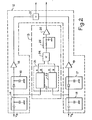
- This device 8 is shown in FIG. 2. It comprises means 12 for detecting adaptation in module and means 13 for detecting adaptation in phase.
- the module adaptation detection means 12 are conventionally produced by means of two capacitive dividers 14 and 15, one of which receives the input voltage V E and the other the output voltage V S. The ratios of these two capacitive dividers are determined so that the output voltages V S1 and V E1 of these two dividers are equal when the input voltages V s and V E of these two dividers are in a ratio equal to the product of the slope of the tube by its desired anode load resistance.
- the module adaptation detection means also comprise a circuit for detecting equality between the voltages V E 1 and V S1 , produced for example as follows.
- the capacitive dividers 14 and 15 are followed respectively by filter rectifiers 16 and 17 which respectively give signals proportional to the peak value of the signals V S1 and V S2 , and of opposite signs.
- Each of the rectifier-filters 16 and 17 is followed by an amplifier (18 and 19) and the outputs of these two amplifiers 18 and 19 are connected to the input of an analog adder 20 which provides detection information on its output. adaptation in module.
- the means 13 for phase adaptation detection include means 21 for phase shifting by ⁇ the phase difference existing between the voltages V s and V E.
- the means 21 comprise for example a first and a second 90 ° phase shifter, 22 and 23, identical, each provided with an input connected to the output of one of the capacitive dividers 14 and 15.
- Each phase shifter is provided with two outputs referenced A and B, one of which (A) provides the signal present at the input of the phase shifter, phase shifted by a phase shift a (a may be any) and the other (B) provides the signal collected on output A phase shifted by 90 °.
- phase shifters are well known in the art and will not be described in more detail. These are, for example, 90 ° phase shifters of the all-purpose quadrupole type with R-C networks.
- the phase adaptation detection device also comprises an analog multiplier 24 provided with two inputs connected respectively to the output A of the phase shifter 22 and to the output B of the phase shifter 23, or to the output B of the phase shifter 22 and to the output A of the phase shifter 23.
- the means 13 for phase adaptation detection also comprise a circuit 25 for calculating an average value (in particular by HF filtering), provided with an input connected to the output of the multiplier 24 and with an output which provides the information of phase matching detection through an amplifier 26.
- a circuit 25 for calculating an average value in particular by HF filtering
- the device 13 for phase adaptation detection shown in FIG. 2 operates as follows.
- ⁇ E and ⁇ S be the respective phases of the input voltages V E and output V S.
- phase shifter 22 and 23 has the phase shift provided by identical phase shifters 22 and 23 between the signals collected on their outputs A and the signals present on their inputs.
Applications Claiming Priority (2)
| Application Number | Priority Date | Filing Date | Title |
|---|---|---|---|
| FR8122274A FR2517493A1 (fr) | 1981-11-27 | 1981-11-27 | Dispositif de detection d'impedance optimum de charge d'anode d'un emetteur a tube dans une chaine d'emission haute frequence |
| FR8122274 | 1981-11-27 |
Publications (2)
| Publication Number | Publication Date |
|---|---|
| EP0080922A1 true EP0080922A1 (de) | 1983-06-08 |
| EP0080922B1 EP0080922B1 (de) | 1985-04-17 |
Family
ID=9264445
Family Applications (1)
| Application Number | Title | Priority Date | Filing Date |
|---|---|---|---|
| EP82402115A Expired EP0080922B1 (de) | 1981-11-27 | 1982-11-19 | Einrichtung zur optimalen Ermittlung der Anoden-Ladungsimpedanz an einem Röhrensender |
Country Status (7)
| Country | Link |
|---|---|
| US (1) | US4476578A (de) |
| EP (1) | EP0080922B1 (de) |
| JP (1) | JPS5897925A (de) |
| CA (1) | CA1193320A (de) |
| DE (1) | DE3263166D1 (de) |
| DK (1) | DK524682A (de) |
| FR (1) | FR2517493A1 (de) |
Cited By (2)
| Publication number | Priority date | Publication date | Assignee | Title |
|---|---|---|---|---|
| EP0412568A2 (de) * | 1989-08-11 | 1991-02-13 | Applied Materials, Inc. | Anpassungsschaltung und Verfahren zu ihrer Verwendung |
| EP0551813A2 (de) * | 1992-01-13 | 1993-07-21 | NPBI Nederlands Produktielaboratorium voor Bloedtransfusieapparatuur en Infusievloeistoffen B.V. | Vorrichtung zum Schweissen medizinischer Kunststoffgegenstände |
Families Citing this family (38)
| Publication number | Priority date | Publication date | Assignee | Title |
|---|---|---|---|---|
| JPS6028316A (ja) * | 1983-07-26 | 1985-02-13 | Kokusai Electric Co Ltd | 自動追尾整合装置 |
| FR2590993B1 (fr) * | 1985-11-29 | 1988-04-29 | Thomson Cgr | Dispositif et procede de reglage d'une antenne radiofrequence d'un appareil de resonance magnetique nucleaire |
| DE69217147T2 (de) * | 1991-09-04 | 1997-06-05 | Nec Corp | Funksendeempfänger |
| US5874926A (en) * | 1996-03-11 | 1999-02-23 | Murata Mfg Co. Ltd | Matching circuit and antenna apparatus |
| US6348679B1 (en) * | 1998-03-17 | 2002-02-19 | Ameritherm, Inc. | RF active compositions for use in adhesion, bonding and coating |
| US6649888B2 (en) | 1999-09-23 | 2003-11-18 | Codaco, Inc. | Radio frequency (RF) heating system |
| US8744384B2 (en) | 2000-07-20 | 2014-06-03 | Blackberry Limited | Tunable microwave devices with auto-adjusting matching circuit |
| US8064188B2 (en) | 2000-07-20 | 2011-11-22 | Paratek Microwave, Inc. | Optimized thin film capacitors |
| US9406444B2 (en) | 2005-11-14 | 2016-08-02 | Blackberry Limited | Thin film capacitors |
| US7711337B2 (en) | 2006-01-14 | 2010-05-04 | Paratek Microwave, Inc. | Adaptive impedance matching module (AIMM) control architectures |
| US8299867B2 (en) | 2006-11-08 | 2012-10-30 | Research In Motion Rf, Inc. | Adaptive impedance matching module |
| US7714676B2 (en) | 2006-11-08 | 2010-05-11 | Paratek Microwave, Inc. | Adaptive impedance matching apparatus, system and method |
| US7535312B2 (en) | 2006-11-08 | 2009-05-19 | Paratek Microwave, Inc. | Adaptive impedance matching apparatus, system and method with improved dynamic range |
| US7917104B2 (en) | 2007-04-23 | 2011-03-29 | Paratek Microwave, Inc. | Techniques for improved adaptive impedance matching |
| US8213886B2 (en) | 2007-05-07 | 2012-07-03 | Paratek Microwave, Inc. | Hybrid techniques for antenna retuning utilizing transmit and receive power information |
| US7991363B2 (en) | 2007-11-14 | 2011-08-02 | Paratek Microwave, Inc. | Tuning matching circuits for transmitter and receiver bands as a function of transmitter metrics |
| US8072285B2 (en) | 2008-09-24 | 2011-12-06 | Paratek Microwave, Inc. | Methods for tuning an adaptive impedance matching network with a look-up table |
| US8472888B2 (en) | 2009-08-25 | 2013-06-25 | Research In Motion Rf, Inc. | Method and apparatus for calibrating a communication device |
| US9026062B2 (en) | 2009-10-10 | 2015-05-05 | Blackberry Limited | Method and apparatus for managing operations of a communication device |
| US8803631B2 (en) | 2010-03-22 | 2014-08-12 | Blackberry Limited | Method and apparatus for adapting a variable impedance network |
| WO2011133657A2 (en) | 2010-04-20 | 2011-10-27 | Paratek Microwave, Inc. | Method and apparatus for managing interference in a communication device |
| US9379454B2 (en) | 2010-11-08 | 2016-06-28 | Blackberry Limited | Method and apparatus for tuning antennas in a communication device |
| US8712340B2 (en) | 2011-02-18 | 2014-04-29 | Blackberry Limited | Method and apparatus for radio antenna frequency tuning |
| US8655286B2 (en) | 2011-02-25 | 2014-02-18 | Blackberry Limited | Method and apparatus for tuning a communication device |
| US8626083B2 (en) | 2011-05-16 | 2014-01-07 | Blackberry Limited | Method and apparatus for tuning a communication device |
| US8594584B2 (en) | 2011-05-16 | 2013-11-26 | Blackberry Limited | Method and apparatus for tuning a communication device |
| US9769826B2 (en) | 2011-08-05 | 2017-09-19 | Blackberry Limited | Method and apparatus for band tuning in a communication device |
| US8948889B2 (en) | 2012-06-01 | 2015-02-03 | Blackberry Limited | Methods and apparatus for tuning circuit components of a communication device |
| US9853363B2 (en) | 2012-07-06 | 2017-12-26 | Blackberry Limited | Methods and apparatus to control mutual coupling between antennas |
| US9246223B2 (en) | 2012-07-17 | 2016-01-26 | Blackberry Limited | Antenna tuning for multiband operation |
| US9350405B2 (en) | 2012-07-19 | 2016-05-24 | Blackberry Limited | Method and apparatus for antenna tuning and power consumption management in a communication device |
| US9413066B2 (en) | 2012-07-19 | 2016-08-09 | Blackberry Limited | Method and apparatus for beam forming and antenna tuning in a communication device |
| US9362891B2 (en) | 2012-07-26 | 2016-06-07 | Blackberry Limited | Methods and apparatus for tuning a communication device |
| US10404295B2 (en) | 2012-12-21 | 2019-09-03 | Blackberry Limited | Method and apparatus for adjusting the timing of radio antenna tuning |
| US9374113B2 (en) | 2012-12-21 | 2016-06-21 | Blackberry Limited | Method and apparatus for adjusting the timing of radio antenna tuning |
| US9438319B2 (en) | 2014-12-16 | 2016-09-06 | Blackberry Limited | Method and apparatus for antenna selection |
| TWI587598B (zh) * | 2015-09-19 | 2017-06-11 | 立錡科技股份有限公司 | 諧振式無線電源發送電路及其控制方法 |
| CN112763806A (zh) * | 2021-03-03 | 2021-05-07 | 贵州电网有限责任公司 | 考虑移相变压器接入输电线路距离保护测量阻抗计算方法 |
Citations (5)
| Publication number | Priority date | Publication date | Assignee | Title |
|---|---|---|---|---|
| GB568053A (en) * | 1942-07-10 | 1945-03-15 | Patelhold Patentverwertung | An arrangement for automatically influencing the tuning of oscillation circuits |
| US3271684A (en) * | 1961-08-30 | 1966-09-06 | Siemens Ag | Method of automatically adjusting a broadcast transmitter |
| US3355667A (en) * | 1965-12-16 | 1967-11-28 | Collins Radio Co | Automatically tuned coupled resonant circuits |
| DE2342482A1 (de) * | 1972-09-08 | 1974-03-14 | Koepenick Funkwerk Veb | 90 grad-phasenbruecke |
| DE2923277A1 (de) * | 1979-06-08 | 1980-12-11 | Rohde & Schwarz | Anordnung zum selbsttaetigen abstimmen eines transformationsnetzwerkes |
Family Cites Families (3)
| Publication number | Priority date | Publication date | Assignee | Title |
|---|---|---|---|---|
| US3786355A (en) * | 1971-12-28 | 1974-01-15 | Cincinnati Electronics Corp | Radio frequency resistance discriminator having dead zone output characteristic |
| US3794941A (en) * | 1972-05-08 | 1974-02-26 | Hughes Aircraft Co | Automatic antenna impedance tuner including digital control circuits |
| CH621218A5 (de) * | 1977-06-22 | 1981-01-15 | Patelhold Patentverwertung |
-
1981
- 1981-11-27 FR FR8122274A patent/FR2517493A1/fr active Granted
-
1982
- 1982-11-19 EP EP82402115A patent/EP0080922B1/de not_active Expired
- 1982-11-19 JP JP57202250A patent/JPS5897925A/ja active Pending
- 1982-11-19 DE DE8282402115T patent/DE3263166D1/de not_active Expired
- 1982-11-22 US US06/443,635 patent/US4476578A/en not_active Expired - Fee Related
- 1982-11-24 CA CA000416271A patent/CA1193320A/en not_active Expired
- 1982-11-25 DK DK524682A patent/DK524682A/da not_active Application Discontinuation
Patent Citations (5)
| Publication number | Priority date | Publication date | Assignee | Title |
|---|---|---|---|---|
| GB568053A (en) * | 1942-07-10 | 1945-03-15 | Patelhold Patentverwertung | An arrangement for automatically influencing the tuning of oscillation circuits |
| US3271684A (en) * | 1961-08-30 | 1966-09-06 | Siemens Ag | Method of automatically adjusting a broadcast transmitter |
| US3355667A (en) * | 1965-12-16 | 1967-11-28 | Collins Radio Co | Automatically tuned coupled resonant circuits |
| DE2342482A1 (de) * | 1972-09-08 | 1974-03-14 | Koepenick Funkwerk Veb | 90 grad-phasenbruecke |
| DE2923277A1 (de) * | 1979-06-08 | 1980-12-11 | Rohde & Schwarz | Anordnung zum selbsttaetigen abstimmen eines transformationsnetzwerkes |
Cited By (4)
| Publication number | Priority date | Publication date | Assignee | Title |
|---|---|---|---|---|
| EP0412568A2 (de) * | 1989-08-11 | 1991-02-13 | Applied Materials, Inc. | Anpassungsschaltung und Verfahren zu ihrer Verwendung |
| EP0412568A3 (en) * | 1989-08-11 | 1991-07-17 | Applied Materials, Inc. | Matching network and method for using same |
| EP0551813A2 (de) * | 1992-01-13 | 1993-07-21 | NPBI Nederlands Produktielaboratorium voor Bloedtransfusieapparatuur en Infusievloeistoffen B.V. | Vorrichtung zum Schweissen medizinischer Kunststoffgegenstände |
| EP0551813A3 (en) * | 1992-01-13 | 1993-09-08 | Npbi Nederlands Produktielaboratorium Voor Bloedtransfusieapparatuur En Infusievloeistoffen B.V. | Apparatus for sealing medical plastic articles |
Also Published As
| Publication number | Publication date |
|---|---|
| DK524682A (da) | 1983-05-28 |
| CA1193320A (en) | 1985-09-10 |
| EP0080922B1 (de) | 1985-04-17 |
| JPS5897925A (ja) | 1983-06-10 |
| DE3263166D1 (en) | 1985-05-23 |
| US4476578A (en) | 1984-10-09 |
| FR2517493B1 (de) | 1984-03-02 |
| FR2517493A1 (fr) | 1983-06-03 |
Similar Documents
| Publication | Publication Date | Title |
|---|---|---|
| EP0080922B1 (de) | Einrichtung zur optimalen Ermittlung der Anoden-Ladungsimpedanz an einem Röhrensender | |
| EP2037576B1 (de) | Verfahren zur automatischen Impedanzanpassung einer Radiofrequenzschaltung und einer Funksender- oder -empfangskette mit automatischer Anpassung | |
| EP2476209B1 (de) | Impedanzabgleichsverfahren für eine mehrfrequenzantennne und übertragungs- oder empfangskanal mit automatischem abgleich | |
| EP2509222B1 (de) | Funkemissions- oder Empfangskette mit automatischer Impedanzanpassung, und entsprechendes Verfahren | |
| FR3028691B1 (fr) | Procede et module d'adaptation automatique d'impedance, en particulier pour une chaine d'emission ou reception radiofrequence | |
| FR2999044A1 (fr) | Dispositif radiofrequence avec compensation de dispersion de permittivite du substrat et procede de reglage | |
| EP3182588B1 (de) | Automatische anpassung der impedanz eines funkempfängers | |
| EP2357798A1 (de) | Verfahren und Vorrichtung zur Ansteuerung eines Bildsensors mit hohem Dynamikumfang | |
| EP0573321B1 (de) | Verfahren und Einrichtung zur automatischen Kompensation der Nichtlinearität der Modulationsgeraden für Radar mit Frequenzmodulation | |
| EP0463964B1 (de) | Anlage zur Erzeugung und zum Empfang von Ultraschall | |
| EP2978127B1 (de) | Verfahren zur digitalen kompensation von variationen, abhängig von der temperatur, einer elektrischen grösse einer integrierten weltraum-funktelekommunikationsausrüstung | |
| EP0350363B1 (de) | Verfahren und Anordnung zum Bestimmen der Entladungsimpedanz in einem Plasmareaktor | |
| FR2784179A1 (fr) | Chaine de mesure capacitive | |
| EP0473731B1 (de) | Verfahren und anordnung zum vergleich zweier veraenderlicher analogsignale | |
| FR3067475A1 (fr) | Procede et dispositif d'estimation d'un angle d'arrivee d'un signal radioelectrique incident | |
| EP1125411A1 (de) | Verfahren und system zur niveauregelung der störspektrallinien von dem frequenzspektrum des ausgangs einer einseitenband-frequenzumsetzungsanordnung | |
| FR2560998A1 (fr) | Procede de mesure d'impedance en haute frequence et installation de mesure d'impedance en haute frequence pour la mise en oeuvre de ce procede | |
| EP0080410A1 (de) | Bestimmungs- und Nachlaufanordnung für die Augenblickswerte des Extremums einer Funktion y = f(x), die für ein System mit einem Eingang x und einem Ausgang y charakteristik ist | |
| EP3913812A1 (de) | Impedanzanpassung | |
| EP0016674B1 (de) | Frequenzdiskriminator und damit stabilisierter Oszillator | |
| FR2715869A1 (fr) | Installation industrielle haute-fréquence, pour le traitement de matériaux, équipée de double mélangeurs équilibrés. | |
| EP2009790A1 (de) | Abstimmungsmethode der Resonanzfrequenz einer Antenne | |
| FR3084548A1 (fr) | Chaine de reception et/ou d'emission a radiofrequence et procede associe | |
| WO2020007975A1 (fr) | Système de détermination d'au moins une donnée correspondant à une mesure d'une caractéristique d'un médium | |
| FR2543305A1 (fr) | Dispositif de mesure d'intermodulation produite par un circuit haute frequence non lineaire |
Legal Events
| Date | Code | Title | Description |
|---|---|---|---|
| PUAI | Public reference made under article 153(3) epc to a published international application that has entered the european phase |
Free format text: ORIGINAL CODE: 0009012 |
|
| AK | Designated contracting states |
Designated state(s): CH DE GB IT LI NL |
|
| 17P | Request for examination filed |
Effective date: 19831110 |
|
| RBV | Designated contracting states (corrected) |
Designated state(s): DE GB |
|
| GRAA | (expected) grant |
Free format text: ORIGINAL CODE: 0009210 |
|
| AK | Designated contracting states |
Designated state(s): DE GB |
|
| REF | Corresponds to: |
Ref document number: 3263166 Country of ref document: DE Date of ref document: 19850523 |
|
| PLBE | No opposition filed within time limit |
Free format text: ORIGINAL CODE: 0009261 |
|
| STAA | Information on the status of an ep patent application or granted ep patent |
Free format text: STATUS: NO OPPOSITION FILED WITHIN TIME LIMIT |
|
| 26N | No opposition filed | ||
| PG25 | Lapsed in a contracting state [announced via postgrant information from national office to epo] |
Ref country code: GB Effective date: 19881119 |
|
| GBPC | Gb: european patent ceased through non-payment of renewal fee | ||
| PG25 | Lapsed in a contracting state [announced via postgrant information from national office to epo] |
Ref country code: DE Effective date: 19890801 |