EP0080731B2 - Semiconductor device comprising a buried oxide isolation - Google Patents
Semiconductor device comprising a buried oxide isolation Download PDFInfo
- Publication number
- EP0080731B2 EP0080731B2 EP82111034A EP82111034A EP0080731B2 EP 0080731 B2 EP0080731 B2 EP 0080731B2 EP 82111034 A EP82111034 A EP 82111034A EP 82111034 A EP82111034 A EP 82111034A EP 0080731 B2 EP0080731 B2 EP 0080731B2
- Authority
- EP
- European Patent Office
- Prior art keywords
- insulating film
- semiconductor device
- angle
- recesses
- channel width
- Prior art date
- Legal status (The legal status is an assumption and is not a legal conclusion. Google has not performed a legal analysis and makes no representation as to the accuracy of the status listed.)
- Expired - Lifetime
Links
Images




Classifications
-
- H—ELECTRICITY
- H10—SEMICONDUCTOR DEVICES; ELECTRIC SOLID-STATE DEVICES NOT OTHERWISE PROVIDED FOR
- H10D—INORGANIC ELECTRIC SEMICONDUCTOR DEVICES
- H10D62/00—Semiconductor bodies, or regions thereof, of devices having potential barriers
- H10D62/10—Shapes, relative sizes or dispositions of the regions of the semiconductor bodies; Shapes of the semiconductor bodies
- H10D62/13—Semiconductor regions connected to electrodes carrying current to be rectified, amplified or switched, e.g. source or drain regions
- H10D62/149—Source or drain regions of field-effect devices
- H10D62/151—Source or drain regions of field-effect devices of IGFETs
-
- H—ELECTRICITY
- H10—SEMICONDUCTOR DEVICES; ELECTRIC SOLID-STATE DEVICES NOT OTHERWISE PROVIDED FOR
- H10W—GENERIC PACKAGES, INTERCONNECTIONS, CONNECTORS OR OTHER CONSTRUCTIONAL DETAILS OF DEVICES COVERED BY CLASS H10
- H10W10/00—Isolation regions in semiconductor bodies between components of integrated devices
-
- H—ELECTRICITY
- H10—SEMICONDUCTOR DEVICES; ELECTRIC SOLID-STATE DEVICES NOT OTHERWISE PROVIDED FOR
- H10W—GENERIC PACKAGES, INTERCONNECTIONS, CONNECTORS OR OTHER CONSTRUCTIONAL DETAILS OF DEVICES COVERED BY CLASS H10
- H10W10/00—Isolation regions in semiconductor bodies between components of integrated devices
- H10W10/01—Manufacture or treatment
-
- H—ELECTRICITY
- H10—SEMICONDUCTOR DEVICES; ELECTRIC SOLID-STATE DEVICES NOT OTHERWISE PROVIDED FOR
- H10W—GENERIC PACKAGES, INTERCONNECTIONS, CONNECTORS OR OTHER CONSTRUCTIONAL DETAILS OF DEVICES COVERED BY CLASS H10
- H10W10/00—Isolation regions in semiconductor bodies between components of integrated devices
- H10W10/01—Manufacture or treatment
- H10W10/011—Manufacture or treatment of isolation regions comprising dielectric materials
- H10W10/012—Manufacture or treatment of isolation regions comprising dielectric materials using local oxidation of silicon [LOCOS]
- H10W10/0121—Manufacture or treatment of isolation regions comprising dielectric materials using local oxidation of silicon [LOCOS] in regions recessed from the surface, e.g. in trenches or grooves
- H10W10/0124—Manufacture or treatment of isolation regions comprising dielectric materials using local oxidation of silicon [LOCOS] in regions recessed from the surface, e.g. in trenches or grooves the regions having non-rectangular shapes, e.g. rounded
-
- H—ELECTRICITY
- H10—SEMICONDUCTOR DEVICES; ELECTRIC SOLID-STATE DEVICES NOT OTHERWISE PROVIDED FOR
- H10W—GENERIC PACKAGES, INTERCONNECTIONS, CONNECTORS OR OTHER CONSTRUCTIONAL DETAILS OF DEVICES COVERED BY CLASS H10
- H10W10/00—Isolation regions in semiconductor bodies between components of integrated devices
- H10W10/01—Manufacture or treatment
- H10W10/011—Manufacture or treatment of isolation regions comprising dielectric materials
- H10W10/012—Manufacture or treatment of isolation regions comprising dielectric materials using local oxidation of silicon [LOCOS]
- H10W10/0125—Manufacture or treatment of isolation regions comprising dielectric materials using local oxidation of silicon [LOCOS] comprising introducing electrical impurities in local oxidation regions, e.g. to alter LOCOS oxide growth characteristics
- H10W10/0126—Manufacture or treatment of isolation regions comprising dielectric materials using local oxidation of silicon [LOCOS] comprising introducing electrical impurities in local oxidation regions, e.g. to alter LOCOS oxide growth characteristics introducing electrical active impurities in local oxidation regions to create channel stoppers
-
- H—ELECTRICITY
- H10—SEMICONDUCTOR DEVICES; ELECTRIC SOLID-STATE DEVICES NOT OTHERWISE PROVIDED FOR
- H10W—GENERIC PACKAGES, INTERCONNECTIONS, CONNECTORS OR OTHER CONSTRUCTIONAL DETAILS OF DEVICES COVERED BY CLASS H10
- H10W10/00—Isolation regions in semiconductor bodies between components of integrated devices
- H10W10/10—Isolation regions comprising dielectric materials
- H10W10/13—Isolation regions comprising dielectric materials formed using local oxidation of silicon [LOCOS], e.g. sealed interface localised oxidation [SILO] or side-wall mask isolation [SWAMI]
Definitions
- This invention relates to a semiconductor device having an insulating film deposited in substrate recesses surrounding a transistor formation region.
- oxidized regions (called bird's beak) are formed in the lateral direction, resulting in a reduction of the VLSI packing density. That is, the gate oxide film is liable to have a greater thickness than the desired thickness due to the bird's beak. Because of this phenomena, the threshold voltage fluctuations are increased. In an extreme case, the thickness of the gate oxide film becomes substantially equal to the thickness of the field oxide film which results in an open circuit between the source and the drain.
- a BOX (buried oxide isolation) process as shown in Fig. 1 has been proposed.
- This BOX process is disclosed, for instance, in "A New Buried-oxide Field Isolation for VLSI Devices", K. Kurosawa et al. 39-th Annual Device Research Conference, June 22-24, 1981, University of California, Santa Barbara.
- a silicon substrate 10 is preliminarily etched to form recesses, and an insulating film 12 is stacked in these recesses. With the deposition of the insulating film 12, the resultant wafer has a flat surface.
- a gate electrode 16 is formed with a gate insulating film 14 interposed therebetween.
- an ion implantation layer 18 is formed in a superficial portion of the substrate under the insulating film 12 for preventing an inversion layer from forming.
- This process does not employ a thermal oxidation step which takes a long time.
- the fluctuations of the threshold voltage can be reduced even if the effective channel width is reduced with reduction of the dimensions of the elements.
- Fig. 2 illustrates how the threshold voltage changes with the effective channel width Weff in devices whose insulating films 12 are 300 nm (3,000 A), 500 nm (5,000 A) and 700 nm (7,000 A) thick, whose substrates 10 have an impurity concentration N suB of 2 x 10 15 cm4, and whose gate insulating films 14 are 100 nm (1,000 A) thick.
- This characteristic i.e., reduction of the threshold voltage with reduction of the effective channel width, is an undesirable characteristic of the element.
- the semiconductor device comprises a silicon substrate having a transistor region, forming a channel of a field effect transistor; said channel having a channel width of 1 ⁇ m or less; and an insulating film filling up recesses formed in the part of said silicon substrate surrounding said transistor region, the sidewall of said transistor region located in said recesses forming an angle 0 with the imaginary extension of the top surface of said transistor region, characterized in that: the angle 8 is defined as : and ⁇ 1, where ⁇ , is the relative permittivity of the insulating film.
- the threshold voltage With the above construction, it is possible to prevent the reduction of the threshold voltage with a reduction of the channel width. Thus, the design of the semiconductor device can be facilitated. Further, if the shape of the recesses is varied due to fluctuations of the manufacturing conditions, the threshold voltage is subject to fewer fluctuations. Thus, it is possible to improve the yield of the semiconductor device.
- a silicon substrate 10 is selectively etched except for a region 20 where transistors are to be formed.
- the recesses are formed in the part of the semiconductor substrate surrounding the region 20.
- the region 20 is formed such that its side wall 22 and the imaginary extension of the top surface 24 define an angle ⁇ ( ⁇ 90°).
- angle ⁇ may be obtained by means of reactive ion etching using a mask having inclined edges on the region 20.
- various values of angle ⁇ may be obtained by etching the substrate with different concentrations of CF 3 + in CF 4 .
- An ion implantation layer 18 for preventing an inversion layer from forming is formed in a superficial portion of the etched regions of the semiconductor substrate 10.
- a field insulation film 12 is formed on the ion implantation layer 18 such that it is contiguous to the side walls 22 of the region 20.
- a gate electrode 16 is formed over the region 20 with a gate insulating film 14 with a thickness t ox of 100 nm (1,000 A) interposed therebetween.
- the gate insulating film 14 and field insulation film 12 may be formed such that their surfaces are flush with each other.
- the gate electrode 16 is preferably formed to have a greater width than the width of the top surface 14 of the region 20.
- Fig. 4 shows the dependency of the threshold voltage of the MOS transistor on the effective channel width Weff.
- the ordinate is normalized in terms of the threshold voltage of a MOS transistor having a large channel width. As is seen from Fig. 4, the threshold voltage changes as the effective channel width becomes lower than 1 ⁇ . It was also found that the threshold voltage is independent of the effective channel width when the angle 0 is approximately 76°.
- Fig. 5 shows like characteristics in a case where the relative permittivity ⁇ l , of the gate insulating film 14 and field insulation film 12 is 10.
- the threshold voltage changes considerably as the effective channel width becomes lower than 1 ⁇ m.
- An ideal characteristic can be obtained when the angle 0 is set to 51 °.
- Fig. 6 shows the variation ⁇ V T of the threshold voltage (i.e., the difference thereof from the threshold voltage of a transistor having a large channel width) plotted against the angle 8 in a case where the effective channel width Weff is 0.2 ⁇ m.
- Various curves are shown for different values of the relative permittivity ⁇ l .
- MOS transistors which are substantially free from dependence on the effective channel width can be obtained when the angle 0 is in a range between 63° and 85° with the relative permittivity ⁇ l of 3.9, when the angle e is in a range between 52° and 82.5° with the relative permittivity ⁇ l of 6.0, and when the angle ⁇ is less than 72.5° with the relative permittivity ⁇ l of 10.
- Fig. 7 shows ranges of the optimum values of the angle ⁇ with respect to various values of the relative permittivity ⁇ l .
- the relative permittivity of an insulator is always greater than unity, so that ⁇ l ⁇ 1 must be met.
- the angle ⁇ is too small, the dimension of the MOS transistor in the direction of the channel width is excessively increased to reduce the integration density. For this reason, ⁇ 50° has to be met.
- the allowance of variation ⁇ V T is ⁇ 30 mV.
- the allowance of ⁇ V T is ⁇ 10 mV.
- a semiconductor device which is free from any dependency on the effective channel width can be obtained by setting the relative permittivity ⁇ l and angle 0 to be contained in the area mentioned above.
- the field insulation film 12 is 500 nm (5,000 A). It may be 300 nm (3,000 A) to 700 nm (7,000 A) thick to achieve the same effect as in the embodiment described above.
- the thickness t oxF of the film 12 is selected according to the type of device. If the device is a CMOS device, the field insulating film 12 functions as an element isolation region and must therefore frequently be much thicker than 500 nm (5,000 A) to prevent a latch up phenomenon.
- the optimum angle ⁇ is 76°.
- the optimum angle ⁇ changes little if the gate insulating film 14 is made 50 nm (500 A) or if the silicon substrate 10 has a different impurity concentration N SUB .
- the angle ⁇ hardly changes if impurity ions are injected to the substrate 10 to form a channel stopper or if they are injected into the channel region to adjust the threshold voltage.
- a thermal oxide film 26 having a thickness such as not to substantially change the shape of the semiconductor substrate, for instance approximately 50 nm (500 A), may be formed in the recesses formed in the substrate, and the insulating film 12 may be deposited on the thermal oxide film 26.
- the invention is applicable not only to a semiconductor device of an enhancement type but also to a semiconductor device of a depletion type. Further, the invention is applicable to both N and P channel semiconductor devices.
Landscapes
- Insulated Gate Type Field-Effect Transistor (AREA)
- Element Separation (AREA)
- Local Oxidation Of Silicon (AREA)
Description
- This invention relates to a semiconductor device having an insulating film deposited in substrate recesses surrounding a transistor formation region.
- Hitherto, a coplanar process has been employed to isolate semiconductor elements. In this process, however, oxidized regions (called bird's beak) are formed in the lateral direction, resulting in a reduction of the VLSI packing density. That is, the gate oxide film is liable to have a greater thickness than the desired thickness due to the bird's beak. Because of this phenomena, the threshold voltage fluctuations are increased. In an extreme case, the thickness of the gate oxide film becomes substantially equal to the thickness of the field oxide film which results in an open circuit between the source and the drain.
- To overcome this drawback, a BOX (buried oxide isolation) process as shown in Fig. 1 has been proposed. This BOX process is disclosed, for instance, in "A New Buried-oxide Field Isolation for VLSI Devices", K. Kurosawa et al. 39-th Annual Device Research Conference, June 22-24, 1981, University of California, Santa Barbara. In this BOX process, a
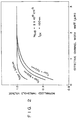
silicon substrate 10 is preliminarily etched to form recesses, and aninsulating film 12 is stacked in these recesses. With the deposition of theinsulating film 12, the resultant wafer has a flat surface. Over the portion of thesubstrate 10 surrounded by theinsulating film 12, agate electrode 16 is formed with agate insulating film 14 interposed therebetween. Usually, anion implantation layer 18 is formed in a superficial portion of the substrate under theinsulating film 12 for preventing an inversion layer from forming. This process does not employ a thermal oxidation step which takes a long time. Thus, the fluctuations of the threshold voltage can be reduced even if the effective channel width is reduced with reduction of the dimensions of the elements. - However, it has been confirmed by experiments and numerical calculations that, according to the BOX process, the threshold voltage is reduced with the reduction of the effective channel width. Fig. 2 illustrates how the threshold voltage changes with the effective channel width Weff in devices whose
insulating films 12 are 300 nm (3,000 A), 500 nm (5,000 A) and 700 nm (7,000 A) thick, whosesubstrates 10 have an impurity concentration NsuB of 2 x 1015 cm4, and whosegate insulating films 14 are 100 nm (1,000 A) thick. This characteristic, i.e., reduction of the threshold voltage with reduction of the effective channel width, is an undesirable characteristic of the element. Generally, it is desired that the threshold voltage be independent of the effective channel width. - It is accordingly the object of this invention to provide a semiconductor device including an insulating film deposited in substrate recesses surrounding a transistor formation region, in which the threshold voltage is independent of the effective channel width.
- To attain this object, the semiconductor device according to the invention comprises a silicon substrate having a transistor region, forming a channel of a field effect transistor; said channel having a channel width of 1µm or less; and an insulating film filling up recesses formed in the part of said silicon substrate surrounding said transistor region, the sidewall of said transistor region located in said recesses forming an angle 0 with the imaginary extension of the top surface of said transistor region, characterized in that: the angle 8 is defined as :


- With the above construction, it is possible to prevent the reduction of the threshold voltage with a reduction of the channel width. Thus, the design of the semiconductor device can be facilitated. Further, if the shape of the recesses is varied due to fluctuations of the manufacturing conditions, the threshold voltage is subject to fewer fluctuations. Thus, it is possible to improve the yield of the semiconductor device.
- The above and further objects and advantages of the invention will become more apparent from the following description taken in conjunction with the accompanying drawings, in which:
- Fig. 1 is a sectional view showing a prior art semiconductor device based on the BOX process;
- Fig. 2 is a graph showing the relation between the normalized threshold voltage and effective channel width Weffin a prior art semiconductor device;
- Fig. 3 is a sectional view showing a semiconductor device according to the present invention;
- Fig. 4 is a graph showing the relation between normalized threshold voltage and effective channel width Weff in a case where the relative permittivity of the insulating film is 3.9;
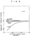
- Fig. 5 is a graph showing the relation between normalized threshold voltage and effective channel width Weff in a case where the relative permittivity of the insulating film is 10;
- Fig. 6 is a graph showing the relation between the variation AVT of the threshold voltage and the angle A in Fig. 3 in a case where the effective channel width Weff is 0.2 µ;
- Fig. 7 is a graph showing the permissible scope of relative permittivity εl, and angle 6 in the semiconductor device according to the present invention; and
- Fig. 8 is a sectional view showing a different embodiment of the semiconductor device according to the present invention.
- One embodiment of the semiconductor device according to the invention will now be described with reference to Fig. 3. In the BOX process, a
silicon substrate 10 is selectively etched except for aregion 20 where transistors are to be formed. As a result the recesses are formed in the part of the semiconductor substrate surrounding theregion 20. Theregion 20 is formed such that itsside wall 22 and the imaginary extension of thetop surface 24 define an angle θ (θ≤90°). Such a structure may be obtained by means of reactive ion etching using a mask having inclined edges on theregion 20. Alternatively, various values of angle θ may be obtained by etching the substrate with different concentrations of CF3+ in CF4. Anion implantation layer 18 for preventing an inversion layer from forming is formed in a superficial portion of the etched regions of thesemiconductor substrate 10. Afield insulation film 12 is formed on theion implantation layer 18 such that it is contiguous to theside walls 22 of theregion 20. Agate electrode 16 is formed over theregion 20 with agate insulating film 14 with a thickness tox of 100 nm (1,000 A) interposed therebetween. Preferably, thegate insulating film 14 andfield insulation film 12 may be formed such that their surfaces are flush with each other. Thegate electrode 16 is preferably formed to have a greater width than the width of thetop surface 14 of theregion 20. - Fig. 4 shows the dependency of the threshold voltage of the MOS transistor on the effective channel width Weff. The curves shown are obtained for various values of the angle 0 by setting the impurity concentration NSUB of the
silicon substrate 10 to 2x1015 cm-3, and the thickness of the field insulation film tOXF to 500 nm (5,000 A) and forming thegate insulating film 14 andfield insulation film 12 with silicon oxide having a relative permittivity of εl=3.9. The ordinate is normalized in terms of the threshold voltage of a MOS transistor having a large channel width. As is seen from Fig. 4, the threshold voltage changes as the effective channel width becomes lower than 1 µ. It was also found that the threshold voltage is independent of the effective channel width when the angle 0 is approximately 76°. - Fig. 5 shows like characteristics in a case where the relative permittivity εl, of the
gate insulating film 14 andfield insulation film 12 is 10. In this case again, the threshold voltage changes considerably as the effective channel width becomes lower than 1 µm. An ideal characteristic can be obtained when the angle 0 is set to 51 °. - Fig. 6 shows the variation ΔVT of the threshold voltage (i.e., the difference thereof from the threshold voltage of a transistor having a large channel width) plotted against the angle 8 in a case where the effective channel width Weff is 0.2 µm. Various curves are shown for different values of the relative permittivity εl. If the allowance of AVT is set to ±50 mV, MOS transistors which are substantially free from dependence on the effective channel width can be obtained when the angle 0 is in a range between 63° and 85° with the relative permittivity εl of 3.9, when the angle e is in a range between 52° and 82.5° with the relative permittivity εl of 6.0, and when the angle θ is less than 72.5° with the relative permittivity εl of 10.
- Fig. 7 shows ranges of the optimum values of the angle θ with respect to various values of the relative permittivity εl. The ranges are confined in an area defined by curve a, curve β, curve εl=1 and curve θ=50°. The relative permittivity of an insulator is always greater than unity, so that εl≥1 must be met. In addition, if the angle θ is too small, the dimension of the MOS transistor in the direction of the channel width is excessively increased to reduce the integration density. For this reason, θ≥50° has to be met. The curve a and β are given as θ = -0.2778
ε l3 + 0.2778εl 2-639εl + 88.39 (1) and θ = -0.009259εl3-0.2222εl2-2.528εl + 76.76 (2) Preferably, the allowance of variation ΔVT is ±30 mV. In this case, the curves a'and β' representing the upper and lower limits respectively, are given as θ = -0.2778εl2 + 1.056εl + 81.22 (3) and θ = -0.00959εl3-0.1389εl2-1.778εl + 78.93 (4) - More preferably, the allowance of ΔVT is ±10 mV. In this case, the curves a" and β" representing the upper and lower limits respectively, are given as θ = 0.0216εl3-0.5648s,2 + 1.037s, + 80.51 (5) and θ = 0.02778εl3-0.6944
ε l2= + 0.8889εl + 78.78 (6) A semiconductor device which is free from any dependency on the effective channel width can be obtained by setting the relative permittivity εl and angle 0 to be contained in the area mentioned above. In particular, it is possible to use a dielectric with a relative permittivity of 5.0 or above, for instance silicon nitride. - In the embodiment described above, the
field insulation film 12 is 500 nm (5,000 A). It may be 300 nm (3,000 A) to 700 nm (7,000 A) thick to achieve the same effect as in the embodiment described above. The thickness toxF of thefilm 12 is selected according to the type of device. If the device is a CMOS device, thefield insulating film 12 functions as an element isolation region and must therefore frequently be much thicker than 500 nm (5,000 A) to prevent a latch up phenomenon. - If the
field insulation film 12 and thegate insulating film 14 are made of silicon oxide having a relative permittivity εl of 3.9, the optimum angle θ is 76°. The optimum angle θ changes little if thegate insulating film 14 is made 50 nm (500 A) or if thesilicon substrate 10 has a different impurity concentration NSUB. In other words, the angle θ hardly changes if impurity ions are injected to thesubstrate 10 to form a channel stopper or if they are injected into the channel region to adjust the threshold voltage. - While in the above embodiment the insulating film has been deposited directly in the feld region, this is by no means limitative. For example, as shown in Fig. 8, a
thermal oxide film 26 having a thickness such as not to substantially change the shape of the semiconductor substrate, for instance approximately 50 nm (500 A), may be formed in the recesses formed in the substrate, and the insulatingfilm 12 may be deposited on thethermal oxide film 26. Further, the invention is applicable not only to a semiconductor device of an enhancement type but also to a semiconductor device of a depletion type. Further, the invention is applicable to both N and P channel semiconductor devices.
Claims (5)
characterized in that:
Applications Claiming Priority (2)
| Application Number | Priority Date | Filing Date | Title |
|---|---|---|---|
| JP190641/81 | 1981-11-30 | ||
| JP56190641A JPS5893250A (en) | 1981-11-30 | 1981-11-30 | Semiconductor device |
Publications (4)
| Publication Number | Publication Date |
|---|---|
| EP0080731A2 EP0080731A2 (en) | 1983-06-08 |
| EP0080731A3 EP0080731A3 (en) | 1986-05-07 |
| EP0080731B1 EP0080731B1 (en) | 1988-09-14 |
| EP0080731B2 true EP0080731B2 (en) | 1991-11-21 |
Family
ID=16261445
Family Applications (1)
| Application Number | Title | Priority Date | Filing Date |
|---|---|---|---|
| EP82111034A Expired - Lifetime EP0080731B2 (en) | 1981-11-30 | 1982-11-30 | Semiconductor device comprising a buried oxide isolation |
Country Status (3)
| Country | Link |
|---|---|
| EP (1) | EP0080731B2 (en) |
| JP (1) | JPS5893250A (en) |
| DE (1) | DE3279042D1 (en) |
Families Citing this family (2)
| Publication number | Priority date | Publication date | Assignee | Title |
|---|---|---|---|---|
| US5173438A (en) * | 1991-02-13 | 1992-12-22 | Micron Technology, Inc. | Method of performing a field implant subsequent to field oxide fabrication by utilizing selective tungsten deposition to produce encroachment-free isolation |
| US6097072A (en) * | 1996-03-28 | 2000-08-01 | Advanced Micro Devices | Trench isolation with suppressed parasitic edge transistors |
Family Cites Families (7)
| Publication number | Priority date | Publication date | Assignee | Title |
|---|---|---|---|---|
| NL131898C (en) * | 1965-03-26 | |||
| US3725160A (en) * | 1970-12-30 | 1973-04-03 | Texas Instruments Inc | High density integrated circuits |
| US3986200A (en) * | 1974-01-02 | 1976-10-12 | Signetics Corporation | Semiconductor structure and method |
| US4161039A (en) * | 1976-12-15 | 1979-07-10 | Siemens Aktiengesellschaft | N-Channel storage FET |
| US4187125A (en) * | 1976-12-27 | 1980-02-05 | Raytheon Company | Method for manufacturing semiconductor structures by anisotropic and isotropic etching |
| JPS55105373A (en) * | 1978-12-04 | 1980-08-12 | Mostek Corp | Metal oxide semiconductor transistor and method of fabricating same |
| EP0048175B1 (en) * | 1980-09-17 | 1986-04-23 | Hitachi, Ltd. | Semiconductor device and method of manufacturing the same |
-
1981
- 1981-11-30 JP JP56190641A patent/JPS5893250A/en active Pending
-
1982
- 1982-11-30 EP EP82111034A patent/EP0080731B2/en not_active Expired - Lifetime
- 1982-11-30 DE DE8282111034T patent/DE3279042D1/en not_active Expired
Also Published As
| Publication number | Publication date |
|---|---|
| JPS5893250A (en) | 1983-06-02 |
| EP0080731B1 (en) | 1988-09-14 |
| EP0080731A2 (en) | 1983-06-08 |
| DE3279042D1 (en) | 1988-10-20 |
| EP0080731A3 (en) | 1986-05-07 |
Similar Documents
| Publication | Publication Date | Title |
|---|---|---|
| KR0173111B1 (en) | Trench Gate MOS FET | |
| KR950001151B1 (en) | Manufacturing method of semiconductor device | |
| US5970338A (en) | Method of producing an EEPROM semiconductor structure | |
| EP0059848A2 (en) | FET and method for manufacturing such | |
| US5773330A (en) | Semiconductor device and method for fabricating the same | |
| KR0170457B1 (en) | Method of manufacturing semiconductor device with mosfet | |
| US4229756A (en) | Ultra high speed complementary MOS device | |
| US6229184B1 (en) | Semiconductor device with a modulated gate oxide thickness | |
| US4906591A (en) | Method of manufacturing a semiconductor device having an electric contact portion | |
| US6656810B1 (en) | Semiconductor device capable of reducing dispersion in electrical characteristics and operating at high speed and method for fabricating the same | |
| US5145797A (en) | Method of making semiconductor devices having an implant damage protection film on the gate electrode sidewalls | |
| EP0080731B1 (en) | Semiconductor device comprising a buried oxide isolation | |
| US4228447A (en) | Submicron channel length MOS inverter with depletion-mode load transistor | |
| KR100233802B1 (en) | Semiconductor device and manufacturing method thereof | |
| KR100752194B1 (en) | Manufacturing Method of Semiconductor Device | |
| US8232608B2 (en) | Semiconductor device and method for manufacturing semiconductor device | |
| US4651411A (en) | Method of manufacturing a MOS device wherein an insulating film is deposited in a field region | |
| US5726082A (en) | Semiconductor device and method for fabricating the same | |
| US5518949A (en) | Electrical isolation method for devices made on SOI wafer | |
| US5691564A (en) | Semiconductor device with high speed operation and high integration | |
| JPH05343676A (en) | Field-effect transistor and manufacturing method thereof | |
| US6184090B1 (en) | Fabrication method for a vertical MOS transistor | |
| JP2793141B2 (en) | Method of manufacturing semiconductor device having trench element isolation film | |
| JPH1187697A (en) | Semiconductor manufacturing method, semiconductor memory device manufacturing method, and semiconductor device | |
| KR0126789B1 (en) | Fabrication method of mosfet |
Legal Events
| Date | Code | Title | Description |
|---|---|---|---|
| PUAI | Public reference made under article 153(3) epc to a published international application that has entered the european phase |
Free format text: ORIGINAL CODE: 0009012 |
|
| 17P | Request for examination filed |
Effective date: 19821130 |
|
| AK | Designated contracting states |
Designated state(s): DE FR GB IT |
|
| RAP1 | Party data changed (applicant data changed or rights of an application transferred) |
Owner name: KABUSHIKI KAISHA TOSHIBA |
|
| PUAL | Search report despatched |
Free format text: ORIGINAL CODE: 0009013 |
|
| AK | Designated contracting states |
Kind code of ref document: A3 Designated state(s): DE FR GB IT |
|
| 17Q | First examination report despatched |
Effective date: 19880118 |
|
| GRAA | (expected) grant |
Free format text: ORIGINAL CODE: 0009210 |
|
| AK | Designated contracting states |
Kind code of ref document: B1 Designated state(s): DE FR GB IT |
|
| ITF | It: translation for a ep patent filed | ||
| REF | Corresponds to: |
Ref document number: 3279042 Country of ref document: DE Date of ref document: 19881020 |
|
| ET | Fr: translation filed | ||
| PLBI | Opposition filed |
Free format text: ORIGINAL CODE: 0009260 |
|
| 26 | Opposition filed |
Opponent name: DEUTSCHE ITT INDUSTRIES GMBH, FREIBURG Effective date: 19890609 |
|
| PUAH | Patent maintained in amended form |
Free format text: ORIGINAL CODE: 0009272 |
|
| STAA | Information on the status of an ep patent application or granted ep patent |
Free format text: STATUS: PATENT MAINTAINED AS AMENDED |
|
| 27A | Patent maintained in amended form |
Effective date: 19911121 |
|
| AK | Designated contracting states |
Kind code of ref document: B2 Designated state(s): DE FR GB IT |
|
| ITTA | It: last paid annual fee | ||
| ITF | It: translation for a ep patent filed | ||
| ET3 | Fr: translation filed ** decision concerning opposition | ||
| PGFP | Annual fee paid to national office [announced via postgrant information from national office to epo] |
Ref country code: FR Payment date: 19961111 Year of fee payment: 15 |
|
| PGFP | Annual fee paid to national office [announced via postgrant information from national office to epo] |
Ref country code: GB Payment date: 19961121 Year of fee payment: 15 |
|
| PGFP | Annual fee paid to national office [announced via postgrant information from national office to epo] |
Ref country code: DE Payment date: 19961206 Year of fee payment: 15 |
|
| PG25 | Lapsed in a contracting state [announced via postgrant information from national office to epo] |
Ref country code: GB Free format text: LAPSE BECAUSE OF NON-PAYMENT OF DUE FEES Effective date: 19971130 Ref country code: FR Free format text: THE PATENT HAS BEEN ANNULLED BY A DECISION OF A NATIONAL AUTHORITY Effective date: 19971130 |
|
| GBPC | Gb: european patent ceased through non-payment of renewal fee |
Effective date: 19971130 |
|
| PG25 | Lapsed in a contracting state [announced via postgrant information from national office to epo] |
Ref country code: DE Free format text: LAPSE BECAUSE OF NON-PAYMENT OF DUE FEES Effective date: 19980801 |
|
| REG | Reference to a national code |
Ref country code: FR Ref legal event code: ST |