EP0078542B1 - Color video signal recording apparatus - Google Patents
Color video signal recording apparatus Download PDFInfo
- Publication number
- EP0078542B1 EP0078542B1 EP82110123A EP82110123A EP0078542B1 EP 0078542 B1 EP0078542 B1 EP 0078542B1 EP 82110123 A EP82110123 A EP 82110123A EP 82110123 A EP82110123 A EP 82110123A EP 0078542 B1 EP0078542 B1 EP 0078542B1
- Authority
- EP
- European Patent Office
- Prior art keywords
- frequency
- signal
- divider
- phase
- recording
- Prior art date
- Legal status (The legal status is an assumption and is not a legal conclusion. Google has not performed a legal analysis and makes no representation as to the accuracy of the status listed.)
- Expired
Links
Images


Classifications
-
- H—ELECTRICITY
- H04—ELECTRIC COMMUNICATION TECHNIQUE
- H04N—PICTORIAL COMMUNICATION, e.g. TELEVISION
- H04N9/00—Details of colour television systems
- H04N9/79—Processing of colour television signals in connection with recording
- H04N9/80—Transformation of the television signal for recording, e.g. modulation, frequency changing; Inverse transformation for playback
- H04N9/82—Transformation of the television signal for recording, e.g. modulation, frequency changing; Inverse transformation for playback the individual colour picture signal components being recorded simultaneously only
- H04N9/83—Transformation of the television signal for recording, e.g. modulation, frequency changing; Inverse transformation for playback the individual colour picture signal components being recorded simultaneously only the recorded chrominance signal occupying a frequency band under the frequency band of the recorded brightness signal
- H04N9/84—Transformation of the television signal for recording, e.g. modulation, frequency changing; Inverse transformation for playback the individual colour picture signal components being recorded simultaneously only the recorded chrominance signal occupying a frequency band under the frequency band of the recorded brightness signal the recorded signal showing a feature, which is different in adjacent track parts, e.g. different phase or frequency
Definitions
- the present invention relates to a color video signal recording apparatus as described in the precharacterizing part of claim 1 or 2 and as essentially known f.c from GB-A-2040135.
- the composite color television signal is separated into the luminance signal and the chrominance signal, and these signals are processed separately and recorded on the magnetic tape.
- the carrier signal of the luminance signal extracted from the composite color television signal is modulated so that it is transformed into the frequency modulation signal, and the color subcarrier frequency of the chrominance signal is converted into a low frequency in the lower frequency band. Then, both signals are mixed to form a frequency multiplex signal, and it is recorded on the video track of the magnetic tape.
- the video signal is recorded without providing a guard band between adjacent video tracks. This causes signals recorded on adjacent video tracks to mix with each other, creating a crosstalk component during the reproducing operation.
- two video heads having different azimuth angles are used alternately so as to eliminate the crosstalk component by utilization of the azimuth loss in the heads.
- the azimuth loss in the video head is effective for a signal with a higher frequency such as the luminance signal, whereas it has little effect for a low-frequency signal below 1 MHz, and therefore, the chrominance signal which has been stepped down to a low frequency band cannot be rid of a crosstalk by the azimuth loss.
- the crosstalk component of the chrominance signal is eliminated in reproduction by utilization of the vertical correlation in the video signal.
- chroma signal there have been known two systems of color signal transformation for eliminating the crosstalk of the chrominance signal (will be termed simply chroma signal hereinafter) during reproduction by utilization of the vertical correlation of the video signal.
- 4-phase shift system is applied to the chroma signal, in which the chroma signal is phase-shifted by 90° in every horizontal period (will be termed simply 1H hereinafter) and the phase shift direction is reversed for each field for recording.
- single-field 4-phase shift system is applied to the chroma signal, in which the chroma signal for one field is phase-shifted by 90° in every 1H and another field is recorded without the phase shift.
- single-field phase invert system is applied to the chroma signal, with the chroma signal of one field phase-reversed for every 1 H and another field is recorded without the phase shift.
- frequency interleave system is applied to the chroma signal, in which an offset of 1/4 of the horizontal frequency (will be termed simply f H hereinafter) is provided between fields when the chroma signal is recorded.
- control pulses are recorded on the control track of the magnetic tape when it is recorded, and it is retrieved in the playback operation so as to control the tape speed.
- This control track is located at the bottom edge of the magnetic tape along the longitudinal direction.
- Another object of the present invention is to provide a color video signal recording apparatus capable of producing the pilot signals without using a dedicated oscillator.
- Fig. 1 shows in block diagram the principal portions of the frequency converting circuit for the chroma signal used in the conventional household magnetic recording and reproducing apparatus.
- the chroma signal separated from the composite color television signal is supplied to input terminal 1.
- the chroma signal received by the input terminal 1 has the first frequency of f 1 , and it is fed to the second frequency converter 2.
- the second frequency converter 2 is supplied with a carrier signal having the second frequency f 2 though band-pass filter (BPF) 5, and the converter 2 operates to mix the chroma signal and the carrier signal to provide a chroma signal having a frequency of f 2 -f 1 and a chroma signal having a frequency of f 2 +f, for the following low-pass filter (LPF) 3.
- BPF band-pass filter
- the LPF 3 conducts only one of chroma signals having a lower frequency, i.e., f 2 -f,, and passes it as output frequency f 4 to output terminal 4.
- the chroma signal provided at the output terminal 4 is then mixed with the luminance signal, and the resultant signal is recorded on the magnetic tape.
- Voltage controlled oscillator (VCO) 10 provides the oscillation output for 1/8 frequency divider 9 and 1/N frequency divider 12, and the 1/N frequency divider 12 reduces the frequency of the oscillation output by 1/N and supplies the divided frequency signal to phase detector 11.
- the phase detector 11 compares the phase of the horizontal signal in the color television signal received at input terminal 13 with the phase of the output signal of the 1/N frequency divider 12, and controls the VCO 10 so as to lock the phase of the oscillation output of the VCO 10 to the phase of the horizontal signal.
- 1/8 frequency divider 9 reduces the frequency of the output signal of the VCO 10 by 1/8 so as to produce the third frequency f 3 and supplies it to phase shift circuit 8.
- the phase shift circuit 8 shifts the phase of the output signal from the 1/8 frequency divider 9 by 90° or 180° and supplies the output to the first frequency converter 6.
- Crystal oscillator 7 generates the signal having the same frequency f, as of the chroma signal received by the input terminal 1, and supplies the oscillation output to the first frequency converter 6.
- the first frequency converter 6 mixes the output signal of the oscillator 7 with the output signal of the phase shift circuit 8 to produce a carrier signal having a frequency of f 1 +f 3 and another carrier signal having a frequency of f,-f 3 , then supplies these carrier signals to the BPF 5.
- the second frequency converter 2 mixes the carrier signal having the second frequency f 2 with the chroma signal having the first frequency, to provide at its output terminal 4 the chroma signal having the fourth frequency f 4 which is the difference between the frequency f 2 of the carrier signal and the frequency f, of the chroma signal.
- the first system of frequency conversion for the chroma signal in the NTSC system color television signal will be described.
- the phase shift circuit 8 shifts the phase of the third frequency (f 3 ) signal by +90° in every horizontal scanning period for the first field and by -90° for the second field. Consequently, the third frequency f 3 becomes for the first field, and for the second field.
- the second frequency f 2 becomes and the recording chroma frequency f 4 becomes that satisfies the necessary conditions of the recording chroma frequency of NTSC system: "it must have the offset of 1/4 f H " and "it must have a frequency difference of an odd multiple of 1/2 f H between fields”.
- the frequency division factor of the 1/N divider 12 is 1/32.
- the phase shift circuit 8 does not carry out phase shift for the first field and shifts the phase of the .
- third frequency (f 3 ) signal by -90° in every horizontal scanning period for the second field. Consequently, the third frequency is for the first field, and for the second field.
- the second frequency f 2 becomes and the fourth frequency f 4 of the recording chroma signal becomes that satisfies the necessary conditions of the recording chroma frequency of CCIR system: "it must have the offset of 1/8 fH" and "it must have a frequency difference of an odd multiple of 1/4 f H between fields".
- the problem raised here is that the NTSC system needs a 1/320 divider, while the CCIR system needs a 1/321 divider for the 1/N frequency divider 12. Therefore, in designing a common integrated circuit for NTSC and CCIR systems in accordance with the first system, the division factor of the frequency divider 12 needs to be switched for 1/320 and 1/321. Since both factors are developed as and and have no common prime number.
- the frequency divider 12 receives a high frequency input of 5 MHz, and it needs high-speed flip-flops (FFs) for dividing the frequency.
- the 1/320 divider is arranged by a cascade connection of six 1/2 dividers and a 1/5 divider, and only the first-stage 1/2 divider needs two high-speed flip-flops.
- the 1/321 divider needs two high-speed flip-flops for only the first-stage 1/3 divider.
- a frequency divider operable for both 1/320 and 1/321 divisions by switching cannot separate the high-speed and low-speed divider sections, since numbers 320 and 321 have no common prime number, and therefore it must be arranged entirely using high-speed flip-flops. More than eight high-speed flip-flops are needed for providing a 1/320 divider and 1/321 divider.
- an input frequency is below 3 MHz, flip-flops of the I 2 L (Integrated Injection Logic) type can be employed, which saves the chip area and power consumption considerably when fabricated into an integrated circuit.
- an input frequency above 3 MHz needs flip-flops of the ECL (Emitter Coupled Logic) type or the like, resulting in an increased chip area and power consumption.
- ECL emitter Coupled Logic
- an ECL device needs a ten-fold of chip area and ten-fold of power consumption as much as those of an I 2 L device, and there is a big difference in needing only one high-speed flip-flop or more than eight.
- the frequency conversion for the chroma signal of the NTSC color television signal in accordance with the second system.
- the phase shift circuit 8 performs phase shift by +180° in every horizontal scanning period for the first field, and performs no phase shift for the second field. Consequently, the third frequency f 3 becomes for the first field, and for the second field. Accordingly, the second frequency f 2 becomes and the fourth frequency of the recording chroma signal becomes that satisfies the necessary conditions for the recording chroma frequency of NTSC system.
- the first frequency f 1 is chosen to be 4.43 MHz
- the phase shift circuit 8 does not provide phase shifting for both fields. Consequently, the third frequency becomes for the first field, and for the second field. Accordingly, the second frequency becomes and the fourth frequency of the recording chroma signal becomes that satisfies the necessary conditions for the recording chroma frequency in CCIR system.
- the NTSC system needs a 1/350 divider
- the CCIR system needs a 1/351 divider for the first field and a 1/353 divider for the second field for the 1/N frequency divider 12. Therefore, in designing a common integrated circuit for NTSC and CCIR systems in accordance with the second system, the division factor of the frequency divider 12 needs to be switched for 1/350, 1/351 and 1/353. Since these factors are developed as and and have no common prime number, the 1/N frequency divider 12 needs more than eight high-speed flip-flops by the same reason as mentioned previously, resulting in an increased chip size and power consumption.
- the division factor of the 1/8 divider 9 is halved so that it is reduced to a 1/4 frequency divider.
- the oscillation frequency of the VCO 10 can be as low as the half of the former case, with the 1/N divider 12 having a division factor half that of the former case.
- this arrangement is not proper for the case of recording the CCIR color television signal.
- the recording chroma signal In recording the CCIR color television signal, the recording chroma signal must have an offset frequency of an odd multiple of 1/8 f H , and it is not possible for the chroma signal to have that offset frequency when the VCO output is divided by 4. Accordingly, the frequency divider 9 must also be a 1/8 divider, and the oscillation frequency of the VCO 10 cannot be halved.
- the oscillator 7 for generating the carrier signal must be provided with separate crystals for NTSC and CCIR systems when it is used commonly for both systems.
- a crystal oscillator providing the same frequency as the color signal frequency f 1 is required in order to eliminate the jitter from the reproduced chroma signal, causing the chroma signal recording and reproducing circuit to become complicated when it is fabricated into an integrated circuit.
- Fig. 2 is a relative amplitude vs. frequency graph showing the frequency distribution of the recording chroma signal and the frequency-modulated luminance signal obtained by processing the CCIR color television signal in accordance with the first chroma signal transformation system.
- the locations indicated by the arrows 21 and 22 show the top level frequency of the sync signal (3.8 MHz) and the white peak level frequency (5.1 MHz) of the frequency-modulated luminance signal, while a portion indicated by 23 is the associated harmonic section.
- Fig. 3 shows the typical frequency response of the magnetic recording and reproducing apparatus, where the response curve 28 has the peak at around 1 MHz.
- Reference number 29 shows the sag of the amplitude characteristics against the lower side band of the recording chroma signal, indicating an attenuation of about 10 dB at 125 kHz relative to 625 kHz. This deteriorates the transient response of the chroma signal, resulting in a significant deterioration in the quality of the reproduced picture, as is known in the field of art.
- the prior art recording and reproducing system employs a compensation circuit to modify the frequency response, however, it is not enough to obtain a satisfactory result.
- Fig. 4 shows frequencies of the pilot signals, where the relative amplitude of separate four pilot signals fp i , fp z , fp 3 and fp 4 , which are generally needed, are plotted against the frequency. These frequencies are chosen outside the recording chroma signal band so as to prevent interference with the video signal, and set to around 100 kHz for the lowest one in consideration of the response of the recording and reproducing system shown in Fig. 3.
- the third pilot signal fp 3 9.5 f H
- the lower cutoff frequency f LOW of the recording chroma signal is 125 kHz in the prior art system as shown in Fig. 2
- pilot signals cause an interference with the recording chroma signal.
- the lower cut-off frequency of the recording chroma signal needs to be set to around 164 kHz. This causes the recording chroma signal to have the lower side band 26 of a maximum of 461 kHz, resulting in a further deterioration of the picture quality, making it extremely difficult to practice the system.
- the above-mentioned pilot signals must have each accurate frequency when considered to provide interchangeability of the tape, and this can be achieved by producing the pilot signals by dividing the output frequency of the VCO 10 shown in Fig. 1.
- the frequency divider 9 is assumed to be a 1/4 divider and the VCO 10 to provide a frequency of 160 f H
- approximate frequencies for the four pilot signals can be obtained by dividing the frequency of the VCO 10 by 1/24, 1/21, 1/17 and 1/15, respectively.
- Fig. 5 is a block diagram showing one embodiment of the color video signal recording apparatus according to the present invention.
- the arrangement includes an input terminal 1 for receiving the recording chroma signal connected to one of the fixed contacts of the first switch 32, and a reproduced chroma signal input terminal 31 for receiving the chroma signal separated from the color television signal recorded on the magnetic tape during the playback operation, the terminal 31 being connected to another fixed contact of the first switch 32.
- the moving contact of the switch 32 is connected to the input terminal of ACC (Automatic Chroma-Gain Control) circuit 33 which has the output terminal connected to one input terminal of the second frequency converter 2 and also to one fixed contact of the second switch 39.
- ACC Automatic Chroma-Gain Control
- Another input terminal of the second frequency converter 2 is connected to the output terminal of band-pass filter 5, and the output terminal of the frequency converter 2 is connected to the input terminals of low-pass filter 3 and band-pass filter 34.
- the low-pass filter 3 has its output terminal connected to the input terminal of the first color killer amplifier 36
- the band-pass filter 34 has its output terminal connected to the input terminal of comb line filter 35.
- the first color killer amplifier 36 has a control terminal connected to the output terminal of a low-pass filter 40 and an output terminal connected to the output terminal 4 of the recording chroma signal.
- the comb line filter 35 has its output terminal connected to another fixed contact of the second switch 39 and also to the input terminal of the second color killer amplifier 37.
- the second color killer amplifier 37 has a control terminal connected to the output terminal of the low-pass filter 40 and an output terminal connected to the output terminal 38 for the reproduced chroma signal.
- the moving contact of the second switch 39 is connected to one input terminal of phase shift circuit 44 and also to the first input terminal of a killer detector 42.
- the phase detector 44 has another input terminal connected to the output terminal of the first oscillator 43 and an output terminal connected through low-pass filter 45 to the moving contact of the third switch 46.
- the first oscillator 43 has its input terminal connected to one fixed contact of the third switch 46 and an output terminal connected to one input terminal of the first frequency converter 6 and also through 90° phase shift circuit 41 to the second input terminal of the killer detector 42.
- the killer detector 42 has the third input terminal connected to the input terminal 47 for the burst gate pulse and an output terminal connected to the input terminal of the low-pass filter 40 and also through the first input terminal 50 of lower carrier generator 48 to the first input terminal of phase selection circuit 8.
- the second oscillator 10 is of a voltage controlled oscillator having its input terminal connected to the output terminal of horizontal AFC circuit 54 and an output terminal connected through the second input terminal 52 of the lower carrier generator 48 to the input terminal of the first frequency divider 9 and the input terminal of the second frequency divider 9.
- the horizontal AFC circuit 54 has its first input terminal connected through the second output terminal 51 of the circuit 48 to the output terminal of the second frequency divider 12, and the second input terminal connected to another fixed contact of the third switch 46, and further the third input terminal connected to the horizontal sync pulse input terminal 13.
- the phase selection circuit 8 has its input terminal connected to the output terminal of the first frequency divider 9, the third input terminal connected to the output terminal of the second frequency divider 12, and the fourth input terminal connected to the head pulse input terminal 49 of the circuit 48.
- the phase selection circuit 8 has its output terminal connected to another input terminal of the first frequency converter 6, the output terminal of which is connected to the input terminal of the band-pass filter 5.
- the first switch 32, second switch 39 and third switch 46 are positioned as shown in the figure, and the color signal with a carrier frequency of f, is supplied to the input terminal 1.
- the chroma signal is controlled by the ACC circuit 33 to have a constant amplitude, then conducted to the second frequency converter 2 and the second switch 39.
- the chroma signal fed to the second converter 2 is subjected to frequency conversion by the carrier signal f 2 supplied from the BPF 5, and the chroma signal reduced to the lower frequency f 4 is extracted at the output terminal of the LPF 3.
- the lower chroma signal is conducted through the color killer circuit 36 and sent out from the output terminal 4.
- the chroma signal fed to the second switch 39 is conducted to the phase detector 44 and the killer detector 42.
- the phase detector 44 detects the phase of the burst signal, and constitutes a phase-locked loop (PLL) circuit in conjunction with the LPF 45 and the first oscillator 43 so as to stabilize the oscillation frequency of the first oscillator 43.
- the killer detector 42 detects the burst signal for discriminating the color and monochrome signals and provides the discrimination signal for the first and second color killer circuits 36 and 37 through the LPF 40 so as to cut off the outputs of the color killer circuits 36 and 37 when processing a monochrome signal.
- the output signal of the second VCO 10 is reduced by the first frequency divider 9 to the carrier frequency f 4 of the lower chroma signal, and it is supplied to the phase selection circuit 8.
- the phase selection circuit 8 controls the phase of the recording chroma signal in every 1 H period in accordance with the head switching pulse supplied to the head pulse input terminal 49, i.e., providing a phase-lead or phase-lag by 90° in every 1H period for recording the first field, and recording the lower chroma signal without phase shifting for the second field.
- the shifted output signal from the phase selection circuit 8 is multiplied by the first converter 6 by the output signal of the first oscillator 43 which operates at a center frequency of f i , and the carrier signal f 2 having a frequency which is the sum of the given frequencies is obtained at-the output terminal of the BPF 5.
- the carrier signal f2 further multiplied by the second converter 2 by the color signal with the carrier frequency f" and the lower chroma signal with the carrier frequency f 4 is obtained as the difference of the given frequencies.
- the output signal from the second oscillator 10 is fed through the second frequency divider 12 to the horizontal AFC circuit 54 so that it is compared with the phase of the horizontal sync pulse separated from the input video signal at the input terminal 13 or the equivalent signal.
- the oscillator 10 constitutes a PLL for providing a frequency which is a multiple of the horizontal signal frequency in accordance with the division factor of the second frequency divider 12.
- the input terminal 31 receives the color signal retrieved from the magnetic tape, and this signal is subjected to phase-lead or phase-lag by 90° in every 1 H period for reproducing the first field, and is not shifted for reproducing the second field.
- the horizontal sync pulse input terminal 13 receives the horizontal sync pulse separated from the reproduced luminance signal or the equivalent signal, causing the second oscillator 10 to operate at the same frequency as in recording mode.
- the first frequency divider 9 and phase selection circuit 8 operate on the output of the oscillator 10 to have a phase-lead or phase-lag by 90° in each 1 H period for reproducing the first field, and provide no phase shifting for reproducing the second field, as in the case of recording mode, whereby the phase shift which has been made in the recording process can be compensated.
- the first oscillator 43 operates at f i in a free-run condition.
- the output of the first oscillator 43 is compared with the burst signal in the output signal from the second converter 2 by the phase detector 44, and the resultant output voltage is used to control the oscillation frequency of the second oscillator 10 through the horizontal AFC 54, so that the carrier frequency of the reproduced chroma signal is stabilized.
- the chroma signal with its phase and frequency restored to the original ones by the second converter 2 is supplied through the BPF 34 to the comb line filter 35 so that the crosstalk component caused by adjacent video tracks is eliminated from the chroma signal. Then the chroma signal without crosstalk component is delivered to the output terminal 38 through the second color killer amplifier 37 which is controlled by the killer detector 42.
- the color signal of NTSC system must have:
- the color signal of CCIR system must have:
- the color signal is phase-shifted by +90° in every horizontal scanning period for the first field, and by -90° for the second field, thereby providing an offset frequency of 1/2 f H between the first and second fields; or the color signal is phase-shifted by 180° in every horizontal scanning period for either the first or second field, thereby providing an offset frequency of 1/2 f H between the fields.
- the color signal is phase-shifted by 90° in every horizontal period for either the first or second field, thereby providing an offset frequency of 1/4 f H between the first and second fields.
- the color signal is phase-shifted by ⁇ 90° for each field, thereby providing an offset frequency of ⁇ 1/4 f H between the fields; or for the case of shifting the phase by 180° only for one of the fields, the frequency of the input signal to the phase shift circuit is chosen to be ⁇ n ⁇ 1/4(21-1) ⁇ f H (where n and I are constants), and an offset frequency which is an odd multiple of 1/4 f H can be achieved. It is also possible for CCIR system to have an offset frequency of 1/8 f H , by setting the frequency of the input signal to the phase shift circuit to, for example, (M-1/8)f H (where M is an integer).
- the chroma signal in NTSC system must have an offset frequency which is an odd multiple of 1/4 f H relative to the horizontal sync signal
- the chroma signal in CCIR system must have an offset frequency of 1/8 f H relative to the horizontal sync signal.
- the output frequency of the phase shift circuit may be set to (M ⁇ 1/8)f H
- the NTSC chroma signal can have an offset frequency which is an odd multiple of 1/4 f H by setting the output frequency of the phase shift circuit to (M ⁇ 2/8)f H .
- Such an offset frequency can be produced in the arrangement of Fig.
- the PLL oscillator 10 has within its loop the second frequency divider 12, which divides the oscillation frequency of the oscillator 10 by N and matches the phase of the output of the oscillator 10 to that of matches the phase of the output of the oscillator 10 to that of the horizontal sync signal. Then the oscillation frequency of the oscillator 10 has a relationship of N ⁇ f H .
- the phase selection circuit 8 For recording the CCIR chroma signal, the phase selection circuit 8 does not make a phase shift for the second field, but makes a +90° phase shift for the first field so as to provide a chroma frequency difference of f H /4 between the fields.
- the phase selection circuit 8 provides a +90° phase shift for the carrier signal in every horizontal scanning period for the first field, and provide a -90° phase shift in every horizontal scanning period for the second field, thereby realizing an offset frequency of ⁇ 1/4 f H and a chroma frequency difference of 1/2 f H between the fields. Therefore, the output frequency of the 1/8 frequency divider 9 must be a multiple of f H .
- the arrangement When the arrangement is realized by a common integrated circuit for both NTSC and CCIR systems, it will have a switch for the phase selection circuit 8 and a switch for the second frequency divider 12 to perform as a 1/120 divider and a 1/117 divider.
- the second frequency divider 12 as the 1/120 and 1/117 dividers will have an input frequency in the range of 1.8 to 1.9 MHz, and the divider for switching 1/120 and 1/117 can be arranged entirely using I 2 L devices, whereby the increased chip size and power consumption can be prevented.
- the frequency divider 12 can be arranged separately using two 1/3 dividers plus a 1/40 divider for NTSC system and a 1/39 divider for CCIR system. More specifically, the frequency divider 12 is arranged with the first 1/3 divider section made up of two high-speed flip-flops operating at 5.5 to 5.7 MHz, the second 1/3 divider made up of two medium-speed flip-flops operating at 1.8 to 1.9 MHz, and a divider made up of six or more low-speed flip-flops operating at 0.6 MHz for providing selectively the division factor of 1/39 and 1/40.
- the low-speed flip-flops can have a smaller chip size and lower power consumption as compared with medium-speed flip-flops.
- Fig. 6 an embodiment of the lower carrier generator used in the arrangement of Fig. 5.
- Fig. 6 components with the same reference numbers as those of Fig. 5 are the same as mentioned previously.
- the arrangement includes D-type flip-flops 100 through 107, an AND gate 108, NAND gates 109 through 116, and an inverter 117.
- the flip-flops 103-105 are enabled when the head pulse input terminal 49 is at 1's level in recording or reproducing a track of the first field for dividing output signal SH from the second frequency divider 12, i.e., the equivalent horizontal sync pulse, by 4, and provides signals 15g, 15h, 15i and 15j which become 1's level one by one sequentially in every 1H period. Then, one of the signals with the 90° phase difference from each other is selected by the NAND gates 109, 110, 111 and 112 in each 1 H period in the order of 15e, 15d, 15c and 15b, and outputted at the output of the NAND gate 113.
- the flip-flop 106 operates to adjust the time delay caused by the NAND gates 109-113.
- the flip-flop 107 makes a transition each time the phase correction signal input terminal 50 receives a 1's pulse so as to pass the signal at terminal Q of Q of the flip-flop 106 to the lower carrier output terminal 53.
- the flip-flops 103-105 are kept reset, providing the output 5g at 1's level, and the NAND gate 109 is enabled. Then, the lower carrier output terminal 53 provides the signal equivalent to the signai 15b so as to control the phase of the lower color signal as described previously.
- Fig. 7 shows the timing relationship of the principal signals shown in Fig. 6.
- Signal S vco is the output of the oscillator 10
- 15a is the output of the first flip-flop 100, i.e., the 1/2 divided waveform of the oscillator output.
- Signals 15b-15e are 1/4 divided waveforms of 15a from the first flip-flop 100, showing the phase difference by 90° from each other.
- SH is the signal equivalent t6 the horizontal sync pulse, and is supplied to the input terminal 51.
- Signal 1 5f is the head pulse supplied to the input terminal 49,15g is the output of the AND gate 108, 15h is the Q-output of the flip-flop 103, 15i is the Q-output of the flip-flop 104, and 15j is the Q-output of the flip-flop 105.
- Fig. 8 shows an embodiment of the second frequency divider 12 where components with the same reference numbers as shown in Fig. 5 are identical.
- the arrangement includes an input terminal 201 for receiving the output signal from the second oscillator 10, the third, fourth and fifth 1/3 frequency dividers, a 1/13 frequency divider, and an output terminal 206 for the frequency divided signal.
- the division factor of the second frequency divider 12 is determined from the division factors of the dividers 202-205, and in this case it is
- the fourth 1/3 frequency divider 203 receives the output of the third 1/3 divider 202, i.e., 1.8 MHz approximately, and it can be arranged using a medium-speed logic element.
- the fifth 1/3 divider 204 receives the output of the fourth 1/3 divider 203, i.e., 0.6 MHz approximately, and it can be arranged using a low-speed logic element as for the 1/13 frequency divider.
- Fig. 9 shows in detail an embodiment of the second frequency divider 12 shown in Fig. 8, where components with the same reference numbers as shown in Fig. 8 are identical.
- the arrangement includes flip-flops 300 through 312 and AND gates 313 through 316.
- the output signal S vco of the second oscillator 10 which generates the frequency fy co is received by terminal T of the flip-flops 300 and 301 constituting the third 1/3 frequency divider 202.
- a signal 8c having a frequency of f vco /3 is produced at terminal Q of the flip-flop 301 and it is fed to terminal T of the flip-flops 302 and 303 constituting the fourth 1/3 frequency divider 203.
- the flip-flop 303 produces at its Q terminal a signal 8f having a frequency of f vco /9, and it is conducted to terminal T of the flip-flops 304 and 305 constituting the fifth 1/3 frequency divider 204.
- the flip-flop 305 produces at its Q terminal a signal 8i having a frequency of f vcc/ 27, and it is conducted to terminal T of the flip-flops 306-312 constituting the 1/13 frequency divider 205. Finally, the flip-flop 312 produces at its Q terminal a signal 8q having a frequency of f vco /351 and delivers it to the divided signal output terminal 206.
- Fig. 10 is a timing chart for the principal signals shown in Fig. 9.
- S vco is the output signal of the second oscillator 10
- 8a-8c are the signal waveforms at the output of the AND gate 313 and terminal Q of the flip-flops 300 and 301, respectively
- 8d-8f are the signal waveforms at the output of the AND gate 314 and terminal Q of the flip-flops 302 and 303, respectively
- 8g-8i are the signal waveforms at the output of the AND gate 315 and terminal Q of the flip-flops 304 and 305, respectively.
- Signal 8i' is the same as signal 8i, but plotted on the contracted time scale, and it has a period of 27t relative to period t of S vco .
- Signals 8j-8q are the outputs of the AND gate 316 and the flip-flops 306-312 at their Q terminal.
- the lower carrier generator 48 may be arranged in general as shown in Fig. 11, where components with the same reference numbers as shown in Figs. 5 and 8 are identical.
- the arrangement of Fig. 11 includes a 1/m frequency divider 207 and a 1/1 frequency divider 208.
- the oscillation frequency of the second oscillator 10 can be expressed by the AFC circuit 54 as follows.
- the lower carrier frequency f 3 at the output terminal 53 for the CCIR chroma signal is In consideration of division factor 1/8 of the first frequency divider 9, the oscillation frequency f vco of the second oscillator 10 is Accordingly, from equations (7) and (8), m and I are given as The lower carrier frequency f 3 is determined by choosing the value of n and the polarity sign so that the value of I is a positive integer, with the value of m being 3, 5 or 7.
- the lower carrier frequency is generally determined as follows in order to reduce the beat interference by the lower chrominance signal to the luminance signal as in the case of the CCIR chroma signal. Accordingly, the oscillation frequency of the second oscillator 10 in Fig. 11 is adjusted so as to meet the equation (10), and this is achieved by switching the division factor of the frequency divider 12. However, in order to provide a simple arrangement for the frequency dividers, it is obvious that the relation similar to equation (9) needs to be established between the oscillation frequency of the oscillator 10 and the division factor of the frequency divider 12.
- the 1/m divider 207 in the frequency divider 12 preferably has a common division factor for the NTSC and CCIR signals. This condition is met by provision of a 1/3 divider for the 1/m frequency divider 207.
- the CCIR chroma signal can have an offset frequency which is an odd multiple of 1/8 f H by choosing the lower carrier frequency to be 3/8N f H (where N is an odd number).
- the recording chroma signal can have an offset frequency which is an odd multiple of 1/4 f H by choosing the lower carrier frequency to be 3/8N f H (where N is an integer), and at the same time, choosing the value of N so that N/4 is an integer for shifting the phase by 90°, or choosing the value of N so that (3N-2)/4 is an integer for shifting the phase by 180°.
- the value of N/4 becomes 30, an integer, and the condition for the case of 90° phase shift is met.
- Fig. 12 shows an embodiment of the lower carrier generator which is used commonly for the CCIR and NTSC signals, where components with the same reference numbers as shown in Fig. 11 are identical.
- the arrangement includes a 1/k frequency divider 209, switches 210 and 211, and a PAL/NTSC switching signal input terminal 212.
- the PAUNTSC switching signal at the input terminal 212 has a 1's level, providing the position of the switches 210 and 211 as shown in the figure, the division factor of the frequency divider 12 becomes and the oscillation frequency of the oscillator 10 becomes 351 f H .
- the input terminal 212 receives a 0's level, providing the position of the switches 210 and 211 oppositely to that of the figure, the division factor of the frequency divider 12 becomes and the oscillation frequency of the oscillator 10 becomes 378 f H . Accordingly, the lower carrier frequency f 3 becomes
- Fig. 13 shows another embodiment of the present invention, and this circuit is suitable for providing the pilot signals for recording the chroma signal of CCIR system.
- the output of the oscillator 10 is supplied to the frequency divider 9 which is made up of two frequency dividers 60 and 61.
- the former-stage divider 60 is a 1/2 frequency divider, and the latter-stage divider 61 is a 1/4 frequency divider.
- the output of the oscillator 10 is also supplied to 1/3 frequency divider 62, which provides the output for another frequency divider 63 which is made up of three 1/5 frequency dividers 64,65 and 66.
- the frequency dividers 62 and 63, the oscillator 10 and the phase detector 67 in combination constitute a PLL circuit.
- the output of the oscillator 10 is further supplied to the pilot signal generator 68, which has four frequency dividers, the first one being 1/58 divider, the second one 1/50 divider, the third one 1/40 divider, and the fourth one 1/36 divider.
- the output of the oscillator 10 is supplied commonly to the four frequency dividers in the pilot signal generator 68, and they perform frequency division and provide respective pilot signals fp 1 , f P2 , fp 3 and fp 4 at the output terminal 69.
- the output of the frequency divider 9 is connected to the phase selection circuit 8.
- the pilot signals must have frequencies satisfying the conditions given by equations (1) and (2).
- the first pilot signal frequency fp may be chosen to be 6.5 f H , the second one 7.5 f H , the third one 9.5 f H , and the fourth one 10.5 f H .
- the recording chroma frequency becomes (47-1/8)f H . Accordingly, the oscillation frequency of the oscillator 10 becomes 375f H .
- approximate pilot signal frequencies can be obtained by dividing the output frequency of the oscillator 10 by 1/58, 1/50, 1/40 and 1/36, respectively.
- the above frequency division factors of the pilot signals have a common term of 1/2, and thus by supplying the output of the 1/2 divider 60 in the frequency divider 9 to the pilot signal generator 68, the frequency dividers in it can have smaller division factors.
- Fig. 14 shows the frequency distribution of the above-mentioned pilot signals, the recording chroma signal and the frequency-modulated luminance signal.
- Fig. 15 is a block diagram showing another embodiment of the NTSC and CCIR chroma signal recording circuit.
- the frequency divider 12 is arranged to be for NTSC system, and for CCIR system.
- the 1/3 divider 62 is used commonly for the NTSC and CCIR signals
- the frequency divider 64 is operated selectively as a 1/6 divider for the NTSC signal and as a 1/5 divider for the CCIR signal
- the frequency divider 65 is switched for 1/3 and 1/5
- the frequency divider 66 is switched for 1/7 and 1/5 for the NTSC and CCIR signals, respectively.
- the frequency divider 9 is made up of a 1/2 divider 60 and a 1/4 divider 61.
- a waveform shaper 70 is connected between the phase selection circuit 8 and the frequency converter 6.
- the input terminal 75 receives the switching signal for selecting 90° phase shift or 180° phase shift for the phase selection circuit 8, and the terminal 76 receives the switching signal for selecting NTSC or CCIR mode.
- Reference number 77 denotes a burst gate circuit.
- the waveform shaper 70 serves to time the leading edge of the output signal from the phase selection circuit 8.
- One embodiment of the waveform shaper 70 is shown in Fig. 16, where the T terminal 72 of flip-flop 71 receives the output of the 1/2 frequency divider 60, while the D terminal 73 receives the output of the phase selection circuit 8, providing a correctly timed rising signal at the output terminal 74.
- N is set to 126 so that (3N-2)/4 is an integer, and the NTSC chroma signal is subjected to 180° phase shift.
- Fig. 17 shows an embodiment of the best-mode NTSC chroma signal recording circuit combined with the CCIR chroma signal recording circuit, wherein the pilot signals are provided.
- the arrangement of Fig. 17 includes a frequency divider 63 constituting a phase matching circuit, made up of a 1/3 frequency divider 65, a 1/6 divider 64 and a 1/7 divider 66, and it forms a 1/126 frequency divider effectively.
- the phase selection circuit 8 does not perform phase shifting for the first field and performs a 180° phase shift in every horizontal scanning period for the second field.
- the output frequency f 3 of the phase selection circuit 8 becomes for the second field. Consequently, the input frequency of the second converter 2 becomes and its output frequency becomes for the first field, and and for the second field.
- Fig. 18 shows an embodiment of the phase selection circuit 8.
- Figs. 19, 20 and 21 are timing charts for the arrangement of Fig. 18.
- the control signal input terminal 76 receives a high level signal so as to select the frequency division factor for the frequency divider 12 of and at the same time operates on NAND gates 168,169 and 170 through the terminal 181 so as to conduct the Q output of flip-flop 156 to the D input.
- Signal 14a at the terminal 49 indicating the track resets the flip-flops 156 and 157 during a high period. Then the flip-flops 156 and 157 provide the output signals as shown by the waveforms 14c, 14d, 14e and 14f in Fig. 20.
- the NAND gate 164 takes logical product in cooperation with inverter 125 between the signals 14b and 14e
- the NAND gate 165 and inverter 176 take logical product between the signals 14b and 14d
- the NAND gate 166 and inverter 177 take logical product between the signals 14c and 14d
- the NAND gate 167 and inverter 178 take logical product between the signals 14c and 14d, so as to provide respective output signals 14f, 14g, 14h and 14i.
- the VCO 10 provides the oscillation frequency of 378 f H in cooperation with the frequency divider 12 and the phase comparator 54.
- the output of the VCO 10 is conducted through the terminal 150 to terminal T of flip-flop 153 constituting a 1/2 frequency divider 60.
- the Q output of the flip-flop 153 is conducted to terminal T of flip-flop 154 constituting a 1/4 frequency divider 61. The same effect will result in this case when the Q output 13b of the flip-flop 153 is conducted to the T terminal of the flip-flops 154 and 155.
- These signals are taken logical product with the above-mentioned signals 14f, 14g, 14h and 14i by the NAND gates 160, 161, 162 and 163, respectively, and signals 13c and 13e with a phase difference of 180° are obtained alternately in every horizontal period at the output of the NAND gate 174 during a period when signal 14a indicating the track is low.
- the NAND gates 163,162 and 161 are disabled, allowing the NAND gate 174 to provide normally at its output the signal 13f.
- the NAND gates 171, 172 and 173 serve as switches controlled by the Q and Q outputs of the flip-flop 158, and the output signals at the Q and Q terminals of the NAND gate 174 are phase-reversed each time a pulse signal is applied to the terminal 151.
- the signal supplied to the.terminal151 is, for example, a signal representing the discontinuity of the reproduced chroma signal which occurs when the heads are switched.
- the phase of the output of the flip-flop 153 is regulated by the flip-flop 71 constituting a waveform shaper 70, then conducted through the terminal 152 to the frequency converter 6.
- CCIR mode differs from that of NTSC mode in that the frequency divider 12 is controlled by a low level signal at the control signal input terminal so as to select the frequency division factor of and the NAND gates 168, 169 and 170 are operated through the terminal 181 so as to conduct the Q output of the flip-flop 157 to the D input of the flip-flop 156.
- the outputs of the flip-flops 156 and 157 have the waveforms as shown by 14b, 14c, 14d and 14e in Fig. 15.
- the inverters 175, 176, 177 and 178 provide signals as shown by 14f, 14g, 14h and 14i in Fig. 21.
- the arrangement can readily be modified so that when the track indicating signal 14a is low, signals 13f, 13e, 13d and 13c are obtained in each horizontal period, and signal 13f is obtained normally when the signal 14a is high.
- the phase shift of both +90° and -90° can readily be realized.
- the recording chroma signal frequency is chosen to be 3/8 N ⁇ fH (where N is an odd number), whereby a large part of the lower carrier generator can be used for recording the chroma signal of NTSC system, and the chroma signals in the NTSC and CCIR color television signals can be processed by the common circuit.
- the recording chroma signal frequency is chosen to be 3/8 N . f H (where N is an integer), whereby color television signals in CCIR system can also be recorded by a slight modification of the circuit.
- N is chosen so that N/4 is an integer in case of 90° phase shift or N is chosen so that (3N-2)/4 is an integer in case of 180° phase shift for recording NTSC signals.
- N is chosen so that N/4 is an integer in case of 90° phase shift or N is chosen so that (3N-2)/4 is an integer in case of 180° phase shift for recording NTSC signals.
- Table 1 lists some preferable combinations of the color subcarrier frequencies for NTSC and CCIR systems.
- mode C, D, I, J, M, N, O and P are preferable since they are achieved by using frequency dividers each having a division factor of less than 10.
- mode M is preferable by the same reason. Accordingly, the best mode is M when merely considering the easiness of designing the chroma circuit.
- Table 2 lists some examples of the relationship between the color subcarrier frequency and the pilot signal frequencies which can be generated by the chroma circuit.
- I should be made as near zero as possible, and it should be 200 Hz (0.013 f H ) as the worst case.
- Suitable modes for generating the pilot signals are modes 6,11,13,16, and 20 for NTSC system, and modes 7, 10, 12, 15, 17, and 19 for CCIR system.
- the preferable combinations for NTSC and CCIR systems from the view point of generating the pilot signals are combinations of 6 and 7; 10 and 11; 12 and 13; 15 and 16; 16 and 17; and 19 and 20. All these combinations are further advantageous, providing a common division factor in producing the pilot signals for NTSC and CCIR systems.
- combinations 15 and 16, and 16 and 17 provide even frequency division factors for producing the pilot signals, allowing easy suppression against the generation of harmonic distortions in the pilot signals and also a simple arrangement of frequency dividers.
- the preferable modes in consideration of both the easiness of designing the chroma circuit and the easiness of producing the pilot signals are modes I, M and N when giving precedence to NTSC system, or mode M when giving precedence to CCIR system.
Landscapes
- Engineering & Computer Science (AREA)
- Multimedia (AREA)
- Signal Processing (AREA)
- Television Signal Processing For Recording (AREA)
- Processing Of Color Television Signals (AREA)
Description
- The present invention relates to a color video signal recording apparatus as described in the precharacterizing part of
claim - In the household magnetic recording and reproducing apparatus for recording a field of video signal aslant on the magnetic tape, the composite color television signal is separated into the luminance signal and the chrominance signal, and these signals are processed separately and recorded on the magnetic tape. In more detail, the carrier signal of the luminance signal extracted from the composite color television signal is modulated so that it is transformed into the frequency modulation signal, and the color subcarrier frequency of the chrominance signal is converted into a low frequency in the lower frequency band. Then, both signals are mixed to form a frequency multiplex signal, and it is recorded on the video track of the magnetic tape.
- In order for the household magnetic recording and reproducing apparatus to have a higher recording density on the magnetic tape, the video signal is recorded without providing a guard band between adjacent video tracks. This causes signals recorded on adjacent video tracks to mix with each other, creating a crosstalk component during the reproducing operation. On this account, two video heads having different azimuth angles are used alternately so as to eliminate the crosstalk component by utilization of the azimuth loss in the heads. However, the azimuth loss in the video head is effective for a signal with a higher frequency such as the luminance signal, whereas it has little effect for a low-frequency signal below 1 MHz, and therefore, the chrominance signal which has been stepped down to a low frequency band cannot be rid of a crosstalk by the azimuth loss. On this account, in general, the crosstalk component of the chrominance signal is eliminated in reproduction by utilization of the vertical correlation in the video signal.
- There have been known two systems of color signal transformation for eliminating the crosstalk of the chrominance signal (will be termed simply chroma signal hereinafter) during reproduction by utilization of the vertical correlation of the video signal. In one system for recording color television signals of NTSC system, 4-phase shift system is applied to the chroma signal, in which the chroma signal is phase-shifted by 90° in every horizontal period (will be termed simply 1H hereinafter) and the phase shift direction is reversed for each field for recording. In recording color television signals of CCIR system, single-field 4-phase shift system is applied to the chroma signal, in which the chroma signal for one field is phase-shifted by 90° in every 1H and another field is recorded without the phase shift.
- In the second system for recording color television signals of NTSC system, single-field phase invert system is applied to the chroma signal, with the chroma signal of one field phase-reversed for every 1 H and another field is recorded without the phase shift. In recording color television signals of CCIR system, frequency interleave system is applied to the chroma signal, in which an offset of 1/4 of the horizontal frequency (will be termed simply fH hereinafter) is provided between fields when the chroma signal is recorded.
- In these prior art technologies, however, the chroma signal is processed differently in NTSC system and CCIR system, resulting disadvantageously in the need for individual processing circuits. In addition, in order for the household magnetic recording and reproducing apparatus to playback at the same tape speed as in recording, control pulses are recorded on the control track of the magnetic tape when it is recorded, and it is retrieved in the playback operation so as to control the tape speed. This control track is located at the bottom edge of the magnetic tape along the longitudinal direction.
- Recently, an attempt for making the tape width more narrower has been made by eliminating the control track, thereby to provide more compact magnetic recording and reproducing apparatus. On this account, four pilot signals in place of the conventional control pulses are recorded on the video track on a multiplex basis with the video signal, and the four pilot signals are retrieved during the playback operation so as to control the playback tape speed. The four pilot signals are allocated in a frequency band lower than the band of the chroma signal. However, in the conventional household magnetic recording and reproducing apparatus, the lower side band of the chroma signal is located nearby the cutoff frequency of the video head response, preventing the pilot signals from being frequency-multiplexed simply, but necessitating the band of the chroma signal to be shifted to a higher frequency band.
- It is an object of the present invention to provide a color video signal recording apparatus capable of converting the frequency of the chroma signal in the color television signal of NTSC system and the chroma signal in the color television signal of CCIR system into lower frequencies by using a common circuit.
- This object is obtained according to the invention by a color video signal recording apparatus as defined in
claim 2. - Another object of the present invention is to provide a color video signal recording apparatus capable of producing the pilot signals without using a dedicated oscillator.
- The present invention will be apparent from the following detailed description taken in conjunction with the accompanying drawings, in which:
- Fig. 1 is a block diagram showing the chroma signal frequency converting circuit used in the conventional magnetic recording and reproducing apparatus;
- Fig. 2 is a frequency spectrum diagram for the recording signal in the conventional magnetic recording and reproducing apparatus;
- Fig. 3 is a frequency response diagram for the conventional magnetic recording and reproducing apparatus;
- Fig. 4 is a frequency spectrum diagram for the pilot signals;
- Fig. 5 is a block diagram showing the chroma signal frequency converting circuit in the color video signal recording apparatus embodying the present invention;
- Fig. 6 is a schematic diagram of the 1/8 frequency divider embodying the present invention;
- Fig. 7 is a set of waveform charts showing the operation of the circuit arrangement shown in Fig. 7;
- Fig. 8 is a block diagram exemplifying the 1/N frequency divider;
- Fig. 9 is a schematic diagram exemplifying the 1/N frequency divider;
- Fig. 10 is a set of waveform charts showing the operation of the circuit arrangement shown in Fig. 9;
- Fig. 11 is a block diagram showing another embodiment of the 1/N frequency divider;
- Fig. 12 is a block diagram of the 1/N frequency divider used in recording TV signals of NTSC system and CCIR system selectively;
- Fig. 13 is a block diagram showing another embodiment of the chroma signal frequency converting circuit for producing the pilot signals;
- Fig. 14 is a frequency spectrum diagram for the recording signal in the inventive color video signal recording apparatus;
- Fig. 15 is a block diagram showing another embodiment of the inventive chroma signal frequency converting circuit;
- Fig. 16 is a schematic diagram exemplifying the waveform shaping circuit used in the arrangement of Fig. 15;
- Fig. 17 is a block diagram showing still another embodiment of the inventive chroma signal frequency converting circuit;
- Fig. 18 is a schematic diagram exemplifying the phase selecting circuit; and
- Figs. 19, 20 and 21 are sets of waveform charts showing the operation of the circuit arrangement shown in Fig. 18.
- Before entering into the inventive color video signal recording apparatus, the arrangement of the chroma signal frequency converting circuit used in the conventional magnetic recording and reproducing apparatus and problems thereof will be described.
- Fig. 1 shows in block diagram the principal portions of the frequency converting circuit for the chroma signal used in the conventional household magnetic recording and reproducing apparatus. The chroma signal separated from the composite color television signal is supplied to
input terminal 1. The chroma signal received by theinput terminal 1 has the first frequency of f1, and it is fed to thesecond frequency converter 2. Thesecond frequency converter 2 is supplied with a carrier signal having the second frequency f2 though band-pass filter (BPF) 5, and theconverter 2 operates to mix the chroma signal and the carrier signal to provide a chroma signal having a frequency of f2-f1 and a chroma signal having a frequency of f2+f, for the following low-pass filter (LPF) 3. TheLPF 3 conducts only one of chroma signals having a lower frequency, i.e., f2-f,, and passes it as output frequency f4 tooutput terminal 4. The chroma signal provided at theoutput terminal 4 is then mixed with the luminance signal, and the resultant signal is recorded on the magnetic tape. Voltage controlled oscillator (VCO) 10 provides the oscillation output for 1/8frequency divider N frequency divider 12, and the 1/N frequency divider 12 reduces the frequency of the oscillation output by 1/N and supplies the divided frequency signal to phase detector 11. The phase detector 11 compares the phase of the horizontal signal in the color television signal received atinput terminal 13 with the phase of the output signal of the 1/N frequency divider 12, and controls theVCO 10 so as to lock the phase of the oscillation output of theVCO 10 to the phase of the horizontal signal. 1/8frequency divider 9 reduces the frequency of the output signal of theVCO 10 by 1/8 so as to produce the third frequency f3 and supplies it tophase shift circuit 8. Thephase shift circuit 8 shifts the phase of the output signal from the 1/8frequency divider 9 by 90° or 180° and supplies the output to thefirst frequency converter 6.Crystal oscillator 7 generates the signal having the same frequency f, as of the chroma signal received by theinput terminal 1, and supplies the oscillation output to thefirst frequency converter 6. Thefirst frequency converter 6 mixes the output signal of theoscillator 7 with the output signal of thephase shift circuit 8 to produce a carrier signal having a frequency of f1+f3 and another carrier signal having a frequency of f,-f3, then supplies these carrier signals to theBPF 5. TheBPF 5 conducts only one of the output signals from thefirst frequency converter 6 having a higher frequency, i.e., f, +f3, and supplies it as a carrier signal having the second frequency f2=f1+f3 to thesecond frequency converter 2. Then, as mentioned previously, thesecond frequency converter 2 mixes the carrier signal having the second frequency f2 with the chroma signal having the first frequency, to provide at itsoutput terminal 4 the chroma signal having the fourth frequency f4 which is the difference between the frequency f2 of the carrier signal and the frequency f, of the chroma signal. - The following will describe two methods of converting chroma signal frequency by the arrangement of Fig. 1 used in the conventional household magnetic recording and reproducing apparatus.
- First, the first system of frequency conversion for the chroma signal in the NTSC system color television signal will be described. In this case, the above-mentioned first frequency f, is chosen to be 3.58 MHz and the oscillation frequency N · fH of the
VCO 10 be 320x 15.7 kHz=5.04 MHz. The frequency division factor of the 1/N divider 12 is 1/N=1/320. Thephase shift circuit 8 shifts the phase of the third frequency (f3) signal by +90° in every horizontal scanning period for the first field and by -90° for the second field. Consequently, the third frequency f3 becomes

- Accordingly, the second frequency f2 becomes


- The following will describe the frequency conversion for the chroma signal in the CCIR color television signal performed by the first system. In this case, the first frequency is chosen to be f1=4.43 MHz and the oscillation frequency of the
VCO 10 is 321 x 15.6=5.02 MHz. The frequency division factor of the 1/N divider 12 is 1/32. Thephase shift circuit 8 does not carry out phase shift for the first field and shifts the phase of the . third frequency (f3) signal by -90° in every horizontal scanning period for the second field. Consequently, the third frequency is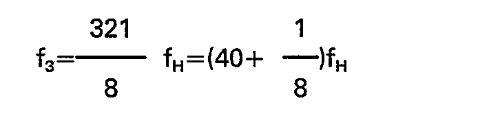

- Accordingly, the second frequency f2 becomes


N frequency divider 12. Therefore, in designing a common integrated circuit for NTSC and CCIR systems in accordance with the first system, the division factor of thefrequency divider 12 needs to be switched for 1/320 and 1/321. Since both factors are developed as

frequency divider 12 receives a high frequency input of 5 MHz, and it needs high-speed flip-flops (FFs) for dividing the frequency. The 1/320 divider is arranged by a cascade connection of six 1/2 dividers and a 1/5 divider, and only the first-stage 1/2 divider needs two high-speed flip-flops. Similarly, the 1/321 divider needs two high-speed flip-flops for only the first-stage 1/3 divider. However, a frequency divider operable for both 1/320 and 1/321 divisions by switching cannot separate the high-speed and low-speed divider sections, since numbers 320 and 321 have no common prime number, and therefore it must be arranged entirely using high-speed flip-flops. More than eight high-speed flip-flops are needed for providing a 1/320 divider and 1/321 divider. - If the input frequency is below 3 MHz, flip-flops of the I2L (Integrated Injection Logic) type can be employed, which saves the chip area and power consumption considerably when fabricated into an integrated circuit. On the other hand, an input frequency above 3 MHz needs flip-flops of the ECL (Emitter Coupled Logic) type or the like, resulting in an increased chip area and power consumption. Generally speaking, an ECL device needs a ten-fold of chip area and ten-fold of power consumption as much as those of an I2L device, and there is a big difference in needing only one high-speed flip-flop or more than eight.
- The following will describe the frequency conversion for the chroma signal of the NTSC color television signal in accordance with the second system. In this case, the above-mentioned first frequency fi is chosen to be 3.58 MHz and the oscillation frequency of the
VCO 10 be 350x15.7 kHz=5.5 MHz. The frequency division factor of the 1/N divider 12 is 1/N=1/350. Thephase shift circuit 8 performs phase shift by +180° in every horizontal scanning period for the first field, and performs no phase shift for the second field. Consequently, the third frequency f3 becomes


- The following will describe the frequency conversion for the chroma signal in the CCIR color television signal. In this case, the first frequency f1 is chosen to be 4.43 MHz, and the frequency division factor N of the 1/
N divider 12 varies for each field, N=351 for the first field and N=353 for the second field. Accordingly, the oscillation frequency of theVCO 10 becomes (352±1)x15.6 kHz and the 1/N frequency divider 12 has a factor of 1/N=1/(352±1). Thephase shift circuit 8 does not provide phase shifting for both fields. Consequently, the third frequency becomes


- The problem raised here is that the NTSC system needs a 1/350 divider, while the CCIR system needs a 1/351 divider for the first field and a 1/353 divider for the second field for the 1/
N frequency divider 12. Therefore, in designing a common integrated circuit for NTSC and CCIR systems in accordance with the second system, the division factor of thefrequency divider 12 needs to be switched for 1/350, 1/351 and 1/353. Since these factors are developed as


N frequency divider 12 needs more than eight high-speed flip-flops by the same reason as mentioned previously, resulting in an increased chip size and power consumption. - It can be considered that the division factor of the 1/8
divider 9 is halved so that it is reduced to a 1/4 frequency divider. In this case the oscillation frequency of theVCO 10 can be as low as the half of the former case, with the 1/N divider 12 having a division factor half that of the former case. However, this arrangement is not proper for the case of recording the CCIR color television signal. In recording the CCIR color television signal, the recording chroma signal must have an offset frequency of an odd multiple of 1/8 fH, and it is not possible for the chroma signal to have that offset frequency when the VCO output is divided by 4. Accordingly, thefrequency divider 9 must also be a 1/8 divider, and the oscillation frequency of theVCO 10 cannot be halved. - In addition, since the chroma signal in the NTSC color television signal and the chroma signal in the CCIR color television signal have each different frequency, the
oscillator 7 for generating the carrier signal must be provided with separate crystals for NTSC and CCIR systems when it is used commonly for both systems. - Moreover, a crystal oscillator providing the same frequency as the color signal frequency f1 is required in order to eliminate the jitter from the reproduced chroma signal, causing the chroma signal recording and reproducing circuit to become complicated when it is fabricated into an integrated circuit.
- Fig. 2 is a relative amplitude vs. frequency graph showing the frequency distribution of the recording chroma signal and the frequency-modulated luminance signal obtained by processing the CCIR color television signal in accordance with the first chroma signal transformation system. In the figure, the locations indicated by the
arrows - Fig. 3 shows the typical frequency response of the magnetic recording and reproducing apparatus, where the
response curve 28 has the peak at around 1 MHz. Reference number 29 shows the sag of the amplitude characteristics against the lower side band of the recording chroma signal, indicating an attenuation of about 10 dB at 125 kHz relative to 625 kHz. This deteriorates the transient response of the chroma signal, resulting in a significant deterioration in the quality of the reproduced picture, as is known in the field of art. On this account, the prior art recording and reproducing system employs a compensation circuit to modify the frequency response, however, it is not enough to obtain a satisfactory result. - Also there has been the prior art technology in which pilot signals are recorded on a multiplex basis with the video signal in order to enhance the tracking performance for the high density recording. Fig. 4 shows frequencies of the pilot signals, where the relative amplitude of separate four pilot signals fpi, fpz, fp3 and fp4, which are generally needed, are plotted against the frequency. These frequencies are chosen outside the recording chroma signal band so as to prevent interference with the video signal, and set to around 100 kHz for the lowest one in consideration of the response of the recording and reproducing system shown in Fig. 3. Specifically, in general, the first pilot signal is set to fpi =6.5 fH=102 kHz, the second pilot signal fp2=7.5 fH=117 kHz, the third pilot signal fp3=9.5 fH, and the fourth pilot signal fP4=10.5 fH=164 kHz. However, since the lower cutoff frequency fLOW of the recording chroma signal is 125 kHz in the prior art system as shown in Fig. 2, pilot signals cause an interference with the recording chroma signal. In addition, in order to provide a frequency separation between the pilot signals and the recording chroma signal, the lower cut-off frequency of the recording chroma signal needs to be set to around 164 kHz. This causes the recording chroma signal to have the
lower side band 26 of a maximum of 461 kHz, resulting in a further deterioration of the picture quality, making it extremely difficult to practice the system. - The above-mentioned pilot signals must have each accurate frequency when considered to provide interchangeability of the tape, and this can be achieved by producing the pilot signals by dividing the output frequency of the
VCO 10 shown in Fig. 1. In this case, when thefrequency divider 9 is assumed to be a 1/4 divider and theVCO 10 to provide a frequency of 160 fH, approximate frequencies for the four pilot signals can be obtained by dividing the frequency of theVCO 10 by 1/24, 1/21, 1/17 and 1/15, respectively. Thus the first pilot signal will have a frequency of fp,=160 fH/24=6.67 fH, the second pilot signal fp2=160 fH/21=7.62 fH, the third pilot signal fH=160 fH/17=9.41 fH, and the fourth pilot signal fH=160 fH/15=10.67 fH. - The conditions for the pilot signal frequencies are expressed by the following equations.


- The differences between (fp2-fp1) and (fp4-fp3), and between (fp3-fp1) and (fp4-fp2) are both 0.31 fH, that does not satisfy the conditions given by equations (1) and (2). Therefore, it is necessary to provide a stable oscillator, e.g., a crystal oscillator, in addition to the
VCO 10. - Fig. 5 is a block diagram showing one embodiment of the color video signal recording apparatus according to the present invention. The arrangement includes an
input terminal 1 for receiving the recording chroma signal connected to one of the fixed contacts of the first switch 32, and a reproduced chroma signal input terminal 31 for receiving the chroma signal separated from the color television signal recorded on the magnetic tape during the playback operation, the terminal 31 being connected to another fixed contact of the first switch 32. The moving contact of the switch 32 is connected to the input terminal of ACC (Automatic Chroma-Gain Control) circuit 33 which has the output terminal connected to one input terminal of thesecond frequency converter 2 and also to one fixed contact of thesecond switch 39. Another input terminal of thesecond frequency converter 2 is connected to the output terminal of band-pass filter 5, and the output terminal of thefrequency converter 2 is connected to the input terminals of low-pass filter 3 and band-pass filter 34. The low-pass filter 3 has its output terminal connected to the input terminal of the firstcolor killer amplifier 36, and the band-pass filter 34 has its output terminal connected to the input terminal ofcomb line filter 35. The firstcolor killer amplifier 36 has a control terminal connected to the output terminal of a low-pass filter 40 and an output terminal connected to theoutput terminal 4 of the recording chroma signal. Thecomb line filter 35 has its output terminal connected to another fixed contact of thesecond switch 39 and also to the input terminal of the secondcolor killer amplifier 37. The secondcolor killer amplifier 37 has a control terminal connected to the output terminal of the low-pass filter 40 and an output terminal connected to theoutput terminal 38 for the reproduced chroma signal. The moving contact of thesecond switch 39 is connected to one input terminal ofphase shift circuit 44 and also to the first input terminal of akiller detector 42. Thephase detector 44 has another input terminal connected to the output terminal of thefirst oscillator 43 and an output terminal connected through low-pass filter 45 to the moving contact of thethird switch 46. Thefirst oscillator 43 has its input terminal connected to one fixed contact of thethird switch 46 and an output terminal connected to one input terminal of thefirst frequency converter 6 and also through 90°phase shift circuit 41 to the second input terminal of thekiller detector 42. Thekiller detector 42 has the third input terminal connected to the input terminal 47 for the burst gate pulse and an output terminal connected to the input terminal of the low-pass filter 40 and also through thefirst input terminal 50 oflower carrier generator 48 to the first input terminal ofphase selection circuit 8. Thesecond oscillator 10 is of a voltage controlled oscillator having its input terminal connected to the output terminal ofhorizontal AFC circuit 54 and an output terminal connected through thesecond input terminal 52 of thelower carrier generator 48 to the input terminal of thefirst frequency divider 9 and the input terminal of thesecond frequency divider 9. Thehorizontal AFC circuit 54 has its first input terminal connected through thesecond output terminal 51 of thecircuit 48 to the output terminal of thesecond frequency divider 12, and the second input terminal connected to another fixed contact of thethird switch 46, and further the third input terminal connected to the horizontal syncpulse input terminal 13. Thephase selection circuit 8 has its input terminal connected to the output terminal of thefirst frequency divider 9, the third input terminal connected to the output terminal of thesecond frequency divider 12, and the fourth input terminal connected to the headpulse input terminal 49 of thecircuit 48. Thephase selection circuit 8 has its output terminal connected to another input terminal of thefirst frequency converter 6, the output terminal of which is connected to the input terminal of the band-pass filter 5. - The following will first describe the operation of recording the CCIR color television signal by the foregoing circuit arrangement.
- In recording mode, the first switch 32,
second switch 39 andthird switch 46 are positioned as shown in the figure, and the color signal with a carrier frequency of f, is supplied to theinput terminal 1. The chroma signal is controlled by the ACC circuit 33 to have a constant amplitude, then conducted to thesecond frequency converter 2 and thesecond switch 39. The chroma signal fed to thesecond converter 2 is subjected to frequency conversion by the carrier signal f2 supplied from theBPF 5, and the chroma signal reduced to the lower frequency f4 is extracted at the output terminal of theLPF 3. The lower chroma signal is conducted through thecolor killer circuit 36 and sent out from theoutput terminal 4. The chroma signal fed to thesecond switch 39 is conducted to thephase detector 44 and thekiller detector 42. Thephase detector 44 detects the phase of the burst signal, and constitutes a phase-locked loop (PLL) circuit in conjunction with the LPF 45 and thefirst oscillator 43 so as to stabilize the oscillation frequency of thefirst oscillator 43. Thekiller detector 42 detects the burst signal for discriminating the color and monochrome signals and provides the discrimination signal for the first and secondcolor killer circuits LPF 40 so as to cut off the outputs of thecolor killer circuits - The output signal of the
second VCO 10 is reduced by thefirst frequency divider 9 to the carrier frequency f4 of the lower chroma signal, and it is supplied to thephase selection circuit 8. Thephase selection circuit 8 controls the phase of the recording chroma signal in every 1 H period in accordance with the head switching pulse supplied to the headpulse input terminal 49, i.e., providing a phase-lead or phase-lag by 90° in every 1H period for recording the first field, and recording the lower chroma signal without phase shifting for the second field. The shifted output signal from thephase selection circuit 8 is multiplied by thefirst converter 6 by the output signal of thefirst oscillator 43 which operates at a center frequency of fi, and the carrier signal f2 having a frequency which is the sum of the given frequencies is obtained at-the output terminal of theBPF 5. The carrier signal f2, further multiplied by thesecond converter 2 by the color signal with the carrier frequency f" and the lower chroma signal with the carrier frequency f4 is obtained as the difference of the given frequencies. The output signal from thesecond oscillator 10 is fed through thesecond frequency divider 12 to thehorizontal AFC circuit 54 so that it is compared with the phase of the horizontal sync pulse separated from the input video signal at theinput terminal 13 or the equivalent signal. Thus theoscillator 10 constitutes a PLL for providing a frequency which is a multiple of the horizontal signal frequency in accordance with the division factor of thesecond frequency divider 12. - During playback mode, the three
switches pulse input terminal 13 receives the horizontal sync pulse separated from the reproduced luminance signal or the equivalent signal, causing thesecond oscillator 10 to operate at the same frequency as in recording mode. Thefirst frequency divider 9 andphase selection circuit 8 operate on the output of theoscillator 10 to have a phase-lead or phase-lag by 90° in each 1 H period for reproducing the first field, and provide no phase shifting for reproducing the second field, as in the case of recording mode, whereby the phase shift which has been made in the recording process can be compensated. - On the other hand, the
first oscillator 43 operates at fi in a free-run condition. The output of thefirst oscillator 43 is compared with the burst signal in the output signal from thesecond converter 2 by thephase detector 44, and the resultant output voltage is used to control the oscillation frequency of thesecond oscillator 10 through thehorizontal AFC 54, so that the carrier frequency of the reproduced chroma signal is stabilized. - The chroma signal with its phase and frequency restored to the original ones by the
second converter 2 is supplied through theBPF 34 to thecomb line filter 35 so that the crosstalk component caused by adjacent video tracks is eliminated from the chroma signal. Then the chroma signal without crosstalk component is delivered to theoutput terminal 38 through the secondcolor killer amplifier 37 which is controlled by thekiller detector 42. - The following will describe the arrangement of the lower carrier generator and second oscillator shown in Fig. 5. There are the following conditions of the chroma signal frequency when recording the chroma signal of NTSC and CCIR systems.
- The color signal of NTSC system must have:
- (1) An offset frequency which is an odd multiple of 1/4 fH.
- (2) An offset frequency which is an odd multiple of 1/2 fH between fields.
- The color signal of CCIR system must have:
- (3) An offset frequency which is an odd multiple of 1/8 fH.
- (4) An offset frequency which is an odd multiple of 1/4 fH between fields.
- Among the above conditions, in order to meet the second and fourth conditions in NTSC system, the color signal is phase-shifted by +90° in every horizontal scanning period for the first field, and by -90° for the second field, thereby providing an offset frequency of 1/2 fH between the first and second fields; or the color signal is phase-shifted by 180° in every horizontal scanning period for either the first or second field, thereby providing an offset frequency of 1/2 fH between the fields. In CCIR system, the color signal is phase-shifted by 90° in every horizontal period for either the first or second field, thereby providing an offset frequency of 1/4 fH between the first and second fields.
- In order to meet the first and third conditions in NTSC system, the color signal is phase-shifted by ±90° for each field, thereby providing an offset frequency of ±1/4 fH between the fields; or for the case of shifting the phase by 180° only for one of the fields, the frequency of the input signal to the phase shift circuit is chosen to be {n±1/4(21-1)}fH (where n and I are constants), and an offset frequency which is an odd multiple of 1/4 fH can be achieved. It is also possible for CCIR system to have an offset frequency of 1/8 fH, by setting the frequency of the input signal to the phase shift circuit to, for example, (M-1/8)fH (where M is an integer).
- Thus the chroma signal in NTSC system must have an offset frequency which is an odd multiple of 1/4 fH relative to the horizontal sync signal, and the chroma signal in CCIR system must have an offset frequency of 1/8 fH relative to the horizontal sync signal. In order to provide for the CCIR chroma signal an offset frequency which is an odd multiple of 1/8 fH, the output frequency of the phase shift circuit may be set to (M±1/8)fH, and the NTSC chroma signal can have an offset frequency which is an odd multiple of 1/4 fH by setting the output frequency of the phase shift circuit to (M±2/8)fH. Such an offset frequency can be produced in the arrangement of Fig. 5 by making the
first frequency divider 9 for dividing the output frequency of theoscillator 10 to be a 1/8 frequency divider. Thus the signal supplied to thephase selection circuit 8 has a frequency of (M±1/8)fH or (M±2/8)fH. With thefirst frequency divider 9 being of a 1/8 divider, theoscillator 10 provides for the CCIR chroma signal a frequency which is a multiple of 8x(M±1/ 8)fH=(8M±1)fH. ThePLL oscillator 10 has within its loop thesecond frequency divider 12, which divides the oscillation frequency of theoscillator 10 by N and matches the phase of the output of theoscillator 10 to that of matches the phase of the output of theoscillator 10 to that of the horizontal sync signal. Then the oscillation frequency of theoscillator 10 has a relationship of N · fH. By choosing the oscillation frequency of theoscillator 10 to be (8M±1)fH=N · fH, the value of N becomes an odd number. Accordingly, the value of N can be resolved by 3 which is the minimum prime number for odd numbers. This can be achieved by combination of a 1/3 divider for thesecond frequency divider 12 and other frequency dividers having respective division factors, and only the 1/3 divider needs to be the high-speed divider. - Similarly, for the NTSC chroma signal, the oscillation frequency of the
oscillator 10 becomes a frequency which is an integer of 8×(M±2/8)fH=(8M±2)fH, and this is an even multiple offH. Accordingly, by choosing the frequency which is an even multiple of fH so that it can be resolved by 3, the 1/3 divider for thesecond frequency divider 12 can be used. Thus both the first andsecond frequency dividers phase selection circuit 8 does not make a phase shift for the second field, but makes a +90° phase shift for the first field so as to provide a chroma frequency difference of fH/4 between the fields. In order for the recording chroma signal to have an offset frequency of 1/8 fH, the output frequency of the 1/8frequency divider 9 must be (M-1/8)fH (where M is an integer), and then the output frequency of thephase selection circuit 8 becomes (M±1/8)fH. Assuming M=44, the output frequency of theoscillator 10 becomes (44-1/8)x8 fH=351 fH. Accordingly, thesecond frequency divider 12 can be formed by combination of a 1/3 divider and a 1/117 divider. - The following will describe an embodiment for recording the NTSC chroma signal in accordance with ±90° shift system. The
phase selection circuit 8 provides a +90° phase shift for the carrier signal in every horizontal scanning period for the first field, and provide a -90° phase shift in every horizontal scanning period for the second field, thereby realizing an offset frequency of ±1/4 fH and a chroma frequency difference of 1/2 fH between the fields. Therefore, the output frequency of the 1/8frequency divider 9 must be a multiple of fH. Assuming the output frequency of the 1/8 frequency divider to be 45 fH which is a multiple of 3, the output frequency of theVCO 10 becomes 45x8 fH=360 fH, and thesecond frequency divider 12 is formed by combination of a 1/3 divider and a 1/120 divider. - When the arrangement is realized by a common integrated circuit for both NTSC and CCIR systems, it will have a switch for the
phase selection circuit 8 and a switch for thesecond frequency divider 12 to perform as a 1/120 divider and a 1/117 divider. The oscillation frequency of theoscillator 10 is 360 fH=5.7 MHz for NTSC system and 351 fH=5.5 MHz for CCIR system. Thesecond frequency divider 12 as the 1/120 and 1/117 dividers will have an input frequency in the range of 1.8 to 1.9 MHz, and the divider for switching 1/120 and 1/117 can be arranged entirely using I2L devices, whereby the increased chip size and power consumption can be prevented. Both factors can be developed as

numbers 120 and 117 have a common prime number of 3. Thefrequency divider 12 can be arranged separately using two 1/3 dividers plus a 1/40 divider for NTSC system and a 1/39 divider for CCIR system. More specifically, thefrequency divider 12 is arranged with the first 1/3 divider section made up of two high-speed flip-flops operating at 5.5 to 5.7 MHz, the second 1/3 divider made up of two medium-speed flip-flops operating at 1.8 to 1.9 MHz, and a divider made up of six or more low-speed flip-flops operating at 0.6 MHz for providing selectively the division factor of 1/39 and 1/40. The low-speed flip-flops can have a smaller chip size and lower power consumption as compared with medium-speed flip-flops. - The following will describe in detail with reference to Fig. 6 an embodiment of the lower carrier generator used in the arrangement of Fig. 5. In the following description, the frequency f3 of the lower carrier is assumed to be chosen as f3=(44-1/8)fH (i.e., n=44) for explanatory purposes, but of course the present invention is not limited to this condition. In Fig. 6, components with the same reference numbers as those of Fig. 5 are the same as mentioned previously. The arrangement includes D-type flip-
flops 100 through 107, an ANDgate 108,NAND gates 109 through 116, and aninverter 117. - The
second oscillator 10 constitutes a PLL circuit in conjunction with thesecond frequency divider 12 and thehorizontal AFC circuit 54, so that the oscillation frequency of thesecond oscillator 10 is controlled to fvco=J fH provided that thefrequency divider 12 has a division factor of 1/j. The value of j is chosen to be j=8x(44-1)=351 so that the lower carrier has the specified frequency of (44-1/8)fH. - The flip-flops 100-102 form the
first frequency divider 9, providingsignals second oscillator 10 generating the oscillation frequency of fvco=8(44-1)fH. Thesignals 15b-15e have a phase difference of 90° from each other with the frequency being of 1/8xfvco=(44-1/8)fH. The flip-flops 103-105 are enabled when the headpulse input terminal 49 is at 1's level in recording or reproducing a track of the first field for dividing output signal SH from thesecond frequency divider 12, i.e., the equivalent horizontal sync pulse, by 4, and providessignals NAND gates NAND gate 113. The flip-flop 106 operates to adjust the time delay caused by the NAND gates 109-113. The flip-flop 107 makes a transition each time the phase correctionsignal input terminal 50 receives a 1's pulse so as to pass the signal at terminal Q of Q of the flip-flop 106 to the lowercarrier output terminal 53. On the other hand, when a track of the second field is recorded or reproduced with the headpulse input terminal 49 being of 0' level, the flip-flops 103-105 are kept reset, providing the output 5g at 1's level, and theNAND gate 109 is enabled. Then, the lowercarrier output terminal 53 provides the signal equivalent to thesignai 15b so as to control the phase of the lower color signal as described previously. - Fig. 7 shows the timing relationship of the principal signals shown in Fig. 6. Signal Svco is the output of the
oscillator flop 100, i.e., the 1/2 divided waveform of the oscillator output.Signals 15b-15e are 1/4 divided waveforms of 15a from the first flip-flop 100, showing the phase difference by 90° from each other. SH is the signal equivalent t6 the horizontal sync pulse, and is supplied to theinput terminal 51.Signal 1 5f is the head pulse supplied to theinput terminal gate flop 103, 15i is the Q-output of the flip-flop flop 105. - Fig. 8 shows an embodiment of the
second frequency divider 12 where components with the same reference numbers as shown in Fig. 5 are identical. The arrangement includes aninput terminal 201 for receiving the output signal from thesecond oscillator 10, the third, fourth and fifth 1/3 frequency dividers, a 1/13 frequency divider, and anoutput terminal 206 for the frequency divided signal. - The division factor of the
second frequency divider 12 is determined from the division factors of the dividers 202-205, and in this case it is
frequency divider 202 receives the input frequency which is identical to the oscillation frequency of thesecond oscillator 10, i.e., fvco=351 fH=5.5 MHz, thus requiring a very high-speed logic element. The fourth 1/3frequency divider 203 receives the output of the third 1/3divider 202, i.e., 1.8 MHz approximately, and it can be arranged using a medium-speed logic element. The fifth 1/3divider 204 receives the output of the fourth 1/3divider 203, i.e., 0.6 MHz approximately, and it can be arranged using a low-speed logic element as for the 1/13 frequency divider. - Fig. 9 shows in detail an embodiment of the
second frequency divider 12 shown in Fig. 8, where components with the same reference numbers as shown in Fig. 8 are identical. - The arrangement includes flip-
flops 300 through 312 and ANDgates 313 through 316. The output signal Svco of thesecond oscillator 10 which generates the frequency fyco is received by terminal T of the flip-flops frequency divider 202. Asignal 8c having a frequency of fvco/3 is produced at terminal Q of the flip-flop 301 and it is fed to terminal T of the flip-flops 302 and 303 constituting the fourth 1/3frequency divider 203. The flip-flop 303 produces at its Q terminal asignal 8f having a frequency of fvco/9, and it is conducted to terminal T of the flip-flops 304 and 305 constituting the fifth 1/3frequency divider 204. The flip-flop 305 produces at its Q terminal asignal 8i having a frequency off vcc/27, and it is conducted to terminal T of the flip-flops 306-312 constituting the 1/13 frequency divider 205. Finally, the flip-flop 312 produces at its Q terminal asignal 8q having a frequency of fvco/351 and delivers it to the dividedsignal output terminal 206. - Fig. 10 is a timing chart for the principal signals shown in Fig. 9. Svco is the output signal of the
second oscillator gate 313 and terminal Q of the flip-flops gate 314 and terminal Q of the flip-flops 302 and 303, respectively, 8g-8i are the signal waveforms at the output of the ANDgate 315 and terminal Q of the flip-flops 304 and 305, respectively.Signal 8i' is the same assignal 8i, but plotted on the contracted time scale, and it has a period of 27t relative to period t of Svco. Signals 8j-8q are the outputs of the ANDgate 316 and the flip-flops 306-312 at their Q terminal. - It will readily be understood from Figs. 8 and 9 that only the flip-
flops gate 313 need a high-speed logic element. - As mentioned previously, in the embodiments of Figs. 8 and 9, the oscillation frequency of the
second oscillator 10 is set to fvco=351 fH merely for explanatory purposes, and the present invention is not limited to this case. Instead, thelower carrier generator 48 may be arranged in general as shown in Fig. 11, where components with the same reference numbers as shown in Figs. 5 and 8 are identical. The arrangement of Fig. 11 includes a 1/m frequency divider 207 and a 1/1frequency divider 208. The oscillation frequency of thesecond oscillator 10 can be expressed by theAFC circuit 54 as follows.
output terminal 53 for the CCIR chroma signal is
division factor 1/8 of thefirst frequency divider 9, the oscillation frequency fvco of thesecond oscillator 10 is

- In the case of the NTSC chroma signal, the lower carrier frequency is generally determined as follows in order to reduce the beat interference by the lower chrominance signal to the luminance signal as in the case of the CCIR chroma signal.

second oscillator 10 in Fig. 11 is adjusted so as to meet the equation (10), and this is achieved by switching the division factor of thefrequency divider 12. However, in order to provide a simple arrangement for the frequency dividers, it is obvious that the relation similar to equation (9) needs to be established between the oscillation frequency of theoscillator 10 and the division factor of thefrequency divider 12. Particularly, when the chroma signal recording circuit is used commonly for the CCIR and NTSC signals, the 1/m divider 207 in thefrequency divider 12 preferably has a common division factor for the NTSC and CCIR signals. This condition is met by provision of a 1/3 divider for the 1/m frequency divider 207. - In the arrangement of Fig. 11 with provision of a 1/8 divider for the
frequency divider 9 and a 1/3 divider for the 1/m frequency divider 207, the CCIR chroma signal can have an offset frequency which is an odd multiple of 1/8 fH by choosing the lower carrier frequency to be 3/8N fH (where N is an odd number). For NTSC system, the recording chroma signal can have an offset frequency which is an odd multiple of 1/4 fH by choosing the lower carrier frequency to be 3/8N fH (where N is an integer), and at the same time, choosing the value of N so that N/4 is an integer for shifting the phase by 90°, or choosing the value of N so that (3N-2)/4 is an integer for shifting the phase by 180°. Thus the 1/m divider 207 and thedivider 9 can be used commonly for the CCIR and NTSC signals. In the previous example, condition M=44 has been adopted for recording the CCIR chroma signal. When this value is set to the condition of 3/8N . fH, the value of N becomes 117, an odd number. When value M=45 which has been adopted for recording the NTSC chroma signal is set to the condition of 3/8N . fH, the value of N becomes 120, an integer. The value of N/4 becomes 30, an integer, and the condition for the case of 90° phase shift is met. - Fig. 12 shows an embodiment of the lower carrier generator which is used commonly for the CCIR and NTSC signals, where components with the same reference numbers as shown in Fig. 11 are identical. The arrangement includes a 1/
k frequency divider 209,switches 210 and 211, and a PAL/NTSC switchingsignal input terminal 212. For example, when the CCIR and NTSC lower carrier frequencies are chosen to be (44-1/8)fH and (47+1/4)fH, respectively, the circuit parameters are set as m=3, 1=117 and k=126. In CCIR mode, the PAUNTSC switching signal at theinput terminal 212 has a 1's level, providing the position of theswitches 210 and 211 as shown in the figure, the division factor of thefrequency divider 12 becomes
oscillator 10 becomes 351 fH. - Since the lower carrier frequency f3 is produced by dividing the output frequency of the
oscillator 10 by 8, it becomes
- On the other hand, in NTSC mode, the
input terminal 212 receives a 0's level, providing the position of theswitches 210 and 211 oppositely to that of the figure, the division factor of thefrequency divider 12 becomes
oscillator 10 becomes 378 fH. Accordingly, the lower carrier frequency f3 becomes
- Fig. 13 shows another embodiment of the present invention, and this circuit is suitable for providing the pilot signals for recording the chroma signal of CCIR system. The output of the
oscillator 10 is supplied to thefrequency divider 9 which is made up of twofrequency dividers stage divider 60 is a 1/2 frequency divider, and the latter-stage divider 61 is a 1/4 frequency divider. The output of theoscillator 10 is also supplied to 1/3frequency divider 62, which provides the output for anotherfrequency divider 63 which is made up of three 1/5frequency dividers oscillator 10 and thephase detector 67 in combination constitute a PLL circuit. The output of theoscillator 10 is further supplied to thepilot signal generator 68, which has four frequency dividers, the first one being 1/58 divider, thesecond one 1/50 divider, thethird one 1/40 divider, and thefourth one 1/36 divider. The output of theoscillator 10 is supplied commonly to the four frequency dividers in thepilot signal generator 68, and they perform frequency division and provide respective pilot signals fp1, fP2, fp3 and fp4 at theoutput terminal 69. The output of thefrequency divider 9 is connected to thephase selection circuit 8. - The pilot signals must have frequencies satisfying the conditions given by equations (1) and (2). Preferably, the first pilot signal frequency fp, may be chosen to be 6.5 fH, the second one 7.5 fH, the third one 9.5 fH, and the fourth one 10.5 fH. For recording the CCIR chroma signal, when the value of N is set to 125 so that the recording chroma frequency meets 3/8N fH, the recording chroma frequency becomes (47-1/8)fH. Accordingly, the oscillation frequency of the
oscillator 10 becomes 375fH. By choosing the oscillator frequency to be 375 fH, approximate pilot signal frequencies can be obtained by dividing the output frequency of theoscillator 10 by 1/58, 1/50, 1/40 and 1/36, respectively. The resultant frequencies are:


- Moreover, the above frequency division factors of the pilot signals have a common term of 1/2, and thus by supplying the output of the 1/2
divider 60 in thefrequency divider 9 to thepilot signal generator 68, the frequency dividers in it can have smaller division factors. - Fig. 14 shows the frequency distribution of the above-mentioned pilot signals, the recording chroma signal and the frequency-modulated luminance signal.
- Fig. 15 is a block diagram showing another embodiment of the NTSC and CCIR chroma signal recording circuit. In the arrangement of Fig. 15, the oscillation frequency of the
oscillator 10 is chosen to be (47+1/4)x8 fH=378 fH with the value of N set to 126 so as to meet the condition of 3/8 · fH for NTSC system, and (47-1/8)x8 fH=375 fH with the value of N set to 125 for CCIR system. Further, thefrequency divider 12 is arranged to be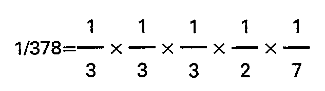

integrated frequency divider 12, the 1/3divider 62 is used commonly for the NTSC and CCIR signals, thefrequency divider 64 is operated selectively as a 1/6 divider for the NTSC signal and as a 1/5 divider for the CCIR signal, thefrequency divider 65 is switched for 1/3 and 1/5, and thefrequency divider 66 is switched for 1/7 and 1/5 for the NTSC and CCIR signals, respectively. Thefrequency divider 9 is made up of a 1/2divider 60 and a 1/4divider 61. Awaveform shaper 70 is connected between thephase selection circuit 8 and thefrequency converter 6. The input terminal 75 receives the switching signal for selecting 90° phase shift or 180° phase shift for thephase selection circuit 8, and the terminal 76 receives the switching signal for selecting NTSC or CCIR mode.Reference number 77 denotes a burst gate circuit. Thewaveform shaper 70 serves to time the leading edge of the output signal from thephase selection circuit 8. One embodiment of thewaveform shaper 70 is shown in Fig. 16, where theT terminal 72 of flip-flop 71 receives the output of the 1/2frequency divider 60, while theD terminal 73 receives the output of thephase selection circuit 8, providing a correctly timed rising signal at theoutput terminal 74. In this embodiment, N is set to 126 so that (3N-2)/4 is an integer, and the NTSC chroma signal is subjected to 180° phase shift. - Fig. 17 shows an embodiment of the best-mode NTSC chroma signal recording circuit combined with the CCIR chroma signal recording circuit, wherein the pilot signals are provided. The arrangement of Fig. 17 includes a
frequency divider 63 constituting a phase matching circuit, made up of a 1/3frequency divider 65, a 1/6divider 64 and a 1/7divider 66, and it forms a 1/126 frequency divider effectively. Thephase selection circuit 8 does not perform phase shifting for the first field and performs a 180° phase shift in every horizontal scanning period for the second field. On this account, theoscillator 10 provides the oscillation frequency of fvco=3xl26 fH=378 fH. Accordingly, the output frequency f3 of thephase selection circuit 8 becomes


second converter 2 becomes


pilot signal generator 68 has the same frequency division factors as those of the circuit shown in Fig. 13, and the pilot signal frequencies are provided as:


- Fig. 18 shows an embodiment of the
phase selection circuit 8. Figs. 19, 20 and 21 are timing charts for the arrangement of Fig. 18. - The operation in NTSC mode will first be described. In NTSC mode, the control
signal input terminal 76 receives a high level signal so as to select the frequency division factor for thefrequency divider 12 of
Signal 14a at the terminal 49 indicating the track resets the flip-flops 156 and 157 during a high period. Then the flip-flops 156 and 157 provide the output signals as shown by thewaveforms NAND gate 164 takes logical product in cooperation with inverter 125 between thesignals NAND gate 165 and inverter 176 take logical product between thesignals NAND gate 166 andinverter 177 take logical product between thesignals NAND gate 167 andinverter 178 take logical product between thesignals respective output signals - The
VCO 10 provides the oscillation frequency of 378 fH in cooperation with thefrequency divider 12 and thephase comparator 54. The output of theVCO 10 is conducted through the terminal 150 to terminal T of flip-flop 153 constituting a 1/2frequency divider 60. The Q output of the flip-flop 153 is conducted to terminal T of flip-flop 154 constituting a 1/4frequency divider 61. The same effect will result in this case when theQ output 13b of the flip-flop 153 is conducted to the T terminal of the flip-flops 154 and 155. Terminals Q and Q of the flip-flops 154 and 155 providesignals signals NAND gates 160, 161, 162 and 163, respectively, and signals 13c and 13e with a phase difference of 180° are obtained alternately in every horizontal period at the output of theNAND gate 174 during a period whensignal 14a indicating the track is low. When thesignal 14a is high, the NAND gates 163,162 and 161 are disabled, allowing theNAND gate 174 to provide normally at its output thesignal 13f. - The
NAND gates Q outputs of the flip-flop 158, and the output signals at the Q andQ terminals of theNAND gate 174 are phase-reversed each time a pulse signal is applied to the terminal 151. The signal supplied to the.terminal151 is, for example, a signal representing the discontinuity of the reproduced chroma signal which occurs when the heads are switched. The phase of the output of the flip-flop 153 is regulated by the flip-flop 71 constituting awaveform shaper 70, then conducted through the terminal 152 to thefrequency converter 6. - Next, the operation in CCIR mode will be described. This operation differs from that of NTSC mode in that the
frequency divider 12 is controlled by a low level signal at the control signal input terminal so as to select the frequency division factor of
NAND gates flop 157 to the D input of the flip-flop 156. In this case, the outputs of the flip-flops 156 and 157 have the waveforms as shown by 14b, 14c, 14d and 14e in Fig. 15. Accordingly, theinverters flops 154 and 155 providesignals signals NAND gate 174 provides at itsoutput terminal signal 14a indicating the track is low, and providessignal 13f normally during the period when thesignal 14a is high. The arrangement can readily be modified so that when thetrack indicating signal 14a is low,signals signal 13f is obtained normally when thesignal 14a is high. Thus the phase shift of both +90° and -90° can readily be realized. - As described above, when designing a magnetic recording and reproducing apparatus for recording color television signals of CCIR system, the recording chroma signal frequency is chosen to be 3/8 N · fH (where N is an odd number), whereby a large part of the lower carrier generator can be used for recording the chroma signal of NTSC system, and the chroma signals in the NTSC and CCIR color television signals can be processed by the common circuit. Similarly, in designing a magnetic recording and reproducing apparatus for recording color television signals in NTSC system, the recording chroma signal frequency is chosen to be 3/8 N . fH (where N is an integer), whereby color television signals in CCIR system can also be recorded by a slight modification of the circuit. It will be appreciated from the foregoing descriptions that the value of N is chosen so that N/4 is an integer in case of 90° phase shift or N is chosen so that (3N-2)/4 is an integer in case of 180° phase shift for recording NTSC signals. There are many values for N to take which meet the above conditions, and some examples are listed in Table 1. In Table 1, multiples of the horizontal frequency are given as 3N, which is multiplied by fH to provide the oscillation frequency of the VCO.
- Table 1 lists some preferable combinations of the color subcarrier frequencies for NTSC and CCIR systems. When selection is made giving precedence to NTSC system, mode C, D, I, J, M, N, O and P are preferable since they are achieved by using frequency dividers each having a division factor of less than 10. When selection is made giving precedence to CCIR system, mode M is preferable by the same reason. Accordingly, the best mode is M when merely considering the easiness of designing the chroma circuit.
- Table 2 lists some examples of the relationship between the color subcarrier frequency and the pilot signal frequencies which can be generated by the chroma circuit. In order to provide an enhanced servo characteristics by the pilot signals, the value of |(f2-f1)-(f4-f3)| I should be made as near zero as possible, and it should be 200 Hz (0.013 fH) as the worst case.
- Suitable modes for generating the pilot signals are
modes modes combinations 15 and 16, and 16 and 17 provide even frequency division factors for producing the pilot signals, allowing easy suppression against the generation of harmonic distortions in the pilot signals and also a simple arrangement of frequency dividers. - In Table 1, the preferable modes in consideration of both the easiness of designing the chroma circuit and the easiness of producing the pilot signals are modes I, M and N when giving precedence to NTSC system, or mode M when giving precedence to CCIR system.


Claims (2)
characterized in that


characterized in that

Priority Applications (1)
| Application Number | Priority Date | Filing Date | Title |
|---|---|---|---|
| AT82110123T ATE27883T1 (en) | 1981-11-04 | 1982-11-03 | DEVICE FOR RECORDING COLOR VIDEO SIGNALS. |
Applications Claiming Priority (12)
| Application Number | Priority Date | Filing Date | Title |
|---|---|---|---|
| JP175677/81 | 1981-11-04 | ||
| JP56175677A JPS5877390A (en) | 1981-11-04 | 1981-11-04 | Color signal recording device and method |
| JP175673/81 | 1981-11-04 | ||
| JP56175678A JPS5877391A (en) | 1981-11-04 | 1981-11-04 | NTSC chroma signal recording device and method |
| JP175678/81 | 1981-11-04 | ||
| JP56175673A JPS5877387A (en) | 1981-11-04 | 1981-11-04 | PAL color signal recording device and method |
| JP37996/82 | 1982-03-12 | ||
| JP57037994A JPS58156283A (en) | 1982-03-12 | 1982-03-12 | Chroma signal recorder |
| JP57037996A JPS58156285A (en) | 1982-03-12 | 1982-03-12 | Recorder of color signal |
| JP37994/82 | 1982-03-12 | ||
| JP57053820A JPS58172092A (en) | 1982-04-02 | 1982-04-02 | Chroma signal recording device |
| JP53820/82 | 1982-04-02 |
Publications (3)
| Publication Number | Publication Date |
|---|---|
| EP0078542A2 EP0078542A2 (en) | 1983-05-11 |
| EP0078542A3 EP0078542A3 (en) | 1984-08-22 |
| EP0078542B1 true EP0078542B1 (en) | 1987-06-16 |
Family
ID=27549884
Family Applications (1)
| Application Number | Title | Priority Date | Filing Date |
|---|---|---|---|
| EP82110123A Expired EP0078542B1 (en) | 1981-11-04 | 1982-11-03 | Color video signal recording apparatus |
Country Status (6)
| Country | Link |
|---|---|
| US (1) | US4554596A (en) |
| EP (1) | EP0078542B1 (en) |
| AU (1) | AU542594B2 (en) |
| BR (1) | BR8206389A (en) |
| CA (1) | CA1192996A (en) |
| DE (1) | DE3276606D1 (en) |
Families Citing this family (7)
| Publication number | Priority date | Publication date | Assignee | Title |
|---|---|---|---|---|
| JPS59141880A (en) * | 1983-02-01 | 1984-08-14 | Canon Inc | Automatic tracking method |
| US4647983A (en) * | 1983-09-30 | 1987-03-03 | Victor Company Of Japan Ltd. | Method and apparatus for recording and/or reproducing color video signal |
| JPH067687B2 (en) * | 1984-04-16 | 1994-01-26 | 松下電器産業株式会社 | Color signal processor |
| JPS63102481A (en) * | 1986-10-18 | 1988-05-07 | Pioneer Electronic Corp | Multiplex recording system |
| DE3854808T2 (en) * | 1987-10-08 | 1996-05-15 | Victor Company Of Japan | Video tape recorder with a pilot signal control function for selecting luminance signal filter characteristics during playback |
| US5621537A (en) * | 1989-11-02 | 1997-04-15 | Mitsubishi Denki Kabushiki Kaisha | Color signal processing circuit in color VTR |
| JPH06327028A (en) * | 1993-03-17 | 1994-11-25 | Sanyo Electric Co Ltd | Adjusting circuit using color burst signal |
Family Cites Families (7)
| Publication number | Priority date | Publication date | Assignee | Title |
|---|---|---|---|---|
| JPS5422059B2 (en) * | 1972-05-22 | 1979-08-03 | ||
| GB1497865A (en) * | 1973-12-28 | 1978-01-12 | Sony Corp | Magnetic recording and/or reproducing apparatus |
| DE2652905A1 (en) * | 1976-11-20 | 1978-07-06 | Bosch Gmbh Robert | Colour TV signals transcoding system - separates chrominance signal and mixed signals by NTSC method, and passes them through band-pass filter and again mixes them |
| JPS53104214A (en) * | 1977-02-24 | 1978-09-11 | Sony Corp | Magnetic recorder |
| US4220964A (en) * | 1977-11-21 | 1980-09-02 | Sony Corporation | Secam recording and reproducing system |
| GB2040135B (en) * | 1979-01-05 | 1983-05-05 | Victor Company Of Japan | Pal system colour video signal recording |
| JPS5636290A (en) * | 1979-09-03 | 1981-04-09 | Matsushita Electric Ind Co Ltd | Recording and reproducing device with image pickup function |
-
1982
- 1982-11-01 US US06/438,246 patent/US4554596A/en not_active Expired - Lifetime
- 1982-11-03 DE DE8282110123T patent/DE3276606D1/en not_active Expired
- 1982-11-03 CA CA000414756A patent/CA1192996A/en not_active Expired
- 1982-11-03 EP EP82110123A patent/EP0078542B1/en not_active Expired
- 1982-11-03 BR BR8206389A patent/BR8206389A/en not_active IP Right Cessation
- 1982-11-04 AU AU90148/82A patent/AU542594B2/en not_active Ceased
Also Published As
| Publication number | Publication date |
|---|---|
| CA1192996A (en) | 1985-09-03 |
| AU9014882A (en) | 1983-05-26 |
| US4554596A (en) | 1985-11-19 |
| EP0078542A3 (en) | 1984-08-22 |
| BR8206389A (en) | 1983-09-27 |
| AU542594B2 (en) | 1985-02-28 |
| EP0078542A2 (en) | 1983-05-11 |
| DE3276606D1 (en) | 1987-07-23 |
Similar Documents
| Publication | Publication Date | Title |
|---|---|---|
| CA1124835A (en) | Secam recording and reproducing system | |
| US4554596A (en) | Color video signal recording apparatus | |
| US4661863A (en) | Color video signal recording and reproducing apparatus | |
| GB1412091A (en) | Systems for recording and reproducing colour television signals | |
| KR880000865B1 (en) | Video disc player with auxiliary vertical sync generator | |
| US4079412A (en) | Signal processing circuit in a color video signal recording and/or reproducing apparatus | |
| US4593327A (en) | Color video signal recording and/or reproducing system | |
| US5083213A (en) | Chrominance signal processing circuit and video tape recorder having function of processing chrominance signal | |
| US4646165A (en) | Chrominance signal recording apparatus utilizing digital sampling and quantizing techniques | |
| EP0091102B1 (en) | Color signal processing circuit for video tape recorders | |
| KR850001024B1 (en) | Color video signal recording device | |
| JPH0421399B2 (en) | ||
| US4745493A (en) | Circuit arrangement for a color image recording and reproduction instrument or a color television receiver | |
| KR910005253B1 (en) | Low-frequency converter for carrier chrominance signal | |
| US4480265A (en) | PAL Comb filter | |
| JPS6132876B2 (en) | ||
| JP3244437B2 (en) | Clock generation circuit and method | |
| JPH046319B2 (en) | ||
| JPH046318B2 (en) | ||
| EP0024869B1 (en) | Video signal recording and reproducing apparatus | |
| JP2905244B2 (en) | Color signal processing device | |
| JPS6012836B2 (en) | SECAM color video signal frequency conversion circuit | |
| JP2918603B2 (en) | Color signal processing device | |
| KR800001581B1 (en) | Frequency conversion circuit of carrier color signal | |
| KR980013450A (en) | Frequency conversion circuit of color signal |
Legal Events
| Date | Code | Title | Description |
|---|---|---|---|
| PUAI | Public reference made under article 153(3) epc to a published international application that has entered the european phase |
Free format text: ORIGINAL CODE: 0009012 |
|
| AK | Designated contracting states |
Designated state(s): AT CH DE FR GB IT LI NL SE |
|
| PUAL | Search report despatched |
Free format text: ORIGINAL CODE: 0009013 |
|
| AK | Designated contracting states |
Designated state(s): AT CH DE FR GB IT LI NL SE |
|
| 17P | Request for examination filed |
Effective date: 19850208 |
|
| GRAA | (expected) grant |
Free format text: ORIGINAL CODE: 0009210 |
|
| AK | Designated contracting states |
Kind code of ref document: B1 Designated state(s): AT CH DE FR GB IT LI NL SE |
|
| REF | Corresponds to: |
Ref document number: 27883 Country of ref document: AT Date of ref document: 19870715 Kind code of ref document: T |
|
| REF | Corresponds to: |
Ref document number: 3276606 Country of ref document: DE Date of ref document: 19870723 |
|
| ET | Fr: translation filed | ||
| ITF | It: translation for a ep patent filed | ||
| PLBE | No opposition filed within time limit |
Free format text: ORIGINAL CODE: 0009261 |
|
| STAA | Information on the status of an ep patent application or granted ep patent |
Free format text: STATUS: NO OPPOSITION FILED WITHIN TIME LIMIT |
|
| 26N | No opposition filed | ||
| ITTA | It: last paid annual fee | ||
| PGFP | Annual fee paid to national office [announced via postgrant information from national office to epo] |
Ref country code: SE Payment date: 19930927 Year of fee payment: 12 |
|
| PGFP | Annual fee paid to national office [announced via postgrant information from national office to epo] |
Ref country code: AT Payment date: 19931126 Year of fee payment: 12 |
|
| PGFP | Annual fee paid to national office [announced via postgrant information from national office to epo] |
Ref country code: NL Payment date: 19931130 Year of fee payment: 12 |
|
| PGFP | Annual fee paid to national office [announced via postgrant information from national office to epo] |
Ref country code: CH Payment date: 19940127 Year of fee payment: 12 |
|
| PG25 | Lapsed in a contracting state [announced via postgrant information from national office to epo] |
Ref country code: AT Effective date: 19941103 |
|
| PG25 | Lapsed in a contracting state [announced via postgrant information from national office to epo] |
Ref country code: SE Effective date: 19941104 |
|
| PG25 | Lapsed in a contracting state [announced via postgrant information from national office to epo] |
Ref country code: LI Effective date: 19941130 Ref country code: CH Effective date: 19941130 |
|
| EAL | Se: european patent in force in sweden |
Ref document number: 82110123.5 |
|
| PG25 | Lapsed in a contracting state [announced via postgrant information from national office to epo] |
Ref country code: NL Effective date: 19950601 |
|
| NLV4 | Nl: lapsed or anulled due to non-payment of the annual fee | ||
| REG | Reference to a national code |
Ref country code: CH Ref legal event code: PL |
|
| EUG | Se: european patent has lapsed |
Ref document number: 82110123.5 |
|
| PGFP | Annual fee paid to national office [announced via postgrant information from national office to epo] |
Ref country code: FR Payment date: 20010919 Year of fee payment: 20 |
|
| PGFP | Annual fee paid to national office [announced via postgrant information from national office to epo] |
Ref country code: GB Payment date: 20011024 Year of fee payment: 20 |
|
| PGFP | Annual fee paid to national office [announced via postgrant information from national office to epo] |
Ref country code: DE Payment date: 20011227 Year of fee payment: 20 |
|
| REG | Reference to a national code |
Ref country code: GB Ref legal event code: IF02 |
|
| PG25 | Lapsed in a contracting state [announced via postgrant information from national office to epo] |
Ref country code: GB Free format text: LAPSE BECAUSE OF EXPIRATION OF PROTECTION Effective date: 20021102 |
|
| REG | Reference to a national code |
Ref country code: GB Ref legal event code: PE20 Effective date: 20021102 |