EP0071204B1 - Method for forming recessed dielectric isolation - Google Patents
Method for forming recessed dielectric isolation Download PDFInfo
- Publication number
- EP0071204B1 EP0071204B1 EP82106655A EP82106655A EP0071204B1 EP 0071204 B1 EP0071204 B1 EP 0071204B1 EP 82106655 A EP82106655 A EP 82106655A EP 82106655 A EP82106655 A EP 82106655A EP 0071204 B1 EP0071204 B1 EP 0071204B1
- Authority
- EP
- European Patent Office
- Prior art keywords
- glass
- trenches
- silicon
- forming
- isolation
- Prior art date
- Legal status (The legal status is an assumption and is not a legal conclusion. Google has not performed a legal analysis and makes no representation as to the accuracy of the status listed.)
- Expired
Links
Images

Classifications
-
- H—ELECTRICITY
- H01—ELECTRIC ELEMENTS
- H01L—SEMICONDUCTOR DEVICES NOT COVERED BY CLASS H10
- H01L21/00—Processes or apparatus adapted for the manufacture or treatment of semiconductor or solid state devices or of parts thereof
- H01L21/02—Manufacture or treatment of semiconductor devices or of parts thereof
- H01L21/02104—Forming layers
- H01L21/02107—Forming insulating materials on a substrate
- H01L21/02109—Forming insulating materials on a substrate characterised by the type of layer, e.g. type of material, porous/non-porous, pre-cursors, mixtures or laminates
- H01L21/02112—Forming insulating materials on a substrate characterised by the type of layer, e.g. type of material, porous/non-porous, pre-cursors, mixtures or laminates characterised by the material of the layer
- H01L21/02123—Forming insulating materials on a substrate characterised by the type of layer, e.g. type of material, porous/non-porous, pre-cursors, mixtures or laminates characterised by the material of the layer the material containing silicon
- H01L21/02142—Forming insulating materials on a substrate characterised by the type of layer, e.g. type of material, porous/non-porous, pre-cursors, mixtures or laminates characterised by the material of the layer the material containing silicon the material containing silicon and at least one metal element, e.g. metal silicate based insulators or metal silicon oxynitrides
- H01L21/02145—Forming insulating materials on a substrate characterised by the type of layer, e.g. type of material, porous/non-porous, pre-cursors, mixtures or laminates characterised by the material of the layer the material containing silicon the material containing silicon and at least one metal element, e.g. metal silicate based insulators or metal silicon oxynitrides the material containing aluminium, e.g. AlSiOx
-
- H—ELECTRICITY
- H01—ELECTRIC ELEMENTS
- H01L—SEMICONDUCTOR DEVICES NOT COVERED BY CLASS H10
- H01L21/00—Processes or apparatus adapted for the manufacture or treatment of semiconductor or solid state devices or of parts thereof
- H01L21/02—Manufacture or treatment of semiconductor devices or of parts thereof
- H01L21/02104—Forming layers
- H01L21/02107—Forming insulating materials on a substrate
- H01L21/02225—Forming insulating materials on a substrate characterised by the process for the formation of the insulating layer
- H01L21/0226—Forming insulating materials on a substrate characterised by the process for the formation of the insulating layer formation by a deposition process
- H01L21/02263—Forming insulating materials on a substrate characterised by the process for the formation of the insulating layer formation by a deposition process deposition from the gas or vapour phase
- H01L21/02266—Forming insulating materials on a substrate characterised by the process for the formation of the insulating layer formation by a deposition process deposition from the gas or vapour phase deposition by physical ablation of a target, e.g. sputtering, reactive sputtering, physical vapour deposition or pulsed laser deposition
-
- H—ELECTRICITY
- H01—ELECTRIC ELEMENTS
- H01L—SEMICONDUCTOR DEVICES NOT COVERED BY CLASS H10
- H01L21/00—Processes or apparatus adapted for the manufacture or treatment of semiconductor or solid state devices or of parts thereof
- H01L21/02—Manufacture or treatment of semiconductor devices or of parts thereof
- H01L21/02104—Forming layers
- H01L21/02107—Forming insulating materials on a substrate
- H01L21/02225—Forming insulating materials on a substrate characterised by the process for the formation of the insulating layer
- H01L21/0226—Forming insulating materials on a substrate characterised by the process for the formation of the insulating layer formation by a deposition process
- H01L21/02263—Forming insulating materials on a substrate characterised by the process for the formation of the insulating layer formation by a deposition process deposition from the gas or vapour phase
- H01L21/02271—Forming insulating materials on a substrate characterised by the process for the formation of the insulating layer formation by a deposition process deposition from the gas or vapour phase deposition by decomposition or reaction of gaseous or vapour phase compounds, i.e. chemical vapour deposition
-
- H—ELECTRICITY
- H01—ELECTRIC ELEMENTS
- H01L—SEMICONDUCTOR DEVICES NOT COVERED BY CLASS H10
- H01L21/00—Processes or apparatus adapted for the manufacture or treatment of semiconductor or solid state devices or of parts thereof
- H01L21/02—Manufacture or treatment of semiconductor devices or of parts thereof
- H01L21/02104—Forming layers
- H01L21/02107—Forming insulating materials on a substrate
- H01L21/02225—Forming insulating materials on a substrate characterised by the process for the formation of the insulating layer
- H01L21/0226—Forming insulating materials on a substrate characterised by the process for the formation of the insulating layer formation by a deposition process
- H01L21/02282—Forming insulating materials on a substrate characterised by the process for the formation of the insulating layer formation by a deposition process liquid deposition, e.g. spin-coating, sol-gel techniques, spray coating
-
- H—ELECTRICITY
- H01—ELECTRIC ELEMENTS
- H01L—SEMICONDUCTOR DEVICES NOT COVERED BY CLASS H10
- H01L21/00—Processes or apparatus adapted for the manufacture or treatment of semiconductor or solid state devices or of parts thereof
- H01L21/02—Manufacture or treatment of semiconductor devices or of parts thereof
- H01L21/02104—Forming layers
- H01L21/02107—Forming insulating materials on a substrate
- H01L21/02296—Forming insulating materials on a substrate characterised by the treatment performed before or after the formation of the layer
- H01L21/02299—Forming insulating materials on a substrate characterised by the treatment performed before or after the formation of the layer pre-treatment
- H01L21/02304—Forming insulating materials on a substrate characterised by the treatment performed before or after the formation of the layer pre-treatment formation of intermediate layers, e.g. buffer layers, layers to improve adhesion, lattice match or diffusion barriers
-
- H—ELECTRICITY
- H01—ELECTRIC ELEMENTS
- H01L—SEMICONDUCTOR DEVICES NOT COVERED BY CLASS H10
- H01L21/00—Processes or apparatus adapted for the manufacture or treatment of semiconductor or solid state devices or of parts thereof
- H01L21/02—Manufacture or treatment of semiconductor devices or of parts thereof
- H01L21/04—Manufacture or treatment of semiconductor devices or of parts thereof the devices having at least one potential-jump barrier or surface barrier, e.g. PN junction, depletion layer or carrier concentration layer
- H01L21/18—Manufacture or treatment of semiconductor devices or of parts thereof the devices having at least one potential-jump barrier or surface barrier, e.g. PN junction, depletion layer or carrier concentration layer the devices having semiconductor bodies comprising elements of Group IV of the Periodic System or AIIIBV compounds with or without impurities, e.g. doping materials
- H01L21/30—Treatment of semiconductor bodies using processes or apparatus not provided for in groups H01L21/20 - H01L21/26
- H01L21/31—Treatment of semiconductor bodies using processes or apparatus not provided for in groups H01L21/20 - H01L21/26 to form insulating layers thereon, e.g. for masking or by using photolithographic techniques; After treatment of these layers; Selection of materials for these layers
- H01L21/3105—After-treatment
-
- H—ELECTRICITY
- H01—ELECTRIC ELEMENTS
- H01L—SEMICONDUCTOR DEVICES NOT COVERED BY CLASS H10
- H01L21/00—Processes or apparatus adapted for the manufacture or treatment of semiconductor or solid state devices or of parts thereof
- H01L21/02—Manufacture or treatment of semiconductor devices or of parts thereof
- H01L21/04—Manufacture or treatment of semiconductor devices or of parts thereof the devices having at least one potential-jump barrier or surface barrier, e.g. PN junction, depletion layer or carrier concentration layer
- H01L21/18—Manufacture or treatment of semiconductor devices or of parts thereof the devices having at least one potential-jump barrier or surface barrier, e.g. PN junction, depletion layer or carrier concentration layer the devices having semiconductor bodies comprising elements of Group IV of the Periodic System or AIIIBV compounds with or without impurities, e.g. doping materials
- H01L21/30—Treatment of semiconductor bodies using processes or apparatus not provided for in groups H01L21/20 - H01L21/26
- H01L21/31—Treatment of semiconductor bodies using processes or apparatus not provided for in groups H01L21/20 - H01L21/26 to form insulating layers thereon, e.g. for masking or by using photolithographic techniques; After treatment of these layers; Selection of materials for these layers
- H01L21/314—Inorganic layers
- H01L21/316—Inorganic layers composed of oxides or glassy oxides or oxide based glass
- H01L21/31604—Deposition from a gas or vapour
- H01L21/31608—Deposition of SiO2
-
- H—ELECTRICITY
- H01—ELECTRIC ELEMENTS
- H01L—SEMICONDUCTOR DEVICES NOT COVERED BY CLASS H10
- H01L21/00—Processes or apparatus adapted for the manufacture or treatment of semiconductor or solid state devices or of parts thereof
- H01L21/70—Manufacture or treatment of devices consisting of a plurality of solid state components formed in or on a common substrate or of parts thereof; Manufacture of integrated circuit devices or of parts thereof
- H01L21/71—Manufacture of specific parts of devices defined in group H01L21/70
- H01L21/76—Making of isolation regions between components
- H01L21/762—Dielectric regions, e.g. EPIC dielectric isolation, LOCOS; Trench refilling techniques, SOI technology, use of channel stoppers
- H01L21/76224—Dielectric regions, e.g. EPIC dielectric isolation, LOCOS; Trench refilling techniques, SOI technology, use of channel stoppers using trench refilling with dielectric materials
- H01L21/76232—Dielectric regions, e.g. EPIC dielectric isolation, LOCOS; Trench refilling techniques, SOI technology, use of channel stoppers using trench refilling with dielectric materials of trenches having a shape other than rectangular or V-shape, e.g. rounded corners, oblique or rounded trench walls
-
- H—ELECTRICITY
- H01—ELECTRIC ELEMENTS
- H01L—SEMICONDUCTOR DEVICES NOT COVERED BY CLASS H10
- H01L21/00—Processes or apparatus adapted for the manufacture or treatment of semiconductor or solid state devices or of parts thereof
- H01L21/70—Manufacture or treatment of devices consisting of a plurality of solid state components formed in or on a common substrate or of parts thereof; Manufacture of integrated circuit devices or of parts thereof
- H01L21/71—Manufacture of specific parts of devices defined in group H01L21/70
- H01L21/76—Making of isolation regions between components
- H01L21/762—Dielectric regions, e.g. EPIC dielectric isolation, LOCOS; Trench refilling techniques, SOI technology, use of channel stoppers
- H01L21/76224—Dielectric regions, e.g. EPIC dielectric isolation, LOCOS; Trench refilling techniques, SOI technology, use of channel stoppers using trench refilling with dielectric materials
- H01L21/76237—Dielectric regions, e.g. EPIC dielectric isolation, LOCOS; Trench refilling techniques, SOI technology, use of channel stoppers using trench refilling with dielectric materials introducing impurities in trench side or bottom walls, e.g. for forming channel stoppers or alter isolation behavior
Definitions
- the invention relates to methods for dielectrically isolating regions of monocrystalline silicon from other regions of monocrystalline silicon and more particularly to techniques which completely overcome the "bird's beak" problem while reducing stresses in the semiconductor structure.
- One form of dielectric isolation involves the formation of grooves or depressions in silicon where the isolation regions are to be formed. During the groove formation, the remainder of the silicon surface is protected by a protective film which is substantially unaffected by the silicon etch used to form the grooves.
- the usual protective layer is a silicon nitride, silicon dioxide sandwich layer.
- the silicon body is subjected to a conventional oxidation step whereby the silicon in the groove area is oxidized and the silicon dioxide fills up the groove as well as oxidizing further into the silicon to form the isolation region.
- One of the major problems with this process is what is known as "bird's beak".
- the "bird's beak” is a non-planar silicon dioxide formation at the top periphery of the groove and is caused by the lateral oxidation underneath the silicon dioxide layer. Since the oxidation of a specific thickness of silicon requires an almost equivalent amount of free space to expand into, and since the Si0 2 /Si 3 N 4 limits the unrestricted expansion, the result is an up-pushing of the silicon dioxide/silicon nitride at the edge of the groove. The final consequence of this is a general stress in the perimeter region of the groove as well as difficulties in subsequently achieving good abutted diffusions against the vertical portion of the silicon dioxide. This non-abutting capability defeats a major benefit of the original purpose of the silicon dioxide region.
- An alternate to recessed oxide isolation is deep dielectric isolation which involves the formation of rectangular grooves made in U.S. Patents 3 966 577, 3 997 378, 4104 086 and S. A. Abbas, IBM TDB Vol. 20, No. 1, p. 144, June 1977 entitled "Recessed Oxide Isolation Process", by reactive ion etching techniques and filling the grooves to form the isolation for the silicon regions.
- the groove filling techniques all involve either thermal oxidation and/or chemical vapor deposition techniques and extensively use silicon dioxide as the dielectric isolation.
- a method of trench refill with deposited glasses is known from IBM Technical Disclosure Bulletin, Vol. 23, March 1981, pages 4745-4747.
- Object of the invention is a method for forming recessed dielectric isolation which avoids the afore mentioned disadvantages of prior art recessed dielectric isolation methods.
- the object of the invention is achieved by a method according to claim 1.
- the recessed dielectric type of isolation is of the order of 1 micrometer in depth or less as compared to what is termed deep dielectric isolation which extends into the silicon substrate 3 to 5 micrometers or more.
- the method for forming the recessed dielectric isolation in a silicon substrate (2) involves first forming trenches (16) which are less than about 1 micrometer in depth in areas of one principal surface of the silicon substrate where isolation is desired.
- trenches (16) which are less than about 1 micrometer in depth in areas of one principal surface of the silicon substrate where isolation is desired.
- a bipolar transistor structure is planned to be formed it is usually necessary to have a P+ region (6) underneath the recessed dielectric isolation to allow full isolation between the various NPN bipolar transistor devices.
- To make a PNP transistor it is necessary to use a N+ region underneath the isolation. Under the circumstance the P+ region is formed in the substrate prior to the deposition of an epitaxial layer thereover.
- the trench formation is caused to be formed through the epitaxial layer (8) and into the P+ regions (6) therein.
- the surfaces of the trenches are then oxidized in an oxidizing ambient to form a silicon dioxide layer (18) thereon.
- a glass (20) is deposited over this principal surface.
- the glass used has a thermal coefficient of expansion that approximates that of silicon and has a softening temperature of less than about 1200°C.
- the structure is then heated to a temperature that allows the flow of the deposited glass on the surface so as to fill the trenches.
- the glass on the principal surface above the trench can be removed by a reactive ion etching method. Alternatively and preferably the glass is removed from areas other than the immediate area of the trench by lithography and etching techniques followed by a second heating of the structure to cause the glass flow to result in surface planarization.
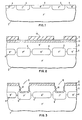
- Figures 1 through 6 illustrate a first method embodiment of forming the recessed dielectric isolation intended for bipolar transistor purposes.
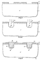
- Figures 7 through 9 show a second embodiment of the formation of recessed dielectric isolation of the present invention particularly useful for use with field effect transistor devices.
- a semiconductor body 2 of a P-conductivity type is typically ⁇ 100> crystallographically oriented silicon and of a resistivity in the order of 1 to 20 ohm-cm.
- Conventional lithography and etching techniques are utilized to form the mask for the subcollector diffusion step.
- N type impurities are then diffused by conventional techniques to form a region 4 having a surface concentration level of typically 5x10 20 atoms/cc.
- the N type impurity may be, for example, arsenic or antimony.
- the structure is now subjected to a thermal oxidation to form silicon dioxide thereover.
- the N type impurity is driven further into the semiconductor body.
- the silicon dioxide layer is now formed into a diffusion mask using conventional lithography and etching techniques.
- the body is now subjected to a diffusion of P type impurity, such as boron, prefereably of a high concentration level, such as 3X10 20 atoms/cc at the surface of the exposed silicon regions to form P+ regions 6 which will ultimately form part of the recessed dielectric isolation and junction isolation regions between devices of the semiconductor bipolar structure.
- the silicon dioxide layer on the surface of the silicon body is removed by use of conventional etching techniques.
- the silicon body is then placed in an epitaxial growth chamber and a monocrystalline silicon layer 8 is grown upon the principal surface of the silicon body having the diffusions 4 and 6 therein.
- This growth is done by conventional techniques such as the use of SiCl 4 /H 2 or SiH 4 /H 2 mixtures at growth temperatures of about 1000°C to 1200°C.
- the thickness of the epitaxial layer is typically 2 micrometers but may be in the range of 0.5 to 10 micrometers.
- the epitaxial layer is doped with an N type impurity of a low concentration level which is typically 2x 10 16 atoms/cc.
- the N+ region 4 and the P+ diffused region 6 move into the epitaxial layerto fully form the final N+ region 4 and P+ region 6 as illustrated in Figure 2.
- Silicon dioxide layer 10 is formed by conventional techniques of either thermal growth at a temperature of about 970°C in wet or dry oxygen ambient or by chemical vapor deposition.
- the silicon nitride layer 12 is formed thereover typically by a chemical vapor deposition.
- a resist layer 14 is deposited over layer 12. This layer is then formed into a mask using conventional lithography techniques so that openings are provided directly above the P+ buried regions 6 as shown in Figure 2.
- the layers 10 and 12 are etched using conventional chemical, reactive ion etching or plasma etching techniques at the openings of resist layer 14 down to the monocrystalline silicon substrate.
- the structure is now ready to utilize the layers 10, 12 as the mask for the trench 16 formation following the removal of the resist layer 14 from the surface of layer 12.
- This process may be accomplished using chemical etching but this type of etching causes the walls of the trenches 16 to become more inclined than in the case of use of reactive ion etching.
- the trenches 16 are preferably formed by reactive ion etching (RIE) which produces substantially vertical sidewalls for the trenches.
- RIE reactive ion etching
- One suitable example of forming the trenches 16 by RIE is the use of carbontetrafluoride (CF 4 ) gas.
- gases include CCL 4 -Ar and CI z -Ar. Details of the RIE are described in German Auslegeschrift 26 17 483.
- a layer 18 of silicon dioxide is preferably formed by thermal oxidation in steam at a temperature of about 970°C on the surface of the trenches.
- the layer 18 of silicon dioxide may alternatively be formed by chemical vapor deposition but this would necessitate the removal of the deposited silicon dioxide from the layer 12 surface.
- the preferred thickness of the layer 18 of the silicon dioxide is preferably in the range of 100 to 500 nm. It may also be desirable to form a silicon nitride layer (not shown) on the surface of this silicon dioxide layer 18 to prevent the movement of any unwanted impurities, such as sodium ions, from the glass recessed dielectric isolation through the silicon dioxide into the silicon body.
- This silicon nitride layer can be deposited by conventional chemical vapor deposition techniques. The result of the process is shown in Figure 3.
- the Figure 3 structure is now ready to be filled with a dielectric glass material having a thermal coefficient of expansion that approximates that of silicon.
- the preferred range of the coefficient is between about 20 to 50x10 -7 per degree centigrade.
- the other important criterion for this glass material is its softening temperature and its ability to flow upon heating to that softening temperature or above. Examples of glasses which will act according to these criterion are given in Tables I, II and III.
- the listed glasses merely are illustrative of glasses which can be used in this invention.
- the Table I gives examples of borosilicate, lead borosilicate and calcium alumino borosilicate glasses.
- the Table II lists glass-ceramics of the (3-spodumene type.
- the Table III lists glass-ceramics of the cordierite type. The Tables II and III were taken from U.S. Patent 4 301 324.
- the silicon dioxide layer 18 in Figure 3 can be capped by depositing a thin silicon nitride layer of the order of 50 to 150 nm by chemical vapor deposition techniques. This silicon nitride layer will serve as barrier to the diffusion of impurities into the Si0 2 layer from the glass.
- FIG. 4 there is shown the result of the deposition and first heating step of a glass layer 20 which fills the trenches 16 and covers the surface of the semiconductor integrated circuit.
- a glass layer 20 which fills the trenches 16 and covers the surface of the semiconductor integrated circuit.
- One technqiue utilizes the sedimentation, centrifugation or spin-on of colloidal glass particles.
- Other methods would include the sputtering or evaporation of the glass onto a semiconductor silicon surface.
- Sedimentation techniques by centrifugation are supplied generally in U.S. Patents 3 212 921 and 3 212 929. Glass sedimentation is described in Pliskin and Conrad “Techniques for Obtaining Uniform Thin Glass Film on Substrates", Electrochemical Technology, Vol. 2, No. 7-8, pages 196-200 (1964). Spin-on techniques are described in J. A. Amick et. al., J. Vac. Soc. Tech. 14, No. 5, page 1053 (1977). In accordance with this known technology, a finally ground glass powder having properties providing a better match to silicon is employed as illustrated in the Table I. The glass power is ultrasonically mixed with a reasonably high dielectric medium. Typically, such a liquid is isopropyl alcohol.
- a lower dielectric constant fluid such as ethyl acetate is added and is ultrasonically mixed with the other materials.
- a medium rotate speed for example at 500 G (gravitation) is utilized and the decanted liquid suspension obtained has fine particles of glass desirable for the glass deposition process. These steps may be repeated to obtain better separation and finer particles in the suspension which hereinafter will be referred to as the "concentrate".
- the glass suspension concentrate will then be coated onto the substrate in accordance with any of the above referenced techniques.
- the structure is then fired for a few minutes at a temperature above the softening point of the glass to form a clear glass film.
- Sputtering methods would be used for depositing the glass by forming a target of the glass material and subsequently applying R.F.
- the sputtering process for insulators such as the glasses of the present invention is described in detail in the Handbook of Thin Film Technology, by L. I. Maissel et. al., published by McGraw Hill Book Co., New York, NY, 1970, pages 4-31 through 4-44.
- the evaporation method for deposition of these glasses use the E-beam evaporation technique.
- the films so formed would contour to the topography to a greater extent than by the previously mentioned methods. Fusing the glass film will correspondingly flow the glass.
- the methods for E-beam evaporation of these materials can be better understood with reference to pages 1-65 through 1-73 of the above-cited Handbook of Thin Film Technology and the W. Fedrowitz et. al. paper entitled "The Evaporation Capability of Various Glasses", published in Thin Solid Films, 72 (1980) pages 485 through 486.
- the chemical vapor deposited (CVD) method would not use the explicit compositions of Tables I, II and III but essentially deposits the major constituents, for example Si0 2 , B 2 0 3 , A1 2 0 3 to form the desired glass with the needed thermal coefficient of expansion and softening point. This would be accomplished, for example, by the conventional use of SiH 4 , B 2 H 6 , AI(OC 8 H I ) 3 and N 2 0 with the concentrations of the B and AI in the approximate ranges shown in the Tables.
- the method for CVD of glass of the present type can be more fully understood with reference to "Materials, Properties and Preparation", Vol. 3, by S. P. Keller published by North-Holland Pub. Co., Amsterdam, New York, Oxford, 1980, pages 651 through 653 and Amick et. al. J. Vac. Sci. Technol. 14 (1977) page 1053.
- the structure is planarized by heating the structure above the softening point of the glass layer 20. At this temperature the softened glass will flow to approach planarity as shown in Figure 4.
- the next step is the methods for making the glass filled trench substantially planar with the surface of the masking layer 10, 12. It is preferred to do this by first reducing the glass layer thickness by any of the usual etching methods, that is chemical, plasma or reactive ion etching down to thickness 28 and then by removing the glass from the surface by etching in areas other than in the immediate areas of the trenches as shown in Figure 5.
- the structure is now subjected again to heating to a temperature above the softening point of the glass. The result of this heating is the formation of a substantially planar surface of glass layer 22 over the masking layers 10, 12 as shown in Figure 6.
- the glass layer can be removed using any of the usual etching methods including chemical, plasma or reactive ion etching down to the silicon nitride layer 12 which acts as an etch stop. Still another alternative is to etch by any one or a combination of techniques through the glass layer 22, silicon nitride layer 12 and silicon dioxide layer 10 down to the silicon surface plane.
- Typical plasma and reactive ion etching systems that can be used for this process could include any one of the following gases:
- Bipolar transistors and the like can now be formed in the dielectrically isolated regions 25 wherein the N+ region 4 is the buried subcollector for such devices.
- the layers 22, 12 and 10 Prior to such formation the layers 22, 12 and 10 have to be removed by conventional etching techniques as described above. Isolation of the emitter-base region from the collector reach-through region can alternatively be made by extending the buried subcollector region 4 under a dielectrically isolated region that does not have a P+ junction isolation thereunder in the NPN transistor alternative, for example. The emitter-base region will then be surface isolated from the collector reach-through contact but the base-collector connection is effected through the subcollector region under the recessed dielectric isolation.
- the silicon substrate utilized for this type of technology is typically a P- doped substrate having a resistivity of about 1 to 20 ohm-centimeters.
- Silicon dioxide layers 10 and silicon nitride layer 12 are deposited as described with reference to the example of Figures 1 through 6. Lithography techniques are utilized to form the layers 10, 12 into a mask having openings located where recessed dielectric isolation is desired as shown in Figure 7. The mask is then utilized as described in the first embodiment to form a trench in the silicon by either chemical or reactive ion etching techniques as described in that embodiment.
- a channel stop 30 is formed beneath the bottom wall of each of the trenches 16.
- the channel stop 30 is preferably formed by implantation of boron ions having a dose or concentration of about 1 X10 19 atoms/cc. This provides each of the channel stops 30 as a P+ area in the P- substrate 2. This channel stop structure avoids any possibility of short circuiting between the various semiconductor isolated regions.
- the glass deposition of glass material 50 is made according to the same procedures as described in regard to the first embodiment.
- the heating and planarizing steps result in the final isolated structure as shown in Figure 9.
- the glass layer 52 and the silicon nitride layer 12 is now removed from the surface as described above when describing the first embodiment.
- the structure is now ready to receive the process for forming the desired field effect transistor devices.
Description
- The invention relates to methods for dielectrically isolating regions of monocrystalline silicon from other regions of monocrystalline silicon and more particularly to techniques which completely overcome the "bird's beak" problem while reducing stresses in the semiconductor structure.
- In the monolithic integrated circuit technology, it is usually necessary to isolate various active and passive elements from one another in the integrated circuit structure. These devices have been isolated by back-biasing PN junctions, partial dielectric isolation and complete dielectric isolation. The dielectric materials used have been silicon dioxide and the like. The preferred isolation for these active devices and circuits is some form of dielectric isolation. The dielectric isolation has the substantial advantage over the PN junction isolation because it allows the abutting of the circuit elements against the isolation and thereby result in greater density of packing of the active and passive devices on the integrated circuit chip.
- One form of dielectric isolation involves the formation of grooves or depressions in silicon where the isolation regions are to be formed. During the groove formation, the remainder of the silicon surface is protected by a protective film which is substantially unaffected by the silicon etch used to form the grooves. The usual protective layer is a silicon nitride, silicon dioxide sandwich layer. Following the formation of the grooves by conventional chemical etching, the silicon body is subjected to a conventional oxidation step whereby the silicon in the groove area is oxidized and the silicon dioxide fills up the groove as well as oxidizing further into the silicon to form the isolation region. One of the major problems with this process is what is known as "bird's beak".
- The "bird's beak" is a non-planar silicon dioxide formation at the top periphery of the groove and is caused by the lateral oxidation underneath the silicon dioxide layer. Since the oxidation of a specific thickness of silicon requires an almost equivalent amount of free space to expand into, and since the Si02/Si3N4 limits the unrestricted expansion, the result is an up-pushing of the silicon dioxide/silicon nitride at the edge of the groove. The final consequence of this is a general stress in the perimeter region of the groove as well as difficulties in subsequently achieving good abutted diffusions against the vertical portion of the silicon dioxide. This non-abutting capability defeats a major benefit of the original purpose of the silicon dioxide region. This process is described more fully in U.S. Patents 3 970 486, 3 534 234, 3 648 125 and
German Auslegeschrift 22 18 892. Efforts to minimize this "bird's beak" problem have been extensive and include U.S. Patents 3 900 350, 3 958 040, 3 961 999, 3 966 514, 4 002 511, and 4 170 492. - An alternate to recessed oxide isolation is deep dielectric isolation which involves the formation of rectangular grooves made in U.S. Patents 3 966 577, 3 997 378, 4104 086 and S. A. Abbas, IBM TDB Vol. 20, No. 1, p. 144, June 1977 entitled "Recessed Oxide Isolation Process", by reactive ion etching techniques and filling the grooves to form the isolation for the silicon regions. The groove filling techniques all involve either thermal oxidation and/or chemical vapor deposition techniques and extensively use silicon dioxide as the dielectric isolation.
- All of these prior recessed isolation methods have the disadvantage of having the isolation comprising either silicon dioxide or combinations of silicon dioxide and silicon nitride or the like. There is a mismatch between the coefficient of thermal expansion of silicon dioxide, which is 5.5x10-' per degree centigrade, and that of silicon, which is about 35xlO-' per degree centigrade. Multiple heat cycling steps, required in the usual manufacture of integrated circuit steps after the formation of the recessed isolation cause stresses to build in the silicon substrate due to this diversity between coefficients of thermal expansion. These stresses can ultimately cause defects in the integrated circuits and result in yield losses.
- A method of trench refill with deposited glasses is known from IBM Technical Disclosure Bulletin, Vol. 23, March 1981, pages 4745-4747.
- Object of the invention is a method for forming recessed dielectric isolation which avoids the afore mentioned disadvantages of prior art recessed dielectric isolation methods.
- The object of the invention is achieved by a method according to claim 1.
- The recessed dielectric type of isolation is of the order of 1 micrometer in depth or less as compared to what is termed deep dielectric isolation which extends into the silicon substrate 3 to 5 micrometers or more. The method for forming the recessed dielectric isolation in a silicon substrate (2) involves first forming trenches (16) which are less than about 1 micrometer in depth in areas of one principal surface of the silicon substrate where isolation is desired. Where a bipolar transistor structure is planned to be formed it is usually necessary to have a P+ region (6) underneath the recessed dielectric isolation to allow full isolation between the various NPN bipolar transistor devices. To make a PNP transistor it is necessary to use a N+ region underneath the isolation. Under the circumstance the P+ region is formed in the substrate prior to the deposition of an epitaxial layer thereover. The trench formation is caused to be formed through the epitaxial layer (8) and into the P+ regions (6) therein. The surfaces of the trenches are then oxidized in an oxidizing ambient to form a silicon dioxide layer (18) thereon. A glass (20) is deposited over this principal surface. The glass used has a thermal coefficient of expansion that approximates that of silicon and has a softening temperature of less than about 1200°C. The structure is then heated to a temperature that allows the flow of the deposited glass on the surface so as to fill the trenches. The glass on the principal surface above the trench can be removed by a reactive ion etching method. Alternatively and preferably the glass is removed from areas other than the immediate area of the trench by lithography and etching techniques followed by a second heating of the structure to cause the glass flow to result in surface planarization.
- Figures 1 through 6 illustrate a first method embodiment of forming the recessed dielectric isolation intended for bipolar transistor purposes.
- Figures 7 through 9 show a second embodiment of the formation of recessed dielectric isolation of the present invention particularly useful for use with field effect transistor devices.
- Referring now more particularly to Figure 1, there is shown a
semiconductor body 2 of a P-conductivity type. The semiconductor body is typically <100> crystallographically oriented silicon and of a resistivity in the order of 1 to 20 ohm-cm. Conventional lithography and etching techniques are utilized to form the mask for the subcollector diffusion step. N type impurities are then diffused by conventional techniques to form aregion 4 having a surface concentration level of typically 5x10²⁰ atoms/cc. The N type impurity may be, for example, arsenic or antimony. - The structure is now subjected to a thermal oxidation to form silicon dioxide thereover. Simultaneously with the growth of the silicon dioxide, the N type impurity is driven further into the semiconductor body. The silicon dioxide layer is now formed into a diffusion mask using conventional lithography and etching techniques. The body is now subjected to a diffusion of P type impurity, such as boron, prefereably of a high concentration level, such as 3X10²⁰ atoms/cc at the surface of the exposed silicon regions to form
P+ regions 6 which will ultimately form part of the recessed dielectric isolation and junction isolation regions between devices of the semiconductor bipolar structure. - The silicon dioxide layer on the surface of the silicon body is removed by use of conventional etching techniques. The silicon body is then placed in an epitaxial growth chamber and a
monocrystalline silicon layer 8 is grown upon the principal surface of the silicon body having thediffusions N+ region 4 and the P+ diffusedregion 6 move into the epitaxial layerto fully form thefinal N+ region 4 andP+ region 6 as illustrated in Figure 2. -
Silicon dioxide layer 10 is formed by conventional techniques of either thermal growth at a temperature of about 970°C in wet or dry oxygen ambient or by chemical vapor deposition. Thesilicon nitride layer 12 is formed thereover typically by a chemical vapor deposition. Aresist layer 14 is deposited overlayer 12. This layer is then formed into a mask using conventional lithography techniques so that openings are provided directly above the P+ buriedregions 6 as shown in Figure 2. Thelayers layer 14 down to the monocrystalline silicon substrate. - The structure is now ready to utilize the
layers trench 16 formation following the removal of theresist layer 14 from the surface oflayer 12. This process may be accomplished using chemical etching but this type of etching causes the walls of thetrenches 16 to become more inclined than in the case of use of reactive ion etching. Thetrenches 16 are preferably formed by reactive ion etching (RIE) which produces substantially vertical sidewalls for the trenches. One suitable example of forming thetrenches 16 by RIE is the use of carbontetrafluoride (CF4) gas. Other suitable examples of gases include CCL4-Ar and CIz-Ar. Details of the RIE are described in German Auslegeschrift 26 17 483. - A
layer 18 of silicon dioxide is preferably formed by thermal oxidation in steam at a temperature of about 970°C on the surface of the trenches. Thelayer 18 of silicon dioxide may alternatively be formed by chemical vapor deposition but this would necessitate the removal of the deposited silicon dioxide from thelayer 12 surface. The preferred thickness of thelayer 18 of the silicon dioxide is preferably in the range of 100 to 500 nm. It may also be desirable to form a silicon nitride layer (not shown) on the surface of thissilicon dioxide layer 18 to prevent the movement of any unwanted impurities, such as sodium ions, from the glass recessed dielectric isolation through the silicon dioxide into the silicon body. This silicon nitride layer can be deposited by conventional chemical vapor deposition techniques. The result of the process is shown in Figure 3. - The Figure 3 structure is now ready to be filled with a dielectric glass material having a thermal coefficient of expansion that approximates that of silicon. The preferred range of the coefficient is between about 20 to 50x10-7 per degree centigrade. The other important criterion for this glass material is its softening temperature and its ability to flow upon heating to that softening temperature or above. Examples of glasses which will act according to these criterion are given in Tables I, II and III. The listed glasses merely are illustrative of glasses which can be used in this invention. The Table I gives examples of borosilicate, lead borosilicate and calcium alumino borosilicate glasses. The Table II lists glass-ceramics of the (3-spodumene type. The Table III lists glass-ceramics of the cordierite type. The Tables II and III were taken from
U.S. Patent 4 301 324. - For glasses containing impurities which could cause device problems, the
silicon dioxide layer 18 in Figure 3 can be capped by depositing a thin silicon nitride layer of the order of 50 to 150 nm by chemical vapor deposition techniques. This silicon nitride layer will serve as barrier to the diffusion of impurities into the Si02 layer from the glass.


- Referring now to Figure 4 there is shown the result of the deposition and first heating step of a
glass layer 20 which fills thetrenches 16 and covers the surface of the semiconductor integrated circuit. There are several ways to deposit theglass layer 20. One technqiue utilizes the sedimentation, centrifugation or spin-on of colloidal glass particles. Other methods would include the sputtering or evaporation of the glass onto a semiconductor silicon surface. - Sedimentation techniques by centrifugation are supplied generally in U.S. Patents 3 212 921 and 3 212 929. Glass sedimentation is described in Pliskin and Conrad "Techniques for Obtaining Uniform Thin Glass Film on Substrates", Electrochemical Technology, Vol. 2, No. 7-8, pages 196-200 (1964). Spin-on techniques are described in J. A. Amick et. al., J. Vac. Soc. Tech. 14, No. 5, page 1053 (1977). In accordance with this known technology, a finally ground glass powder having properties providing a better match to silicon is employed as illustrated in the Table I. The glass power is ultrasonically mixed with a reasonably high dielectric medium. Typically, such a liquid is isopropyl alcohol. Then a lower dielectric constant fluid, such as ethyl acetate is added and is ultrasonically mixed with the other materials. By centrifugation techniques, coarse particles are then separated from this suspension. Centrifuging for several minutes at a medium rotate speed, for example at 500 G (gravitation) is utilized and the decanted liquid suspension obtained has fine particles of glass desirable for the glass deposition process. These steps may be repeated to obtain better separation and finer particles in the suspension which hereinafter will be referred to as the "concentrate". The glass suspension concentrate will then be coated onto the substrate in accordance with any of the above referenced techniques. The structure is then fired for a few minutes at a temperature above the softening point of the glass to form a clear glass film.
- Sputtering methods would be used for depositing the glass by forming a target of the glass material and subsequently applying R.F. The sputtering process for insulators such as the glasses of the present invention is described in detail in the Handbook of Thin Film Technology, by L. I. Maissel et. al., published by McGraw Hill Book Co., New York, NY, 1970, pages 4-31 through 4-44.
- The evaporation method for deposition of these glasses use the E-beam evaporation technique. The films so formed would contour to the topography to a greater extent than by the previously mentioned methods. Fusing the glass film will correspondingly flow the glass. The methods for E-beam evaporation of these materials can be better understood with reference to pages 1-65 through 1-73 of the above-cited Handbook of Thin Film Technology and the W. Fedrowitz et. al. paper entitled "The Evaporation Capability of Various Glasses", published in Thin Solid Films, 72 (1980) pages 485 through 486.
- The chemical vapor deposited (CVD) method would not use the explicit compositions of Tables I, II and III but essentially deposits the major constituents, for example Si02, B203, A1203 to form the desired glass with the needed thermal coefficient of expansion and softening point. This would be accomplished, for example, by the conventional use of SiH4, B2H6, AI(OC8HI)3 and N20 with the concentrations of the B and AI in the approximate ranges shown in the Tables. The method for CVD of glass of the present type can be more fully understood with reference to "Materials, Properties and Preparation", Vol. 3, by S. P. Keller published by North-Holland Pub. Co., Amsterdam, New York, Oxford, 1980, pages 651 through 653 and Amick et. al. J. Vac. Sci. Technol. 14 (1977) page 1053.
- The structure is planarized by heating the structure above the softening point of the
glass layer 20. At this temperature the softened glass will flow to approach planarity as shown in Figure 4. The next step is the methods for making the glass filled trench substantially planar with the surface of themasking layer thickness 28 and then by removing the glass from the surface by etching in areas other than in the immediate areas of the trenches as shown in Figure 5. The structure is now subjected again to heating to a temperature above the softening point of the glass. The result of this heating is the formation of a substantially planar surface ofglass layer 22 over the masking layers 10, 12 as shown in Figure 6. - Alternatively, the glass layer can be removed using any of the usual etching methods including chemical, plasma or reactive ion etching down to the
silicon nitride layer 12 which acts as an etch stop. Still another alternative is to etch by any one or a combination of techniques through theglass layer 22,silicon nitride layer 12 andsilicon dioxide layer 10 down to the silicon surface plane. Typical plasma and reactive ion etching systems that can be used for this process could include any one of the following gases:
- Bipolar transistors and the like can now be formed in the dielectrically
isolated regions 25 wherein theN+ region 4 is the buried subcollector for such devices. Prior to such formation thelayers subcollector region 4 under a dielectrically isolated region that does not have a P+ junction isolation thereunder in the NPN transistor alternative, for example. The emitter-base region will then be surface isolated from the collector reach-through contact but the base-collector connection is effected through the subcollector region under the recessed dielectric isolation. - Referring now to Figure 7 through 9 there is shown a method for forming recessed dielectric isolation which is useful for field effect transistor devices. The silicon substrate utilized for this type of technology is typically a P- doped substrate having a resistivity of about 1 to 20 ohm-centimeters. Silicon dioxide layers 10 and
silicon nitride layer 12 are deposited as described with reference to the example of Figures 1 through 6. Lithography techniques are utilized to form thelayers trenches 16 have been formed, achannel stop 30 is formed beneath the bottom wall of each of thetrenches 16. Thechannel stop 30 is preferably formed by implantation of boron ions having a dose or concentration of about 1 X10¹⁹ atoms/cc. This provides each of the channel stops 30 as a P+ area in the P-substrate 2. This channel stop structure avoids any possibility of short circuiting between the various semiconductor isolated regions. - The glass deposition of
glass material 50 is made according to the same procedures as described in regard to the first embodiment. The heating and planarizing steps result in the final isolated structure as shown in Figure 9. Theglass layer 52 and thesilicon nitride layer 12 is now removed from the surface as described above when describing the first embodiment. The structure is now ready to receive the process for forming the desired field effect transistor devices. - While the invention has been particularly shown and described with reference to the preferred embodiments thereof, it will be understood by those skilled in the art that various changes in form and details may be made without departing from the scope of the invention, for example other devices than field effect and bipolar transistors can be formed in the monocrystalline silicon regions within the dielectric isolation regions.
Claims (11)
Applications Claiming Priority (2)
| Application Number | Priority Date | Filing Date | Title |
|---|---|---|---|
| US06/287,468 US4506435A (en) | 1981-07-27 | 1981-07-27 | Method for forming recessed isolated regions |
| US287468 | 1981-07-27 |
Publications (3)
| Publication Number | Publication Date |
|---|---|
| EP0071204A2 EP0071204A2 (en) | 1983-02-09 |
| EP0071204A3 EP0071204A3 (en) | 1986-08-20 |
| EP0071204B1 true EP0071204B1 (en) | 1989-05-03 |
Family
ID=23103044
Family Applications (1)
| Application Number | Title | Priority Date | Filing Date |
|---|---|---|---|
| EP82106655A Expired EP0071204B1 (en) | 1981-07-27 | 1982-07-23 | Method for forming recessed dielectric isolation |
Country Status (5)
| Country | Link |
|---|---|
| US (1) | US4506435A (en) |
| EP (1) | EP0071204B1 (en) |
| JP (1) | JPS5827342A (en) |
| CA (1) | CA1166762A (en) |
| DE (1) | DE3279672D1 (en) |
Families Citing this family (38)
| Publication number | Priority date | Publication date | Assignee | Title |
|---|---|---|---|---|
| US4566172A (en) * | 1984-02-24 | 1986-01-28 | Gte Laboratories Incorporated | Method of fabricating a static induction type recessed junction field effect transistor |
| US4543706A (en) * | 1984-02-24 | 1985-10-01 | Gte Laboratories Incorporated | Fabrication of junction field effect transistor with filled grooves |
| FR2562326B1 (en) * | 1984-03-30 | 1987-01-23 | Bois Daniel | METHOD FOR MANUFACTURING ELECTRICALLY ISOLATED AREAS OF THE COMPONENTS OF AN INTEGRATED CIRCUIT |
| US4609968A (en) * | 1984-05-18 | 1986-09-02 | Becton, Dickinson And Company | Glass inlays for use in bonding semiconductor wafers |
| JPS618945A (en) * | 1984-06-25 | 1986-01-16 | Nec Corp | Semiconductor integrated circuit device |
| JPS6242432A (en) * | 1985-08-19 | 1987-02-24 | Sanyo Electric Co Ltd | Manufacture of semiconductor device |
| JPS62208670A (en) * | 1986-03-07 | 1987-09-12 | Toshiba Corp | Manufacture of semiconductor device |
| US4775550A (en) * | 1986-06-03 | 1988-10-04 | Intel Corporation | Surface planarization method for VLSI technology |
| WO1988004106A1 (en) * | 1986-11-24 | 1988-06-02 | Xicor, Inc. | Apparatus and method for forming self-aligned trench isolation |
| DE3751773T2 (en) * | 1986-12-11 | 1996-11-28 | Fairchild Semiconductor | MODIFIED ISOPLANAR METHOD WITH INCREASED DENSITY |
| FR2631488B1 (en) * | 1988-05-10 | 1990-07-27 | Thomson Hybrides Microondes | PLANAR-TYPE INTEGRATED MICROWAVE CIRCUIT, COMPRISING AT LEAST ONE MESA COMPONENT, AND MANUFACTURING METHOD THEREOF |
| IT1227245B (en) * | 1988-09-29 | 1991-03-27 | Sgs Thomson Microelectronics | DIELECTRIC LAYER OF FIRST INTERCONNECTION FOR ELECTRONIC SEMICONDUCTOR DEVICES |
| US5112776A (en) * | 1988-11-10 | 1992-05-12 | Applied Materials, Inc. | Method for planarizing an integrated circuit structure using low melting inorganic material and flowing while depositing |
| US5244841A (en) * | 1988-11-10 | 1993-09-14 | Applied Materials, Inc. | Method for planarizing an integrated circuit structure using low melting inorganic material and flowing while depositing |
| US5072266A (en) * | 1988-12-27 | 1991-12-10 | Siliconix Incorporated | Trench DMOS power transistor with field-shaping body profile and three-dimensional geometry |
| US4952524A (en) * | 1989-05-05 | 1990-08-28 | At&T Bell Laboratories | Semiconductor device manufacture including trench formation |
| US5422299A (en) * | 1989-09-11 | 1995-06-06 | Purdue Research Foundation | Method of forming single crystalline electrical isolated wells |
| US6008107A (en) * | 1990-06-14 | 1999-12-28 | National Semiconductor Corporation | Method of planarizing integrated circuits with fully recessed isolation dielectric |
| US5094972A (en) * | 1990-06-14 | 1992-03-10 | National Semiconductor Corp. | Means of planarizing integrated circuits with fully recessed isolation dielectric |
| GB2245420A (en) * | 1990-06-20 | 1992-01-02 | Philips Electronic Associated | A method of manufacturing a semiconductor device |
| US5306940A (en) * | 1990-10-22 | 1994-04-26 | Nec Corporation | Semiconductor device including a locos type field oxide film and a U trench penetrating the locos film |
| US5290399A (en) * | 1991-02-05 | 1994-03-01 | Advanced Micro Devices, Inc. | Surface planarizing methods for integrated circuit devices |
| JPH0574927A (en) * | 1991-09-13 | 1993-03-26 | Nec Corp | Production of semiconductor device |
| US5433794A (en) * | 1992-12-10 | 1995-07-18 | Micron Technology, Inc. | Spacers used to form isolation trenches with improved corners |
| FR2717306B1 (en) * | 1994-03-11 | 1996-07-19 | Maryse Paoli | Method for isolating active areas of a semiconductor substrate by shallow, especially narrow, trenches and corresponding device. |
| US5960300A (en) * | 1994-12-20 | 1999-09-28 | Matsushita Electric Industrial Co., Ltd. | Method of manufacturing semiconductor device |
| KR19980701728A (en) * | 1995-01-30 | 1998-06-25 | 로렌스 제이.쉬뢰퍼 | Electronic device and manufacturing method thereof |
| JP3258210B2 (en) * | 1995-08-31 | 2002-02-18 | 株式会社東芝 | Embedded device isolation substrate and method of manufacturing the same |
| US6320245B1 (en) * | 1998-05-19 | 2001-11-20 | Nec Corporation | Radiation-hardened semiconductor device |
| US6221733B1 (en) * | 1998-11-13 | 2001-04-24 | Lattice Semiconductor Corporation | Reduction of mechanical stress in shallow trench isolation process |
| US6194772B1 (en) * | 1999-05-12 | 2001-02-27 | United Microelectronics Corp. | High-voltage semiconductor device with trench structure |
| KR100338767B1 (en) | 1999-10-12 | 2002-05-30 | 윤종용 | Trench Isolation structure and semiconductor device having the same, trench isolation method |
| US6214698B1 (en) * | 2000-01-11 | 2001-04-10 | Taiwan Semiconductor Manufacturing Company | Shallow trench isolation methods employing gap filling doped silicon oxide dielectric layer |
| US6174754B1 (en) | 2000-03-17 | 2001-01-16 | Taiwan Semiconductor Manufacturing Company | Methods for formation of silicon-on-insulator (SOI) and source/drain-on-insulator(SDOI) transistors |
| KR100456691B1 (en) * | 2002-03-05 | 2004-11-10 | 삼성전자주식회사 | Semiconductor device having dual isolation structure and method of fabricating the same |
| DE10222609B4 (en) * | 2002-04-15 | 2008-07-10 | Schott Ag | Process for producing structured layers on substrates and methodically coated substrate |
| US7491614B2 (en) * | 2005-01-13 | 2009-02-17 | International Business Machines Corporation | Methods for forming channel stop for deep trench isolation prior to deep trench etch |
| DE102008034372B4 (en) | 2008-07-23 | 2013-04-18 | Msg Lithoglas Ag | Method for producing a dielectric layer in an electroacoustic component and electroacoustic component |
Family Cites Families (28)
| Publication number | Priority date | Publication date | Assignee | Title |
|---|---|---|---|---|
| NL153374B (en) * | 1966-10-05 | 1977-05-16 | Philips Nv | PROCESS FOR THE MANUFACTURE OF A SEMICONDUCTOR DEVICE PROVIDED WITH AN OXIDE LAYER AND SEMI-CONDUCTOR DEVICE MANUFACTURED ACCORDING TO THE PROCEDURE. |
| US3534234A (en) * | 1966-12-15 | 1970-10-13 | Texas Instruments Inc | Modified planar process for making semiconductor devices having ultrafine mesa type geometry |
| US3648125A (en) * | 1971-02-02 | 1972-03-07 | Fairchild Camera Instr Co | Method of fabricating integrated circuits with oxidized isolation and the resulting structure |
| NL7204741A (en) * | 1972-04-08 | 1973-10-10 | ||
| US3925572A (en) * | 1972-10-12 | 1975-12-09 | Ncr Co | Multilevel conductor structure and method |
| US3966577A (en) * | 1973-08-27 | 1976-06-29 | Trw Inc. | Dielectrically isolated semiconductor devices |
| GB1437112A (en) * | 1973-09-07 | 1976-05-26 | Mullard Ltd | Semiconductor device manufacture |
| US4046605A (en) * | 1974-01-14 | 1977-09-06 | National Semiconductor Corporation | Method of electrically isolating individual semiconductor circuits in a wafer |
| JPS5146083A (en) * | 1974-10-18 | 1976-04-20 | Hitachi Ltd | Handotaisochino seizohoho |
| US4002511A (en) * | 1975-04-16 | 1977-01-11 | Ibm Corporation | Method for forming masks comprising silicon nitride and novel mask structures produced thereby |
| JPS51145276A (en) * | 1975-06-10 | 1976-12-14 | Mitsubishi Electric Corp | Semiconductor device |
| US3961999A (en) * | 1975-06-30 | 1976-06-08 | Ibm Corporation | Method for forming recessed dielectric isolation with a minimized "bird's beak" problem |
| US3966514A (en) * | 1975-06-30 | 1976-06-29 | Ibm Corporation | Method for forming dielectric isolation combining dielectric deposition and thermal oxidation |
| JPS5336471A (en) * | 1976-09-17 | 1978-04-04 | Hitachi Ltd | Manufacture of semiconductor device |
| US4104086A (en) * | 1977-08-15 | 1978-08-01 | International Business Machines Corporation | Method for forming isolated regions of silicon utilizing reactive ion etching |
| DE2739762C2 (en) * | 1977-09-03 | 1982-12-02 | SEMIKRON Gesellschaft für Gleichrichterbau u. Elektronik mbH, 8500 Nürnberg | Process for the passivation of semiconductor bodies |
| US4159915A (en) * | 1977-10-25 | 1979-07-03 | International Business Machines Corporation | Method for fabrication vertical NPN and PNP structures utilizing ion-implantation |
| US4301324A (en) * | 1978-02-06 | 1981-11-17 | International Business Machines Corporation | Glass-ceramic structures and sintered multilayer substrates thereof with circuit patterns of gold, silver or copper |
| US4140558A (en) * | 1978-03-02 | 1979-02-20 | Bell Telephone Laboratories, Incorporated | Isolation of integrated circuits utilizing selective etching and diffusion |
| US4170492A (en) * | 1978-04-18 | 1979-10-09 | Texas Instruments Incorporated | Method of selective oxidation in manufacture of semiconductor devices |
| EP0011418A1 (en) * | 1978-11-20 | 1980-05-28 | THE GENERAL ELECTRIC COMPANY, p.l.c. | Manufacture of electroluminescent display devices |
| US4222792A (en) * | 1979-09-10 | 1980-09-16 | International Business Machines Corporation | Planar deep oxide isolation process utilizing resin glass and E-beam exposure |
| JPS56160050A (en) * | 1980-05-14 | 1981-12-09 | Fujitsu Ltd | Semiconductor device and manufacture thereof |
| JPS5712533A (en) * | 1980-06-26 | 1982-01-22 | Fujitsu Ltd | Manufacture of semiconductor device |
| JPS57113248A (en) * | 1980-12-29 | 1982-07-14 | Fujitsu Ltd | Manufacture of semiconductor device |
| JPS57128944A (en) * | 1981-02-03 | 1982-08-10 | Nec Corp | Maufacture of semiconductor device |
| JPS57133646A (en) * | 1981-02-12 | 1982-08-18 | Fujitsu Ltd | Semiconductor integrated circuit device and manufacture thereof |
| EP0060205B1 (en) * | 1981-03-16 | 1986-10-15 | FAIRCHILD CAMERA & INSTRUMENT CORPORATION | Low temperature melting binary glasses for leveling surfaces of integrated circuits containing isolation grooves |
-
1981
- 1981-07-27 US US06/287,468 patent/US4506435A/en not_active Expired - Fee Related
-
1982
- 1982-05-17 JP JP57081727A patent/JPS5827342A/en active Granted
- 1982-05-28 CA CA000404056A patent/CA1166762A/en not_active Expired
- 1982-07-23 EP EP82106655A patent/EP0071204B1/en not_active Expired
- 1982-07-23 DE DE8282106655T patent/DE3279672D1/en not_active Expired
Also Published As
| Publication number | Publication date |
|---|---|
| JPH046093B2 (en) | 1992-02-04 |
| CA1166762A (en) | 1984-05-01 |
| EP0071204A3 (en) | 1986-08-20 |
| JPS5827342A (en) | 1983-02-18 |
| DE3279672D1 (en) | 1989-06-08 |
| US4506435A (en) | 1985-03-26 |
| EP0071204A2 (en) | 1983-02-09 |
Similar Documents
| Publication | Publication Date | Title |
|---|---|---|
| EP0071204B1 (en) | Method for forming recessed dielectric isolation | |
| US4454647A (en) | Isolation for high density integrated circuits | |
| EP0036111B1 (en) | Method for making fine deep dielectric isolation | |
| US4528047A (en) | Method for forming a void free isolation structure utilizing etch and refill techniques | |
| US4222792A (en) | Planar deep oxide isolation process utilizing resin glass and E-beam exposure | |
| US4688069A (en) | Isolation for high density integrated circuits | |
| US4169000A (en) | Method of forming an integrated circuit structure with fully-enclosed air isolation | |
| US4211582A (en) | Process for making large area isolation trenches utilizing a two-step selective etching technique | |
| US4526631A (en) | Method for forming a void free isolation pattern utilizing etch and refill techniques | |
| US4729006A (en) | Sidewall spacers for CMOS circuit stress relief/isolation and method for making | |
| US5445989A (en) | Method of forming device isolation regions | |
| CA1218762A (en) | Method of producing a thin silicon-on-insulator layer | |
| US5236863A (en) | Isolation process for VLSI | |
| US5234535A (en) | Method of producing a thin silicon-on-insulator layer | |
| US4824795A (en) | Method for obtaining regions of dielectrically isolated single crystal silicon | |
| EP0071205B1 (en) | Method for forming high density dielectric isolation | |
| US4492717A (en) | Method for forming a planarized integrated circuit | |
| US5086011A (en) | Process for producing thin single crystal silicon islands on insulator | |
| EP0073370A2 (en) | Integrated circuit structure and method for forming a recessed isolation structure for integrated circuits | |
| JPH0140498B2 (en) | ||
| US4900689A (en) | Method of fabrication of isolated islands for complementary bipolar devices | |
| US4389294A (en) | Method for avoiding residue on a vertical walled mesa | |
| US4680614A (en) | Planar void free isolation structure | |
| US4026736A (en) | Integrated semiconductor structure with combined dielectric and PN junction isolation including fabrication method therefor | |
| US4316319A (en) | Method for making a high sheet resistance structure for high density integrated circuits |
Legal Events
| Date | Code | Title | Description |
|---|---|---|---|
| PUAI | Public reference made under article 153(3) epc to a published international application that has entered the european phase |
Free format text: ORIGINAL CODE: 0009012 |
|
| AK | Designated contracting states |
Designated state(s): DE FR GB IT |
|
| 17P | Request for examination filed |
Effective date: 19830519 |
|
| PUAL | Search report despatched |
Free format text: ORIGINAL CODE: 0009013 |
|
| AK | Designated contracting states |
Kind code of ref document: A3 Designated state(s): DE FR GB IT |
|
| 17Q | First examination report despatched |
Effective date: 19880202 |
|
| GRAA | (expected) grant |
Free format text: ORIGINAL CODE: 0009210 |
|
| AK | Designated contracting states |
Kind code of ref document: B1 Designated state(s): DE FR GB IT |
|
| REF | Corresponds to: |
Ref document number: 3279672 Country of ref document: DE Date of ref document: 19890608 |
|
| ET | Fr: translation filed | ||
| ITF | It: translation for a ep patent filed |
Owner name: IBM - DR. ARRABITO MICHELANGELO |
|
| PLBE | No opposition filed within time limit |
Free format text: ORIGINAL CODE: 0009261 |
|
| STAA | Information on the status of an ep patent application or granted ep patent |
Free format text: STATUS: NO OPPOSITION FILED WITHIN TIME LIMIT |
|
| 26N | No opposition filed | ||
| ITTA | It: last paid annual fee | ||
| PGFP | Annual fee paid to national office [announced via postgrant information from national office to epo] |
Ref country code: GB Payment date: 19920624 Year of fee payment: 11 |
|
| PGFP | Annual fee paid to national office [announced via postgrant information from national office to epo] |
Ref country code: FR Payment date: 19920630 Year of fee payment: 11 |
|
| PGFP | Annual fee paid to national office [announced via postgrant information from national office to epo] |
Ref country code: DE Payment date: 19920729 Year of fee payment: 11 |
|
| PG25 | Lapsed in a contracting state [announced via postgrant information from national office to epo] |
Ref country code: GB Effective date: 19930723 |
|
| GBPC | Gb: european patent ceased through non-payment of renewal fee |
Effective date: 19930723 |
|
| PG25 | Lapsed in a contracting state [announced via postgrant information from national office to epo] |
Ref country code: FR Effective date: 19940331 |
|
| PG25 | Lapsed in a contracting state [announced via postgrant information from national office to epo] |
Ref country code: DE Effective date: 19940401 |
|
| REG | Reference to a national code |
Ref country code: FR Ref legal event code: ST |