EP0063980B1 - Projection apparatus with a focusing device - Google Patents
Projection apparatus with a focusing device Download PDFInfo
- Publication number
- EP0063980B1 EP0063980B1 EP82400636A EP82400636A EP0063980B1 EP 0063980 B1 EP0063980 B1 EP 0063980B1 EP 82400636 A EP82400636 A EP 82400636A EP 82400636 A EP82400636 A EP 82400636A EP 0063980 B1 EP0063980 B1 EP 0063980B1
- Authority
- EP
- European Patent Office
- Prior art keywords
- light
- image
- deviations
- detector
- spot
- Prior art date
- Legal status (The legal status is an assumption and is not a legal conclusion. Google has not performed a legal analysis and makes no representation as to the accuracy of the status listed.)
- Expired
Links
Images
Classifications
-
- G—PHYSICS
- G03—PHOTOGRAPHY; CINEMATOGRAPHY; ANALOGOUS TECHNIQUES USING WAVES OTHER THAN OPTICAL WAVES; ELECTROGRAPHY; HOLOGRAPHY
- G03F—PHOTOMECHANICAL PRODUCTION OF TEXTURED OR PATTERNED SURFACES, e.g. FOR PRINTING, FOR PROCESSING OF SEMICONDUCTOR DEVICES; MATERIALS THEREFOR; ORIGINALS THEREFOR; APPARATUS SPECIALLY ADAPTED THEREFOR
- G03F9/00—Registration or positioning of originals, masks, frames, photographic sheets or textured or patterned surfaces, e.g. automatically
- G03F9/70—Registration or positioning of originals, masks, frames, photographic sheets or textured or patterned surfaces, e.g. automatically for microlithography
- G03F9/7003—Alignment type or strategy, e.g. leveling, global alignment
- G03F9/7023—Aligning or positioning in direction perpendicular to substrate surface
- G03F9/7026—Focusing
-
- G—PHYSICS
- G02—OPTICS
- G02B—OPTICAL ELEMENTS, SYSTEMS OR APPARATUS
- G02B27/00—Optical systems or apparatus not provided for by any of the groups G02B1/00 - G02B26/00, G02B30/00
- G02B27/40—Optical focusing aids
-
- G—PHYSICS
- G02—OPTICS
- G02B—OPTICAL ELEMENTS, SYSTEMS OR APPARATUS
- G02B7/00—Mountings, adjusting means, or light-tight connections, for optical elements
- G02B7/28—Systems for automatic generation of focusing signals
Definitions
- the present invention relates to an apparatus for projecting onto an image surface using an optical system of the type comprising a focusing device provided with a set of means for detecting deviations between the image surface and a nominal position. with respect to the optics, this game having means integral with the optics for forming, on said surface, a spot of monochromatic light in oblique incidence and means for recovering the light coming from said surface to form a spot image which is centered on a differential photodetector when the surface occupies its nominal position relative to the optics.
- the invention finds a particularly important application in the apparatuses used for the manufacture of integrated circuits, and in particular in those, known under the name of "photorepeaters on edge", intended to form in a repetitive way the image of a reticle or mask in successive areas of the surface of a semiconductor wafer.
- the distance between the optics, which constitutes the objective of the photorepeater, and the image surface on pain of degradation of the latter is 6 mm on a current commercial photorepeater and that the tolerance is then 2 microns to project lines whose width is 1 micron.
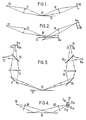
- the means comprise a source 10 of monochromatic light associated with a lens 11 which forms from the source an image 12 which is on the surface of the wafer 13 when the latter is in its nominal position, as indicated in FIG. 1.
- Means of light recovery shown schematically in the form of a lens 14, form of the spot of light on the surface 13 an image which, when the wafer 13 is in its nominal position, is centered relative to a differential photodetector 15, which may in particular be constituted either by a diode with two quadrants, or by two separate diodes. There is thus obtained by difference an error signal which is introduced into a control loop.
- any offset in altitude ⁇ z of the section 13 causes an offset ⁇ x of the image on the differential photodetector 15, therefore an error signal which is an increasing function of ⁇ x and whose sign depends on the direction of ⁇ z.
- Such an autofocus device can be very sensitive, especially if it uses a very oblique angle. But it has a serious drawback.
- An irregularity in the reflection of the surface of the wafer 13 causes an asymmetry in the intensity distribution of the spot and can lead to a focusing error.
- the means of detection of the deviations then comprise a source, for example a laser diode, an optic for focusing the light emitted in the form of a spot, an optic comprising a mirror for picking up the reflected light and returning it along a path opposite to the outward path to a deviation detector.
- the invention aims to provide a projection device of the type defined above, meeting better than those previously known the requirements of practice, in particular in that it comprises an automatic focusing device making it possible to simply spread problems related to image surface reflection defects.
- the invention proposes in particular an apparatus in which two sets of said means are provided, corresponding to reverse paths of the light, and means for summing the differential signals supplied by the two photodetectors.
- the automatic focusing device advantageously further comprises means for detecting angular deviations, that is to say in attitude, between the image surface and a nominal position.
- These means may in particular comprise a source for illuminating the surface by a parallel beam in oblique incidence and means for focusing the image of the source on a four-quadrant photodetector, the grouping of the output signals of the four quadrants allowing to obtain attitude error signals around two perpendicular axes.
- the invention also aims to solve a particular problem in the case of photorepeaters.
- graticule inspection apparatuses are known by photometric comparison of two homologous zones of adjacent patterns. But this solution has many disadvantages. It is indeed the crosshair that we control, and not the image of the crosshair in the plane of the slice. And, in addition, there is a risk of dust being deposited during the transfer between the recording equipment and the photorepeater.
- the invention also aims to eliminate this drawback. To this end, it proposes a projection device constituting a photorepeater, comprising means for forming two homologous zones of adjacent patterns on two photoelectric detectors and for measuring the difference in output signals of the two detectors.
- This solution is applicable whenever several elementary integrated circuit patterns appear on the same reticle, which is frequently the case since this thus reduces the duration of photorepetition on a wafer.
- the actual image is examined directly and not the reticle, which makes it possible to take into account only the defects likely to be actually printed on the silicon wafer and to accept reticles which would be rejected on a conventional inspection device.
- the fault detection resolution is of the same order as the resolution of the objective, that is to say equal to or even less than one micron.
- the various components of the device can occupy very different positions relative to those which are used directly for projection.
- the angular deviation detection means can use a light path making an angle, for example a right angle, with the light paths in said sets of means.
- the first set (in which the elements corresponding to those in FIG. 1 are designated by the same reference number) comprises a monochromatic light source 10 whose output beam is collected by a semi-transparent plate 16 whose role will appear more far.
- the beam reflected by this blade is focused by a lens 11 and a deflection mirror 17 in a spot 12 which is on the surface of the wafer 13 when the latter occupies its nominal position.
- a mirror 17a symmetrical to the mirror 17 and a lens 14 symmetrical to the lens 11 refocus the spot 12 on a differential photodetector 15 through a semi-transparent plate 16a.
- a system comprising the semi-transparent plate 16a, the lens 14 and the mirror 17a forms from the source 10a an image merged with the spot 12.
- the light reflected by the surface 13 is taken up by the mirror 17, the lens 11 and the semi-transparent plate 16 for forming an image on a photodetector 15a similar to the photodetector 15.
- the error signal will be:
- the detectors will obviously be placed and adjusted so that the output signal, which can be produced by a conventional analog adder circuit, is zero when the surface 13 occupies its nominal position.
- the problem encountered in the case of a single passage of light is eliminated: in fact, the image of an asymmetric spot on the photodetector 15 will also be asymmetrical in the same way on the photodetector 15a. Furthermore, the sources 10 and 10a can without drawback have slightly different intensities, because the average of the two photoelectric signals is used.
- photorepeaters generally include an automatic focusing device, but which only ensures the correction of deviations in altitude.
- the present invention makes it possible to easily carry out a control of adjustment in trim, the interest of which has so far not been appreciated.
- an automatic focusing in plate is extremely desirable, because it alone makes it possible to correct slow defects in flatness of the silicon wafers.
- FIGS. 4 and 5 show means for detecting difference in attitude which can be incorporated in a projection apparatus to supply, to a focusing device, the input signals necessary for adjustment in attitude.
- the means shown in FIGS. 4 and 5 comprise means making it possible to send, on edge 13, a monochromatic parallel light beam, in oblique incidence.
- These means comprise a source 18 and an optic shown diagrammatically by a lens 19.
- a second optic also shown diagrammatically by a lens 20, focuses the image of the source point 18 on a quadruple photodetector 21 which can be formed by. a diode with four quadrants D 11 ' D 12 , D 13 and D 14 .
- an offset in attitude ⁇ around an axis perpendicular to the plane of the figure results in an offset ⁇ x on the photodetector 21. If we denote by D 11 , D 12 , D 13 and D 14 the output signals of the four quadrants, the corresponding error signal will be:
- Error signals can be injected into servo loops at ⁇ and ⁇ . These loops will not be described here, any more than the mechanical devices for correct positioning, since they can be of a conventional type, such as for example that described in "The Bell System Technical Journal", November 1970, pp. 2158.2160.
- the means for detecting deviation in altitude and in attitude can be located around the objective of the same photorepeater, as shown in FIGS. 6 and 7; the optical paths of the difference in altitude and attitude measurement means are crossed and the paths frame the objective 22.
- the sources 15, 15a and 18 can be constituted by independent emitters but of sufficient intensity (laser diode for example ) or by the terminal parts of optical fibers.
- the return mirrors 17 and 17a as well as the semi-transparent blades 16 and 16a are formed by prisms.
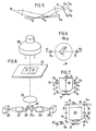
- FIG. 7A where the members corresponding to those of FIG. 7 are designated by the same reference number, a single source 10 is used for the focus and trim checks.
- the parallel light brush coming from the source 10 is divided by a semi-transparent separating blade 30 into a reflected beam which follows a first path and a transmitted brush whose part reflected by a second separating blade 31 follows a second path, symmetrical with the first when the surface 13 of the silicon wafer has a correct attitude.
- the source points are constituted by respective diaphragms 35 and 35a, the image of which is formed, respectively by the lenses 11 and 11a, on the surface 13.
- the two p hotodetectors 15 and 15a collect the light coming from the wafer 13 and transmitted respectively through the blades 30 and 31.
- the attitude control uses a fraction of the brush which returns to the photodetector 15a, a fraction sampled by reflection on a semi-transparent separating plate 32 and returned to the photodetector 21, generally constituted by a diode with four quadrants. This diode is located at the focal point of the lens 11.
- FIG. 8 schematically shows the reduction objective 22 of the photorepeater which makes it possible to form, from the object reticle 23, once the latter in place in the photorepeater, a real aerial image 24. Inspection and verification are carried out by comparison between the homologous areas of two adjacent patterns, which does not constitute a real limitation, because reasons of speed generally lead to exposing several patterns at the same time. It may be noted in passing that the useful field of a photorepeater is generally of the order of 1 cm ⁇ 1 cm and that the invention will therefore be usable each time the unit dimension of each pattern does not exceed 0.5 cm, which is the most common case.
- the inspection means comprise two mirrors or, as illustrated in FIG. 8, two total reflection prisms 25 and 25a in the form of a half-cube. These two prisms send two homologous images of a small surface of the integrated circuit onto two photosensitive detectors 26 and 26a via two microscope objectives 27 and 27a. All of these elements can constitute a very compact unit, housed near the silicon wafer, on a support secured to the xy table which carries the wafer.
- the signals measured by the photodetectors 26 and 26a are different if the homologous surfaces, delimited by circles in FIG. 8, do not have the same transmission. The difference between the two signals indicates the presence of an opaque or transparent defect in one of the two images.
- each photoelectric detector 26 and 26a will correspond for example to a rectangle of 1 x 5 microns or of 1 x 10 microns. It is thus possible to analyze the image of the reticle by scanning of the television type, by successive lines, 5 microns or 10 microns wide. The complete comparison operation between two circuits of 5 x 5 mm therefore leads to scanning 1000 lines of width 5 microns and length 5 mm, ie a total travel of the table of 5 m. The total control time will therefore only be 100 seconds if the movement is made at an average speed of 5 cm / s. We see that we do not significantly reduce the speed of the photorepeater due to the inspection of the reticle before exposing one or more batches of slices.
- the means shown in FIG. 8 can be saved with their position in memory of a minicomputer which, at the end of the check, provides the map of the circuit. This image of the circuit helps to find the fault under a microscope and to make it disappear, if possible, for example if it is a dust. It is not necessary to describe here the means of recording in memory, since they can be conventional.
Description
La présente invention a pour objet un appareil de projection sur une surface image à l'aide d'une optique du type comportant un dispositif de mise au point muni d'un jeu de moyens de détection des écarts entre la surface image et une position nominale par rapport à l'optique, ce jeu ayant des moyens solidaires de l'optique pour former, sur ladite surface, une tache de lumière monochromatique en incidence oblique et des moyens de reprise de la lumière provenant de ladite surface pour former de la tache une image qui est centrée sur un photodétecteur différentiel lorsque la surface occupe sa position nominale par rapport à l'optique.The present invention relates to an apparatus for projecting onto an image surface using an optical system of the type comprising a focusing device provided with a set of means for detecting deviations between the image surface and a nominal position. with respect to the optics, this game having means integral with the optics for forming, on said surface, a spot of monochromatic light in oblique incidence and means for recovering the light coming from said surface to form a spot image which is centered on a differential photodetector when the surface occupies its nominal position relative to the optics.
L'invention trouve une application particulièrement importante dans les appareils utilisés pour la fabrication des circuits intégrés, et notamment dans ceux, connus sous le nom de « photorépéteurs sur tranche », destinés à former de façon répétitive l'image d'un réticule ou masque dans des zones successives de la surface d'une tranche de semi-conducteur.The invention finds a particularly important application in the apparatuses used for the manufacture of integrated circuits, and in particular in those, known under the name of "photorepeaters on edge", intended to form in a repetitive way the image of a reticle or mask in successive areas of the surface of a semiconductor wafer.
Il est nécessaire de maintenir la distance entre l'optique, qui constitue l'objectif du photorépéteur, et la surface image sous peine de dégradation de celle-ci. A titre d'exemple, on peut mentionner que la distance entre objectif et surface image est de 6 mm sur un photorépéteur commercial actuel et que la tolérance est alors de 2 microns pour projeter des traits dont la largeur est de 1 micron.It is necessary to maintain the distance between the optics, which constitutes the objective of the photorepeater, and the image surface on pain of degradation of the latter. As an example, we can mention that the distance between objective and image surface is 6 mm on a current commercial photorepeater and that the tolerance is then 2 microns to project lines whose width is 1 micron.
On connaît déjà des appareils de projection constituant photorépéteur du type ci-dessus défini, dont le dispositif de mise au point fonctionne de façon automatique. Un tel dispositif existe par exemple sur les photorépéteurs fabriqués par la société G.C.A. depuis 1977 au moins., La constitution et le fonctionnement de principe des moyens de détection sont illustrés sur les figures 1 et 2 ci-jointes. Les moyens comprennent une source 10 de lumière monochromatique associée à une lentille 11 qui forme de la source une image 12 qui se trouve sur la surface de la tranche 13 lorsque cette dernière est dans sa position nominale, comme indiqué sur la figure 1. Des moyens de reprise de la lumière, schématisés sous forme d'une lentille 14, forment de la tache de lumière sur la surface 13 une image qui, lorsque la tranche 13 est dans sa position nominale, est centrée par rapport à un photodétecteur différentiel 15, qui peut notamment être constitué soit par une diode à deux quadrants, soit par deux diodes séparées. On obtient ainsi par différence un signal d'erreur que l'on introduit dans une boucle d'asservissement.There are already known projection apparatuses constituting a photorepeater of the type defined above, the focusing device of which operates automatically. Such a device exists for example on photorepeaters produced by the company G.C.A. since at least 1977., The constitution and the principle functioning of the detection means are illustrated in FIGS. 1 and 2 attached. The means comprise a
Comme le montre la Figure 2, tout décalage en altitude Δz de la tranche 13 provoque un décalage Δx de l'image sur le photodétecteur différentiel 15, donc un signal d'erreur qui est une fonction croissante de Δx et dont le signe dépend du sens de Δz.As shown in FIG. 2, any offset in altitude Δz of the
Un tel dispositif de mise au point automatique peut être très sensible, surtout s'il utilise une incidence très oblique. Mais il présente un inconvénient grave. Une irrégularité de réflexion de la surface de la tranche 13 entraîne une asymétrie dans la répartition d'intensité de la tache et peut entraîner une erreur de mise au point.Such an autofocus device can be very sensitive, especially if it uses a very oblique angle. But it has a serious drawback. An irregularity in the reflection of the surface of the
On a tenté d'écarter cette difficulté en obligeant la lumière à suivre le même trajet dans un sens, puis dans l'autre, en remplaçant le photodétecteur 15 par un miroir de retour vers un détecteur placé à proximité de la source 10. Les moyens de détection des écarts comportent alors une source, par exemple une diode laser, une optique pour focaliser la lumière émise sous forme d'une tache, une optique comportant un miroir pour reprendre la lumière réfléchie et la renvoyer suivant un trajet opposé au trajet aller vers un détecteur d'écart. Cette solution, décrite notamment dans « Solid State Technology •, juin 1980, pp. 80-84 et dans le document GB-A-2 052 090, est celle qui vient immédiatement à l'esprit. Mais elle n'est pas satisfaisante car le faisceau de retour a une intensité beaucoup plus faible que le faisceau aller, par suite des pertes d'absorption et de diffusion qui sont particulièrement importantes du fait de la grande incidence que doivent avoir les faisceaux sur la surface image. Les irrégularités de réflexion éventuelles de la surface image ne sont en conséquence nullement compensées. Cette solution n'est donc pas satisfaisante, car elle n'assure pas les compensations requises dans les conditions pratiques d'utilisation.We tried to avoid this difficulty by forcing the light to follow the same path in one direction, then in the other, by replacing the
L'invention vise à fournir un appareil de projection du type ci-dessus défini, répondant mieux que ceux antérieurement connus aux exigences de la pratique, notamment en ce qu'il comporte un dispositif de mise au point automatique permettant d'écarter de façon simple les problèmes liés aux défauts de réflexion de la surface image.The invention aims to provide a projection device of the type defined above, meeting better than those previously known the requirements of practice, in particular in that it comprises an automatic focusing device making it possible to simply spread problems related to image surface reflection defects.
Dans ce but, l'invention propose notamment un appareil dans lequel sont prévus deux jeux desdits moyens, correspondant à des trajets inverses de la lumière, et des moyens pour faire la somme des signaux différentiels fournis par les deux photodétecteurs.To this end, the invention proposes in particular an apparatus in which two sets of said means are provided, corresponding to reverse paths of the light, and means for summing the differential signals supplied by the two photodetectors.
Pour permettre de disposer de jeux de moyens correspondant à des trajets inverses, on utilisera en général des lames semi-transparentes de renvoi de lumière provenant de la source de l'un des jeux et de transmission de la lumière vers le photodétecteur de l'autre jeu.To allow sets of means corresponding to reverse paths to be available, semi-transparent slats for returning light from the source of one of the sets and for transmitting light to the photodetector of the other will generally be used. Game.
Le dispositif de mise au point automatique comporte avantageusement de plus des moyens de détection des écarts angulaires, c'est-à-dire en assiette, entre la surface image et une position nominale. Ces moyens peuvent notamment comporter une source pour éclairer la surface par un faisceau parallèle en incidence oblique et des moyens pour focaliser l'image de la source sur un photodétecteur à quatre quadrants, le groupement des signaux de sortie des quatre quadrants permettant d'obtenir des signaux d'erreur en assiette autour de deux axes perpendiculaires.The automatic focusing device advantageously further comprises means for detecting angular deviations, that is to say in attitude, between the image surface and a nominal position. These means may in particular comprise a source for illuminating the surface by a parallel beam in oblique incidence and means for focusing the image of the source on a four-quadrant photodetector, the grouping of the output signals of the four quadrants allowing to obtain attitude error signals around two perpendicular axes.
Enfin, l'invention vise par ailleurs à résoudre un problème particulier au cas des photorépéteurs. Quand on manipule des réticules ou masques en vue de les impressionner en plusieurs zones successives sur une tranche de semiconducteur, il est nécessaire de prendre des précautions pour éviter le dépôt sur ces réticules de particules dont l'image serait reproduite sur le circuit intégré. A l'heure actuelle, on connaît des appareils d'inspection de réticule par comparaison photométrique de deux zones homologues de motifs adjacents. Mais cette solution a de nombreux inconvénients. C'est en effet le réticule que l'on contrôle, et non pas l'image du réticule dans le plan de la tranche. Et, de plus, il existe un risque que des poussières se déposent pendant le transfert entre l'appareil de contrôle et le photorépéteur.Finally, the invention also aims to solve a particular problem in the case of photorepeaters. When handling reticles or masks in order to impress them in several successive zones on a semiconductor wafer, it is necessary to take precautions to avoid the deposition on these reticles of particles whose image would be reproduced on the integrated circuit. At the present time, graticule inspection apparatuses are known by photometric comparison of two homologous zones of adjacent patterns. But this solution has many disadvantages. It is indeed the crosshair that we control, and not the image of the crosshair in the plane of the slice. And, in addition, there is a risk of dust being deposited during the transfer between the recording equipment and the photorepeater.
L'invention vise également à écarter cet inconvénient. Dans ce but, elle propose un appareil de projection constituant photorépéteur, comprenant des moyens de formation de deux zones homologues de motifs adjacents sur deux détecteurs photoélectriques et de mesure de la différence de signaux de sortie des deux détecteurs.The invention also aims to eliminate this drawback. To this end, it proposes a projection device constituting a photorepeater, comprising means for forming two homologous zones of adjacent patterns on two photoelectric detectors and for measuring the difference in output signals of the two detectors.
Cette solution est applicable chaque fois que plusieurs motifs élémentaires de circuit intégré figurent sur un même réticule, ce qui est fréquem- ment le cas étant donné que l'on réduit ainsi la durée de photorépétition sur tranche. On examine directement l'image réelle et non pas le réticule, ce qui permet de ne tenir compte que des défauts susceptibles d'être imprimés effectivement sur la tranche de silicium et d'accepter des réticules qui seraient rejetés sur un appareil classique d'inspection. La résolution de détection de défaut est du même ordre que la résolution de l'objectif, c'est-à-dire égale ou même inférieure au micron.This solution is applicable whenever several elementary integrated circuit patterns appear on the same reticle, which is frequently the case since this thus reduces the duration of photorepetition on a wafer. The actual image is examined directly and not the reticle, which makes it possible to take into account only the defects likely to be actually printed on the silicon wafer and to accept reticles which would be rejected on a conventional inspection device. . The fault detection resolution is of the same order as the resolution of the objective, that is to say equal to or even less than one micron.
Les différents composants du dispositif peuvent occuper des positions très diverses par rapport à ceux qui servent directement à la projection. Par exemple, les moyens de détection d'écart angulaire peuvent utiliser un trajet de lumière faisant un angle, par exemple droit, avec les trajets de lumière dans lesdits jeux de moyens.The various components of the device can occupy very different positions relative to those which are used directly for projection. For example, the angular deviation detection means can use a light path making an angle, for example a right angle, with the light paths in said sets of means.
L'invention sera mieux comprise à la lecture de la description qui suit de modes particuliers de mise en oeuvre de l'invention, donnés à titre d'exemples non limitatifs. La description se réfère aux dessins qui l'accompagnent, dans lesquels :
- les figures 1 et 2 sont des schémas de principe montrant un jeu de moyens de détection d'écart suivant l'art antérieur, respectivement lorsque la surface image est dans sa position nominale et lorsqu'elle en est écartée ;
- la figure 3 est un schéma de principe, similaire à la figure 1, montrant l'ensemble des moyens de détection d'un appareil suivant un premier mode de réalisation de l'invention, dans lequel seuls sont détectés les écarts en altitude ;
- les figures 4 et 5 sont des schémas de principe similaires aux figures 1 et 2, montrant des moyens pouvant être associés à ceux de la figure 3 et permettant une détection des écarts angulaires, c'est-à-dire en assiette ;
- la figure 6 est un schéma en plan, montrant la répartition et la constitution des photodétecteurs de moyens de détection des écarts en altitude et en assiette ;
- la figure 7 est un schéma d'implantation des moyens dans un photorépéteur ;
- la figure 7A montre une variante de la figure 7 ;
- la figure 8 est un schéma de principe, en perspective, montrant l'implantation de moyens d'inspection de réticule pour appareil de projection constituant photorépéteur.
- Figures 1 and 2 are block diagrams showing a set of deviation detection means according to the prior art, respectively when the image surface is in its nominal position and when it is moved away from it;
- Figure 3 is a block diagram, similar to Figure 1, showing all of the detection means of an apparatus according to a first embodiment of the invention, in which only differences in altitude are detected;
- Figures 4 and 5 are block diagrams similar to Figures 1 and 2, showing means which can be associated with those of Figure 3 and allowing detection of angular deviations, that is to say in attitude;
- FIG. 6 is a plan diagram, showing the distribution and constitution of the photodetectors of means for detecting deviations in altitude and in attitude;
- Figure 7 is a layout diagram of the means in a photorepeater;
- Figure 7A shows a variant of Figure 7;
- Figure 8 is a block diagram, in perspective, showing the establishment of reticle inspection means for projection apparatus constituting photorepeater.
On décrira tout d'abord, en faisant référence à la figure 3, les moyens de détection des écarts en altitude entre la surface image 13, constituée par une tranche de silicium susceptible de présenter des défauts d'épaisseur et de planéité, et une position de référence.We will first describe, with reference to Figure 3, the means for detecting differences in altitude between the
Ces moyens sont entièrement symétriques et peuvent être regardés comme comportant deux jeux de moyens identiques. Le premier jeu (sur lequel les éléments correspondant à ceux de la figure 1 sont désignés par le même numéro de référence) comprend une source de lumière monochromatique 10 dont le faisceau de sortie est recueilli par une lame semi-transparente 16 dont le rôle apparaîtra plus loin. Le faisceau réfléchi par cette lame est focalisé par une lentille 11 et un miroir de renvoi 17 en une tache 12 qui se trouve sur la surface de la tranche 13 lorsque celle-ci occupe sa position nominale. Un miroir 17a symétrique du miroir 17 et une lentille 14 symétrique de la lentille 11 refocalisent la tache 12 sur un photodétecteur différentiel 15 à travers une lame semi-transparente 16a. Symétriquement, un système comportant la lame semi-transparente 16a, la lentille 14 et le miroir 17a forme de la source 10a une image confondue avec la tache 12. La lumière réfléchie par la surface 13 est reprise par le miroir 17, la lentille 11 et la lame semi-transparente 16 pour former une image sur un photodétecteur 15a similaire au photodétecteur 15.These means are entirely symmetrical and can be viewed as comprising two sets of identical means. The first set (in which the elements corresponding to those in FIG. 1 are designated by the same reference number) comprises a
Si l'on suppose que les photodétecteurs 15 et 15a comportent chacun deux quadrants, respectivement D1 et D2, D1a et D2a, le signal d'erreur sera :![]()
![]()
Les détecteurs seront évidemment placés et ajustés de façon que le signal de sortie, qui peut être élaboré par un circuit analogique additionneur classique, soit nul lorsque la surface 13 occupe sa position nominale.The detectors will obviously be placed and adjusted so that the output signal, which can be produced by a conventional analog adder circuit, is zero when the
Grâce à cette disposition, on élimine le problème rencontré en cas d'un seul passage de lumière : en effet, l'image d'une tache asymétrique sur le photodétecteur 15 sera également asymétrique de la même manière sur le photodétecteur 15a. Par ailleurs, les sources 10 et 10a peuvent sans inconvénient avoir des intensités légèrement différentes, car on utilise la moyenne des deux signaux photoélectriques.Thanks to this arrangement, the problem encountered in the case of a single passage of light is eliminated: in fact, the image of an asymmetric spot on the
A l'heure actuelle, les photorépéteurs comportent en général un dispositif de mise au point automatique, mais qui n'assure que la correction des écarts en altitude. La présente invention permet de réaliser aisément un contrôle de mise au point en assiette dont, jusqu'à présent, l'intérêt n'a pas été apprécié. En fait, une mise au point automatique en assiette est extrêmement souhaitable, car elle seule permet de corriger des défauts lents de planéité des tranches de silicium.At present, photorepeaters generally include an automatic focusing device, but which only ensures the correction of deviations in altitude. The present invention makes it possible to easily carry out a control of adjustment in trim, the interest of which has so far not been appreciated. In fact, an automatic focusing in plate is extremely desirable, because it alone makes it possible to correct slow defects in flatness of the silicon wafers.
Les figures 4 et 5 montrent des moyens de détection d'écart en assiette qui peuvent être incorporés dans un appareil de projection pour fournir, à un dispositif de mise au point, les signaux d'entrée nécessaires à un réglage en assiette.FIGS. 4 and 5 show means for detecting difference in attitude which can be incorporated in a projection apparatus to supply, to a focusing device, the input signals necessary for adjustment in attitude.
Les moyens montrés en figures 4 et 5 comprennent des moyens permettant d'envoyer, sur la tranche 13, un faisceau de lumière parallèle monochromatique, en incidence oblique. Ces moyens comprennent une source 18 et une optique schématisée par une lentille 19. Une seconde optique, également schématisée par une lentille 20, focalise l'image du point source 18 sur un photodétecteur quadruple 21 qui peut être constitué par. une diode à quatre quadrants D11' D12, D13 et D14. Comme le montre la figure 5, un décalage en assiette Δφ autour d'un axe perpendiculaire au plan de la figure se traduit par un décalage Δx sur le photodétecteur 21. Si l'on désigne par D11, D12, D13 et D14 les signaux de sortie des quatre quadrants, le signal d'erreur correspondant sera :![]()
![]()
De façon similaire, tout décalage ΔΨ en assiette autour d'un axe parallèle au plan de la figure se traduira par un signal d'erreur :![]()
![]()
Les signaux d'erreur peuvent être injectés dans des boucles d'asservissement en ϕ et Ψ. On ne décrira pas ici ces boucles, pas plus que les dispositifs mécaniques de remise en position correcte, car elles peuvent être d'un type classique, tel par exemple que celui décrit dans « The Bell System Technical Journal », novembre 1970, pp. 2158.2160.Error signals can be injected into servo loops at ϕ and Ψ. These loops will not be described here, any more than the mechanical devices for correct positioning, since they can be of a conventional type, such as for example that described in "The Bell System Technical Journal", November 1970, pp. 2158.2160.
Il faut remarquer qu'un double passage de lumière suivant deux trajets opposés n'est pas nécessaire ici, car la refocalisation sur le photodétecteur s'accompagne d'une détermination de valeur moyenne.It should be noted that a double passage of light following two opposite paths is not necessary here, since the refocusing on the photodetector is accompanied by a determination of average value.
Les moyens de détection d'écart en altitude et en assiette peuvent être situés autour de l'objectif d'un même photorépéteur, comme le montrent les figures 6 et 7 ; les trajets optiques des moyens de mesure d'écart en altitude et en assiette sont croisés et les trajets encadrent l'objectif 22. Les sources 15, 15a et 18 peuvent être constituées par des émetteurs indépendants mais d'intensité suffisante (diode laser par exemple) ou par les parties terminales de fibres optiques. Les miroirs de renvoi 17 et 17a ainsi que les lames semi-transparentes 16 et 16a sont constitués par des prismes.The means for detecting deviation in altitude and in attitude can be located around the objective of the same photorepeater, as shown in FIGS. 6 and 7; the optical paths of the difference in altitude and attitude measurement means are crossed and the paths frame the objective 22. The
En utilisant les lentilles 11 et 11a de focale 50 mm et un grandissement de dix, un défaut de mise au point en altitude Δz = 2 microns donne un déplacement du spot qui est approximativement de 40 microns. Un défaut d'assiette Δϕ = 5 microns/cm donnera, pour une focale de 50 mm, un déplacement du spot égal à 50 microns environ.Using the
On voit que de tels déplacements sont aisément décelables à l'aide de photodétecteurs courants.It can be seen that such displacements are easily detectable using standard photodetectors.
Dans la variante de réalisation montrée en figure 7A, où les organes correspondant à ceux de la figure 7 sont désignés par le même numéro de référence, on utilise une seule source 10 pour les contrôles de mise au point et d'assiette.In the alternative embodiment shown in FIG. 7A, where the members corresponding to those of FIG. 7 are designated by the same reference number, a
Le pinceau de lumière parallèle provenant de la source 10 (laser He-Ne par exemple) est fractionné par une lame séparatrice semi-transparente 30 en un faisceau réfléchi qui suit un premier trajet et un pinceau transmis dont la partie réfléchie par une seconde lame séparatrice 31 suit un second trajet, symétrique de premier lorsque la surface 13 de la tranche de silicium présente une assiette correcte. Les points sources sont constitués par des diaphragmes respectifs 35 et 35a dont l'image est formée, respectivement par les lentilles 11 et 11a, sur la surface 13. Les deux photodétecteurs différentiels 15 et 15a recueillent la lumière provenant de la tranche 13 et transmise respectivement à travers les lames 30 et 31.The parallel light brush coming from the source 10 (He-Ne laser for example) is divided by a
Le contrôle d'assiette utilise une fraction du pinceau qui revient vers le photodétecteur 15a, fraction prélevée par réflexion sur une lame séparatrice semi-transparente 32 et renvoyée vers le photodétecteur 21, constitué en général par une diode à quatre quadrants. Cette diode est située au foyer de la lentille 11.The attitude control uses a fraction of the brush which returns to the
Ce système représente une simplification notable du précédent.This system represents a notable simplification of the previous one.
On décrira maintenant, en faisant référence à la figure 8, des moyens d'inspection de l'image du réticule qui peuvent être incorporés à un photorépéteur comprenant par ailleurs un dispositif de mise au point automatique du genre qui a été décrit plus haut.A description will now be given, with reference to FIG. 8, of means for inspecting the image of the reticle which can be incorporated into a photorepeater, moreover comprising an automatic focusing device of the kind which has been described above.
La figure 8 montre schématiquement l'objectif de réduction 22 du photorépéteur qui permet de former, du réticule objet 23, une fois ce dernier en place dans le photorépéteur, une image réelle aérienne 24. L'inspection et la vérification s'effectuent par comparaison entre les zones homologues de deux motifs adjacents, ce qui ne constitue pas une limitatiion réelle, car des raisons de rapidité conduisent généralement à exposer plusieurs motifs à la fois. On peut noter au passage que le champ utile d'un photorépéteur est généralement de l'ordre de 1 cm x 1 cm et que l'invention sera donc utilisable chaque fois que la dimension unitaire de chaque motif ne dépasse pas 0,5 cm, ce qui est le cas le plus fréquent.FIG. 8 schematically shows the
Les moyens d'inspection comprennent deux miroirs ou, comme illustré sur la figure 8, deux prismes à réflexion totale 25 et 25a en forme de demi-cube. Ces deux prismes envoient deux images homologues d'une petite surface du circuit intégré sur deux détecteurs photosensibles 26 et 26a par l'intermédiaire de deux objectifs de microscopes 27 et 27a. L'ensemble de ces éléments peut constituer un ensemble très compact, logé près de'la tranche de silicium, sur un support solidarisé de la table xy qui porte la tranche.The inspection means comprise two mirrors or, as illustrated in FIG. 8, two
Lorsque l'illuminateur 28 est allumé et provoque la formation des images montrées en tirets en 24, les signaux mesurés par les photodétecteurs 26 et 26a sont différents si les surfaces homologues, délimitées par des cercles sur la figure 8, n'ont pas la même transmission. La différence entre les deux signaux signale la présence d'un défaut opaque ou transparent sur l'une des deux images.When the
La surface vue par chaque détecteur photoé- lectrique 26 et 26a correspondra par exemple à un rectangle de 1 x 5 microns ou de 1 x 10 microns. On peut ainsi analyser l'image du réticule par balayage du type télévision, par lignes successives, larges de 5 microns ou 10 microns. L'opération complète de comparaison entre deux circuits de 5 x 5 mm conduit donc à balayer 1 000 lignes de largeur 5 microns et de longueur 5 mm, soit un parcours total de la table de 5 m. Le temps total de contrôle ne sera donc que de 100 secondes si le déplacement se fait à une vitesse moyenne de 5 cm/s. On voit que l'on ne réduit pas sensiblement le débit du photorépéteur du fait de l'inspection du réticule avant d'exposer un ou plusieurs lots de tranches.The surface seen by each
Les moyens montrés en figure 8 peuvent être enregistrés avec leur position en mémoire d'un minicalculateur qui, en fin de contrôle, fournit la cartographie du circuit. Cette image du circuit aide à retrouver le défaut sous microscope et à le faire disparaître, si cela est possible, par exemple s'il s'agit d'une poussière. Il n'est pas nécessaire de décrire ici les moyens d'enregistrement en mémoire, étant donné qu'ils peuvent être classiques.The means shown in FIG. 8 can be saved with their position in memory of a minicomputer which, at the end of the check, provides the map of the circuit. This image of the circuit helps to find the fault under a microscope and to make it disappear, if possible, for example if it is a dust. It is not necessary to describe here the means of recording in memory, since they can be conventional.
Claims (6)
Applications Claiming Priority (2)
| Application Number | Priority Date | Filing Date | Title |
|---|---|---|---|
| FR8107709 | 1981-04-16 | ||
| FR8107709A FR2504281A1 (en) | 1981-04-16 | 1981-04-16 | PROJECTION APPARATUS WITH FOCUSING DEVICE |
Publications (2)
| Publication Number | Publication Date |
|---|---|
| EP0063980A1 EP0063980A1 (en) | 1982-11-03 |
| EP0063980B1 true EP0063980B1 (en) | 1985-06-26 |
Family
ID=9257505
Family Applications (1)
| Application Number | Title | Priority Date | Filing Date |
|---|---|---|---|
| EP82400636A Expired EP0063980B1 (en) | 1981-04-16 | 1982-04-06 | Projection apparatus with a focusing device |
Country Status (5)
| Country | Link |
|---|---|
| US (1) | US4477185A (en) |
| EP (1) | EP0063980B1 (en) |
| JP (1) | JPS57188027A (en) |
| DE (1) | DE3264399D1 (en) |
| FR (1) | FR2504281A1 (en) |
Families Citing this family (25)
| Publication number | Priority date | Publication date | Assignee | Title |
|---|---|---|---|---|
| JPS58113706A (en) * | 1981-12-26 | 1983-07-06 | Nippon Kogaku Kk <Nikon> | Detector for horizontal position |
| JPS59121932A (en) * | 1982-12-28 | 1984-07-14 | Fujitsu Ltd | Automatic focusing control unit |
| US4845373A (en) * | 1984-02-22 | 1989-07-04 | Kla Instruments Corporation | Automatic alignment apparatus having low and high resolution optics for coarse and fine adjusting |
| NL8401710A (en) * | 1984-05-29 | 1985-12-16 | Philips Nv | DEVICE FOR IMAGING A MASK PATTERN ON A SUBSTRATE. |
| FR2580087B1 (en) * | 1985-04-03 | 1988-12-02 | Hispano Suiza Sa | |
| US4810077A (en) * | 1986-02-13 | 1989-03-07 | Spectra-Tech, Inc. | Grazing angle microscope |
| US4721386A (en) * | 1986-07-18 | 1988-01-26 | Barnes Engineering Company | Three-axis angular monitoring system |
| US4821196A (en) * | 1987-02-20 | 1989-04-11 | International Business Machines Corporation | High resolution automatic focus correction electronic subsystem for E-beam lithography |
| US4886958A (en) * | 1988-03-25 | 1989-12-12 | Texas Instruments Incorporated | Autofocus system for scanning laser inspector or writer |
| DE3921661C1 (en) * | 1989-06-30 | 1991-01-17 | Fraunhofer-Gesellschaft Zur Foerderung Der Angewandten Forschung Ev, 8000 Muenchen, De | |
| FR2674036B1 (en) * | 1991-03-13 | 1993-07-30 | Mrejen Jean Jacques | METHOD FOR CONTROLLING FOCUS FOR SHOOTING AND ORDERING MEMBER THEREFOR. |
| EP0505717B1 (en) * | 1991-03-25 | 1998-07-29 | Heidelberger Druckmaschinen Aktiengesellschaft | Method and apparatus for optically measuring distance |
| JP2943499B2 (en) * | 1992-04-22 | 1999-08-30 | 日本電気株式会社 | Height measuring method and device |
| US5311288A (en) * | 1992-07-06 | 1994-05-10 | Opal Technologies Ltd. | Method and apparatus for detecting surface deviations from a reference plane |
| US5510892A (en) * | 1992-11-25 | 1996-04-23 | Nikon Corporation | Inclination detecting apparatus and method |
| US5636013A (en) * | 1995-01-04 | 1997-06-03 | Hutchinson Technology Incorporated | Suspension assembly static attitude and distance measuring instrument |
| US6166808A (en) * | 1996-12-24 | 2000-12-26 | U.S. Philips Corporation | Optical height meter, surface-inspection device provided with such a height meter, and lithographic apparatus provided with the inspection device |
| US5844727A (en) * | 1997-09-02 | 1998-12-01 | Cymer, Inc. | Illumination design for scanning microlithography systems |
| US6774945B1 (en) * | 1999-10-18 | 2004-08-10 | Hewlett-Packard Development Company, L.P. | Focusing apparatus for image recording system |
| DE10026830A1 (en) * | 2000-05-30 | 2001-12-06 | Zeiss Carl Jena Gmbh | Optical sensor for measuring the distance and / or the inclination of a surface |
| DE10233087A1 (en) * | 2002-07-19 | 2004-02-05 | Roche Diagnostics Gmbh | Reflection photometric analysis system |
| US9310598B2 (en) * | 2009-03-11 | 2016-04-12 | Sakura Finetek U.S.A., Inc. | Autofocus method and autofocus device |
| DE102013103971A1 (en) | 2013-04-19 | 2014-11-06 | Sensovation Ag | Method for generating an overall picture of an object composed of several partial images |
| US10007102B2 (en) | 2013-12-23 | 2018-06-26 | Sakura Finetek U.S.A., Inc. | Microscope with slide clamping assembly |
| US11280803B2 (en) | 2016-11-22 | 2022-03-22 | Sakura Finetek U.S.A., Inc. | Slide management system |
Family Cites Families (14)
| Publication number | Priority date | Publication date | Assignee | Title |
|---|---|---|---|---|
| US3517992A (en) * | 1968-04-24 | 1970-06-30 | Leitz Ernst Gmbh | Automatic focusing slide projector |
| US3612698A (en) * | 1969-05-01 | 1971-10-12 | Ibm | Automatic holographic wafer positioning system and method |
| GB1312663A (en) * | 1970-05-28 | 1973-04-04 | Ti Group Services Ltd | Optical control means |
| US3645623A (en) * | 1970-09-25 | 1972-02-29 | Raymond A Patten | Apparatus for monitoring film thickness by reflecting a light beam from the film surface |
| DE2225972A1 (en) * | 1972-05-27 | 1973-12-13 | Agfa Gevaert Ag | AUTOMATIC FOCUSING DEVICE |
| US3865483A (en) * | 1974-03-21 | 1975-02-11 | Ibm | Alignment illumination system |
| DE2539206A1 (en) * | 1975-09-03 | 1977-03-17 | Siemens Ag | METHOD FOR AUTOMATIC ADJUSTMENT OF SEMI-CONDUCTOR DISCS |
| JPS5245907A (en) * | 1975-10-09 | 1977-04-12 | Agency Of Ind Science & Technol | Automatic optical path adjusting device |
| JPS53123103A (en) * | 1977-04-02 | 1978-10-27 | Mansei Kogyo Kk | Optical information reader |
| JPS54133305A (en) * | 1978-04-07 | 1979-10-17 | Hitachi Ltd | Information recorder |
| JPS5545122A (en) * | 1978-09-25 | 1980-03-29 | Mansei Kogyo Kk | Focus controller of optical reader |
| FR2445512A1 (en) * | 1978-12-27 | 1980-07-25 | Thomson Csf | Position detecting system for image forming appts. - includes two part photodiode providing two signals with difference proportional to position error |
| NL186353C (en) * | 1979-06-12 | 1990-11-01 | Philips Nv | DEVICE FOR IMAGING A MASK PATTERN ON A SUBSTRATE EQUIPPED WITH AN OPTO-ELECTRONIC DETECTION SYSTEM FOR DETERMINING A DEROGATION BETWEEN THE IMAGE OF A PROJECT SYSTEM AND THE SUBSTRATE PLATE. |
| JPS5696203A (en) * | 1979-12-27 | 1981-08-04 | Fujitsu Ltd | Detection device for optical position |
-
1981
- 1981-04-16 FR FR8107709A patent/FR2504281A1/en active Granted
-
1982
- 1982-04-06 EP EP82400636A patent/EP0063980B1/en not_active Expired
- 1982-04-06 DE DE8282400636T patent/DE3264399D1/en not_active Expired
- 1982-04-16 US US06/369,117 patent/US4477185A/en not_active Expired - Fee Related
- 1982-04-16 JP JP57062604A patent/JPS57188027A/en active Pending
Non-Patent Citations (1)
| Title |
|---|
| SOLID STATE TECHNOLOGY, vol.23, no.6, juin 1980, Port Washington, N.Y. (US), S. WITTEKOEK: "Step-and-repeat wafer imaging", pages 80-84 * |
Also Published As
| Publication number | Publication date |
|---|---|
| FR2504281B1 (en) | 1985-04-12 |
| EP0063980A1 (en) | 1982-11-03 |
| US4477185A (en) | 1984-10-16 |
| JPS57188027A (en) | 1982-11-18 |
| FR2504281A1 (en) | 1982-10-22 |
| DE3264399D1 (en) | 1985-08-01 |
Similar Documents
| Publication | Publication Date | Title |
|---|---|---|
| EP0063980B1 (en) | Projection apparatus with a focusing device | |
| US10488348B2 (en) | Wafer inspection | |
| EP0015173B1 (en) | Optical aligning system for two patterns and photorepeater making use of such a system | |
| JP5773939B2 (en) | Defect inspection apparatus and defect inspection method | |
| EP0159210B1 (en) | Optical device for surface proximity detection and its application to the retrieval of a surface profile | |
| EP0401351B1 (en) | Optical measurement device and method | |
| JP2003287407A (en) | Dual beam symmetric height system and method | |
| FR2725532A1 (en) | AUTOFOCUS MICROSCOPE | |
| FR2538923A1 (en) | METHOD AND DEVICE FOR OPTICALLY ALIGNING PATTERNS IN TWO PLANS RECONCILED IN AN EXPOSURE APPARATUS COMPRISING A DIVERGENT RADIATION SOURCE | |
| WO2006097645A2 (en) | Optical measuring device using optical triangulation | |
| FR2504288A1 (en) | METHOD AND APPARATUS FOR ALIGNING A SEMICONDUCTOR WAFER | |
| JP2010112803A (en) | Substrate inspecting apparatus and photodetector | |
| EP0015789B1 (en) | Optical photorepeating projection device | |
| EP0156683B1 (en) | Apparatus for optical micro-lithography with a local alignment system | |
| EP0402191B1 (en) | Method and device to measure line-width using optical scanning | |
| FR2707018A1 (en) | ||
| WO2021199340A1 (en) | Defect inspection device and defect inspection method | |
| FR2606522A1 (en) | OPTICAL PHOTOELECTRIC FOCUSING DEVICE AND METHOD, PARTICULARLY FOR MICROSCOPES OF SURGICAL OPERATIONS | |
| JP2506725B2 (en) | Pattern defect inspection system | |
| EP0088691B1 (en) | Alignment apparatus for machines making integrated circuits | |
| WO2010034955A1 (en) | Reflection microscope focusing | |
| FR2518255A1 (en) | PRECISE ALIGNMENT APPARATUS FOR SEMICONDUCTOR WAFERS | |
| FR2684202A1 (en) | HOLOGRAPHIC PROCESS AND DEVICE IMPROVED IN INCOHERENT LIGHT. | |
| EP0083268B1 (en) | Method for the automatic sharpness control of images projected onto a screen, and apparatus therefor | |
| FR3059156B1 (en) | OPTICAL DETECTION MODULE |
Legal Events
| Date | Code | Title | Description |
|---|---|---|---|
| PUAI | Public reference made under article 153(3) epc to a published international application that has entered the european phase |
Free format text: ORIGINAL CODE: 0009012 |
|
| AK | Designated contracting states |
Designated state(s): CH DE GB IT NL |
|
| 17P | Request for examination filed |
Effective date: 19821129 |
|
| ITF | It: translation for a ep patent filed |
Owner name: ING. C. GREGORJ S.P.A. |
|
| RAP1 | Party data changed (applicant data changed or rights of an application transferred) |
Owner name: MATRA GCA S.A. |
|
| GRAA | (expected) grant |
Free format text: ORIGINAL CODE: 0009210 |
|
| AK | Designated contracting states |
Designated state(s): CH DE GB IT LI NL |
|
| REF | Corresponds to: |
Ref document number: 3264399 Country of ref document: DE Date of ref document: 19850801 |
|
| PLBE | No opposition filed within time limit |
Free format text: ORIGINAL CODE: 0009261 |
|
| STAA | Information on the status of an ep patent application or granted ep patent |
Free format text: STATUS: NO OPPOSITION FILED WITHIN TIME LIMIT |
|
| 26N | No opposition filed | ||
| PGFP | Annual fee paid to national office [announced via postgrant information from national office to epo] |
Ref country code: NL Payment date: 19870430 Year of fee payment: 6 |
|
| PG25 | Lapsed in a contracting state [announced via postgrant information from national office to epo] |
Ref country code: LI Effective date: 19880430 Ref country code: CH Effective date: 19880430 |
|
| PG25 | Lapsed in a contracting state [announced via postgrant information from national office to epo] |
Ref country code: NL Effective date: 19881101 |
|
| PG25 | Lapsed in a contracting state [announced via postgrant information from national office to epo] |
Ref country code: GB Effective date: 19881121 |
|
| NLV4 | Nl: lapsed or anulled due to non-payment of the annual fee | ||
| GBPC | Gb: european patent ceased through non-payment of renewal fee | ||
| REG | Reference to a national code |
Ref country code: CH Ref legal event code: PL |
|
| PG25 | Lapsed in a contracting state [announced via postgrant information from national office to epo] |
Ref country code: DE Effective date: 19890103 |