EP0058573B1 - Data transmission system with transmission links joined in a ring - Google Patents
Data transmission system with transmission links joined in a ring Download PDFInfo
- Publication number
- EP0058573B1 EP0058573B1 EP82300812A EP82300812A EP0058573B1 EP 0058573 B1 EP0058573 B1 EP 0058573B1 EP 82300812 A EP82300812 A EP 82300812A EP 82300812 A EP82300812 A EP 82300812A EP 0058573 B1 EP0058573 B1 EP 0058573B1
- Authority
- EP
- European Patent Office
- Prior art keywords
- carrier
- data
- encoder
- signal
- ring
- Prior art date
- Legal status (The legal status is an assumption and is not a legal conclusion. Google has not performed a legal analysis and makes no representation as to the accuracy of the status listed.)
- Expired
Links
- 230000005540 biological transmission Effects 0.000 title claims description 36
- 230000003534 oscillatory effect Effects 0.000 claims description 4
- 230000002459 sustained effect Effects 0.000 claims description 2
- 238000011084 recovery Methods 0.000 claims 1
- 230000001360 synchronised effect Effects 0.000 claims 1
- 230000007704 transition Effects 0.000 claims 1
- 230000036039 immunity Effects 0.000 description 6
- 238000010586 diagram Methods 0.000 description 4
- 238000000034 method Methods 0.000 description 4
- 238000006798 ring closing metathesis reaction Methods 0.000 description 4
- 230000000694 effects Effects 0.000 description 2
- 238000012986 modification Methods 0.000 description 2
- 230000004048 modification Effects 0.000 description 2
- 230000002093 peripheral effect Effects 0.000 description 2
- 230000000630 rising effect Effects 0.000 description 2
- 238000012876 topography Methods 0.000 description 2
- 240000007320 Pinus strobus Species 0.000 description 1
- 230000032683 aging Effects 0.000 description 1
- 230000003321 amplification Effects 0.000 description 1
- 238000013459 approach Methods 0.000 description 1
- 230000000903 blocking effect Effects 0.000 description 1
- 238000006243 chemical reaction Methods 0.000 description 1
- 238000002955 isolation Methods 0.000 description 1
- 238000012544 monitoring process Methods 0.000 description 1
- 238000003199 nucleic acid amplification method Methods 0.000 description 1
- 230000010355 oscillation Effects 0.000 description 1
- 230000008929 regeneration Effects 0.000 description 1
- 238000011069 regeneration method Methods 0.000 description 1
Images

Classifications
-
- H—ELECTRICITY
- H04—ELECTRIC COMMUNICATION TECHNIQUE
- H04L—TRANSMISSION OF DIGITAL INFORMATION, e.g. TELEGRAPHIC COMMUNICATION
- H04L12/00—Data switching networks
- H04L12/28—Data switching networks characterised by path configuration, e.g. LAN [Local Area Networks] or WAN [Wide Area Networks]
- H04L12/42—Loop networks
- H04L12/422—Synchronisation for ring networks
-
- H—ELECTRICITY
- H04—ELECTRIC COMMUNICATION TECHNIQUE
- H04L—TRANSMISSION OF DIGITAL INFORMATION, e.g. TELEGRAPHIC COMMUNICATION
- H04L25/00—Baseband systems
- H04L25/02—Details ; arrangements for supplying electrical power along data transmission lines
- H04L25/20—Repeater circuits; Relay circuits
- H04L25/24—Relay circuits using discharge tubes or semiconductor devices
- H04L25/242—Relay circuits using discharge tubes or semiconductor devices with retiming
Definitions
- This invention relates to data transmission systems, especially of the kind that can function as a local area network.
- a local area network a number of devices - often computer processors or peripherals - are connected together by transmission links to allow them to communicate with one another, the devices being sufficiently close together to allow the transmission links to be relatively simple and reliable.
- a survey of such networks is to be found in "An introduction to local area networks" by D. D. Clark, K. T. Pogran, and D. P. Reed in the Proceedings of IEEE, November 1978, pages 1497 to 1516, which describes various possible topographies for interconnecting the units.
- the devices are connected in a ring by unidirectional links so that data from any one device can pass through all the others until it reaches its destination.
- Each device is commonly connected to the ring through an interface unit that recovers both data and clock from an incoming transmission link and, using the recovered clock, either repeats the data onto an outgoing link or substitutes data from the associated device.
- the arbitrary phase difference between the incoming data and the master is accommodated by an elastic buffer, a first-in first-out buffer (FIFO) into which data is clocked by the received clock and from which it is clocked by the master source.
- the closure element therefore acts as a bridge for data but provides a break in the clock transmission that decouples the outgoing clock from the incoming clock.
- the object of this invention is to accommodate variations in the length of the ring without the use of a ring closure element.
- a data transmission system comprising a plurality of encoder/decoders connected in a ring by transmission links over which in operation data passes in a predetermined direction as a signal combining the data and a carrier, each encoder/decoder comprising means for recovering the carrier from the signal received at its incoming transmission link, means for recovering a data signal from the signal received at its incoming transmission link and means connected to receive the recovered carrier for recombining it with a data signal from output over the encoder/decoder's outgoing transmission link, characterised in that the connection in every encoder/decoder from its incoming transmission link to its outgoing transmission link via its means for recovering the carrier and its means for recombining the carrier with a data signal, together with the intervening transmission links, form, a closed path around which in operation a waveform containing the carrier circulates, the waveform once initiated being sustained by the ring as a whole acting as an oscillatory system without any introduction of the waveform from an independent source and the frequency of the carrier being
- European Patent Application No. A-0 011 015 and French Patent Application No. A-2 305 074 disclose repeaters which recover a carrier and a data signal and remodulate the carrier with the data signal.
- these systems are point-to- point systems in which one end station sends data to another, and the object of the repeaters is simply to extend the distance over which one end station can communicate with another.
- the IBM Technical Disclosure Bulletin, Vol. 18, No. 10 March 1876, pages 3368 and 3369 disclose a frequency-division multiplexing system in which a number of stations communicate over a broadband cable and all derive their receive and transmit clocks from a common external reference source.
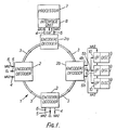
- this data transmission system may be used as a network for interconnecting communicating units such as one or more processors and one or more high-speed peripherals, for example disc storage units.
- the system has a central ring 1 consisting of encoder/ decoders 2 interconnected by transmission links 3 of coaxial cable.
- the encoder/decoders 2 act as interfaces of the ring 1 for communicating units that are connected to them.
- Data transmission takes place serially over each link 3 in the form of a modulated carrier. The transmission is in one direction only, as shown by the arrows.
- Each encoder/decoder 2 receives the data transmitted over its incoming link and demodulates it to recover the data in a non-return to zero (NRZ) format which it outputs to its attached communicating unit or units on a connection 4. It also recovers an accompanying clock signal which it outputs on a connection 5. It receives data in the same NRZ format from its attached communicating unit or units on a connection 6. It remodulates the carrier with this data to produce the signal output on its outgoing link 3.
- NRZ non-return to zero
- Each encoder/decoder 2 may act as the interface for a single one of the communicating units.
- the encoder/decoder 2a is shown connected to a single processor 7 through an interface unit 8.
- it may act as the interface for a number of such units through a subsidiary NRZ serial data loop.
- the encoder/decoder 2b is shown connected to disc storage units 9 through interface units 10 which are connected in a loop which starts as the connection 4b and returns as the connection 6b. Clock signals are distributed on lines 5b directly to each interface unit 10.
- the communicating units may use any suitable protocol for exchanging messages, such as those described in the above-mentioned paper by Clark et al.
- the data path may form a closed ring, with a control token passed from unit to unit as a go-ahead for transmission. (The data path diverts from the central ring 1 at each encoder/decoder 2 to loop through the unit or units for which it is the interface.)
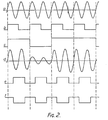
- Figure 2 shows various of the waveforms required to generate the modulated carrier transmitted over the links 3.
- Waveform a is the unmodulated carrier
- waveform b is the clock signal, the rising edges of which define the bit periods as shown by the dotted lines.
- An example of the data in NRZ format is shown as waveform c; the signal level remains substantially constant at one of two fixed levels for the whole of each bit period.
- the clock rate and the frequency of the carrier are related in such a way that each bit period contains a whole number of carrier cycles (two in this example).
- the carrier frequency is an integral multiple of the clock rate, which for NRZ data is the inverse of the bit period.
- the clock rate may be 50 MHZ (and consequently the data rate 50 million bits per second) and the carrier frequency 100 MHZ.
- the data signal is used to amplitude-modulate the carrier and the result is shown as waveform d.
- the level of modulation is chosen to give a significant difference between the amplitudes of the carrier when modulated by the two data levels, but nevertheless to give the carrier an appreciable amplitude even when modulated by the low data level.
- the modulated waveform passes over the links 3 with a relatively high immunity from electro-magnetically induced noise.
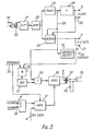
- each encoder/decoder 2 is coupled to a coaxial cable 3a forming its incoming transmission link by a transformer 20 connected to a high-pass filter 21, for example, a two-stage constant K passive high-pass network, which provides the necessary blocking of frequencies below 25 MHZ.
- the signal is then amplified by an amplifier 22 and passed to a tank circuit 23 which contains a tuned circuit of medium Q (a suitable value is 20) tuned to the frequency of the carrier. Its output, squared, is passed to a divider circuit 24 which outputs the clock signal both on a line 25 for use within the encoder/decoder and on the connection 5 for supply'to the associated communicating unit or units. It will be seen that the clock signal is very simply obtained. Because some amplitude of carrier is always present, the clock signal is always produced.
- the output of the amplifier 22 is also passed to a demodulator 26 (described in more detail below) which recovers the original NRZ data and outputs it as the received data on the connection 4 to the associated unit or units. It is also supplied on a line 27 for use within the encoder/decoder 2.
- the clock signal Since the clock signal is obtained by dividing the carrier by two, it has two possible phases, depending on which of the two carrier cycles within a bit period acts as the starting point. The phases differ by half a bit period and it is arbitrary which phase is adopted at the moment when generation of the clock signal starts.
- the clock signal is, however, timed so that the strobing point occurs (depending on the phase adopted) either one quarter or three-quarters way through the bit period, and the data signal level will therefore be sensed away from the points at which the data signal level can change, whichever phase the clock signal adopts.
- the carrier is also passed as a square waveform on a line 28 through an OR gate 29 to a modulator 30 (described in more detail below) where it is modulated by the outgoing data supplied from a multiplexer 31 in the same manner as described with reference to Figure 2, and is then output through a transformer 32 onto a co-axial cable 3b forming the outgoing transmission link for the encoder/decoder 2.
- a modulator 30 (described in more detail below) where it is modulated by the outgoing data supplied from a multiplexer 31 in the same manner as described with reference to Figure 2, and is then output through a transformer 32 onto a co-axial cable 3b forming the outgoing transmission link for the encoder/decoder 2.
- voltages as low as 100 mV may be used. Such voltages may conveniently be generated by LSI techniques.
- a communicating unit attached to the encoder/decoder 2 is operable it sends a control signal to that effect on a line 33 and also, on the line 6, its data to be transmitted.
- the "operable" signal causes the multiplexer 31 to select this data for supply to the modulator 30, from where it is output in modulated form to the central ring 1 on the cable 3b. If there is no such operable communicating unit there is no "operable" signal on the line 33 and the multiplexer 31 is caused to select the data on the line 4, that is the data received by the encoder/decoder 2, as the data to modulate the carrier.
- the encoder/ decoder acts as a simple repeater. The ring 1 is therefore not disabled even if none of the communicating units for which it acts as an interface to the ring are operative.
- a carrier-detect circuit 34 is provided. It responds to the absence of the expected variation in signal level on the line 28 to output a signal indicating the absence of carrier on a line 35.
- This line passes to the attached communicating unit(s).
- It is also combined in an AND gate 36 with the "operable" line 33 and the output of the gate 36 enables a local oscillator 37 tuned to the carrier frequency and connected to the modulator 30 through the OR-gate 29.
- the operable communicating unit may then send a message to a monitoring station elsewhere in the system informing it that there is a break in the ring and, to help locate the break, of its identity as the first operable unit downstream of the break.
- the demodulator 26 could be an integrator acting as an envelope detector in the conventional way, we prefer to use a digital demodulator, in view of the bandwidth required to recover the NRZ pulses.
- the demodulator 26 has two level detectors 40 and 41, one of which outputs a pulse whenever the modulated carrier exceeds a threshold in the positive direction and the other a pulse whenever it exceeds a threshold in the negative direction. The thresholds are selected so that only the greater of the two modulated amplitudes is sufficient to produce these pulses.
- the outputs of the level detectors 40 and 41 are ORed by a gate 42 and used to set a D-type bistable 43 clocked by the recovered carrier.
- the output of the bistable 43 is in turn used to set another D-type bistable clocked by the data clock at, as has been explained, either the one-quarter orthree-quarters point.
- the resultant output is the demodulated received data.
- the modulator consists of four transistors 44-47 driving the transformer 32 in push-pull.
- Two transistors 44 and 45 operate at a low collector current, and continuously transmit a residual carrier level.
- the other two transistors 46 and 47 operate at high collector current and only drive current through the output transformer in the presence of a logic 1.
- the secondary of the output transformer is shunted by a resistor 48 at the characteristic impedance of the line. This effectively series terminates the line; a necessity since the presence of the high pass filter at the far end of the line presents a high reactive impedance at low frequencies. Any reflections will be absorbed in the shunt. Its presence halves the available transmit amplitude; however the use of pushpull drive ensures more than adequate transmitter power.
- Isolation of the coaxial cable from the transmitter Ov by use of a transformer is not essential; however, it enables the outer of the coaxial cable to be resistively terminated at the transmitter. Any noise induced on the cable outer sheath can thereby be absorbed thus improving the noise immunity.
- each encoder/ decoder 2 detects carrier and its local oscillator 37 is not enabled. Hence there is a closed path for the carrier around the ring, passing along each link 2 and then, in each encoder/decoder 2, via the transformer 20, filter 21, amplifier 22, tank 23, modulator 30 and finally transformer 32 onto the next link 2. There is no external source simultaneously injecting a wave of the carrier frequency into this ring. But we have found that the carrier will nevertheless sustain itself because the whole ring acts as an oscillatory system. The approximate frequency is determined by the frequency to which the tanks 23 are tuned, but the exact frequency is determined by the ring as a whole and is such as to give an integral number of carrier cycles around the closed path of the carrier. In other words the carrier, after a complete circuit of the closed path, is in phase with itself.
- the length of the closed path for the carrier is liable to vary, principally because the lengths of the cables 3 vary with temperature and age. If the carrier frequency were constant that would change the phase relationship after a complete circuit and impair or prevent the sustaining of the carrier waveform. However, we have found that the carrier frequency adjusts itself automatically to maintain an integral number of carrier cycles round the closed path. The data-clock rate will change correspondingly (over a small range) and is therefore also determined by the properties of the ring itself rather than any external equipment.
- the carrier self-sustaining, but it is also capable of establishing itself spontaneously when the ring is first brought into operation, because of the oscillatory nature of the ring.
- this property could be used in the system described, in fact it is not used, because the presence of the local oscillators provided as a safeguard against the ring's breaking.
- the ring When the ring is first switched on they will all be enabled by the absence of any incoming carrier and each will inject its own carrier into the ring. But as each encoder/decoder detects incoming carrier its oscillator will be disabled, and finally the carrier will be left in its selfsustaining mode with no independent external source. At this point the communicating units using the ring can start to pass messages.
- Figure 1 shows the carrier and modulated waveform in idealised form a sinusoids
- the modulator 30 in fact receives the carrier as a square waveform and outputs it in modulated form likewise as a square waveform, each pair of cycles having one of two amplitudes depending on the value of the modulating data.
- the various following components including in particular the transmission cable, are bandwidth- limited and serve to round the waveform towards that shown in waveform d of Figure 1. This rounding is no disadvantage since the demodulating method does not need to sense edges but rather amplitude of the carrier.
- Attenuation may be 30 dB at 25 MHz, with the 3 dB point at 50 MHz.
- the lowest frequency that must be substantially completely passed is the carrier frequency less half the bit rate - 75 MHz for the example given.
- the two rates and the filter are selected with this criterion and the need to allow substantially complete attenuation at 25 MHz in mind.
- the divider 24 may in fact be a chain of divide-by-two circuits, a particular output of which is selected by a multiplexer to give a desired data rate. Smaller data rates for a given carrier require small bandwidths and allow a longer link between units. One bit per cycle is possible but has a rather wide bandwidth, leading to rather short maximum permissible links.
- the carrier is at least 50 MHz, frequencies below 25 MHz being filtered out. But if good noise immunity is not required, lower frequencies may be used and the filter omitted.
- the encoders/decoders may output clock and NRZ data in a two-phase form.
- the clock signal is split into two half-rate signals in antiphase with one another and the data is split into two signals one the result of strobing the data with one of these clock signals and the other the result of strobing it with the other of these clock signals.
- the two phases of data are combined by strobing each with its own phase of clock signal. This arrangement increases the latitude for timing uncertainties such as are especially likely to occur if a fast form of logic such as ECL is used in the encoder/ decoder and conversion takes place to levels suitable for a slower form of logic such as TTL which is used in the interface units 10. Data may then similarly be returned from the interface in two-phase form.
- An alternative method of combining the data with the carrier for transmission over the links 3 also uses a carrier with two cycles per bit.
- the format is bipolar: starting from a carrier oscillating between 0 and a positive level, to represent one binary value one of the positive-going excursions is inverted; to represent the other the other positive-going excursion is inverted.
- the carrier is then recovered by rectification.
Landscapes
- Engineering & Computer Science (AREA)
- Computer Networks & Wireless Communication (AREA)
- Signal Processing (AREA)
- Power Engineering (AREA)
- Synchronisation In Digital Transmission Systems (AREA)
- Dc Digital Transmission (AREA)
Description
- This invention relates to data transmission systems, especially of the kind that can function as a local area network. In a local area network a number of devices - often computer processors or peripherals - are connected together by transmission links to allow them to communicate with one another, the devices being sufficiently close together to allow the transmission links to be relatively simple and reliable. A survey of such networks is to be found in "An introduction to local area networks" by D. D. Clark, K. T. Pogran, and D. P. Reed in the Proceedings of IEEE, November 1978, pages 1497 to 1516, which describes various possible topographies for interconnecting the units. In one of these topographies the devices are connected in a ring by unidirectional links so that data from any one device can pass through all the others until it reaches its destination. Each device is commonly connected to the ring through an interface unit that recovers both data and clock from an incoming transmission link and, using the recovered clock, either repeats the data onto an outgoing link or substitutes data from the associated device.
- Closing such a transmission system on itself to form a ring for the passage of data causes grave problems. If the network is considered as a sequential string of links and interface units that is closed back upon itself at a certain point then there is an arbitrary phase difference at that point between the incoming and outgoing signals. This difference varies with time because the length of the ring can change with temperature and ageing. The normal approach of which US Patent No. 3,597,549 is an example, is therefore to include somt kind of ring closure element. This element includes a master source for clock signals, which then propagate around the ring, being recovered at each interface unit until they return to the ring closure element. At the ring closure element the arbitrary phase difference between the incoming data and the master is accommodated by an elastic buffer, a first-in first-out buffer (FIFO) into which data is clocked by the received clock and from which it is clocked by the master source. The closure element therefore acts as a bridge for data but provides a break in the clock transmission that decouples the outgoing clock from the incoming clock.
- In the above mentioned US patent specification data is represented by a bipolar format which for this specification is to be regarded as the combination of the data with a carrier of twice the data rate. This carrier is recovered in each interface unit as a prelude to recovering the clock signal, which is then used to recover the data. Provided the interface unit is not also the closure element the carrier is recombined with data for transmission to the next interface unit.
- The object of this invention is to accommodate variations in the length of the ring without the use of a ring closure element.
- According to the invention, there is provided a data transmission system comprising a plurality of encoder/decoders connected in a ring by transmission links over which in operation data passes in a predetermined direction as a signal combining the data and a carrier, each encoder/decoder comprising means for recovering the carrier from the signal received at its incoming transmission link, means for recovering a data signal from the signal received at its incoming transmission link and means connected to receive the recovered carrier for recombining it with a data signal from output over the encoder/decoder's outgoing transmission link, characterised in that the connection in every encoder/decoder from its incoming transmission link to its outgoing transmission link via its means for recovering the carrier and its means for recombining the carrier with a data signal, together with the intervening transmission links, form, a closed path around which in operation a waveform containing the carrier circulates, the waveform once initiated being sustained by the ring as a whole acting as an oscillatory system without any introduction of the waveform from an independent source and the frequency of the carrier being constant around the ring and adjusting itself in accordance with variations in the length of the ring in such a manner as to maintain an integral number of carrier cycles around the said closed path.
- Therefore, instead of having a path for the carrier that has both a beginning at a master source and an end, there is a closed path. The applicants find that this path sustains an oscillation which may be used as a carrier. Variations in the length of the ring are accommodated by changes in the frequency of the carrier rather than by an elastic buffer.
- European Patent Application No. A-0 011 015 and French Patent Application No. A-2 305 074 disclose repeaters which recover a carrier and a data signal and remodulate the carrier with the data signal. However, these systems are point-to- point systems in which one end station sends data to another, and the object of the repeaters is simply to extend the distance over which one end station can communicate with another. The IBM Technical Disclosure Bulletin, Vol. 18, No. 10 March 1876, pages 3368 and 3369, disclose a frequency-division multiplexing system in which a number of stations communicate over a broadband cable and all derive their receive and transmit clocks from a common external reference source.
- An example of a system in accordance with the invention will now be described in greater detail with reference to the accompanying drawings, in which:
- Figure 1 is a diagram of the overall system;
- Figure 2 shows in idealised form various waveforms used in the system;
- Figure 3 is a block diagram of the encoder/ decoder of the system;
- Figure 4 is a block diagram of the demodulator of the encoder/decoder; and
- Figure 5 is a block diagram of the modulator of the encoder/decoder.
- Referring to Figure 1, this data transmission system may be used as a network for interconnecting communicating units such as one or more processors and one or more high-speed peripherals, for example disc storage units. The system has a
central ring 1 consisting of encoder/decoders 2 interconnected bytransmission links 3 of coaxial cable. The encoder/decoders 2 act as interfaces of thering 1 for communicating units that are connected to them. Data transmission takes place serially over eachlink 3 in the form of a modulated carrier. The transmission is in one direction only, as shown by the arrows. - Each encoder/
decoder 2 receives the data transmitted over its incoming link and demodulates it to recover the data in a non-return to zero (NRZ) format which it outputs to its attached communicating unit or units on aconnection 4. It also recovers an accompanying clock signal which it outputs on aconnection 5. It receives data in the same NRZ format from its attached communicating unit or units on aconnection 6. It remodulates the carrier with this data to produce the signal output on itsoutgoing link 3. - Each encoder/
decoder 2 may act as the interface for a single one of the communicating units. As an illustration the encoder/decoder 2a is shown connected to asingle processor 7 through aninterface unit 8. Alternatively, it may act as the interface for a number of such units through a subsidiary NRZ serial data loop. As an illustration, the encoder/decoder 2b is shown connected to disc storage units 9 throughinterface units 10 which are connected in a loop which starts as theconnection 4b and returns as theconnection 6b. Clock signals are distributed onlines 5b directly to eachinterface unit 10. - The communicating units may use any suitable protocol for exchanging messages, such as those described in the above-mentioned paper by Clark et al. As an example, the data path may form a closed ring, with a control token passed from unit to unit as a go-ahead for transmission. (The data path diverts from the
central ring 1 at each encoder/decoder 2 to loop through the unit or units for which it is the interface.) - Figure 2 shows various of the waveforms required to generate the modulated carrier transmitted over the
links 3. Waveform a is the unmodulated carrier, and waveform b is the clock signal, the rising edges of which define the bit periods as shown by the dotted lines. An example of the data in NRZ format is shown as waveform c; the signal level remains substantially constant at one of two fixed levels for the whole of each bit period. - The clock rate and the frequency of the carrier are related in such a way that each bit period contains a whole number of carrier cycles (two in this example). In other words the carrier frequency is an integral multiple of the clock rate, which for NRZ data is the inverse of the bit period.
- As an example of suitable values, the clock rate may be 50 MHZ (and consequently the data rate 50 million bits per second) and the carrier frequency 100 MHZ.
- The data signal is used to amplitude-modulate the carrier and the result is shown as waveform d. The level of modulation is chosen to give a significant difference between the amplitudes of the carrier when modulated by the two data levels, but nevertheless to give the carrier an appreciable amplitude even when modulated by the low data level.
- We have found that, provided frequencies below 25 NHZ are filtered out, the modulated waveform passes over the
links 3 with a relatively high immunity from electro-magnetically induced noise. - Referring to Figure 3, each encoder/
decoder 2 is coupled to acoaxial cable 3a forming its incoming transmission link by atransformer 20 connected to a high-pass filter 21, for example, a two-stage constant K passive high-pass network, which provides the necessary blocking of frequencies below 25 MHZ. The signal is then amplified by anamplifier 22 and passed to atank circuit 23 which contains a tuned circuit of medium Q (a suitable value is 20) tuned to the frequency of the carrier. Its output, squared, is passed to adivider circuit 24 which outputs the clock signal both on aline 25 for use within the encoder/decoder and on theconnection 5 for supply'to the associated communicating unit or units. It will be seen that the clock signal is very simply obtained. Because some amplitude of carrier is always present, the clock signal is always produced. - The output of the
amplifier 22 is also passed to a demodulator 26 (described in more detail below) which recovers the original NRZ data and outputs it as the received data on theconnection 4 to the associated unit or units. It is also supplied on aline 27 for use within the encoder/decoder 2. - Since the clock signal is obtained by dividing the carrier by two, it has two possible phases, depending on which of the two carrier cycles within a bit period acts as the starting point. The phases differ by half a bit period and it is arbitrary which phase is adopted at the moment when generation of the clock signal starts. The clock signal is, however, timed so that the strobing point occurs (depending on the phase adopted) either one quarter or three-quarters way through the bit period, and the data signal level will therefore be sensed away from the points at which the data signal level can change, whichever phase the clock signal adopts.
- Taking waveform c of Figure 2 to show the demodulated data signal, and assuming the rising edge of the clock signal is used for strobing, the two possible states of the clock signal are shown in Figure 2 as waveforms e and f.
- The carrier is also passed as a square waveform on a
line 28 through anOR gate 29 to a modulator 30 (described in more detail below) where it is modulated by the outgoing data supplied from amultiplexer 31 in the same manner as described with reference to Figure 2, and is then output through atransformer 32 onto aco-axial cable 3b forming the outgoing transmission link for the encoder/decoder 2. Because of the noise immunity of the system, voltages as low as 100 mV may be used. Such voltages may conveniently be generated by LSI techniques. - Provided a communicating unit attached to the encoder/
decoder 2 is operable it sends a control signal to that effect on a line 33 and also, on theline 6, its data to be transmitted. The "operable" signal causes themultiplexer 31 to select this data for supply to themodulator 30, from where it is output in modulated form to thecentral ring 1 on thecable 3b. If there is no such operable communicating unit there is no "operable" signal on the line 33 and themultiplexer 31 is caused to select the data on theline 4, that is the data received by the encoder/decoder 2, as the data to modulate the carrier. In this case, the encoder/ decoder acts as a simple repeater. Thering 1 is therefore not disabled even if none of the communicating units for which it acts as an interface to the ring are operative. - To cope with a break in the
ring 1 and the resultant loss of carrier, a carrier-detectcircuit 34 is provided. It responds to the absence of the expected variation in signal level on theline 28 to output a signal indicating the absence of carrier on aline 35. This line passes to the attached communicating unit(s). It is also combined in an ANDgate 36 with the "operable" line 33 and the output of thegate 36 enables alocal oscillator 37 tuned to the carrier frequency and connected to themodulator 30 through the OR-gate 29. Hence if no carrier is detected on thering 1 and an associated communicating unit is operable, locally generated carrier will be supplied instead and used by subsequent encoder/decoders. The operable communicating unit may then send a message to a monitoring station elsewhere in the system informing it that there is a break in the ring and, to help locate the break, of its identity as the first operable unit downstream of the break. - Although the
demodulator 26 could be an integrator acting as an envelope detector in the conventional way, we prefer to use a digital demodulator, in view of the bandwidth required to recover the NRZ pulses. Referring to Figure 4, thedemodulator 26 has twolevel detectors level detectors gate 42 and used to set a D-type bistable 43 clocked by the recovered carrier. The output of the bistable 43 is in turn used to set another D-type bistable clocked by the data clock at, as has been explained, either the one-quarter orthree-quarters point. The resultant output is the demodulated received data. - Referring to Figure 5 the modulator consists of four transistors 44-47 driving the
transformer 32 in push-pull. Twotransistors transistors logic 1. The secondary of the output transformer is shunted by aresistor 48 at the characteristic impedance of the line. This effectively series terminates the line; a necessity since the presence of the high pass filter at the far end of the line presents a high reactive impedance at low frequencies. Any reflections will be absorbed in the shunt. Its presence halves the available transmit amplitude; however the use of pushpull drive ensures more than adequate transmitter power. Isolation of the coaxial cable from the transmitter Ov by use of a transformer is not essential; however, it enables the outer of the coaxial cable to be resistively terminated at the transmitter. Any noise induced on the cable outer sheath can thereby be absorbed thus improving the noise immunity. - In normal operation of the ring each encoder/
decoder 2 detects carrier and itslocal oscillator 37 is not enabled. Hence there is a closed path for the carrier around the ring, passing along eachlink 2 and then, in each encoder/decoder 2, via thetransformer 20,filter 21,amplifier 22,tank 23,modulator 30 and finallytransformer 32 onto thenext link 2. There is no external source simultaneously injecting a wave of the carrier frequency into this ring. But we have found that the carrier will nevertheless sustain itself because the whole ring acts as an oscillatory system. The approximate frequency is determined by the frequency to which thetanks 23 are tuned, but the exact frequency is determined by the ring as a whole and is such as to give an integral number of carrier cycles around the closed path of the carrier. In other words the carrier, after a complete circuit of the closed path, is in phase with itself. - The length of the closed path for the carrier is liable to vary, principally because the lengths of the
cables 3 vary with temperature and age. If the carrier frequency were constant that would change the phase relationship after a complete circuit and impair or prevent the sustaining of the carrier waveform. However, we have found that the carrier frequency adjusts itself automatically to maintain an integral number of carrier cycles round the closed path. The data-clock rate will change correspondingly (over a small range) and is therefore also determined by the properties of the ring itself rather than any external equipment. - Not only is the carrier self-sustaining, but it is also capable of establishing itself spontaneously when the ring is first brought into operation, because of the oscillatory nature of the ring. However, although this property could be used in the system described, in fact it is not used, because the presence of the local oscillators provided as a safeguard against the ring's breaking. When the ring is first switched on they will all be enabled by the absence of any incoming carrier and each will inject its own carrier into the ring. But as each encoder/decoder detects incoming carrier its oscillator will be disabled, and finally the carrier will be left in its selfsustaining mode with no independent external source. At this point the communicating units using the ring can start to pass messages.
- Considerable problems have been experienced in previous attempts to close a communications ring. For example, if phase-locked oscillators are used to derive the required clock signals, the clock jitter occurring at each oscillator is compounded from stage to stage and causes stability problems that can limit the number of stages possible. We find that deriving the clock signal from the modulated carrier avoids this problem and leads to a stable system in which the number of stages is not limited in this way.
- And if the data path itself is closed so that data can loop through all the encoder/decoders, for example to allow messages to make a complete circuit of the data path, the additional requirement exists that data which has made a complete circulation of the data path must still be in phase with itself. This has been expressed as the requirement that there should be an integral number of bits on the closed data path, and it has been proposed to insert a special device acting in effect as an elastic buffer to provide the required synchronism.
- We find that the system described allows complete circulation of bits with no such device. The reason is as follows. Data that has made a complete circulation can in any case be in only one of two phase relationships with its earlier passage, that is in phase or 180° out of phase, since there must be an integral number of carrier cycles round the closed path and there are two carrier cycles per bit. However, even though data can enter an encoder/decoder in either of two states differing in phase by half a bit, this difference is accommodated within the encoder/decoder by the clocking method described which strobes the data away from an edge, and the resultant data signal is in phase with its previous passage.
- Although Figure 1 shows the carrier and modulated waveform in idealised form a sinusoids, the
modulator 30 in fact receives the carrier as a square waveform and outputs it in modulated form likewise as a square waveform, each pair of cycles having one of two amplitudes depending on the value of the modulating data. However, the various following components, including in particular the transmission cable, are bandwidth- limited and serve to round the waveform towards that shown in waveform d of Figure 1. This rounding is no disadvantage since the demodulating method does not need to sense edges but rather amplitude of the carrier. - Therefore the limits on the acceptable lengths of cable used do not depend on the extent the shape is changed, but only on the overall drop in level. If that falls to an unacceptably small level analogue amplification may be used to restore it: not digital regeneration is required.
- As has been mentioned, for good noise immunity substantially all the frequencies below 25 MHz should be filtered out at the entrance to each encoder/decoder. As an example, with a carrier frequency of 100 MHz and a bit rate of 50 MHz and using a filter as described, attenuation may be 30 dB at 25 MHz, with the 3 dB point at 50 MHz. The lowest frequency that must be substantially completely passed is the carrier frequency less half the bit rate - 75 MHz for the example given. For good noise immunity the two rates and the filter are selected with this criterion and the need to allow substantially complete attenuation at 25 MHz in mind.
- Various modifications may be made to the system described.
- There may be other than two carrier cycles per bit. Assuming that the carrier frequency is kept constant, the
divider 24 may in fact be a chain of divide-by-two circuits, a particular output of which is selected by a multiplexer to give a desired data rate. Smaller data rates for a given carrier require small bandwidths and allow a longer link between units. One bit per cycle is possible but has a rather wide bandwidth, leading to rather short maximum permissible links. Preferably the carrier is at least 50 MHz, frequencies below 25 MHz being filtered out. But if good noise immunity is not required, lower frequencies may be used and the filter omitted. - For high date rates the encoders/decoders may output clock and NRZ data in a two-phase form. The clock signal is split into two half-rate signals in antiphase with one another and the data is split into two signals one the result of strobing the data with one of these clock signals and the other the result of strobing it with the other of these clock signals. In the
interface units interface units 10. Data may then similarly be returned from the interface in two-phase form. - An alternative method of combining the data with the carrier for transmission over the
links 3 also uses a carrier with two cycles per bit. The format is bipolar: starting from a carrier oscillating between 0 and a positive level, to represent one binary value one of the positive-going excursions is inverted; to represent the other the other positive-going excursion is inverted. The carrier is then recovered by rectification.
Claims (10)
Applications Claiming Priority (2)
| Application Number | Priority Date | Filing Date | Title |
|---|---|---|---|
| GB8105133 | 1981-02-18 | ||
| GB8105133 | 1981-02-18 |
Publications (2)
| Publication Number | Publication Date |
|---|---|
| EP0058573A1 EP0058573A1 (en) | 1982-08-25 |
| EP0058573B1 true EP0058573B1 (en) | 1985-06-19 |
Family
ID=10519796
Family Applications (1)
| Application Number | Title | Priority Date | Filing Date |
|---|---|---|---|
| EP82300812A Expired EP0058573B1 (en) | 1981-02-18 | 1982-02-17 | Data transmission system with transmission links joined in a ring |
Country Status (5)
| Country | Link |
|---|---|
| US (1) | US4435705A (en) |
| EP (1) | EP0058573B1 (en) |
| AU (1) | AU547571B2 (en) |
| DE (1) | DE3264173D1 (en) |
| ZA (1) | ZA82860B (en) |
Families Citing this family (8)
| Publication number | Priority date | Publication date | Assignee | Title |
|---|---|---|---|---|
| FR2526249A1 (en) * | 1982-04-30 | 1983-11-04 | Labo Electronique Physique | METHOD AND DEVICE FOR AUTOMATICALLY TIMING STATIONS IN A TIME MULTIPLEX FOR OPTICAL BUS AND DATA TRANSMISSION AND PROCESSING SYSTEM COMPRISING SUCH A DEVICE |
| US4527270A (en) * | 1983-05-04 | 1985-07-02 | Allen-Bradley Company | Communications network with stations that detect and automatically bypass faults |
| US4587651A (en) * | 1983-05-04 | 1986-05-06 | Cxc Corporation | Distributed variable bandwidth switch for voice, data, and image communications |
| US4628307A (en) * | 1984-12-18 | 1986-12-09 | International Business Machines Corp. | FET switch for high frequency signals |
| IT1182404B (en) * | 1985-02-04 | 1987-10-05 | Fiat Ricerche | SYSTEM FOR THE CONNECTION OF SENSOR DEVICES TO ACTUATOR DEVICES |
| DE3688073T2 (en) * | 1986-04-03 | 1993-06-24 | Otis Elevator Co | TWO-WAY RING CONNECTION SYSTEM FOR ELEVATOR GROUP CONTROL. |
| US5815295A (en) * | 1993-03-11 | 1998-09-29 | Lucent Technologies Inc. | Optical communication system with improved maintenance capabilities |
| CA2118616C (en) * | 1993-03-11 | 1999-09-14 | Thomas Edward Darcie | Optical network based on remote interrogation of terminal equipment |
Citations (1)
| Publication number | Priority date | Publication date | Assignee | Title |
|---|---|---|---|---|
| US3597549A (en) * | 1969-07-17 | 1971-08-03 | Bell Telephone Labor Inc | High speed data communication system |
Family Cites Families (12)
| Publication number | Priority date | Publication date | Assignee | Title |
|---|---|---|---|---|
| US3582782A (en) | 1968-04-24 | 1971-06-01 | Bell Telephone Labor Inc | Harmonic sine wave data transmission system |
| US3744051A (en) | 1971-08-31 | 1973-07-03 | Computer Transmission Corp | Computer interface coding and decoding apparatus |
| JPS5010906A (en) * | 1973-05-28 | 1975-02-04 | ||
| LU74290A1 (en) * | 1975-03-20 | 1976-06-18 | ||
| GB1530405A (en) | 1975-03-24 | 1978-11-01 | Okura Denki Co Ltd | Loop data highway communication system |
| US4042783A (en) | 1976-08-11 | 1977-08-16 | International Business Machines Corporation | Method and apparatus for byte and frame synchronization on a loop system coupling a CPU channel to bulk storage devices |
| US4121050A (en) | 1977-02-02 | 1978-10-17 | The United States Of America As Represented By The Secretary Of The Air Force | Differential tri-phase shift keyed modulation |
| US4086534A (en) | 1977-02-14 | 1978-04-25 | Network Systems Corporation | Circuit for wire transmission of high frequency data communication pulse signals |
| US4199662A (en) | 1978-07-17 | 1980-04-22 | Lowe Charles S Jr | Hybrid control of time division multiplexing |
| FR2440660A1 (en) * | 1978-10-31 | 1980-05-30 | Thomson Csf | DIGITAL HERTZIAN REPEATER WITH REGENERATION AND TRANSMISSION NETWORK COMPRISING SUCH REPEATERS |
| US4284843A (en) * | 1979-05-10 | 1981-08-18 | General Electric Company | Repeating station for use in digital data communications link |
| US4304001A (en) | 1980-01-24 | 1981-12-01 | Forney Engineering Company | Industrial control system with interconnected remotely located computer control units |
-
1982
- 1982-02-10 ZA ZA82860A patent/ZA82860B/en unknown
- 1982-02-16 US US06/348,942 patent/US4435705A/en not_active Expired - Fee Related
- 1982-02-17 AU AU80548/82A patent/AU547571B2/en not_active Ceased
- 1982-02-17 DE DE8282300812T patent/DE3264173D1/en not_active Expired
- 1982-02-17 EP EP82300812A patent/EP0058573B1/en not_active Expired
Patent Citations (2)
| Publication number | Priority date | Publication date | Assignee | Title |
|---|---|---|---|---|
| US3597549A (en) * | 1969-07-17 | 1971-08-03 | Bell Telephone Labor Inc | High speed data communication system |
| US3597549B1 (en) * | 1969-07-17 | 1983-12-06 |
Also Published As
| Publication number | Publication date |
|---|---|
| EP0058573A1 (en) | 1982-08-25 |
| ZA82860B (en) | 1982-12-29 |
| DE3264173D1 (en) | 1985-07-25 |
| US4435705A (en) | 1984-03-06 |
| AU8054882A (en) | 1982-08-26 |
| AU547571B2 (en) | 1985-10-24 |
Similar Documents
| Publication | Publication Date | Title |
|---|---|---|
| JPH055710Y2 (en) | ||
| EP1112648B1 (en) | A system and method for sending and receiving data signals over a clock signal line | |
| US5090025A (en) | Token ring synchronization | |
| US4592072A (en) | Decoder for self-clocking serial data communications | |
| US5276712A (en) | Method and apparatus for clock recovery in digital communication systems | |
| US4528661A (en) | Ring communications system | |
| EP1648128B1 (en) | Selective scrambler for use in a communication system and method to minimize bit error at the receiver | |
| US4972161A (en) | Clock recovery for serial data communications system | |
| JPH042023B2 (en) | ||
| US4435705A (en) | Data transmission systems | |
| US4604756A (en) | Device for recovering a synchronized clock signal from a signal sequence | |
| US5602873A (en) | Flash NRZI infrared modem | |
| US4438520A (en) | System for regenerating a data word on a communications ring | |
| US5418496A (en) | Serial data clock recovery circuit using dual oscillator circuit | |
| US5535337A (en) | Port circuit for a token ring concentrator having phase lock loop timing recovery with additional circuitry to verify appropriate signals | |
| US3335369A (en) | System for data communication by phase shift of square wave carrier | |
| EP1334594A2 (en) | Apparatus and method for sending and receiving data signals over a clock signal line by pulse width modulation | |
| US4782484A (en) | Encoding and decoding signals for transmission over a multi-access medium | |
| US5524109A (en) | Token ring concentrator having retiming function | |
| JPS62102648A (en) | Acquisition pull-in circuit for carrier wave recovery from QAM signal | |
| JP2572984B2 (en) | Phase coherent demodulator | |
| US5309475A (en) | Data interchange network | |
| AU588479B2 (en) | A capture circuit for restoring the carrier from a qam-signal | |
| JPS601928A (en) | Modem/demodulator reception control method | |
| JPH04179346A (en) | Data repeater system |
Legal Events
| Date | Code | Title | Description |
|---|---|---|---|
| PUAI | Public reference made under article 153(3) epc to a published international application that has entered the european phase |
Free format text: ORIGINAL CODE: 0009012 |
|
| AK | Designated contracting states |
Designated state(s): BE DE FR GB NL SE |
|
| 17P | Request for examination filed |
Effective date: 19820917 |
|
| GRAA | (expected) grant |
Free format text: ORIGINAL CODE: 0009210 |
|
| AK | Designated contracting states |
Designated state(s): BE DE FR GB NL SE |
|
| REF | Corresponds to: |
Ref document number: 3264173 Country of ref document: DE Date of ref document: 19850725 |
|
| ET | Fr: translation filed | ||
| PLBE | No opposition filed within time limit |
Free format text: ORIGINAL CODE: 0009261 |
|
| STAA | Information on the status of an ep patent application or granted ep patent |
Free format text: STATUS: NO OPPOSITION FILED WITHIN TIME LIMIT |
|
| 26N | No opposition filed | ||
| PGFP | Annual fee paid to national office [announced via postgrant information from national office to epo] |
Ref country code: GB Payment date: 19910109 Year of fee payment: 10 |
|
| PGFP | Annual fee paid to national office [announced via postgrant information from national office to epo] |
Ref country code: SE Payment date: 19910218 Year of fee payment: 10 |
|
| PGFP | Annual fee paid to national office [announced via postgrant information from national office to epo] |
Ref country code: NL Payment date: 19910228 Year of fee payment: 10 |
|
| PGFP | Annual fee paid to national office [announced via postgrant information from national office to epo] |
Ref country code: BE Payment date: 19910311 Year of fee payment: 10 |
|
| PGFP | Annual fee paid to national office [announced via postgrant information from national office to epo] |
Ref country code: DE Payment date: 19910420 Year of fee payment: 10 |
|
| PGFP | Annual fee paid to national office [announced via postgrant information from national office to epo] |
Ref country code: FR Payment date: 19911230 Year of fee payment: 11 |
|
| PG25 | Lapsed in a contracting state [announced via postgrant information from national office to epo] |
Ref country code: GB Effective date: 19920217 |
|
| PG25 | Lapsed in a contracting state [announced via postgrant information from national office to epo] |
Ref country code: SE Effective date: 19920218 |
|
| PG25 | Lapsed in a contracting state [announced via postgrant information from national office to epo] |
Ref country code: BE Effective date: 19920228 |
|
| BERE | Be: lapsed |
Owner name: INTERNATIONAL COMPUTERS LTD Effective date: 19920228 |
|
| PG25 | Lapsed in a contracting state [announced via postgrant information from national office to epo] |
Ref country code: NL Effective date: 19920901 |
|
| GBPC | Gb: european patent ceased through non-payment of renewal fee | ||
| NLV4 | Nl: lapsed or anulled due to non-payment of the annual fee | ||
| PG25 | Lapsed in a contracting state [announced via postgrant information from national office to epo] |
Ref country code: DE Effective date: 19921103 |
|
| PG25 | Lapsed in a contracting state [announced via postgrant information from national office to epo] |
Ref country code: FR Effective date: 19931029 |
|
| REG | Reference to a national code |
Ref country code: FR Ref legal event code: ST |
|
| EUG | Se: european patent has lapsed |
Ref document number: 82300812.3 Effective date: 19920904 |