EP0051532B1 - Regulated mos substrate bias voltage generator for a static random access memory - Google Patents
Regulated mos substrate bias voltage generator for a static random access memory Download PDFInfo
- Publication number
- EP0051532B1 EP0051532B1 EP81401719A EP81401719A EP0051532B1 EP 0051532 B1 EP0051532 B1 EP 0051532B1 EP 81401719 A EP81401719 A EP 81401719A EP 81401719 A EP81401719 A EP 81401719A EP 0051532 B1 EP0051532 B1 EP 0051532B1
- Authority
- EP
- European Patent Office
- Prior art keywords
- current
- oscillator
- memory
- bias voltage
- output
- Prior art date
- Legal status (The legal status is an assumption and is not a legal conclusion. Google has not performed a legal analysis and makes no representation as to the accuracy of the status listed.)
- Expired
Links
- 239000000758 substrate Substances 0.000 title claims description 26
- 230000001105 regulatory effect Effects 0.000 title claims description 10
- 230000003068 static effect Effects 0.000 title claims description 9
- 230000002401 inhibitory effect Effects 0.000 claims description 10
- 230000001276 controlling effect Effects 0.000 claims description 5
- 230000004044 response Effects 0.000 claims 1
- 239000004020 conductor Substances 0.000 description 31
- 230000033228 biological regulation Effects 0.000 description 5
- 238000010276 construction Methods 0.000 description 2
- 239000007787 solid Substances 0.000 description 2
- XUIMIQQOPSSXEZ-UHFFFAOYSA-N Silicon Chemical compound [Si] XUIMIQQOPSSXEZ-UHFFFAOYSA-N 0.000 description 1
- 239000003990 capacitor Substances 0.000 description 1
- 230000007423 decrease Effects 0.000 description 1
- 238000010586 diagram Methods 0.000 description 1
- 238000013021 overheating Methods 0.000 description 1
- 238000005086 pumping Methods 0.000 description 1
- 238000005070 sampling Methods 0.000 description 1
- 229910052710 silicon Inorganic materials 0.000 description 1
- 239000010703 silicon Substances 0.000 description 1
Images
Classifications
-
- G—PHYSICS
- G05—CONTROLLING; REGULATING
- G05F—SYSTEMS FOR REGULATING ELECTRIC OR MAGNETIC VARIABLES
- G05F3/00—Non-retroactive systems for regulating electric variables by using an uncontrolled element, or an uncontrolled combination of elements, such element or such combination having self-regulating properties
- G05F3/02—Regulating voltage or current
- G05F3/08—Regulating voltage or current wherein the variable is DC
- G05F3/10—Regulating voltage or current wherein the variable is DC using uncontrolled devices with non-linear characteristics
- G05F3/16—Regulating voltage or current wherein the variable is DC using uncontrolled devices with non-linear characteristics being semiconductor devices
- G05F3/20—Regulating voltage or current wherein the variable is DC using uncontrolled devices with non-linear characteristics being semiconductor devices using diode- transistor combinations
- G05F3/205—Substrate bias-voltage generators
-
- G—PHYSICS
- G11—INFORMATION STORAGE
- G11C—STATIC STORES
- G11C11/00—Digital stores characterised by the use of particular electric or magnetic storage elements; Storage elements therefor
- G11C11/21—Digital stores characterised by the use of particular electric or magnetic storage elements; Storage elements therefor using electric elements
- G11C11/34—Digital stores characterised by the use of particular electric or magnetic storage elements; Storage elements therefor using electric elements using semiconductor devices
- G11C11/40—Digital stores characterised by the use of particular electric or magnetic storage elements; Storage elements therefor using electric elements using semiconductor devices using transistors
- G11C11/41—Digital stores characterised by the use of particular electric or magnetic storage elements; Storage elements therefor using electric elements using semiconductor devices using transistors forming static cells with positive feedback, i.e. cells not needing refreshing or charge regeneration, e.g. bistable multivibrator or Schmitt trigger
- G11C11/413—Auxiliary circuits, e.g. for addressing, decoding, driving, writing, sensing, timing or power reduction
-
- G—PHYSICS
- G11—INFORMATION STORAGE
- G11C—STATIC STORES
- G11C5/00—Details of stores covered by group G11C11/00
- G11C5/14—Power supply arrangements, e.g. power down, chip selection or deselection, layout of wirings or power grids, or multiple supply levels
- G11C5/145—Applications of charge pumps; Boosted voltage circuits; Clamp circuits therefor
- G11C5/146—Substrate bias generators
-
- H—ELECTRICITY
- H02—GENERATION; CONVERSION OR DISTRIBUTION OF ELECTRIC POWER
- H02M—APPARATUS FOR CONVERSION BETWEEN AC AND AC, BETWEEN AC AND DC, OR BETWEEN DC AND DC, AND FOR USE WITH MAINS OR SIMILAR POWER SUPPLY SYSTEMS; CONVERSION OF DC OR AC INPUT POWER INTO SURGE OUTPUT POWER; CONTROL OR REGULATION THEREOF
- H02M3/00—Conversion of DC power input into DC power output
- H02M3/02—Conversion of DC power input into DC power output without intermediate conversion into AC
- H02M3/04—Conversion of DC power input into DC power output without intermediate conversion into AC by static converters
- H02M3/06—Conversion of DC power input into DC power output without intermediate conversion into AC by static converters using resistors or capacitors, e.g. potential divider
- H02M3/07—Conversion of DC power input into DC power output without intermediate conversion into AC by static converters using resistors or capacitors, e.g. potential divider using capacitors charged and discharged alternately by semiconductor devices with control electrode, e.g. charge pumps
-
- H—ELECTRICITY
- H02—GENERATION; CONVERSION OR DISTRIBUTION OF ELECTRIC POWER
- H02M—APPARATUS FOR CONVERSION BETWEEN AC AND AC, BETWEEN AC AND DC, OR BETWEEN DC AND DC, AND FOR USE WITH MAINS OR SIMILAR POWER SUPPLY SYSTEMS; CONVERSION OF DC OR AC INPUT POWER INTO SURGE OUTPUT POWER; CONTROL OR REGULATION THEREOF
- H02M3/00—Conversion of DC power input into DC power output
- H02M3/02—Conversion of DC power input into DC power output without intermediate conversion into AC
- H02M3/04—Conversion of DC power input into DC power output without intermediate conversion into AC by static converters
- H02M3/06—Conversion of DC power input into DC power output without intermediate conversion into AC by static converters using resistors or capacitors, e.g. potential divider
- H02M3/07—Conversion of DC power input into DC power output without intermediate conversion into AC by static converters using resistors or capacitors, e.g. potential divider using capacitors charged and discharged alternately by semiconductor devices with control electrode, e.g. charge pumps
- H02M3/073—Charge pumps of the Schenkel-type
Definitions
- This invention relates to MOS microcomputer circuitry and particularly to MOS circuitry for regulating the level of substrate bias voltage applied to a static random access memory, hence maintaining the data sustaining current through the memory.
- the load current in a typical N-channel silicon gate MOS transistor circuit is determined by the threshold voltage of the depletion memory load transistor. A greater negative bias voltage increases the threshold voltage and results in lower load currents. Conversely, a more positive bias voltage decreases the threshold voltage and results in higher load current. For proper regulation of the memory load current, it is necessary to provide regulation of the bias voltage generating circuits.
- MOS bias voltage regulating circuitry for establishing a predetermined substrate bias voltage level for an associated static random access memory, which regulating circuitry includes an oscillator for generating a pair of oppositely phased output signals and a charge pump coupled to said oscillator and responsive to said pair of output signals for generating the bias voltage output.
- MOS bias voltage generating circuitry for establishing a predetermined substrate bias voltage level for an associated dynamic random access memory
- said regulating circuitry including an oscillator for generating a pair of oppositely phased output signals, a charge pump coupled to said oscillator and responsive to said pair of output signals for generating the bias voltage output, and control circuitry for controlling the operation of said oscillator, said control circuitry comprising bias voltage level sensing circuitry for generating an oscillator inhibiting signal when the substrate bias voltage level of said sensing circuitry and said memory exceeds a predetermined level.
- MOS bias voltage regulating circuitry for establishing a predetermined substrate bias voltage level for an associated static random access memory, said regulating circuitry including an oscillator for generating a pair of oppositely phased output signals, a charge pump coupled to said oscillator and responsive to said pair of output signals for generating the bias voltage output, and control circuitry for controlling the operation of said oscillator, said control circuit comprising: under-current sensing circuitry for generating an oscillator inhibiting signal whenever the memory current drops below a predetermined level; bias voltage level sensing circuitry for generating a second oscillator inhibiting signal when the substrate bias voltage level of said sensing circuitry and said memory exceeds a predetermined level; and over-current sensing circuitry for generating an oscillator enabling signal whenever said memory current exceeds a predetermined level, said enabling signal controlling the operation of said oscillator irrespective of the existence of said second oscillator inhibiting signal.
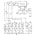
- the single figure in the drawing is a schematic circuit diagram of the regulating circuitry of the invention.
- a negative bias voltage, V BB is generated on the output conductor 10 of a charge pump circuit including the MOS transistors 12, 13, 14 and 15.
- the source element of transistor 12 is coupled to ground reference and the transistors 12,13 and 14 are connected in series so that the drain element of transistor 14 is connected to the output conductor 10.
- the gate elements of transistors 12, 13 and 14 are connected to their own drain elements and the series transistors 12 and 13 are shunted with the transistor 15, the source element of which is connected to ground reference and the gate and drain element of which is connected to the interconnection of transistors 13 and 14.
- Pumping action of the charge pump is under the control of an oscillator 16 that produces two oppositely phased signals through capacitors 18 and 20 to the gates of transistor 12 and 13, respectively.
- the regulation circuitry of the invention provides a relatively constant substrate bias voltage on the conductor 10 so that the static random access memory receiving the bias voltage will maintain a current necessary to prevent loss of the data stored therein.
- Oscillator 16 is inhibited or enabled by an over-current comparator, an under-current comparator and the enhancement transistor threshold substrate bias voltage sensor, the combined outputs of which are suitably gated to either inhibit or enable the oscillator 16. All transistors in the comparators and sensor are on the same substrate with the memory components and are therefore subjected to the same bias voltage.
- the over current comparator comprises transistors 22 through 27 and detects when the current through the memory load transistor is greater than the prescribed limit. When this occurs, the comparator generates a low oscillator enabling output signal into the conductor 28 which provides one input to the AND-gate 48.
- the under-current comparator comprising transistors 32 through 37 detects when the current through the memory load transistor is lower than the prescribed limit. When this occurs, the comparator generates a high output signal through conductor 38 into the NOR-gate 40 to thereby produce a low inhibiting signal into the oscillator 16 which, in turn, shuts off the charge pump and reduces the negative substrate bias voltage on the output conductor 10. As previously mentioned, the lower or less negative bias voltage in the random access memory permits an increased memory current for maintaining the data stored therein.
- the third regulation signal is provided by transistors 42 and 44 which produces a high output signal on the conductor 46 whenever the substrate bias is sufficient to turn off the transistor 44, the gate of which is held near the threshold.
- the memory power supply voltage conductor 50 may be either at the V cc voltage of the associated microcomputer employing the memory or may be at a standby voltage supplied, for example, by an external battery that is applied to the memory voltage conductor 50 whenever the computer system V cc is turned off.
- a suitable voltage must appear on the memory voltage conductor 50 as well as a proper substrate bias voltage on the conductor 10 in order to maintain the data stored in the memory.
- oscillator 16 and the associated gating circuits 40 and 48 are not operated directly from the system V cc but are connected for operation from the memory voltage conductor 50 so that their operation can be maintained during standby periods.
- the overcurrent comparator is a current mirror and includes MOS transistors 22 and 23 connected in series between conductor 50 and ground reference.
- Transistor 22 is a heavy depletion transistor, indicated by the solid triangle in the drawing, and is coupled between the memory voltage conductor 50 and the drain element of the enhancement transistor 23.
- the gate elements of transistors 22 and 23 are connected together and to their source-drain interconnection where a reference current is established that is mirrored into the following inverter circuit comprising transistors 24 and 25.
- the inverter circuit comprises transistors 24 and 25 in series.
- Transistor 24 is a light depletion transistor with its drain element connected to the memory voltage conductor 50 and its gate element connected to its source conductor, which point defines the output of the inverter.
- Enhancement transistor 25 is similar to the enhancement transistor 23 in the voltage divider pair 22 and 23 and the gate of transistor 25 is coupled to the output point at the interconnection of transistors 22 and 23.
- Light depletion enhancement transistor 24, indicated by the open triangle is physically constructed to be slightly shorter than the memory load transistor so that the transistor 24 may draw a slightly larger current than the predetermined norm for the memory transistor.
- Transistor pairs 22-23 and 24-25 comprise a current mirror wherein transistors 22 and 23 establish a reference current which is mirrored into the inverter pair.
- the light depletion load transistor 24 is capable of providing more than the demanded current through the inverter pair 24 and 25, then the voltage at the inverter output point 52 will be higher than the voltage at the divider output point 54 and will therefore exceed the threshold voltage necessary to turn on the enhancement transistor 27 in the subsequent inverter circuit. If the current through the transistor 24 is near its turnoff point, the voltage at point 52 will be low, therefore cutting off conduction through the transistor 27 in the inverter circuit.
- This inverter circuit includes a high depletion transistor 26 connected to the RAM voltage conductor 50 and the transistor 27 coupled between ground reference and the source element of transistor 26. The gate of transistor 27 is coupled to the output point 52 and the gate of transistor 26 is coupled to its source element and to the output conductor 28.
- output conductor 28 will carry a high signal if the current through the load depletion sampling transistor 24 and its associated enhancement transistor 25 is lower than the current established through the voltage divider pair comprising transistors 22 and 23. If the construction of a light depletion transistor 24 is such that it permits a current flow that exceeds that which is established at the output point 54, then the point 52 goes high to turn on transistor 27 and generate a low output on the conductor 28, thereby indicating excessive current through the memory load transistor.
- the comparator comprising transistors 32-37 is identical in construction and in operation with the comparator comprised of transistors 20 through 27 with the one exception that the light depletion transistor 34 is constructed to be slightly longer than the memory load transistor and therefore draws slightly less current. Therefore, when current through the memory load transistor is too low, there will be no current flow through transistor 34 and its associated enhancement transistor 35 so that the inverter transistor 37 will be non-conductive and a high output will be established on the conductor 38. A low input from conductor 38 into the NOR-gate 40 will inhibit operation of the oscillator 16 and its charge pump and the output voltage on conductor 10 will go in a positive direction. As previously mentioned, the lower negative bias voltage in the memory will result in a higher current through the memory transistors.
- a third control is provided by heavy depletion transistor 42 in series with the enhancement transistor 44.
- the drain of transistor 42 is connected to the memory voltage conductor 50 and the source of transistor 44 is connected to ground reference.
- a voltage divider comprising series resistors 56 and 58 in series between the memory voltage conductor 50 and ground reference establishes a fixed fraction of the memory voltage which is at the approximate threshold level and which is applied to the gate of the transistor 44. If the substrate bias voltage level is sufficiently negative to turn off the transistor 44, the high output voltage established at the interconnection of transistors 42 and 44 is carried by conductor 46 to provide one input to the AND-gate 48.
- an excessively high current through the memory transistor will result in conduction through transistor 24 and a low output on conductor 28.
- a sub-normal current through the memory transistor will result in a lack of current flow through the transistor 34 to produce a high output on the conductor 38.
- the level of substrate bias is monitored by the transistor 44 which is turned off to provide a high output on the conductor 46 when the substrate bias level becomes excessive.
- the low current sensor comprising transistors 32 through 37 will maintain the memory load current above a minimum necessary for maintaining stored data by disabling oscillator 16 thereby producing a more positive V BB output and an increased memory load current.
- Another condition for the substrate bias voltage is to keep the threshold voltage of enhancement transistor 44 in the proper range.
- This control is provided by the circuitry formed by the series resistors 56 and 58 and the inverter implemented by the transistors 42 and 44. If the threshold of transistor 44 is more positive than the voltage level provided by the resistor voltage divider, then the transistor 44 turns off and the output of the inverter applied to the AND-gate 48 will be high to disable the oscillator 16. If the output of the over-current sensor comprising transistors 22 through 27 is high indicating that the memory current does not exceed its upper limit, the output of AND-gate 48 will be high so that the oscillator 16 is disabled.
- the substrate bias voltage goes more and more positive until a level is reached at which the over-current sensor will switch its output to a low level, indicating an upper limit of memory load current.
- This low output signal from the over-current sensor will produce a low output of AND-gate 48 irrespective of the level at the output of the inverter circuit controlled by the condition of enhancement transistor 44. Therefore oscillator 16 becomes enabled and the substrate bias voltage goes more negative, resulting in lowering of the memory load current.
- the under-current sensor controls the most negative level of the substrate bias voltage by disabling the oscillator 16 to keep the memory alive; and the over-current sensor controls the most positive level of the substrate bias voltage by enabling the oscillator 16 even if the enhancement transistor threshold control circuit demands a more positive substrate voltage.
Landscapes
- Engineering & Computer Science (AREA)
- Power Engineering (AREA)
- Physics & Mathematics (AREA)
- Microelectronics & Electronic Packaging (AREA)
- Electromagnetism (AREA)
- Nonlinear Science (AREA)
- Computer Hardware Design (AREA)
- General Physics & Mathematics (AREA)
- Radar, Positioning & Navigation (AREA)
- Automation & Control Theory (AREA)
- Semiconductor Integrated Circuits (AREA)
- Dram (AREA)
- Static Random-Access Memory (AREA)
Description
- This invention relates to MOS microcomputer circuitry and particularly to MOS circuitry for regulating the level of substrate bias voltage applied to a static random access memory, hence maintaining the data sustaining current through the memory.
- Most modern integrated circuit microcomputers contain a random access memory designed to contain temporary data or instructions for operation of the microcomputer. The data stored in a static random access memory is destroyed or lost whenever the current through the memory drops below a minimum data sustaining level, and an excessive current through the memory load transistor affects the reliability of the memory by limiting the useful life of the transistor by over-heating. A proper load current is therefore necessary.
- The load current in a typical N-channel silicon gate MOS transistor circuit is determined by the threshold voltage of the depletion memory load transistor. A greater negative bias voltage increases the threshold voltage and results in lower load currents. Conversely, a more positive bias voltage decreases the threshold voltage and results in higher load current. For proper regulation of the memory load current, it is necessary to provide regulation of the bias voltage generating circuits.
- From "The Transactions of the IECE of Japan", vol. E 63, no. 7, Section E, July 1980, pages 520-525, Tokyo (JP), M. Morimoto et al "High speed DSA 4 Kbit static RAM" a MOS bias voltage regulating circuitry for establishing a predetermined substrate bias voltage level for an associated static random access memory is known, which regulating circuitry includes an oscillator for generating a pair of oppositely phased output signals and a charge pump coupled to said oscillator and responsive to said pair of output signals for generating the bias voltage output.
- The "IEEE Journal of Solid State Circuits", vol. SC-15, no. 5, October 1980, pages 820-826, New York (USA) W. L. Martino et al "An on-chip back bias generator for MOS dynamic memory" describes a MOS bias voltage generating circuitry for establishing a predetermined substrate bias voltage level for an associated dynamic random access memory, said regulating circuitry including an oscillator for generating a pair of oppositely phased output signals, a charge pump coupled to said oscillator and responsive to said pair of output signals for generating the bias voltage output, and control circuitry for controlling the operation of said oscillator, said control circuitry comprising bias voltage level sensing circuitry for generating an oscillator inhibiting signal when the substrate bias voltage level of said sensing circuitry and said memory exceeds a predetermined level.
- It is a general object of the present invention to provide proper bias regulation for a static random access memory so that a proper data-sustaining current through the memory is maintained.
- This and other objects are attained, in accordance with the invention, by MOS bias voltage regulating circuitry for establishing a predetermined substrate bias voltage level for an associated static random access memory, said regulating circuitry including an oscillator for generating a pair of oppositely phased output signals, a charge pump coupled to said oscillator and responsive to said pair of output signals for generating the bias voltage output, and control circuitry for controlling the operation of said oscillator, said control circuit comprising: under-current sensing circuitry for generating an oscillator inhibiting signal whenever the memory current drops below a predetermined level; bias voltage level sensing circuitry for generating a second oscillator inhibiting signal when the substrate bias voltage level of said sensing circuitry and said memory exceeds a predetermined level; and over-current sensing circuitry for generating an oscillator enabling signal whenever said memory current exceeds a predetermined level, said enabling signal controlling the operation of said oscillator irrespective of the existence of said second oscillator inhibiting signal.
- The single figure in the drawing is a schematic circuit diagram of the regulating circuitry of the invention.
- As illustrated in the circuitry of the drawing, a negative bias voltage, VBB, is generated on the
output conductor 10 of a charge pump circuit including theMOS transistors transistor 12 is coupled to ground reference and thetransistors transistor 14 is connected to theoutput conductor 10. The gate elements oftransistors series transistors transistor 15, the source element of which is connected to ground reference and the gate and drain element of which is connected to the interconnection oftransistors oscillator 16 that produces two oppositely phased signals throughcapacitors transistor oscillator 16 is functioning, the bias voltage onconductor 10 is driven more negatively; conversely, while theoscillator 16 is inhibited, the bias voltage onconductor 10 drops or goes less negative. The regulation circuitry of the invention provides a relatively constant substrate bias voltage on theconductor 10 so that the static random access memory receiving the bias voltage will maintain a current necessary to prevent loss of the data stored therein. -
Oscillator 16 is inhibited or enabled by an over-current comparator, an under-current comparator and the enhancement transistor threshold substrate bias voltage sensor, the combined outputs of which are suitably gated to either inhibit or enable theoscillator 16. All transistors in the comparators and sensor are on the same substrate with the memory components and are therefore subjected to the same bias voltage. - The over current comparator comprises
transistors 22 through 27 and detects when the current through the memory load transistor is greater than the prescribed limit. When this occurs, the comparator generates a low oscillator enabling output signal into theconductor 28 which provides one input to theAND-gate 48. - The under-current
comparator comprising transistors 32 through 37 detects when the current through the memory load transistor is lower than the prescribed limit. When this occurs, the comparator generates a high output signal throughconductor 38 into theNOR-gate 40 to thereby produce a low inhibiting signal into theoscillator 16 which, in turn, shuts off the charge pump and reduces the negative substrate bias voltage on theoutput conductor 10. As previously mentioned, the lower or less negative bias voltage in the random access memory permits an increased memory current for maintaining the data stored therein. The third regulation signal is provided bytransistors conductor 46 whenever the substrate bias is sufficient to turn off thetransistor 44, the gate of which is held near the threshold. - It should be noted that the memory power
supply voltage conductor 50 may be either at the V cc voltage of the associated microcomputer employing the memory or may be at a standby voltage supplied, for example, by an external battery that is applied to thememory voltage conductor 50 whenever the computer system Vcc is turned off. During periods that the V cc is turned off it is obvious that a suitable voltage must appear on thememory voltage conductor 50 as well as a proper substrate bias voltage on theconductor 10 in order to maintain the data stored in the memory. For this reason,oscillator 16 and the associatedgating circuits memory voltage conductor 50 so that their operation can be maintained during standby periods. - The overcurrent comparator is a current mirror and includes
MOS transistors conductor 50 and ground reference.Transistor 22 is a heavy depletion transistor, indicated by the solid triangle in the drawing, and is coupled between thememory voltage conductor 50 and the drain element of theenhancement transistor 23. The gate elements oftransistors circuit comprising transistors - The inverter circuit comprises
transistors Transistor 24 is a light depletion transistor with its drain element connected to thememory voltage conductor 50 and its gate element connected to its source conductor, which point defines the output of the inverter.Enhancement transistor 25 is similar to theenhancement transistor 23 in thevoltage divider pair transistor 25 is coupled to the output point at the interconnection oftransistors depletion enhancement transistor 24, indicated by the open triangle, is physically constructed to be slightly shorter than the memory load transistor so that thetransistor 24 may draw a slightly larger current than the predetermined norm for the memory transistor. Transistor pairs 22-23 and 24-25 comprise a current mirror whereintransistors depletion load transistor 24 is capable of providing more than the demanded current through theinverter pair inverter output point 52 will be higher than the voltage at thedivider output point 54 and will therefore exceed the threshold voltage necessary to turn on theenhancement transistor 27 in the subsequent inverter circuit. If the current through thetransistor 24 is near its turnoff point, the voltage atpoint 52 will be low, therefore cutting off conduction through thetransistor 27 in the inverter circuit. This inverter circuit includes ahigh depletion transistor 26 connected to theRAM voltage conductor 50 and thetransistor 27 coupled between ground reference and the source element oftransistor 26. The gate oftransistor 27 is coupled to theoutput point 52 and the gate oftransistor 26 is coupled to its source element and to theoutput conductor 28. - Very briefly reviewing,
output conductor 28 will carry a high signal if the current through the loaddepletion sampling transistor 24 and its associatedenhancement transistor 25 is lower than the current established through the voltage dividerpair comprising transistors light depletion transistor 24 is such that it permits a current flow that exceeds that which is established at theoutput point 54, then thepoint 52 goes high to turn ontransistor 27 and generate a low output on theconductor 28, thereby indicating excessive current through the memory load transistor. - The comparator comprising transistors 32-37 is identical in construction and in operation with the comparator comprised of
transistors 20 through 27 with the one exception that thelight depletion transistor 34 is constructed to be slightly longer than the memory load transistor and therefore draws slightly less current. Therefore, when current through the memory load transistor is too low, there will be no current flow throughtransistor 34 and its associatedenhancement transistor 35 so that theinverter transistor 37 will be non-conductive and a high output will be established on theconductor 38. A low input fromconductor 38 into theNOR-gate 40 will inhibit operation of theoscillator 16 and its charge pump and the output voltage onconductor 10 will go in a positive direction. As previously mentioned, the lower negative bias voltage in the memory will result in a higher current through the memory transistors. - A third control is provided by
heavy depletion transistor 42 in series with theenhancement transistor 44. The drain oftransistor 42 is connected to thememory voltage conductor 50 and the source oftransistor 44 is connected to ground reference. A voltage divider comprisingseries resistors memory voltage conductor 50 and ground reference establishes a fixed fraction of the memory voltage which is at the approximate threshold level and which is applied to the gate of thetransistor 44. If the substrate bias voltage level is sufficiently negative to turn off thetransistor 44, the high output voltage established at the interconnection oftransistors conductor 46 to provide one input to theAND-gate 48. - To summarize the operation of the three individual sensors: an excessively high current through the memory transistor will result in conduction through
transistor 24 and a low output onconductor 28. A sub-normal current through the memory transistor will result in a lack of current flow through thetransistor 34 to produce a high output on theconductor 38. The level of substrate bias is monitored by thetransistor 44 which is turned off to provide a high output on theconductor 46 when the substrate bias level becomes excessive. - In the operation of the sensors in a complete substrate bias voltage controller, the low current
sensor comprising transistors 32 through 37 will maintain the memory load current above a minimum necessary for maintaining stored data by disablingoscillator 16 thereby producing a more positive VBB output and an increased memory load current. - Another condition for the substrate bias voltage is to keep the threshold voltage of
enhancement transistor 44 in the proper range. This control is provided by the circuitry formed by theseries resistors transistors transistor 44 is more positive than the voltage level provided by the resistor voltage divider, then thetransistor 44 turns off and the output of the inverter applied to the AND-gate 48 will be high to disable theoscillator 16. If the output of the over-currentsensor comprising transistors 22 through 27 is high indicating that the memory current does not exceed its upper limit, the output of AND-gate 48 will be high so that theoscillator 16 is disabled. Now, the substrate bias voltage goes more and more positive until a level is reached at which the over-current sensor will switch its output to a low level, indicating an upper limit of memory load current. This low output signal from the over-current sensor will produce a low output of AND-gate 48 irrespective of the level at the output of the inverter circuit controlled by the condition ofenhancement transistor 44. Thereforeoscillator 16 becomes enabled and the substrate bias voltage goes more negative, resulting in lowering of the memory load current. - Thus, the under-current sensor controls the most negative level of the substrate bias voltage by disabling the
oscillator 16 to keep the memory alive; and the over-current sensor controls the most positive level of the substrate bias voltage by enabling theoscillator 16 even if the enhancement transistor threshold control circuit demands a more positive substrate voltage.
Claims (6)
Applications Claiming Priority (2)
| Application Number | Priority Date | Filing Date | Title |
|---|---|---|---|
| US06/203,183 US4322675A (en) | 1980-11-03 | 1980-11-03 | Regulated MOS substrate bias voltage generator for a static random access memory |
| US203183 | 1998-11-30 |
Publications (3)
| Publication Number | Publication Date |
|---|---|
| EP0051532A2 EP0051532A2 (en) | 1982-05-12 |
| EP0051532A3 EP0051532A3 (en) | 1983-08-03 |
| EP0051532B1 true EP0051532B1 (en) | 1986-03-12 |
Family
ID=22752859
Family Applications (1)
| Application Number | Title | Priority Date | Filing Date |
|---|---|---|---|
| EP81401719A Expired EP0051532B1 (en) | 1980-11-03 | 1981-10-28 | Regulated mos substrate bias voltage generator for a static random access memory |
Country Status (7)
| Country | Link |
|---|---|
| US (1) | US4322675A (en) |
| EP (1) | EP0051532B1 (en) |
| JP (1) | JPS57109360A (en) |
| AU (1) | AU7703981A (en) |
| BR (1) | BR8107081A (en) |
| CA (1) | CA1183951A (en) |
| DE (1) | DE3174080D1 (en) |
Families Citing this family (29)
| Publication number | Priority date | Publication date | Assignee | Title |
|---|---|---|---|---|
| US4739191A (en) * | 1981-04-27 | 1988-04-19 | Signetics Corporation | Depletion-mode FET for the regulation of the on-chip generated substrate bias voltage |
| US4403158A (en) * | 1981-05-15 | 1983-09-06 | Inmos Corporation | Two-way regulated substrate bias generator |
| JPS57199335A (en) * | 1981-06-02 | 1982-12-07 | Toshiba Corp | Generating circuit for substrate bias |
| US4438346A (en) | 1981-10-15 | 1984-03-20 | Advanced Micro Devices, Inc. | Regulated substrate bias generator for random access memory |
| US4439692A (en) * | 1981-12-07 | 1984-03-27 | Signetics Corporation | Feedback-controlled substrate bias generator |
| US4433253A (en) * | 1981-12-10 | 1984-02-21 | Standard Microsystems Corporation | Three-phase regulated high-voltage charge pump |
| US4580067A (en) * | 1982-12-28 | 1986-04-01 | Mostek Corporation | MOS dynamic load circuit for switching high voltages and adapted for use with high threshold transistors |
| US4612457A (en) * | 1983-06-27 | 1986-09-16 | Texas Instruments Incorporated | Current limiting output buffer for integrated circuit |
| US4585954A (en) * | 1983-07-08 | 1986-04-29 | Texas Instruments Incorporated | Substrate bias generator for dynamic RAM having variable pump current level |
| IT1220982B (en) * | 1983-11-30 | 1990-06-21 | Ates Componenti Elettron | CIRCUIT REGULATOR OF THE POLARIZATION VOLTAGE OF THE SUBSTRATE OF AN INTEGRATED CIRCUIT WITH FIELD-EFFECT TRANSISTORS |
| JPS60130157A (en) * | 1983-12-17 | 1985-07-11 | Sharp Corp | Monolithic semiconductor ic |
| US4628215A (en) * | 1984-09-17 | 1986-12-09 | Texas Instruments Incorporated | Drive circuit for substrate pump |
| US4656369A (en) * | 1984-09-17 | 1987-04-07 | Texas Instruments Incorporated | Ring oscillator substrate bias generator with precharge voltage feedback control |
| US4701637A (en) * | 1985-03-19 | 1987-10-20 | International Business Machines Corporation | Substrate bias generators |
| JPS6238591A (en) * | 1985-08-14 | 1987-02-19 | Fujitsu Ltd | Complementary semiconductor memory device |
| US4825142A (en) * | 1987-06-01 | 1989-04-25 | Texas Instruments Incorporated | CMOS substrate charge pump voltage regulator |
| IT1225608B (en) * | 1988-07-06 | 1990-11-22 | Sgs Thomson Microelectronics | ADJUSTMENT OF THE VOLTAGE PRODUCED BY A VOLTAGE MULTIPLIER. |
| JP2805991B2 (en) * | 1990-06-25 | 1998-09-30 | ソニー株式会社 | Substrate bias generation circuit |
| FR2668668B1 (en) * | 1990-10-30 | 1994-02-04 | Samsung Electronics Co Ltd | SUBSTRATE VOLTAGE GENERATOR FOR A SEMICONDUCTOR DEVICE. |
| US5162668A (en) * | 1990-12-14 | 1992-11-10 | International Business Machines Corporation | Small dropout on-chip voltage regulators with boosted power supply |
| KR950002015B1 (en) * | 1991-12-23 | 1995-03-08 | 삼성전자주식회사 | Electrostatic source generation circuit operated by one oscillator |
| US5260646A (en) * | 1991-12-23 | 1993-11-09 | Micron Technology, Inc. | Low power regulator for a voltage generator circuit |
| JP2560983B2 (en) * | 1993-06-30 | 1996-12-04 | 日本電気株式会社 | Semiconductor device |
| US5852737A (en) * | 1995-04-24 | 1998-12-22 | National Semiconductor Corporation | Method and apparatus for operating digital static CMOS components in a very low voltage mode during power-down |
| US5880593A (en) * | 1995-08-30 | 1999-03-09 | Micron Technology, Inc. | On-chip substrate regulator test mode |
| US6822470B2 (en) | 1995-08-30 | 2004-11-23 | Micron Technology, Inc. | On-chip substrate regulator test mode |
| US6496345B1 (en) * | 2000-10-10 | 2002-12-17 | National Semiconductor Corporation | Current regulation with low on resistance in overdriven mode |
| US7260731B1 (en) | 2000-10-23 | 2007-08-21 | Transmeta Corporation | Saving power when in or transitioning to a static mode of a processor |
| US6486727B1 (en) * | 2001-10-11 | 2002-11-26 | Pericom Semiconductor Corp. | Low-power substrate bias generator disabled by comparators for supply over-voltage protection and bias target voltage |
Family Cites Families (6)
| Publication number | Priority date | Publication date | Assignee | Title |
|---|---|---|---|---|
| US3794862A (en) * | 1972-04-05 | 1974-02-26 | Rockwell International Corp | Substrate bias circuit |
| US3806741A (en) * | 1972-05-17 | 1974-04-23 | Standard Microsyst Smc | Self-biasing technique for mos substrate voltage |
| US4049980A (en) * | 1976-04-26 | 1977-09-20 | Hewlett-Packard Company | IGFET threshold voltage compensator |
| US4115710A (en) * | 1976-12-27 | 1978-09-19 | Texas Instruments Incorporated | Substrate bias for MOS integrated circuit |
| US4142114A (en) * | 1977-07-18 | 1979-02-27 | Mostek Corporation | Integrated circuit with threshold regulation |
| US4229667A (en) * | 1978-08-23 | 1980-10-21 | Rockwell International Corporation | Voltage boosting substrate bias generator |
-
1980
- 1980-11-03 US US06/203,183 patent/US4322675A/en not_active Expired - Lifetime
-
1981
- 1981-10-28 EP EP81401719A patent/EP0051532B1/en not_active Expired
- 1981-10-28 DE DE8181401719T patent/DE3174080D1/en not_active Expired
- 1981-10-30 BR BR8107081A patent/BR8107081A/en unknown
- 1981-11-02 AU AU77039/81A patent/AU7703981A/en not_active Abandoned
- 1981-11-02 CA CA000389216A patent/CA1183951A/en not_active Expired
- 1981-11-04 JP JP56175836A patent/JPS57109360A/en active Pending
Non-Patent Citations (1)
| Title |
|---|
| THE TRANS. INST. ELECTR. COMM. ENG. JAPAN, vol. E63, no. 7, Section E, July 1980, pages 520-525, Tokyo (JP); M. MORIMOTO et al.: "High speed DSA 4 kbit static RAM". * |
Also Published As
| Publication number | Publication date |
|---|---|
| AU7703981A (en) | 1982-05-13 |
| EP0051532A3 (en) | 1983-08-03 |
| EP0051532A2 (en) | 1982-05-12 |
| CA1183951A (en) | 1985-03-12 |
| DE3174080D1 (en) | 1986-04-17 |
| US4322675A (en) | 1982-03-30 |
| JPS57109360A (en) | 1982-07-07 |
| BR8107081A (en) | 1982-07-20 |
Similar Documents
| Publication | Publication Date | Title |
|---|---|---|
| US4322675A (en) | Regulated MOS substrate bias voltage generator for a static random access memory | |
| EP0389566B1 (en) | Improved low power dual-mode cmos bias voltage generator | |
| EP1508078B1 (en) | Voltage regulator with dynamically boosted bias current | |
| US4794278A (en) | Stable substrate bias generator for MOS circuits | |
| US6091282A (en) | High voltage generating circuit for a semiconductor memory circuit | |
| US4224539A (en) | FET Voltage level detecting circuit | |
| US4384350A (en) | MOS Battery backup controller for microcomputer random access memory | |
| USRE38891E1 (en) | Programmable load transient compensator for reducing the transient response time to a load capable of operating at multiple power consumption levels | |
| US4874967A (en) | Low power voltage clamp circuit | |
| JPH0447591A (en) | Semiconductor integrated circuit device | |
| JPH05109288A (en) | Semiconductor integrated circuit | |
| JP2973063B2 (en) | Switch circuit | |
| US5260646A (en) | Low power regulator for a voltage generator circuit | |
| US5889431A (en) | Current mode transistor circuit method | |
| JPH0214814B2 (en) | ||
| US6798276B2 (en) | Reduced potential generation circuit operable at low power-supply potential | |
| US5629646A (en) | Apparatus and method for power reduction in dRAM units | |
| US6094395A (en) | Arrangement for controlling voltage generators in multi-voltage generator chips such as DRAMs | |
| KR19990022525A (en) | Voltage regulation circuit and its method | |
| US5721510A (en) | Semiconductor integrated circuit having a substrate back bias voltage generating circuit which is responsive to a power supply detection circuit | |
| US5889430A (en) | Current mode transistor circuit | |
| US6538417B2 (en) | Voltage regulating device and process | |
| US5493572A (en) | Semiconductor integrated circuit with voltage limiter having different output ranges for normal operation and performing of aging tests | |
| US6151230A (en) | Charge pump regulation circuit with overvoltage protection | |
| KR100350768B1 (en) | Internal voltage generator |
Legal Events
| Date | Code | Title | Description |
|---|---|---|---|
| PUAI | Public reference made under article 153(3) epc to a published international application that has entered the european phase |
Free format text: ORIGINAL CODE: 0009012 |
|
| AK | Designated contracting states |
Designated state(s): DE FR GB IT NL |
|
| PUAL | Search report despatched |
Free format text: ORIGINAL CODE: 0009013 |
|
| AK | Designated contracting states |
Designated state(s): DE FR GB IT NL |
|
| 17P | Request for examination filed |
Effective date: 19840120 |
|
| GRAA | (expected) grant |
Free format text: ORIGINAL CODE: 0009210 |
|
| ITF | It: translation for a ep patent filed | ||
| AK | Designated contracting states |
Kind code of ref document: B1 Designated state(s): DE FR GB IT NL |
|
| REF | Corresponds to: |
Ref document number: 3174080 Country of ref document: DE Date of ref document: 19860417 |
|
| ET | Fr: translation filed | ||
| PLBE | No opposition filed within time limit |
Free format text: ORIGINAL CODE: 0009261 |
|
| STAA | Information on the status of an ep patent application or granted ep patent |
Free format text: STATUS: NO OPPOSITION FILED WITHIN TIME LIMIT |
|
| 26N | No opposition filed | ||
| ITTA | It: last paid annual fee | ||
| PGFP | Annual fee paid to national office [announced via postgrant information from national office to epo] |
Ref country code: GB Payment date: 19930917 Year of fee payment: 13 |
|
| PGFP | Annual fee paid to national office [announced via postgrant information from national office to epo] |
Ref country code: FR Payment date: 19931013 Year of fee payment: 13 |
|
| PGFP | Annual fee paid to national office [announced via postgrant information from national office to epo] |
Ref country code: DE Payment date: 19931026 Year of fee payment: 13 |
|
| PGFP | Annual fee paid to national office [announced via postgrant information from national office to epo] |
Ref country code: NL Payment date: 19931031 Year of fee payment: 13 |
|
| PG25 | Lapsed in a contracting state [announced via postgrant information from national office to epo] |
Ref country code: GB Effective date: 19941028 |
|
| PG25 | Lapsed in a contracting state [announced via postgrant information from national office to epo] |
Ref country code: NL Effective date: 19950501 |
|
| NLV4 | Nl: lapsed or anulled due to non-payment of the annual fee | ||
| GBPC | Gb: european patent ceased through non-payment of renewal fee |
Effective date: 19941028 |
|
| PG25 | Lapsed in a contracting state [announced via postgrant information from national office to epo] |
Ref country code: FR Effective date: 19950630 |
|
| PG25 | Lapsed in a contracting state [announced via postgrant information from national office to epo] |
Ref country code: DE Effective date: 19950701 |
|
| REG | Reference to a national code |
Ref country code: FR Ref legal event code: ST |