EP0048933A1 - Circuit for correcting error in digital information signal - Google Patents
Circuit for correcting error in digital information signal Download PDFInfo
- Publication number
- EP0048933A1 EP0048933A1 EP81107526A EP81107526A EP0048933A1 EP 0048933 A1 EP0048933 A1 EP 0048933A1 EP 81107526 A EP81107526 A EP 81107526A EP 81107526 A EP81107526 A EP 81107526A EP 0048933 A1 EP0048933 A1 EP 0048933A1
- Authority
- EP
- European Patent Office
- Prior art keywords
- circuit
- signal
- correction
- error
- data
- Prior art date
- Legal status (The legal status is an assumption and is not a legal conclusion. Google has not performed a legal analysis and makes no representation as to the accuracy of the status listed.)
- Granted
Links
Images


Classifications
-
- H—ELECTRICITY
- H03—ELECTRONIC CIRCUITRY
- H03M—CODING; DECODING; CODE CONVERSION IN GENERAL
- H03M13/00—Coding, decoding or code conversion, for error detection or error correction; Coding theory basic assumptions; Coding bounds; Error probability evaluation methods; Channel models; Simulation or testing of codes
- H03M13/03—Error detection or forward error correction by redundancy in data representation, i.e. code words containing more digits than the source words
- H03M13/05—Error detection or forward error correction by redundancy in data representation, i.e. code words containing more digits than the source words using block codes, i.e. a predetermined number of check bits joined to a predetermined number of information bits
- H03M13/09—Error detection only, e.g. using cyclic redundancy check [CRC] codes or single parity bit
-
- G—PHYSICS
- G11—INFORMATION STORAGE
- G11B—INFORMATION STORAGE BASED ON RELATIVE MOVEMENT BETWEEN RECORD CARRIER AND TRANSDUCER
- G11B20/00—Signal processing not specific to the method of recording or reproducing; Circuits therefor
- G11B20/10—Digital recording or reproducing
- G11B20/18—Error detection or correction; Testing, e.g. of drop-outs
- G11B20/1806—Pulse code modulation systems for audio signals
- G11B20/1809—Pulse code modulation systems for audio signals by interleaving
Definitions
- This invention relates to circuits for correcting errors in digital information signals having been subjected to errors and time-base variations in a passage through a PCM audio equipment or other systems.
- the term "information signal” is intended to mean a signal which includes a plurality of digital signal trains and a sync signal in the form of recurrent sync pulses interposed between adjacent digital signal trains.
- the information signal having been subjected to time-base variations due to its passage through a system no longer has a constant sync signal period or sync pulse repetition period. Therefore, correction of errors produced in the digital data signal by means of adjacent code correction using error detection codes does not always yield satisfactory results. This is because of the fact that the time within the sync signal period, which is available for the error correction operation, varies and is liable to expire before the completion of all the steps of the error correction operation, as will be understood from the description later given.
- An object of the invention is to provide an improved circuit for correcting errors in a digital information signal containing errors and subjected to time-base variations.
- Another object of the invention is to provide an error correction circuit for a high quality PCM reproducing system, which can reduce or eliminate the generation of abnormal sound in playback with a PCM recorder by obviating erroneous correction of errors due to curtailed error correction operation caused by VTR jitter or the like.
- the state of a counter which is cleared by an error correction operation start signal synchronized with a sync pulse in the information signal and which provides a basic timing for the error correction operation, is decoded to determine or monitor whether or not the error correction operation started with the appearance of the error correction operation start signal has been completed at the time of the appearance of the next start signal, and the output of the result of the error correction operation is inhibited if the operation is not completed by the time of appearance of the next start signal.
- the data the correction of which is incomplete (and which remains in a storage device) is provided with an error flag, so that such correction as the previous value holding or interpolation can be made using this flag before delivering the corresponding reproduced output.
- data blocks each of which consists of 6 interleaved sampled signal words (hereinafter referred to as information data) and two error correction words (hereinafter referred to as error correction data) P and Q, are monitored by using an error detection word (hereinafter referred to as CRC) for every horizontal scanning period in the playback with the VTR, and are transferred to a de-interleaving RAM with an error flag attached to error data.
- CRC error detection word
- the data read out from the RAM is not directly coupled to a D-A converter but is subjected to error correction, and the results of the correction is written again in the RAM.
- the corrected data is thus supplied to the D-A converter.
- Fig. 1 is a block diagram of a PCM recorder. A portion enclosed by a chain line corresponds to an encoder/decoder for effecting digital signal processing.
- the function of the PCM recorder is roughly as follows:
- This portion of the recorder time-divides a two-channel (L- and R-channel) audio signal input and converts the individual signal divisions to 14-bit digital signals (words) in terms of "1" and "0".
- Six words (three L-channel and three R-channel signals alternately arranged) each having a 14-bit configuration constitute one block.
- Error correction words P and Q are generated through exclusive ORing and matrix operation of the data of the L- and R-channel words (6 words).
- Continuously generated data are interleaved in a storage device in order to prevent generation of a burst error due to a large drop-out and improve the error correction efficiency.
- Error detection words (CRCC of 16 bits) are generated from the interleaved 8-words digital signal.
- VTR sync signal synchronized with these digital signals is generated, and these digital signals and VTR sync signal thus generated are converted into a video signal conforming to a standard VTR signal suited for recording with the VTR.
- the video signal reproduced from the VTR is separated into the sync signal and data signal and converted to the digital signals again.
- Error check of the reproduced data is done using the error detection words (CRCC), and error data is given an error flag for subsequent error correction.
- CRCC error detection words
- the interleaved data are re-arranged to the original order (i.e., de-interleaved), while at the same time wows and flutters due to the VTR rotation fluctuations are absorbed and removed.
- the digital signal in terms of "1” and “0” is converted to the audio signal, and also this audio signal is separated into the two-channel (L- and R-channel) signals.
- an error correction circuit In the PCM recorder shown in Fig. 1, errors occur in the information data of the reproduced signal due to dropouts caused by noise, foreign particles on and defects of the magnetic head and the magnetic surface of the magnetic tape in the recording system. To minimize the errors, an error correction circuit is provided. This error correction circuit effects error correction by making use of the error correction words.
- the error correction words are generated as and
- the symbol ⁇ signifies the modulo 2 summing or exclusive OR operation for the corresponding bits of the six individual words
- T signifies a 14-by-14-bit matrix called an auxiliary matrix.
- the hardware for the correction operation is thus constructed with circuits for generation of SP, generation of SQ, Tn multiplication operation and matrix multiplication by (T i-j ⁇ I) -1 .
- Such a circuitry itself is irrelevant to the subject matter of the invention, and it will be described hereinafter only briefly with reference to the drawings.
- Fig. 2 shows a flow chart of the error correction operation performed in the error correction circuit in Fig. 1.
- the correction operation is carried out as separate operations during a time period longer than one horizontal sync period as described in, for instance, Japanese Patent Application No. 132869/1980 (filed on September 26, 1980).
- the correction operation is carried out as separate operations Cl and C2 as shown in the flow chart of Fig. 2. These operations are carried out in consecutive horizontal sync periods.
- the results of the operation Cl is latched, and the operation C2 is carried out in the next horizontal sync period.
- the operation Cl is started after the latching of the result of the operation Cl.
- Fig. 3 is a block diagram showing an embodiment of the invention. The operation of this embodiment is described hereinunder in connection with Figs. 1 and 2, but the system, through which the information signal passes, is not limited to the VTR.
- the signal which can be processed by the error correction circuit according to the invention may be any digital information signal having passed through a system, which causes information errors and time-base variations.
- reference numeral 10 designates a reproducing system, which may be the VTR shown in Fig. 1.
- the digital information signal reproduced in the reproducing system 10 usually has a plurality of digital information signal trains respectively containing digital information data and error correction data and recurrent sync pulses inserted between adjacent signal trains.
- the digital information data-in the information signal contains errors due to dropouts as mentioned earlier and also has been subjected to the influence of time-base variations in passing through the system 10.
- This information signal is coupled through a sync/data separation circuit 11, and a sync signal or a signal generated in synchronism therewith are fed to a counter 1 as a correction operation start signal.
- a clock pulse signal at a predetermined repetition frequency is supplied from a clock source 9 to the counter 1.
- the counter 1 When it receives a correction operation start signal, the counter 1 starts to count clock pulses from the clock source 9, and continues counting immediately before the impression of the next sync signal or a correction operation start signal generated in synchronism therewith. With the impression of the start signal, it is reset and starts the counting of clock pulses afresh from zero.
- the output of the counter 1 is fed to a timing generator 3, which generates a timing signal according to the output of the counter 1.
- An error detection circuit 12 is effective to the invention in case where errors are contained in two words among the digital information words (for instance 6 words each of .14 bits) in a digital signal train, and it serves to detect the number of errors, for instance, by setting an error flag with respect to digital information where an error word is present. Where the circuit 12 is provided, digital information signal inclusive of the error number data is stored.
- a first operation circuit 4, a latch circuit 5 and a second operation circuit 6 are timed with the timing signal supplied from the timing generator 3.
- An error correction operation monitoring circuit 2 receives the output from the counter 1 and also the output from the error detection circuit 12 (if this circuit is employed), and its output is supplied to the writing control circuit 7.
- the error correction operation monitoring circuit 2 has a function of monitoring the number of operation steps executed in one sync signal period by making use of the output of the counter 1, i.e., a function of monitoring the extent of progress of operation or the degree of execution of operation steps.
- the second operation circuit 6 performs operation with the operation results from the first operation circuit 4.
- the number given on the right-hand side of the individual operation routines indicate the number of steps involved in the execution of the routines, i.e., they correspond to the numbers of timing pulses supplied from the timing generator 3 shown in Fig. 3.
- the content of the operation procedure shown in Fig. 2 and the step numbers involved are thus subject to changes whenever measures involved in the method of error correction such as error correction data are changed or modified.
- the operation of the embodiment will now be described with reference to Figs. 2 through 4.
- the operation Cl includes 14 steps, while the operation C2 includes 18 steps.
- the counter 1 is a circuit, which is cleared by an error correction operation start signal and counts 18 steps, and the error correction operation is performed with the timing of the output of the counter 1 and in the manner as shown in Fig. 2. Where the operations Cl and C2 are separately performed in the respective two sync signal periods, these operations Cl and C2 can proceed concurrently with respect to respective two adjacent data blocks.
- the operation Cl is completed with the. completion of the 14-th step from the appearance of the error correction operation start signal, while the operation C2 is completed with the completion of the 18-th step.
- the writing of the operation results of the correction operation circuitry 4 to 6 in the second storage section of the storage device 8 is controlled through the control circuit 7 in dependence upon the extent of contraction in the manner as described hereinafter.
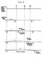
- the monitoring circuit 2 detects that the output of the counter 1, i.e., the number of operation steps executed by, for example, the first operation circuit 4, is less than 7. In this case, the error correction is impossible irrespective of whether one data block contains only one error word or two or more error words, so that the writing of the operation results in the storage device 8 under the control of the writing control circuit 7 is inhibited.
- the monitoring circuit 2 detects that the number of operation steps executed by, for example, the first operation circuit 4 during the period T h is equal to or greater than 7 and less than 14. In this case, if one data block contains only a single error word, the writing of the correct data of w i for the error data in the storage device 8 in a proper timing is allowed. If one data block contains two or more error words, the correction is impossible, so that the writing is inhibited as in the case of the signal S 2 . With a reproduced sync signal as shown at S 3 in Fig.
- the number of operation steps executed by, for example, the first operation circuit 4 during the period Th is equal to or greater than time period for 14 steps and less than time period for 30 steps.
- the writing of the correct data of w for the error word in the storage device 8 in a proper timing is allowed. If one block data containes two error words, error correction using error correction words P and Q is possible since the number of operation steps executed is equal to or greater than 14.
- the operation results so far are latched in the latch circuit 5, the remaining operation is performed in, for example, the second operation circuit 6 from the instant of start of the next sync signal period, and the writing of the correct data of w i and w. for the error words which are the final results of operation in the storage device 8 is allowed.
- a reproduced sync signal as shown at S 4 in Fig. 4 (with the period T h being longer than or equal to time period for 30 steps), it is detected that all the operation steps have been executed in, for example, the first operation circuit 4, so that the writing of the correct data of w. for the one error word or of w. and w j for the two error words in a proper timing is allowed.
- the first operation circuit 4 executes only the steps that can be executed within a first sync signal period T h among the operation steps shown in Fig. 2.
- the results of operation are latched in the second operation circuit 6, and the remaining operation steps are executed in the second operation circuit 6 during the second sync signal period (following the first).
- the above control has an effect of preventing the writing of erroneous error correction data in the storage device 8 that might otherwise result from the lack of execution of the correction operation steps.
- concealment of the reproduced, read-out output from the storage device 8 is effected by previous value holding or interpolation or substituting an average value of-the preceding and succeeding data using a flag set in the RAM 8 in accordance with the result of error detection before the execution of the correction operation. This prevents the generation of abnormal sound due to the output of erroneous correction data.
- Fig. 5 shows an example of a construction and arrangement of the first operation circuit 4, latch circuit 5 and second operation circuit 6 shown in Fig. 3.
- This circuit effects the operation of correcting errors occurring in the PCM recorder of Fig. 1 according to the error correction operation program shown in Fig. 2.
- the construction is thus irrelevant to the subject matter of the invention, and it will be described only briefly.
- An SP latch circuit 41 is constituted by, for instance, 14 unit circuits each including a two-input exclusive OR gate and a latch circuit connected to the output of the gate. In each unit circuit, a data word bit of the information signal read out from the storage device 8 is coupled to one of the input terminals of the gate, and the output of the latch circuit is coupled to the other gate input terminal.
- SP w I ⁇ w 2 ⁇ ... w 6 0 P is calculated and latched in the SP latch circuit 41.
- a T -7 -multiplication circuit 42 which receives the data word bits from the storage device 8, cooperates with a T-multiplication circuit 43 and SQ latch circuit 44 to cause an SQ latch circuit 44 to generate T i-7 SP ⁇ SQ.
- the SQ latch circuit 44 includes unit circuits each having a two-input exclusive OR gate and a latch circuit connected to the output of the gate.
- the output of the latch circuit is coupled to the T-multiplication circuit 43.
- One input terminal of the gate is connected with the output of the T -7 - multiplication circuit 42 while the other input terminal of the gate is connected with the output of the T-multiplication circuit 43 in each unit circuit though not shown in detail.
- the outputs of the T -7 and T multiplication circuits 42 and 43 and of the SP latch circuit 41 are selectively supplied to the SQ latch circuit 44 through a selector 45, thereby generating the above- mentioned T i-7 SQ ⁇ SP.
- a matrix ROM 46 has a 14-by-14-bit construction generates (T i-j ⁇ I) -1 .
- the outputs of the w. and w i latch circuits 48 and 50 are supplied to the writing control circuit 7.
- Fig. 6 shows an example of a construction and arrangement of the error correction operation monitoring circuit 2 and writing control circuit 7.
- the monitoring circuit 2 includes an n-bit latch circuit 21 receiving the output of the counter 1, a comparing circuit 22 for comparing the output of the n-bit latch circuit 21 with reference values representing a plurality of critical steps required in the error correction operation (last steps in such operations of a minimum number of steps necessary for the correction of a single error word or two error words such as the 7-th step or 14-th step in Fig. 2), and a flag counter 23 for counting an error flag signals supplied from the error correction circuit 12.
- the n-bit latch circuit 21 latches the count value of the counter 1 immediately before the counter 1 is reset by each sync pulse.
- the comparing circuit 22 includes means for generating a signal r 1 which is "1" when the output of the n-bit latch circuit 21 is less than the reference value representing the seventh step, means for generating a signal r 2 which is “1” when the latch circuit output is equal to or greater than the reference value for the seventh step and less than a reference value for the 14-th step, and means for generating a signal r 3 which is "1" when the latch circuit output is equal to or greater than the reference value for the 14-th step.
- the flag counter 23 generates a signal f 1 which is "1" when one digital data block contains only a single error word and a signal f 2 which is "1" when one digital data block contains two error words.
- the writing control circuit 7 includes a logic circuit 71 which receives the outputs r l , r 2 and r 3 of the comparing circuit 22 in the monitoring circuit 2 and the outputs f 1 and f 2 of the flag counter 23, and a gate circuit 72 which receives the outputs m 1 , m 2 and m 3 of the logic circuit 71. To the gate circuit 72 are also supplied the outputs w i and w. of the operation circuit such as shown in Fig. 5.
- the logic circuit 71 includes a two-input OR gate receiving the outputs f 1 and f 2 of the flag counter 23, a two-input AND gate receiving the output r 1 of the comparing circuit 22 and the output of the OR gate and generating a control signal m 1 for allowing the writing of w i and w., a two-input AND gate receiving the output r 2 of the comparing circuit 22 and output f 1 of the flag counter 23 and generating a control signal m 2 allowing the writing of w i , a two-input AND gate receiving the output r 2 of the comparing circuit 22 and output f 2 of the flag counter 23 and generating a control signal m 3 for inhibiting the writing, and means for providing the output r 3 of the comparing circuit 22 as a writing inhibition control signal m 4 .
- a gate circuit 72 receives the control signals m 1 to m 4 from the logic circuit 71 and controls the writing into the storage device (RAM) 8 by gating the signals w i and w j from the operation circuit shown in Fig. 5 according to the received control signals.
Abstract
Description
- This invention relates to circuits for correcting errors in digital information signals having been subjected to errors and time-base variations in a passage through a PCM audio equipment or other systems.
- Throughout the specification, the term "information signal" is intended to mean a signal which includes a plurality of digital signal trains and a sync signal in the form of recurrent sync pulses interposed between adjacent digital signal trains. The information signal having been subjected to time-base variations due to its passage through a system no longer has a constant sync signal period or sync pulse repetition period. Therefore, correction of errors produced in the digital data signal by means of adjacent code correction using error detection codes does not always yield satisfactory results. This is because of the fact that the time within the sync signal period, which is available for the error correction operation, varies and is liable to expire before the completion of all the steps of the error correction operation, as will be understood from the description later given.
- An object of the invention is to provide an improved circuit for correcting errors in a digital information signal containing errors and subjected to time-base variations.
- Another object of the invention is to provide an error correction circuit for a high quality PCM reproducing system, which can reduce or eliminate the generation of abnormal sound in playback with a PCM recorder by obviating erroneous correction of errors due to curtailed error correction operation caused by VTR jitter or the like.
- According to the invention, the state of a counter, which is cleared by an error correction operation start signal synchronized with a sync pulse in the information signal and which provides a basic timing for the error correction operation, is decoded to determine or monitor whether or not the error correction operation started with the appearance of the error correction operation start signal has been completed at the time of the appearance of the next start signal, and the output of the result of the error correction operation is inhibited if the operation is not completed by the time of appearance of the next start signal. In such a case, the data, the correction of which is incomplete (and which remains in a storage device), is provided with an error flag, so that such correction as the previous value holding or interpolation can be made using this flag before delivering the corresponding reproduced output.
- Now, the invention will be described by way of exemplified embodiments with reference to the accompanying drawings, in which:
- Fig. 1 is a block diagram showing a PCM recorder, to which the invention is applicable;
- Fig. 2 is a flow chart of an operation routine necessary for correcting data errors produced in the PCM recorder of Fig. 1;
- Fig. 3 is a block diagram showing an embodiment of the invention;
- Fig. 4 is a view useful to explain the operation of the embodiment of Fig. 3;
- Fig. 5 is a block diagram showing an example of an operation circuit in the embodiment of Fig. 3; and
- Fig. 6 is a block diagram showing an example of an error correction operation monitoring circuit and a writing control circuit that may be used for the embodiment of Fig. 3.
- Now, the state of art, to which the invention pertains, will be described in connection with a home- use PCM encoder/decoder for recording and reproducing. audio signals on the basis of the general standard in Japan for the sake of simplicity. The system, through which the information signal passes, thus corresponds to a VTR here. The standard is announced as the Technical File STC-007 of Electronic Industries Association of Japan (EIAJ), June 1, 1979, and reported in "NIKKEI ELECTRONICS", June 20, 1979, pp. 185-200 and "DEMPA KAGAKU" (or "Electromagnetic Wave Science"), September, 1979, pp. 218-220. In the PCM signal processing system conforming to the general standard, data blocks, each of which consists of 6 interleaved sampled signal words (hereinafter referred to as information data) and two error correction words (hereinafter referred to as error correction data) P and Q, are monitored by using an error detection word (hereinafter referred to as CRC) for every horizontal scanning period in the playback with the VTR, and are transferred to a de-interleaving RAM with an error flag attached to error data. The data read out from the RAM is not directly coupled to a D-A converter but is subjected to error correction, and the results of the correction is written again in the RAM. The corrected data is thus supplied to the D-A converter.
- Fig. 1 is a block diagram of a PCM recorder. A portion enclosed by a chain line corresponds to an encoder/decoder for effecting digital signal processing. The function of the PCM recorder is roughly as follows:
- This portion of the recorder time-divides a two-channel (L- and R-channel) audio signal input and converts the individual signal divisions to 14-bit digital signals (words) in terms of "1" and "0". Six words (three L-channel and three R-channel signals alternately arranged) each having a 14-bit configuration constitute one block.
- Error correction words P and Q are generated through exclusive ORing and matrix operation of the data of the L- and R-channel words (6 words).
- Continuously generated data are interleaved in a storage device in order to prevent generation of a burst error due to a large drop-out and improve the error correction efficiency.
- Error detection words (CRCC of 16 bits) are generated from the interleaved 8-words digital signal.
- A VTR sync signal synchronized with these digital signals is generated, and these digital signals and VTR sync signal thus generated are converted into a video signal conforming to a standard VTR signal suited for recording with the VTR.
- The video signal reproduced from the VTR is separated into the sync signal and data signal and converted to the digital signals again.
- Error check of the reproduced data is done using the error detection words (CRCC), and error data is given an error flag for subsequent error correction.
- Converse to the recording system storage device the interleaved data are re-arranged to the original order (i.e., de-interleaved), while at the same time wows and flutters due to the VTR rotation fluctuations are absorbed and removed.
- If the de-interleaved data is erroneous, error correction operation using the two error correction words P and Q is effected to recover the original correct data.
- The digital signal in terms of "1" and "0" is converted to the audio signal, and also this audio signal is separated into the two-channel (L- and R-channel) signals.
- In the PCM recorder shown in Fig. 1, errors occur in the information data of the reproduced signal due to dropouts caused by noise, foreign particles on and defects of the magnetic head and the magnetic surface of the magnetic tape in the recording system. To minimize the errors, an error correction circuit is provided. This error correction circuit effects error correction by making use of the error correction words.
- The principle underlying the generation of the error correction words and error correction using these error correction words are described in "NIKKEI ELECTRONICS", August 20, 1979, pp. 194-196, and will be summarized hereinbelow.
- Denoting 6 words constituting digital information data by w1, w2' ..., w6, the error correction words are generated as


modulo 2 summing or exclusive OR operation for the corresponding bits of the six individual words, and T signifies a 14-by-14-bit matrix called an auxiliary matrix. When it is detected that errors are contained in words w. and wj in one data block w1-w6, wi and wj are obtained from two-unknown, first-order simultaneous equations

condition 1 ≤ i ≤ j ≤ 6, and

- The hardware for the correction operation is thus constructed with circuits for generation of SP, generation of SQ, Tn multiplication operation and matrix multiplication by (Ti-j ⊕ I)-1. Such a circuitry itself, however, is irrelevant to the subject matter of the invention, and it will be described hereinafter only briefly with reference to the drawings.
- Fig. 2 shows a flow chart of the error correction operation performed in the error correction circuit in Fig. 1. Where the operation from the reading of data words till the writing of the error correction result is carried out in one horizontal sync period, it is likely to occur that the correction operation is not completely performed due to reduction of the horizontal sync period caused by jitter in the VTR. Accordingly, it has been proposed to carry out the correction operation as separate operations during a time period longer than one horizontal sync period as described in, for instance, Japanese Patent Application No. 132869/1980 (filed on September 26, 1980). As an example, the correction operation is carried out as separate operations Cl and C2 as shown in the flow chart of Fig. 2. These operations are carried out in consecutive horizontal sync periods. The results of the operation Cl is latched, and the operation C2 is carried out in the next horizontal sync period. The operation Cl is started after the latching of the result of the operation Cl.
- If the horizontal sync period is reduced and ended, due to the effect of jitter, before the completion of the operation Cl so that the operation C2 is started with the result of the operation Cl latched while the operation Cl is incomplete, erroneous correction is made with erroneous latched data. The result of the erroneous correction of the error data is written in the RAM or the storage device and is provided as the output signal. Since the error correction is carried out by using the Q code, the erroneously corrected data is likely to appear as audio data over the entire amplitude range and, when provided as the output signal to the D-A converter, will cause abnormal sound.
- Fig. 3 is a block diagram showing an embodiment of the invention. The operation of this embodiment is described hereinunder in connection with Figs. 1 and 2, but the system, through which the information signal passes, is not limited to the VTR. In general, the signal which can be processed by the error correction circuit according to the invention, may be any digital information signal having passed through a system, which causes information errors and time-base variations.
- Referring to Fig. 3,
reference numeral 10 designates a reproducing system, which may be the VTR shown in Fig. 1. The digital information signal reproduced in the reproducingsystem 10, usually has a plurality of digital information signal trains respectively containing digital information data and error correction data and recurrent sync pulses inserted between adjacent signal trains. The digital information data-in the information signal contains errors due to dropouts as mentioned earlier and also has been subjected to the influence of time-base variations in passing through thesystem 10. This information signal is coupled through a sync/data separation circuit 11, and a sync signal or a signal generated in synchronism therewith are fed to acounter 1 as a correction operation start signal. A clock pulse signal at a predetermined repetition frequency is supplied from aclock source 9 to thecounter 1. When it receives a correction operation start signal, thecounter 1 starts to count clock pulses from theclock source 9, and continues counting immediately before the impression of the next sync signal or a correction operation start signal generated in synchronism therewith. With the impression of the start signal, it is reset and starts the counting of clock pulses afresh from zero. The output of thecounter 1 is fed to atiming generator 3, which generates a timing signal according to the output of thecounter 1. - The information signal provided from the sync/data separation circuit 11, now free from the sync signal, is fed to a
storage device 8 and stored in a first storage section therein. Anerror detection circuit 12 is effective to the invention in case where errors are contained in two words among the digital information words (forinstance 6 words each of .14 bits) in a digital signal train, and it serves to detect the number of errors, for instance, by setting an error flag with respect to digital information where an error word is present. Where thecircuit 12 is provided, digital information signal inclusive of the error number data is stored. Afirst operation circuit 4, alatch circuit 5 and asecond operation circuit 6 are timed with the timing signal supplied from thetiming generator 3. These circuits serve to read out the information signal containing error, stored in the first storage section of the storage device (RAM) 8, latch the previous operation results in thelatch circuit 5, effect the remaining operation on the basis of the latched operation results and store the final results in a second storage section of thestorage device 8. The writing of the final operation results is controlled by awriting control section 7. An error correctionoperation monitoring circuit 2 receives the output from thecounter 1 and also the output from the error detection circuit 12 (if this circuit is employed), and its output is supplied to thewriting control circuit 7. The error correctionoperation monitoring circuit 2 has a function of monitoring the number of operation steps executed in one sync signal period by making use of the output of thecounter 1, i.e., a function of monitoring the extent of progress of operation or the degree of execution of operation steps. Thesecond operation circuit 6 performs operation with the operation results from thefirst operation circuit 4. - In Fig. 2, the number given on the right-hand side of the individual operation routines indicate the number of steps involved in the execution of the routines, i.e., they correspond to the numbers of timing pulses supplied from the
timing generator 3 shown in Fig. 3. The content of the operation procedure shown in Fig. 2 and the step numbers involved are thus subject to changes whenever measures involved in the method of error correction such as error correction data are changed or modified. The operation of the embodiment will now be described with reference to Figs. 2 through 4. - The operation Cl includes 14 steps, while the operation C2 includes 18 steps. The
counter 1 is a circuit, which is cleared by an error correction operation start signal and counts 18 steps, and the error correction operation is performed with the timing of the output of thecounter 1 and in the manner as shown in Fig. 2. Where the operations Cl and C2 are separately performed in the respective two sync signal periods, these operations Cl and C2 can proceed concurrently with respect to respective two adjacent data blocks. The operation Cl is completed with the. completion of the 14-th step from the appearance of the error correction operation start signal, while the operation C2 is completed with the completion of the 18-th step. When only a single error is contained and can be corrected with the sole P code by making use of the error detection code, it is only necessary for the correction to perform or execute 1-7 steps of the operation Cl to generate SP in one sync signal period. (In this case, all the error data have been stored as "0" in the RAM.) - If the sync signal period Th, i.e., the recurrence period of the correction operation start signals, is contracted due to the effect of jitter or the like, the writing of the operation results of the
correction operation circuitry 4 to 6 in the second storage section of thestorage device 8 is controlled through thecontrol circuit 7 in dependence upon the extent of contraction in the manner as described hereinafter. - With reproduced sync signal as shown at S1 in Fig. 4 (with the sync signal period Th being shorter than time period for 7 steps), the
monitoring circuit 2 detects that the output of thecounter 1, i.e., the number of operation steps executed by, for example, thefirst operation circuit 4, is less than 7. In this case, the error correction is impossible irrespective of whether one data block contains only one error word or two or more error words, so that the writing of the operation results in thestorage device 8 under the control of thewriting control circuit 7 is inhibited. With a reproduced sync signal shown at S2 in Fig. 4 (with the period Th being equal to or longer than time period for 7 steps and shorter than time period for 14 steps), themonitoring circuit 2 detects that the number of operation steps executed by, for example, thefirst operation circuit 4 during the period Th is equal to or greater than 7 and less than 14. In this case, if one data block contains only a single error word, the writing of the correct data of wi for the error data in thestorage device 8 in a proper timing is allowed. If one data block contains two or more error words, the correction is impossible, so that the writing is inhibited as in the case of the signal S2. With a reproduced sync signal as shown at S3 in Fig. 4 (with the signal period Th being equal to or longer than time period for 14 steps and shorter than time period for 30 steps), it is detected that the number of operation steps executed by, for example, thefirst operation circuit 4 during the period Th is equal to or greater than time period for 14 steps and less than time period for 30 steps. In this case, if one data block contains only a single error word, the writing of the correct data of w for the error word in thestorage device 8 in a proper timing is allowed. If one block data containes two error words, error correction using error correction words P and Q is possible since the number of operation steps executed is equal to or greater than 14. If this is the case, the operation results so far are latched in thelatch circuit 5, the remaining operation is performed in, for example, thesecond operation circuit 6 from the instant of start of the next sync signal period, and the writing of the correct data of wi and w. for the error words which are the final results of operation in thestorage device 8 is allowed. With a reproduced sync signal as shown at S4 in Fig. 4 (with the period Th being longer than or equal to time period for 30 steps), it is detected that all the operation steps have been executed in, for example, thefirst operation circuit 4, so that the writing of the correct data of w. for the one error word or of w. and wj for the two error words in a proper timing is allowed. It is to be understood that thefirst operation circuit 4 executes only the steps that can be executed within a first sync signal period Th among the operation steps shown in Fig. 2. The results of operation are latched in thesecond operation circuit 6, and the remaining operation steps are executed in thesecond operation circuit 6 during the second sync signal period (following the first). - The above control has an effect of preventing the writing of erroneous error correction data in the
storage device 8 that might otherwise result from the lack of execution of the correction operation steps. In case writing of corrected data in thestorage device 8 is not effected due to the lack of the execution of the correction operation steps, concealment of the reproduced, read-out output from thestorage device 8 is effected by previous value holding or interpolation or substituting an average value of-the preceding and succeeding data using a flag set in theRAM 8 in accordance with the result of error detection before the execution of the correction operation. This prevents the generation of abnormal sound due to the output of erroneous correction data. In the actual playback, the cases of correcting a single error word are overwhelmingly frequent compared to the cases where the correction of two error words is necessary. According to the instant embodiment, stronger protection is given to the case of correcting a single error word than to the case of correcting two error words with respect to the reduction of the operation period. Thus, the operation results are not unnecessarily left unused. - In the PCM signal recording and reproducing system in which analog audio signals are recorded and reproduced as digital signals, the generation of click noise is very detestable. Click noise may result from the erroneous correction of error data. With the instant embodiment, the probability of erroneous correction can be greatly reduced. Thus, steady and high quality sound reproduction can be obtainable even with a VTR, in which the tape has an unsatisfactory magnetic surface or the rotational drive mechanism is imperfect.
- Fig. 5 shows an example of a construction and arrangement of the
first operation circuit 4,latch circuit 5 andsecond operation circuit 6 shown in Fig. 3. This circuit effects the operation of correcting errors occurring in the PCM recorder of Fig. 1 according to the error correction operation program shown in Fig. 2. The construction is thus irrelevant to the subject matter of the invention, and it will be described only briefly. - An
SP latch circuit 41 is constituted by, for instance, 14 unit circuits each including a two-input exclusive OR gate and a latch circuit connected to the output of the gate. In each unit circuit, a data word bit of the information signal read out from thestorage device 8 is coupled to one of the input terminals of the gate, and the output of the latch circuit is coupled to the other gate input terminal. With this construction, SP = wI ⊕ w2 ⊕ ... w6 0 P is calculated and latched in theSP latch circuit 41. A T-7-multiplication circuit 42, which receives the data word bits from thestorage device 8, cooperates with a T-multiplication circuit 43 andSQ latch circuit 44 to cause anSQ latch circuit 44 to generate Ti-7 SP ⊕ SQ. TheSQ latch circuit 44 includes unit circuits each having a two-input exclusive OR gate and a latch circuit connected to the output of the gate. The output of the latch circuit is coupled to the T-multiplication circuit 43. One input terminal of the gate is connected with the output of the T-7-multiplication circuit 42 while the other input terminal of the gate is connected with the output of the T-multiplication circuit 43 in each unit circuit though not shown in detail. The outputs of the T-7 and Tmultiplication circuits SP latch circuit 41 are selectively supplied to theSQ latch circuit 44 through aselector 45, thereby generating the above- mentioned Ti-7 SQ ⊕ SP. Amatrix ROM 46 has a 14-by-14-bit construction generates (Ti-j ⊕ I)-1. Amatrix operation circuit 47 generates the product of the outputs of thecircuits 44 and 46 (Ti-j 0 I)-1(Ti-7SP ⊕ SQ) = wi, and the product is latched in aw. latch circuit 48. The outputs of thelatch circuit 48 andSP latch circuit 41 are coupled to a two-input exclusive ORgate 49 to calculate wi = wj + SP, and the result is latched in a wi latch circuit 50. The outputs of the w. and wi latch circuits 48 and 50 are supplied to thewriting control circuit 7. - Fig. 6 shows an example of a construction and arrangement of the error correction
operation monitoring circuit 2 andwriting control circuit 7. - The
monitoring circuit 2 includes an n-bit latch circuit 21 receiving the output of thecounter 1, a comparingcircuit 22 for comparing the output of the n-bit latch circuit 21 with reference values representing a plurality of critical steps required in the error correction operation (last steps in such operations of a minimum number of steps necessary for the correction of a single error word or two error words such as the 7-th step or 14-th step in Fig. 2), and aflag counter 23 for counting an error flag signals supplied from theerror correction circuit 12. The n-bit latch circuit 21 latches the count value of thecounter 1 immediately before thecounter 1 is reset by each sync pulse. The comparingcircuit 22 includes means for generating a signal r1 which is "1" when the output of the n-bit latch circuit 21 is less than the reference value representing the seventh step, means for generating a signal r2 which is "1" when the latch circuit output is equal to or greater than the reference value for the seventh step and less than a reference value for the 14-th step, and means for generating a signal r3 which is "1" when the latch circuit output is equal to or greater than the reference value for the 14-th step. Theflag counter 23 generates a signal f1 which is "1" when one digital data block contains only a single error word and a signal f2 which is "1" when one digital data block contains two error words. - The
writing control circuit 7 includes alogic circuit 71 which receives the outputs rl, r2 and r3 of the comparingcircuit 22 in themonitoring circuit 2 and the outputs f1 and f2 of theflag counter 23, and agate circuit 72 which receives the outputs m1, m2 and m3 of thelogic circuit 71. To thegate circuit 72 are also supplied the outputs wi and w. of the operation circuit such as shown in Fig. 5. Thelogic circuit 71 includes a two-input OR gate receiving the outputs f1 and f2 of theflag counter 23, a two-input AND gate receiving the output r1 of the comparingcircuit 22 and the output of the OR gate and generating a control signal m1 for allowing the writing of wi and w., a two-input AND gate receiving the output r2 of the comparingcircuit 22 and output f1 of theflag counter 23 and generating a control signal m2 allowing the writing of wi, a two-input AND gate receiving the output r2 of the comparingcircuit 22 and output f2 of theflag counter 23 and generating a control signal m3 for inhibiting the writing, and means for providing the output r3 of the comparingcircuit 22 as a writing inhibition control signal m4. Agate circuit 72 receives the control signals m1 to m4 from thelogic circuit 71 and controls the writing into the storage device (RAM) 8 by gating the signals wi and wj from the operation circuit shown in Fig. 5 according to the received control signals.
Claims (3)
Applications Claiming Priority (2)
| Application Number | Priority Date | Filing Date | Title |
|---|---|---|---|
| JP132874/80 | 1980-09-26 | ||
| JP55132874A JPS5758210A (en) | 1980-09-26 | 1980-09-26 | Error correction range controlling circuit |
Publications (2)
| Publication Number | Publication Date |
|---|---|
| EP0048933A1 true EP0048933A1 (en) | 1982-04-07 |
| EP0048933B1 EP0048933B1 (en) | 1986-02-05 |
Family
ID=15091568
Family Applications (1)
| Application Number | Title | Priority Date | Filing Date |
|---|---|---|---|
| EP81107526A Expired EP0048933B1 (en) | 1980-09-26 | 1981-09-22 | Circuit for correcting error in digital information signal |
Country Status (4)
| Country | Link |
|---|---|
| US (1) | US4408326A (en) |
| EP (1) | EP0048933B1 (en) |
| JP (1) | JPS5758210A (en) |
| DE (1) | DE3173715D1 (en) |
Cited By (6)
| Publication number | Priority date | Publication date | Assignee | Title |
|---|---|---|---|---|
| FR2514925A1 (en) * | 1981-10-15 | 1983-04-22 | Victor Company Of Japan | MULTIPIST DIGITAL RECORDING AND PLAYING SYSTEM |
| EP0093969A2 (en) * | 1982-04-28 | 1983-11-16 | Sony Corporation | Method, apparatus and recording medium for error correction |
| EP0094671A2 (en) * | 1982-05-15 | 1983-11-23 | Sony Corporation | Method for data transmission |
| EP0152702A2 (en) * | 1983-12-30 | 1985-08-28 | Sony Corporation | Arithmetic circuit of finite field |
| EP0223255A2 (en) * | 1985-11-20 | 1987-05-27 | Sony Corporation | Method and apparatus for correcting errors in digital audio signals |
| CN110663207A (en) * | 2017-05-24 | 2020-01-07 | Wago管理有限责任公司 | Embedded cyclic redundancy check value |
Families Citing this family (11)
| Publication number | Priority date | Publication date | Assignee | Title |
|---|---|---|---|---|
| JPS6050669A (en) * | 1983-08-29 | 1985-03-20 | Hitachi Ltd | Demodulating system of data |
| JP2865692B2 (en) * | 1989-02-22 | 1999-03-08 | 株式会社日立製作所 | Switching system and configuration method thereof |
| US6330240B1 (en) | 1987-04-24 | 2001-12-11 | Hitachi, Ltd. | ATM cell switching system |
| US5365519A (en) * | 1991-03-05 | 1994-11-15 | Hitachi, Ltd. | ATM switch1ng system connectable to I/O links having different transmission rates |
| USRE36751E (en) * | 1987-07-15 | 2000-06-27 | Hitachi, Ltd. | ATM switching system connectable to I/O links having different transmission rates |
| USRE36716E (en) * | 1987-07-15 | 2000-05-30 | Hitachi, Ltd. | Switching system for switching cells having error detection apparatus |
| US5229893A (en) * | 1989-05-31 | 1993-07-20 | Bts Broadcast Television Systems Gmbh | Circuit apparatus for deriving synchronizing pulses from playbacks of a video tape recording |
| US5267248A (en) * | 1990-12-24 | 1993-11-30 | Eastman Kodak Company | Method and apparatus for selecting an optimum error correction routine |
| JP3250260B2 (en) * | 1992-06-17 | 2002-01-28 | ソニー株式会社 | Image data recording device and image data reproducing device |
| US5495491A (en) * | 1993-03-05 | 1996-02-27 | Motorola, Inc. | System using a memory controller controlling an error correction means to detect and correct memory errors when and over a time interval indicated by registers in the memory controller |
| JPH0795538A (en) * | 1993-09-17 | 1995-04-07 | Canon Inc | Image recording and reproducing device |
Citations (5)
| Publication number | Priority date | Publication date | Assignee | Title |
|---|---|---|---|---|
| US3622984A (en) * | 1969-11-05 | 1971-11-23 | Ibm | Error correcting system and method |
| US4145683A (en) * | 1977-11-02 | 1979-03-20 | Minnesota Mining And Manufacturing Company | Single track audio-digital recorder and circuit for use therein having error correction |
| DE2948126A1 (en) * | 1978-11-28 | 1980-06-26 | Matsushita Electric Ind Co Ltd | DIGITAL SIGNAL PROCESSOR |
| US4211997A (en) * | 1978-11-03 | 1980-07-08 | Ampex Corporation | Method and apparatus employing an improved format for recording and reproducing digital audio |
| GB2042228A (en) * | 1979-01-31 | 1980-09-17 | Tokyo Shibaura Electric Co | Data correcting system |
Family Cites Families (7)
| Publication number | Priority date | Publication date | Assignee | Title |
|---|---|---|---|---|
| JPS5857836B2 (en) * | 1976-02-10 | 1983-12-22 | ソニー株式会社 | memory device |
| JPS549504A (en) * | 1977-06-24 | 1979-01-24 | Hitachi Ltd | Error check method |
| JPS54143017A (en) * | 1978-04-28 | 1979-11-07 | Sony Corp | Time base error correction unit |
| JPS5556744A (en) * | 1978-10-23 | 1980-04-25 | Sony Corp | Pcm signal transmission device |
| US4254500A (en) * | 1979-03-16 | 1981-03-03 | Minnesota Mining And Manufacturing Company | Single track digital recorder and circuit for use therein having error correction |
| JPS5661873A (en) * | 1979-10-25 | 1981-05-27 | Sony Corp | Digital video signal processor |
| DE3026473A1 (en) * | 1980-07-12 | 1982-02-04 | Robert Bosch Gmbh, 7000 Stuttgart | METHOD FOR COMPENSATING TIME ERRORS |
-
1980
- 1980-09-26 JP JP55132874A patent/JPS5758210A/en active Granted
-
1981
- 1981-09-22 DE DE8181107526T patent/DE3173715D1/en not_active Expired
- 1981-09-22 EP EP81107526A patent/EP0048933B1/en not_active Expired
- 1981-09-24 US US06/305,375 patent/US4408326A/en not_active Expired - Fee Related
Patent Citations (7)
| Publication number | Priority date | Publication date | Assignee | Title |
|---|---|---|---|---|
| US3622984A (en) * | 1969-11-05 | 1971-11-23 | Ibm | Error correcting system and method |
| US4145683A (en) * | 1977-11-02 | 1979-03-20 | Minnesota Mining And Manufacturing Company | Single track audio-digital recorder and circuit for use therein having error correction |
| US4211997A (en) * | 1978-11-03 | 1980-07-08 | Ampex Corporation | Method and apparatus employing an improved format for recording and reproducing digital audio |
| DE2948126A1 (en) * | 1978-11-28 | 1980-06-26 | Matsushita Electric Ind Co Ltd | DIGITAL SIGNAL PROCESSOR |
| FR2443171A1 (en) * | 1978-11-28 | 1980-06-27 | Matsushita Electric Ind Co Ltd | DIGITAL SIGNAL PROCESSOR |
| GB2038514A (en) * | 1978-11-28 | 1980-07-23 | Matsushita Electric Ind Co Ltd | Digital signal processor |
| GB2042228A (en) * | 1979-01-31 | 1980-09-17 | Tokyo Shibaura Electric Co | Data correcting system |
Non-Patent Citations (2)
| Title |
|---|
| British Kinematography Sound and Television Society Journal, Vol. 62, No. 11, November 1980 London, GB YOKOYAMA et al. "An Experimental Digital Videotape Recorder", pages 570-580. * |
| Conference Record 1978, National Telecommunications Conference, December 3-6, 1978, Vol. 2, Birmingham; Alabama, US INOUE et al. "A New Class of Burst-Error-correcting codes and its Application to PCM tape Recording Systems", pages 20.6.1-20.6.5 * figure 5, from page 20.6.3, right-hand column, line 8 to page 20.6.5, left-hand column line 15 * * |
Cited By (12)
| Publication number | Priority date | Publication date | Assignee | Title |
|---|---|---|---|---|
| FR2514925A1 (en) * | 1981-10-15 | 1983-04-22 | Victor Company Of Japan | MULTIPIST DIGITAL RECORDING AND PLAYING SYSTEM |
| US4533964A (en) * | 1981-10-15 | 1985-08-06 | Victor Company Of Japan, Limited | Multi-track digital recording and playback system |
| EP0093969A2 (en) * | 1982-04-28 | 1983-11-16 | Sony Corporation | Method, apparatus and recording medium for error correction |
| EP0093969A3 (en) * | 1982-04-28 | 1987-01-07 | Sony Corporation | Method and apparatus for error correction |
| EP0094671A2 (en) * | 1982-05-15 | 1983-11-23 | Sony Corporation | Method for data transmission |
| EP0094671A3 (en) * | 1982-05-15 | 1986-07-16 | Sony Corporation | Method for data transmission |
| EP0152702A2 (en) * | 1983-12-30 | 1985-08-28 | Sony Corporation | Arithmetic circuit of finite field |
| EP0152702A3 (en) * | 1983-12-30 | 1986-10-01 | Sony Corporation | Arithmetic circuit of finite field |
| EP0223255A2 (en) * | 1985-11-20 | 1987-05-27 | Sony Corporation | Method and apparatus for correcting errors in digital audio signals |
| EP0223255A3 (en) * | 1985-11-20 | 1988-11-17 | Sony Corporation | Method and apparatus for correcting errors in digital audio signals |
| CN110663207A (en) * | 2017-05-24 | 2020-01-07 | Wago管理有限责任公司 | Embedded cyclic redundancy check value |
| CN110663207B (en) * | 2017-05-24 | 2022-07-12 | Wago管理有限责任公司 | Embedded cyclic redundancy check value |
Also Published As
| Publication number | Publication date |
|---|---|
| US4408326A (en) | 1983-10-04 |
| JPH0320832B2 (en) | 1991-03-20 |
| JPS5758210A (en) | 1982-04-07 |
| EP0048933B1 (en) | 1986-02-05 |
| DE3173715D1 (en) | 1986-03-20 |
Similar Documents
| Publication | Publication Date | Title |
|---|---|---|
| US4408326A (en) | Circuit for correcting error in digital information signal | |
| EP0150811B1 (en) | Method and apparatus for recording digital signals | |
| US4910736A (en) | Encoding method and apparatus for recording data with an identification code and an error check code | |
| US4559568A (en) | Apparatus for re-recording a digital signal on a record medium and for reproducing the same therefrom | |
| EP0061288B1 (en) | Digital television signal processing | |
| US4211997A (en) | Method and apparatus employing an improved format for recording and reproducing digital audio | |
| US4604657A (en) | Apparatus for processing PCM signal | |
| EP0232133B1 (en) | Digital signal error correction | |
| US4380071A (en) | Method and apparatus for preventing errors in PCM signal processing apparatus | |
| US4866719A (en) | System and method for performing error correction on still frame audio tape format video signals | |
| EP0053505B1 (en) | Pulse code modulated signal processing apparatus | |
| US4227221A (en) | PCM Recording apparatus | |
| US4445216A (en) | System for defeating erroneous correction in a digital signal reproducing apparatus | |
| US4876616A (en) | Apparatus for reproducing a digital signal | |
| US4453250A (en) | PCM Signal processing apparatus | |
| US4491882A (en) | Disc players | |
| US5021897A (en) | Memory system for recording and reproducing block unit data | |
| US5228041A (en) | Sync signal detection system in a memory system for recording and reproducing block unit data | |
| US5463505A (en) | Helical-scan information recording-playback apparatus | |
| US4796243A (en) | Time base correcting apparatus | |
| JPS6329347B2 (en) | ||
| JPS6117060B2 (en) | ||
| JP2643132B2 (en) | Digital data recording device and recording / reproducing device | |
| US5210727A (en) | Compact disk players | |
| JPH0546032B2 (en) |
Legal Events
| Date | Code | Title | Description |
|---|---|---|---|
| PUAI | Public reference made under article 153(3) epc to a published international application that has entered the european phase |
Free format text: ORIGINAL CODE: 0009012 |
|
| AK | Designated contracting states |
Designated state(s): DE GB |
|
| 17P | Request for examination filed |
Effective date: 19820909 |
|
| GRAA | (expected) grant |
Free format text: ORIGINAL CODE: 0009210 |
|
| AK | Designated contracting states |
Designated state(s): DE GB |
|
| REF | Corresponds to: |
Ref document number: 3173715 Country of ref document: DE Date of ref document: 19860320 |
|
| PLBE | No opposition filed within time limit |
Free format text: ORIGINAL CODE: 0009261 |
|
| STAA | Information on the status of an ep patent application or granted ep patent |
Free format text: STATUS: NO OPPOSITION FILED WITHIN TIME LIMIT |
|
| 26N | No opposition filed | ||
| PGFP | Annual fee paid to national office [announced via postgrant information from national office to epo] |
Ref country code: GB Payment date: 19910808 Year of fee payment: 11 |
|
| PGFP | Annual fee paid to national office [announced via postgrant information from national office to epo] |
Ref country code: DE Payment date: 19911022 Year of fee payment: 11 |
|
| PG25 | Lapsed in a contracting state [announced via postgrant information from national office to epo] |
Ref country code: GB Effective date: 19920922 |
|
| GBPC | Gb: european patent ceased through non-payment of renewal fee |
Effective date: 19920922 |
|
| PG25 | Lapsed in a contracting state [announced via postgrant information from national office to epo] |
Ref country code: DE Effective date: 19930602 |