EP0048835A2 - Electronic teaching apparatus - Google Patents
Electronic teaching apparatus Download PDFInfo
- Publication number
- EP0048835A2 EP0048835A2 EP81106849A EP81106849A EP0048835A2 EP 0048835 A2 EP0048835 A2 EP 0048835A2 EP 81106849 A EP81106849 A EP 81106849A EP 81106849 A EP81106849 A EP 81106849A EP 0048835 A2 EP0048835 A2 EP 0048835A2
- Authority
- EP
- European Patent Office
- Prior art keywords
- speech
- parameter
- data
- electronic apparatus
- pictorial representations
- Prior art date
- Legal status (The legal status is an assumption and is not a legal conclusion. Google has not performed a legal analysis and makes no representation as to the accuracy of the status listed.)
- Granted
Links
Images


Classifications
-
- G—PHYSICS
- G09—EDUCATION; CRYPTOGRAPHY; DISPLAY; ADVERTISING; SEALS
- G09B—EDUCATIONAL OR DEMONSTRATION APPLIANCES; APPLIANCES FOR TEACHING, OR COMMUNICATING WITH, THE BLIND, DEAF OR MUTE; MODELS; PLANETARIA; GLOBES; MAPS; DIAGRAMS
- G09B17/00—Teaching reading
- G09B17/003—Teaching reading electrically operated apparatus or devices
- G09B17/006—Teaching reading electrically operated apparatus or devices with audible presentation of the material to be studied
-
- G—PHYSICS
- G09—EDUCATION; CRYPTOGRAPHY; DISPLAY; ADVERTISING; SEALS
- G09B—EDUCATIONAL OR DEMONSTRATION APPLIANCES; APPLIANCES FOR TEACHING, OR COMMUNICATING WITH, THE BLIND, DEAF OR MUTE; MODELS; PLANETARIA; GLOBES; MAPS; DIAGRAMS
- G09B5/00—Electrically-operated educational appliances
- G09B5/06—Electrically-operated educational appliances with both visual and audible presentation of the material to be studied
- G09B5/062—Combinations of audio and printed presentations, e.g. magnetically striped cards, talking books, magnetic tapes with printed texts thereon
-
- G—PHYSICS
- G10—MUSICAL INSTRUMENTS; ACOUSTICS
- G10L—SPEECH ANALYSIS OR SYNTHESIS; SPEECH RECOGNITION; SPEECH OR VOICE PROCESSING; SPEECH OR AUDIO CODING OR DECODING
- G10L19/00—Speech or audio signals analysis-synthesis techniques for redundancy reduction, e.g. in vocoders; Coding or decoding of speech or audio signals, using source filter models or psychoacoustic analysis
Definitions
- This invention relates to electronic learning aids, teaching machines and electronic training aids. More specifically, this invention relates to electronic learning aids, teaching machines and electronic training aids having means for producing synthetic speech.
- S. Patent No. 3,579,857 utilizes a flexible overlay placed on top of a network of conducting elements.
- the flexible overlay has printed upon it a plurality of pictorial representations and has a number of conducting areas on the opposite side.
- a teacher or instructor must then request that the student select a particular pictorial representation.
- contact of the aforementioned conducting area with. the conducting elements beneath causes a lamp to be energized and a buzzer to buzz.
- This system requires that the teacher or instructor know before hand which pictorial representation has a conducting area on the opposite side and only those pictorial representations with conducting areas can be considered correct responses.
- 'It is therefore one object of this invention that learning aid be equipped to audibly pronounce words in a human language.
- the learning circuits be implemented on a miniature semiconductive device so that the entire learning aid is constructible as a portible device.
- the descriptive words utilized and instructions for controlling the operation of the teaching apparatus, of the present invention are stored as digital codes in a memory device.
- This memory is preferably of the non-volatile type so that the data is not erased when power is disconnected from the apparatus.
- a speech synthesizer circuit is connected to the output of the memory for converting. some of the data stored therein to audible speech.
- several. types of speech synthesis circuits are known in the prior art.
- the speech synthesizer is implemented using linear predictive coding and integrated on a single semiconductor chip.
- the speaker is provided to convert output from the speech synthesizer to audible sounds.
- a programmable keyboard unit such as is described in U.S. Patent Application Serial No. , by Charles Mark Fiorella, filed of even date herewith, is utilized in conjunction with a plurality of coded flexible overlays.
- Each overlay has depicted upon it a series of pictorial representations.
- the coding of each overlay is utilized to determine the approximate boundaries of the keyboard sections beneath each pictorial representation and the appropriate set of descriptive words for each particular overlay.
- a single memory device may contain descriptive words for a plurality of overlays and each overlay may contain a varying number of pictorial representations.
- a control device is utilized to selectively access the digital speech data and keyboard control data in response to the coding of each individual overlay.
- the controller function is provided by an appropriately programmed microprocessor device.
- the controller circuit controls the memory to read out the digital signals corresponding to the descriptive words which are appropriate for a particular pictorial representation selected by an operator, or to verbally ask an operator to select a particular pictorial representation.
- the particular words and overlays selected for a given application is a design choice.
- the learning aid is involved in an easily portable case and may be battery powered.
- the learning aid is preferably-equipped with several modes of operation which are described in detail.
- FIGURE 1 is a front view of an electronic learning aid of the type which embodies the present invention.
- the learning aid includes a case 1 which encloses electronic circuits preferably implemented on integrated circuits (not shown in this figure): These circuits are coupled to a keyboard three and a speaker 4 or other voice coil means (also not shown in this figure). However, the openings 4a are shown behind which speaker 4 is preferably mounted.
- the flexible overlay 2 upon which are depicted several pictorial representations is also shown.
- an electrical contact keyboard system is utilized in conjunction with flexible overlays upon which are depicted printed pictorial representations
- other display/input means such as a liquid crystal display and a touch-capacitive keyboard system may be utilized as a matter of design choice.
- the keyboard 3 of the learning aid of this embodiment is programmable and the section of keyboard 3 beneath a particular pictorial representation may be increased or decreased in size as is appropriate.
- the learning aid depicted in FIGURE 1 may be battery powered or powered from a external source of electrical power, as desired.
- the case is preferably made from an injection molded plastic.
- FIGURE 2 the learning aid of the present invention is depicted with the keyboard 3 exposed and the coding apertures 6 of flexible overlay 2 exposed.
- a series of electrical- switches 7 are disposed at the edge of keyboard 3 and positioner to be aligned with coding apertures 6.
- Inset A the presence or absence of an aperture in flexible overlay 2 will cause coding switches 7 to remain open or to close.
- numerous flexible overlays may be utilized with a single digital storage device. It will, of course, be appreciated by those skilled in the art that edge contacts, optical codes,-magnetic sensors or other such similar coding methods may be utilized to allow differentiation of numerous flexible.overlays.
- the first mode is entered by energizing the learning aid.
- the "Basic” mode provides a learning experience for young children or those with only rudimentary reading skills.
- the "Basic” mode operates with an appropriately coded flexible overlay in place in the learning aid.
- The. programmable keyboard 3, located beneath flexible overlay 2 is divided into sections approximately equivalent to the size of the pictorial representations on the flexible overlay above.
- An input by an operator of the learning aid, consisting of a depression of :he flexible overlay on or in the vicinity of a pictorial representation, is received by keyboard 3 and causes the control circuitry to access an appropriate descriptive phrase from within the digital storage device.
- the speech synthesizer of the disclosed learning aid is then utilized in conjunction with speaker or a voice coil 4 to generate an audible description of the pictorial representation selected.
- suitable sound effects, simple spelling, or musical tones may also be- incorporated with the descriptive words.
- an operator with little or no reading skills may be taught to recognize the verbal names of common objects depicted as pictorial representations on flexible overly 2.
- the second mode of operation is entered upon the expiration of a chosen time period after energizing the learning aid. If no operator input is detected within a chosen period of time, the fixed set of instructions stored as digital data within the memory device will cause a random selection of a verbal description of one of the pictorial representations depicted on flexible overlay 2.
- An appropriate lead-in phrase such as "Can you find” or "Where is the” may be utilized'in conjunction with the verbal description. Thus, an operator may be asked “Can you find the car?"
- operators of the learning aid with no reading skills may also be taught to associate simple verbal descriptions with common objects depicted as pictorial representations on flexible overlay 2.
- the input signals generated by the depression of the flexible overlay 2 on or in the vicinity of a pictorial representation may be utilized to determine whether 01 not the operator has selected the correct pictoriaJ representation.
- the speech synthesizer of the learning aid disclosed may also be utilized to generate appropriate correction or praise phrases based upon the result of a comparison between the operator input and the desired input.
- the operator of the disclosed learning aid is given further verbal guidance upon his failure to select the appropriate pictorial representation described in the "Learn” mode.
- a further request coupled with a verbal description of a particular attribute of the object depicted in the pictorial representation is utilized to elicit a response from the operator.
- An example of a lead-in phrase utilized in the "Attribute” mode of operation might be "Can you find the blue car?”
- the "Attribute” mode of operation is well suited to the teaching of preschool children or those individuals without reading skills.
- FIGURE 3 is a block diagram of the major components making up the disclosed embodiment of an electronic learning aid.
- the electronics of the disclosed learning aid may be divided into three major functional groups, one being a controller 11, another being a speech synthesizer 10, and another being a read-only-memory (ROM) 12.
- these major electronic functional groups are each integrated on separate integrated circuit chips except for the ROM functional group which is integrated onto two integrated circuit chips.
- the speech synthesizer 10 is preferably implemented on. a single integrated circuit denoted by the box labeled 10 in FIGURE 3 while the controller is integrated on a separate integrated circuit denoted by a box 11 'in FIGURE 3.
- the word list for the learning aid is stored in the R OM functional group 12, which stores frames of digitally coded data.which are converted by speech synthesizer 10 to an electrical signal which drives speaker or other voice coil means 4.
- ROM functional group 12 is preferably provided with 262,144 bits of storage. As a matter of design choice, the 262,144 bits of data are divided between two separate read-only-memory chips, represented in FIGURE 3 at numerals 12a and 12b.
- the memory capability of ROM functional group 12 is a design choice; however, using the data compression features which are subsequentially discussed with reference to FIGURE 6, the 262,144 bits of read-only-memory may be used to store on the order of 250 words of spoken speech and their correct spellings.
- the number of chips on which the learning aid is implemented is a design choice and as large scale integration techniques are improved (using electron beam etching and other techniques), the number of integrated circuit chips may be reduced from four to as few as a single chip.
- Synthesizer chip 10 is interconnected with the read-only memories via data path 15 and is interconnected with controller 11 via data path 16.
- controller 11 In addition to sensing key depression at keyboard 3, controller 11 also performs such functions as providing addresses for addressing ROMs 12a and 12b (via synthesizer 10), and other such functions which will become apparent: Addresses from controller 11 are transmitted to ROMs 12a-b by synthesizer 20 because, as will be seen, synthesizer 10 preferably is equipped with buffers capable of addressing a plurality of read-only-memories. Preferably, only one of the pairs of ROMs will output information in response to this addressing because of a chip select signal which is transmitted from synthesizer 10 to all the Read-Only-Memories.
- Controller 11 in 'this'embodiment, transmits addresses to the ROMs via synthesizer 10 so that only synthesizer 10 outputs buffers need be sized to transmit addresses to a plurality of ROMs simultaneously.
- controller 11 output buffers could also be sized to transmit information to a plurality of read-only-memories simultaneously and thus in certain embodiments it may be desirable to also couple controller 11 directly to the ROM.
- synthesizer chip 10 synthesizes human speech or other sounds according to frames of data stored in ROMs 12a-12b or 13a or 13b.
- the synthesizer 10 employs a digital lattice filter of the type described ir U. S. Patent Application Serial No. 905,328, filed Ma: 12, 1978.
- U. S. Patent Application Serial Number 905,320 is hereby incorporated herein by reference.
- the following discussion of the speech synthesizer assumes that the reader has a basic understanding of.the operation of the lattice filter described in U. S. Patent Application.S/N 905,328 therefore, the reader is encouraged to read that patent before delving into the following detailed discussion of the speech synthesizer.
- synthesizer 10 also includes a digital to analog (D to A) converter for converting the digital output from the lattice filter to analog signals for driving speaker 4 or other voice coil means with those analog signals.
- Synthesizer 10 also includes timing, control and data storage and data compression systems which will be subsequently described in detail.
- FIGURES 4a and 4b form a composite block diagram of the synthesizer 10.
- Synthesizer 10 is shown as having six major functional blocks, all but one of which are shown in greater detail in block diagram form in FIGURES 4a and 4b.
- the six major functional blocks are timing logic 20; ROM-Controller interface logic 21; parameter loading, storage and decoding logic 22; parameter interpolator . 23; filter and excitation generator 24 and D to A and output section 25. Subsequentially, these major functional blocks will be described in detail with respect to FIGURES 6, 7a-d, 8a-f, 9a-d, 10a-c, lla-d, and 12a-b.
- ROM/Controller interface logic 21 couples synthesizer 10 to read-only-memories 12a and 12b and to controller 11.
- the control 1-8 (CTLl-CTLB), chip select (CS) and processor data clock (PDC) pins are coupled, in this embodiment, to the controller while the address 1-8 (ADD1-ADD8) and instruction 0-1 (I0-I1). pins are connected to ROMs 12a and 12b (as well as ROMs 13a-13b, if used).
- R OM/Controller interface logic 21 sends address information from controller 11 to the Read-Only-Memories 12a-12b and preferably returns digital information from the ROMs back to the controller 12; logic 21 also brings data back from the ROMs for use by synthesizer 10 and initiates speech.
- a Chip Select (CS) ' signal enables tristate buffers, such as buffers 213, and a three bit command latch 210.
- a Processor Data Clock (PDC) signal sets latch 210 to hold the data appearing at CTL1-CTL4 pins from the controller.
- Command latch 210 stores a three bit command from controller 11, which is decoded by command decoder 211.
- Command decoder 211 is responsive to eight commands which are: speak (SPK) or speak slowly (SPKSLOW) for causing the synthesizer to access data from the Read-Only-Memory and speak in response thereto either at a normal rate or at a slow rate; a reset (RST) command for resetting the synthesizer to zero; a test talk (TTALK) so that the controller can assertain whether or not the synthesizer is still speaking; a load address (LA) where four bits are received from'the controller chip at the CTLl-CTLB pins and transferred to the ROMs as an address digit via the ADD1-ADD8 pins and associated buffers 211; a r-ead and branch (RB) command which causes the Read-Only-Memory to take the contents of the present and subsequent address and use that for a branch address; a read (RE) command which causes the Read-Only-Memory to output one bit of data on ADD1, which data shifts into a
- ROM interface logic 21 encounters a RST command or an all ones gate 207 (see FIG. 7a-7d) detects an "energy equal to fifteen" code and resets talk latch 216 in response thereto.
- an "energy equal to 15" code is used as the last frame of data in a plurality of frames of data for generating words, phases or sentences.
- the LA, R E and R B commands decoded by decoder 211 are re-encoded via ROM control logic 217 and transmitted to the read-only-memories via the instruction (I0-I1) pins.
- the processor Data Clock (P D C) signal serves other purposes than just setting latch 210 with the data on CTL1-CTL4. It signals that an address is being transferred via CTL1-CTL8 after an LA or output command has been decoded or that the TTALK test is to be performed and'outputted on pin CTL8.
- a pair of latches 218A and B (FIGURES 7a-7d) associated with decoder 211 disable decoder 211 when the aforementioned LA, TSTTALK and OUTPUT commands have been decoded and a subsequent PDC occurs so that the data then on pins CTL1-CTL8 is not decoded.
- a TALK latch 216 is set in response to a decoded SPK or SPKSLW command and is reset: (1) during a power up clear (PUC) which automatically occurs whenever the synthesizer is energized; (2) by a decoded RST command or (3) by an "energy equals fifteen" code in a frame of speech data.
- the TALKD output is delayed output to permit all speech parameters to be inputed into the synthesizer before speech is attempted.
- the talk slow latch 215 is set in response to a decoded SPKSLOW command and reset in the same manner as latch 216.
- the SLOWD output is similarly a delayed output to permit all the parameters to be inputted into the synthesizer before speech is attempted.
- the parameter loading, storage and decoding logic 22 includes a six bit long parameter input register 205 which receives serial data from the read-only-memory via pin ADDl in response to a RE command ouputted to the selected read-only-memory via the instruction pins.
- a coded parameter random access memory (RAM) 203 and condition decoders and latches 208 are connected to receive the data inputted into the parameter input register 205.
- each frame of speech data is inputted in three to six bit portions via parameter input register -205 to RAM 203 in a coded format where the frame is temporarily stored.
- Each of the coded parameters stored in RAM 203 are converted to a ten bit parameter by parameter ROM 202 and temporarily stored in a parameter output register 201.
- the frames of data may be either wholly are partially inputted into parameter input register 205, depending upon the length of the particular frame being inputted.
- Condition decoders and latches 208 are responsive.to particular portions of the frame of data for setting repeat, pitch equal zero, energy ..equal zero, old pitch and old energy latches. The function of these latches will be discussed subsequently with respect to FIGURES 7a-7d.
- the condition decoders and latches 208 as well as various timing signals are used to control various interpolation control gates 209.
- Gates 209 generate an inhibit signal when interpolation is to be inhibited, a zero parameter signal when the parameter is to be zeroed and a parameter load enable signal which, amoung other things, permits data in parameter input register 205 to be loaded into the coded parameter RAM 203.
- the parameters in parameter output registers 201 are applied to the parameter interpolator functional block 23.
- the inputted K1-R10 speech parameters, including speech energy are stored in a K-stack 302 and E10 loop 304, while the pitch parameter is stored in a pitch register 30b.
- the speech parameters and energy are applied via recoding logic 301 to array multiplier 401 in the filter and excitation generator 24.
- a selector 307 selects either the present pitch from pitch logic 306 or present energy or K coefficient data from KE10 transfer register 303, according to which parameter is currently in parameter output register 201, and applied the same to subtractor 308 and a delay circuit 309.
- delay circuit 309 may provide anywhere between zero delay to three bits of delay.
- the output of delay circuit 309 as well as the output of subtractor 308 is supplied to an adder 310 whose output is applied to a delay circuit 311.
- the delay in delay circuit 311 is three to zero bits, being three bits when the delay in the delay circuit 309 is zero bits, whereby the-total delay through selector, 307, delay, 309 and 311, adder 310 and subtractor 308 is constan.t.-
- the delays in delay circuit 309 and 311 either all, 1/2, 1/4 or 1/8 of the difference outputted from subtractor 308 (that being the difference between the target value and the present value) is added back into the present value of the parameter.
- U. S. Patent application S.N. 905,328 discusses with reference to FIGURE 7 thereof a speech synthesis filter wherein speech coefficients Kl-K9 are stored in the K-stack continuously, until they are updatede while the K10 coefficient and the speech energy (referred to by the letter A in U. S. Patent Application S.N. 905,328) are periodically exchanged.
- speech coefficients K1-K9 are likewise stored in stack 302, until they are updated, whereas the energy parameter and the K10 coefficient effectively exchange places in K-stack 302 during a twenty time period cycle of operations in the filter and excitation generator 24.
- E10 loop 304 stores both the energy parameter and the K 10 coefficient and alternately inputs the same into the appropriate location in K-stack 302.
- KE10 transfer register 303 is either loaded with the K10 or energy parameter from E10 loop 304 or the appropriate Kl-K9 speech coefficient from K-stack 302 for interpolation by logics 307-311.
- recoding logic 301 preferably performs a Booth's algorithm on the data from K-stack 302, before such datalis applied to array multiplier 401.
- Recoding logic 301 thereby permits the size of the array multiplier 401 to be reduced compared to the array multiplier described in U. S. Patent Application S/N. 905,328.
- the filter excitation generator 24 includes the array multiplier 401 whose output is connected to a summer multiplexer 402.
- the output of summer multiplexer 402 is coupled to the input of summer 404 whose output is coupled to a delay stack 406 and multiplier multiplexer 405.
- the output of the delay stack is applied as an input to:summer multiplexer-402 and to Y latch 403.
- the output of Y latch 403 is coupled to an input of multiplier multiplexer 405 along with truncation logic 501.
- the output of multiplier multiplexer 405 is applied as an input to array multiplier 401.
- filter and excitation generator 24 make use of the lattice. filter described in U. S. Patent Application S.N. 905,328.
- FIGURE 4b Various minor interconnections are not shown in FIGURE 4b for sake of clarity, but which will be descrioed with reference to FIGURES lOa-lOc, lla - 11d.
- array multiplier 401 corresponds to element 30'
- summer multiplexen 402 corresponds to elements 37b', 37c' and 37d'
- gates 414 (FIGURES lla and 11b) correspond to element 33'
- delay stack 406 corresponds to elements 34' and 35'
- Y latch 403 corresponds to element 35'
- multiplier multiplexer 405 corresponds to elements 38a', 38b', 38c' and 383'.
- the voice excitation data is supplied from unvoiced/voice gate 408.
- the parameters inserted into parameter input gate 205 are supplied in a compressed data format. According to the data compression scheme used, when the coded pitch parameter is equal zero in input register 205, it is interpreted as an unvoiced condition by condition decoders and-latches 208.
- Gate 408 corresponds by supplying randomized data from unvoiced generator 407 as the excitation input on line 414.
- the coded pitch parameter When-the coded pitch parameter is of some other value, however, it is decoded by parameter ROM 202, loaded into parameter output register 201 and eventually inserted into pitch register 305, either directly or by the interpolation scheme previously described: Based on the period indicated by the number in pitch register 305, voiced excitation is derived from chirp ROM 409. As discussed in U. S. Patent Application S.N. 905,328 the voiced excitati.on signal may be an impulse function or some other repeating function such as a repeating chipp function.
- a chirp has been selected as this tends to reduce the "fuzziness" from the speech generated (because it apparently more closely models the action of the vocal cards than does a impulse function) which chirp is repetitively generated by chirp ROM 409.
- Chirp RO M 409 is addressed by counter latch 410, whose address is incremented in an add one circuit 411.
- the address in counter latch 410 continues to increment in add one circuit 411, recirculating via reset logic 412 until magnitude comparator 413, which compares the magnitude of the address being outputted from add one circuit 411 and the contents of the pitch register 305, indicates that the value in counter latch 410 then compares with or exceeds the value in pitch register 305, at which time reset logic 412 zeroes the address in counter 410.
- magnitude comparator 413 which compares the magnitude of the address being outputted from add one circuit 411 and the contents of the pitch register 305, indicates that the value in counter latch 410 then compares with or exceeds the value in pitch register 305, at which time reset logic 412 zeroes the address in counter 410.
- Beginning at address zero and extending through approximately fifty addresses is the chirp function in .chirp ROM 409.
- Counter latch 410 and chirp ROM 409 are set up so that addresses larger than fifty do not cause any portion of the chirp function to be outputted from chirp ROM 409 to UV gate 408.
- FIGURE 5 depicts the timing relationships between the occurrences of the various timing signals generated on synthesizer chip 10. Also depicted are the timing relationships with respect to the time new frames of data are inputted to synthesizer chip 10, the timing relationship with respect to the interpolations performed on the. inputted parameters, the timing relations with respect to the foregoing with the time periods of the lattice filter and the relationship of all the foregoing to the basic clock signals.
- FIGURE 5 shows clocks ⁇ 1- ⁇ 4 which may be appropriately used with such precharge-conditional discharge logic.
- Phase ⁇ 3 goes low during the first half of phase ⁇ 1 and serves as a precharge therefor.
- Phase ⁇ 4 goes low during the first half of phase ⁇ 2 and serves as a precharge therefore.
- the time periods are labeled T1-T20 and each preferably has a pime period on the order of five microseconds. Selecting a time period on the order of five microseconds pe-rmits, as will be seen, data to be outputted from the digital filter at a ten kilohertz rate (i.e., at a 100 microsecond period) which provides for a frequency response of five kilohertz in the D to A output section 25 (FIGURE 4b).
- one cycle time of the lattice filter in filter excitation generator 2A preferably comprises twenty time periods, TI-T20.
- the numbering of these time periods differs between this application and U. S. Patent Application S.N. 905,328.
- both numbering schemes are shown at the time period time line 500 in FIGURE 5.
- the time periods, T1-T20 which are not enclosed in parenthesis identify the time periods according to the convention used in this application.
- time period T17 is equivalent to time period (T9).
- PC parameter count
- Each of the first twelve PC's comprise two cycles, which are labeled A and B. Each such cycle starts at time period T17 and continues to the following T17.
- the target.value from the parameter output register 201 is interpolated with the existing value in K-stack 302 in parameter interpolator 23.
- the parameter being interpolated is withdrawn from the K-stack 302, E10 loop 304 or register 305, as appropriate, during an appropriate time period.
- the newly interpolated value is reinserted in the K-stack (or E10 loop or pitch register).
- the DIV 8 signal corresponds to those interpolation counts in which one-eighth of the difference produced by subtractor 308 is added to the present values in adder 310 whereas during DIV 4 one-fourth of the difference is added in, and so cn.
- 1/2 of the difference from subtractor 308 is added to the present value of the parameter in adder 310 and lastly during DIV 1 the total difference is added in adder 310.
- FIGURE 6 The data compression scheme used is pictorially shown in FIGURE 6. Referring now to FIGURE 6, it can be seen that there, is pictorially shown four different lengths of frames of data.
- the "voiced frame” supplies four bits of data for a coded energy parameter as well as coded four bits for each of five speech parameters K3 through X7. Five bits of data are reserved for each of three coded parameters, pitch, Kl and K2. Additionally, three bits of data areprovided for each'of three coded speech parameters K8-K10 and finally another bit is reserved for a repeat bit.
- coefficient K1 may have any one of thirty-two different values, according to the five bit code for Kl, each one of the thirty-two values being a ten bit numerical coefficient stored in parameter ROM 202.
- the actual values of coefficients Kl and K2 may have one of thirty-two different values while the actual values of coefficients K3 through K7 may be one of sixteen different values and the values of coefficients K8 through K9 may be one of eight different values.
- the coded pitch parameter is five bits long and therefore may have up to thirty-two different'values.
- a pitch code of 00000 being used to signify an unvoiced frame of data.
- the coded energy parameter is 'four bits long and therefore would normally have sixteen available ten bit values; however, a coded energy parameter equal to 0000 indicates a silent frame such as occur as pauses in and between words, sentences and the like.
- a coded energy parameter equal to 1111 (energy equals fifteen), on the other hand i's used to signify the end of a segment of spoken speech, thereby indicating that the synthesizer is to stop speaking.
- fourteen are used to signify different ten bit speech energy levels.
- Coded coefficients Kl and K2. have more bits than coded coefficients K3-K7 which in turn have more bits than coded coefficients K8 through K10 because coefficient Kl has a greater effect on speech than K2 which has a greater effect on speech than K3 and so forth through the lower order coefficients.
- coefficient Kl and K2 are used in coded format to define coefficients K1 and K2 than K3-K7 or K8-K10.
- voiced speech data needs more coefficients to correctly model speech than does unvoiced speech and therefore when unvoiced frames are encountered, coefficients K5 through K10 are not updated, but rather are merely zeroed.
- the synthesizer realizes when an unvoiced frame is being outputted because the uncoded pitch parameter is equal to 00000.
- Table II The effect of this data compression scheme can be seen from Table II where the coding for the word "HELP” is shown. Each line represents a new frame of data. As can be seen, the first part of the word “HELP”, “HEL”, is mainly voiced while the “P” is unvoiced. Also note the pause between “HEL” and “P” and the advantages of using the repeat bit.
- Table III sets forth the encoded and decoded speech parameter.
- the 3, 4 or 5 bit code appears as a hexadecimal number in the left-hand column, while the various decoded parameter values are shown as ten bit, two's complement numbers expressed as hexadecimal numbers in tabular form under the various parameters.
- the decoded speech parameter are stored in ROM 203.
- the repeat bit is shown in Table II between the pitch and K ' parameters for sake of clarity; preferably, according to the embodiment of FIGURE 6, the repeat bit occurs just before the most significant bit (MSB) of the pitch parameter.
- FIGURES 7a through 14b depict; in detail, the logic circuits implemented on a semiconductor chip, for example, to form the synthesizer 10.
- a logic signal When a logic signal is referred to which is unbarred, that is, has no bar across the top of it, the logic signal is to be interpreted as "TRUE” logic; that is, a binary one indicates the presence of the signal (Vss) whereas a binary zero indicates the lack of the signal (Vdd).
- Logic signal names including a bar across the top thereof are "FALSE” logic; that is, a binary zero (Vdd voltage) indicates the presence of the signal whereas a binary one (Vss voltage) indicates that the signal is not present.
- a numeral three in clocked gates indicates that phase ⁇ 3 is used as a precharge whereas a four in a clocked gate indicates that phase ⁇ 4 is used as a precharge clock.
- An “S” in the gate indicates that the gate is statically operated.'
- Counter 510 is a pseudorandom shift counter including a shift register 510a and feed back logic 510b.
- the counter 510 counts into pseudorandom fashion and the TRUE and FALSE outputs from shift register 510a are supplied to the input section 511 of a timing PL A .
- the various T time periods decoded by the timing PLA are indicated adjacent to the output lines thereof.
- Section 511c of the timing PLA is applied to an output timing PLA 512 generat'ing various combinations and sequences of time period signals, such as T odd, T10-T18, and so forth. Sections 511a and 511b of timing PLA 511 will be described subsequently.
- Parameter counter 513 includes an add one circuit and circuits which are responsive to SLOW and SLOW D.
- SLOW the parameter counter repeats the A cycle of the parameter count twice (for a total of three A cycles) before entering the B cycle. That is, the period of the parameter count doubles so that the parameters applied to the lattice filter are updated and interpolated at half the normal rate.
- each parameter count comprises three A cycles followed by one B cycle.
- parameter counter 513 includes an add one circuit
- results outputted therefrom, PC1-PC4 represent in binary form, the particluar parameter count in which the synthesizer is operating.
- Output PCO indicates in which cycle, A or B, the parameter count is.
- the parameter counter outputs PC1-PC4 are decoded by timing PLA 514.
- TK Transfer K
- LDP LOAD Parameter
- signal TK is used in controlling the transfer of data from parameter output register 201 to subtractor 308, which transfer occurs at different T times according to the particular parameter count the parameter counter 513 is in to assure that the appropriate parameter is being outputted from KE10 transfer register 303.
- Signal LDP. is, as will be seen, used in combination with the parameter input register to control the number of bits which are inputted therein according to the number of bits associated with the parameter then being loaded according to the number of bits in each coded parameter as defined in FIGURE 6.
- Interpolation counter 515 includes a shift register and an add one circuit for binary counting the particular interpolation cycle in which the synthesizer 10 is operating.
- FIGURES 8a, and 8b - 8f which form a composite diagram, there is.shown a detailed logic diagram of ROM/Controller interface logic 21.
- Parameter input register 205 is coupled, at its input to address pin ADD8.
- Register 205 is a six bit shift register, most of the stages of which are two bits long. The stages are two bits long in this embodiment inasmuch as ROMs 12a and b output, as will be seen, data at half the rate at which data is normally clocked in synthesizer 10.
- a parameter input control gate 220 which is responsive to the state of a latch 221.
- Latch 221 is set in response to LDP, PCO and DIV1 all being a logical one. It is reset at T14 and in response to parameter load enable from gate 238 being a logical zero. Thus, latch 221 permits gate 220 to load data only during the A portion (as controlled by PCO) of the appropriate parameter count and at an appropriate T time (as controlled by LDP) of ICO (as controlled by DIV1) provided parameter load enable is at a logical one.
- Latch 221 is reset by T14 after the data has been inputted into parameter register 205. The coded data in parameter input register 205 is applied on lines INO-IN4 to coded parameter RAM 203, which is addressed by PC1-PC4 to indicate which coded parameter is then being stored.
- register 205 The contents of register 205 is tested by all one's gate 207, all zeroes gate 206 and repeat latch 208a.
- gate 206 tests for all zeroes in the four least significant bits of register 205 whereas gate 207 tests for all ones in those bits.
- the INHIBIT signal inhibits interpolations and this is desirable during changes from voiced to unvoiced or unvoiced to voiced speech so that the new speech parameters are automatically inserted into K-stack 302, E10 loop 304 and pitch register 305 as opposed to being more slowly interpolated into those memory elements.
- the outputs of NAND gate 224 and gates 223 are coupled to a NAND gate 235 whose output is inverted to INHIBIT by an inverter 236.
- Latches 208a-208c are reset by gate 225 and latches 208d and 208e are reset by gate 226.
- the K5-K10 coefficients are set to zero, as aforementioned. This is accomplished, in part, by the action of gate 237 which generates a ZPAR signal when pitch is equal to zero and when the parameter counter is greater than five, as indicated by PC 5 from PLA 514.
- command latch 210 which comprises three latches 210a,b, and c which latch in the data at CTL2,4 and 8 in response to a processor data clock (PDC) signal in conjunction with a chip select (CS) signal.
- PDC processor data clock
- CS chip select
- the contents of command latch 220 is decoded by command decoder 211 unless disabled by latches 218a and 218b.
- these latches are responsive to decoded LA, output and TTALK commands for disabling decoder 211 from decoding what ever data happens to be on the CTL2-CTL8 pins when subsequent PDC signals are received in conjunction with the LA, output and TTALK commands.
- TTALK latch 219 whicn is reset by a Processor Data Clock Leading Edge (PDCLE) signal or by an output from latch 218b, controls along with the output of latch 218a NOR gates 227a and b.
- the output of NOR gate 227a is a logical one if TTALK latch 219 is set, thereby coupling pins CTL1 to the talk latch via tristate buffer 228. and inverters 229.
- Tristate latch 228 is shown in detail on the right side of FIGURES 8a-f.
- NOR gate 227b outputs a logical one if an output code has been detected, setting latch 228a and thereby connecting pins CTL1 to the most significant bit of data input register 212.
- Data is shifted into data input register 212 from address pin 8 in response to a decoded read co-hand by logics 230.
- RE, RB and LA instructions are outputted to ROM via instruction pins I 0 -I 1 from RO M control logic 217 via buffers 214c.
- the contents of data input register 212 is outputted to CTL1-CTL4 pins via buffers 213 and to the aforementioned CTL1 pin via buffer 228 when NOR gate 227b inputs a logical one.
- CTLI-CTL4 pins are connected to address pins AD D 1-AD D 4 via buffers 214a and CTL8 pin is connected to ADD8 pin 8 via a control buffer 214b which is disabled when addresses are being loaded on the ADD1-ADD8 pins by the signal on line 231.
- the Talk latch 216 shown in FIGURES 8a-f preferably comprises three latches 216a, 216b and 216c.
- Latch 216a is set in response to a decoded SPK command and generates, in response thereto, a speak enable (SPEN) 'signal.
- SPEN is also generated in response to a decoded SPKSLOW command by latch 215a.
- Latch 216b is set in response to speak enable during IC7 as controlled by gate 225.
- Latches 216a and 216b are reset in response to (1) a decoded reset command, (2) an energy equals fifteen code or (3) on a power-up clear by gate 232.
- the repeat bit and pitch bits are inputted, this being six bits which are inputted according to LDP which comes up at time period T1.
- Tl and T5 there four times periods difference between Tl and T5 but only two bits difference in the length of the inputted information. This occurs because it takes two time periods to input each bit into parameter input register 205 (which has two stages per each inputted bit) due to the fact that ROMs 12a-12b are preferably clocked at half the rate at that which synthesizer 10 is clocked.
- LDP comes up at Tl when the corresponding parameter count indicates that a six bit parameter is to be inputted,.comes up at T3 when the corresponding parameter count indicates that a five bit parameter is to be inputted, comes up at T5-when the corresponding parameter count indicates that a four bit parameter-is to be inputted and comes up at time period T7 when the corresponding parameter count (EG parameter counts 9, 10, and 11) which correspond to a three bit coded parameter.
- ROMs 12a-b are signaled that the addressed parameter RO M is to output information when signaled via I 0 instruction pin, ROM control logic 217 and line 234 which provides information to ROM control logic 217 from latch 221.
- K-stack 203 comprises ten registers each of which store ten bits of information. Each small square represents one bit of storage, according to the convention depicted at numeral 330. The contents of each shift register is arranged to recirculate via recirculation gates 314 under control 'of-a recirculation control gate 315.
- K-stack 302 stores speech coefficients Kl-K9 and temporarily stores coefficient K10 or the energy parameter generally in accordance with the speech synthesis apparatus of FIGURE-7 of U. S. Patent Application S.N.905,328.
- Table VI The data outputted from K-stack 302 to recoding logic 30 at various time periods is shown in Table VI.
- Table III of U. S. Patent Application S.N. 905,32 8 is shown the data outputted from the K-stack of FIGURE 7 thereof.
- Table IV of this patent differs from Table III of the aforementioned patent because of (1).
- recoding logic 301 receives the same coefficient on lines 32-1 through 32-4, on lines 32-5 and 32-6, on lines 32-7 and 32-8 and on lines 32-9 and 32-10 because, as will be seen, recoding logic 301 responds to two bits of information for each bit which was responded to by the array multiplier of the aforementioned U. S. Patent; (2) because of the difference in time period nomenclature as was previously explained with reference to FIGURE 5; and (3) because of the time delay associated with the recoding logic 301.
- Recoding logic 301 couples K-stack 302 to array multiplier 401.
- Recoding logic '301 includes four identical recoding stages 312a-312d, only one of which, 312a, is shown in detail-The first stage of the recoding logic, 313, differs from stages 312a-312d basically because there is, of course, no carry, such as.occurs on input A in .stages 312a-312d, from a lower order stage.
- Recoding logic outputs +2 , -2 , +1 and -1 to each stage of a five stage array multiplier 401, except for stage zero which receives only -2 , +1 and -1 outputs.
- Effectively recoding logic 301 permits array multiplier to process, in each stage thereof, two bits in lieu of one bit of information, using Booth's algorithm.
- Booth's algorithm is explained in "Theory and Application of Digital Signal Processing", published by Prentice-Hall 1975,.at pp. 517-18.
- E10 loop 304 The K10 coefficient and energy are stored in E10 loop 304.
- E10 loop preferably comprises a twenty stage serial shift register; ten stages 904a of E10 loop 304 are preferably coupled in series and another ten stages 304b which are also coupled in series but also have parallel outputs and inputs to K-stack 302.
- the appropr.iate parameter. either energy or the K10 coefficient, is transferred from E10 loop 304 to K-stack 302 via gates 315 which are responsive to a NOR gate 316 for transferring the energy parameter from E10 loop 304 to K-stack 302 at time period T10 and transferring coefficient K10 from E10 loop 304 to K-stack 302 at time period T20.
- NOR gate 306 also controls recirculation control gate 315 for inhibiting recirculation in K-stack 302 when data is being transferred
- KE10 transfer register 303 facilitates the transferring of energy or the K1-K10 speech coefficients which are stored in E10 loop 304 or K -stack 302 to adder.308 and delay circuit.309 via selector 307.
- Register 303 has nine stages provided by paired inverters and a tenth ; stage being effectively provided by selector 307 and gate 317 for facilitating the transfer of ten bits of information either from E10 loop 304 or K-stack 302.
- Data is transferred from K-stack 302 to register 303 via transfer gates 318 which are controlled by a Transfer K (TK) signal generated by decoder portion 511b of timing PLA 511 (FIGURES 7a - 7d ).
- TK Transfer K
- the TK signal comes up at T9 for the pitch parameter, T8 for the Kl parameter, T7 for the K2 parameter and so forth, as is shown in FIGURES 7a - 7d.
- the energy parameter or the K10 coefficient is clocked out of E10 loop 304 into register 303 via gates 319 in response to a TE10 signal generated by a timing PLA 511.
- a ten bit pitch parameter is stored in a pitch register 305 which includes a nine stage shift register as well as recirculation elements 305a which provide another bit of storage.
- the pitch parameter normally recirculates in register 305 via gate 305a except when.a newly interpolated pitch parameter is being provided on line 320, as controlled by pitch interpolation control logics 306.
- the output of pitch 305 (PTO) or the output from register 303 is applied'by selector 307 to gate 317.
- Selector 307 is also controlled by logics 306 for normally coupling the output of register 303 to gate 317 except when the pitch is to be interpolated.
- Gate 317 is responsive to a latch 321 for only providing pitch, energy or' coefficient information to adder 308 and delay circuit 309 during the interpolation.
- the information may be started to be clocked during an A portion and PCO may switch to a logical one sometime during the transferring of the information from register 303 or 305 to adder 308 or delay circuit 309, and therefore, gate 317 is controlled by an A cycle latch 321, which latch is set with PCO at the time a transfer coefficient (TX) transfer E10 (TE10) or transfer pitch (TP) signal is generated by timing PLA 511.
- TX transfer coefficient
- TE10 transfer E10
- TP transfer pitch
- the output of gate 317 is applied to adder 308 and delay circuit 309.
- the delay in delay circuit 309 depends.on the state of DIVl-DIV8 signals generated by interpolation counter 515 (FIGURES 7a - 7d ). Since the data exits gate 317 least significant bit first, by delaying the data in delay circuit 309 a selective amount, and applying the output to adder. 310 along with the output of subtractor 308, the more delay there is in circuit 309, the smaller the effective magnitude of the difference from subtractor 308 which is subsequently added back in by adder 310.
- Delay circuit 311 couples adder 310 back into register 303 and 305.
- Both delay circuits 309 and 303 can insert up to three tits of delay and when adder 309 is at its maximum delay 311 is at its minimum delay and visa-versa.
- a NAND gate 322 couples the output of subtractor 308 to the input of adder 310.
- Gate 322 is responsive to the output of an OR gate 323 which is in turn responsive to INHIBIT from inverted 236 -(FIGURES 8a-f).
- Gates 322 and 323 act to zero the output from subtractor 308 when the INHIBIT signal comes up unless the interpolation counter is at ICO in which case the present values in K-stack 302, E10 loop 304 and P register 305 are fully interpolated to their new target values in a one step interpolation.
- coefficients K5-K10 are set to zero by the action of gate 324 which couples delay circuit 311 to shift register 325 whose output is then coupled to gates 305a and 303 1 .
- Gate 324 is responsive to the zero parameter (ZPAR) signal generated by gate 237 (FIGURES 8a-f).
- Gate 326 disables shifting in the 304b portion of E10 loop 304 when a newly interpolated value of energy or K10 is being inputted into portion 304p from register 303.
- Gate 327 controls the transfer gates coupling the-stages of register 303, which stages are inhibited from serially shifting data therebetween when TK or TE10 goes high during the A' cycle, that is, when register 303 is to be receiving data from either K-stack 302 or E10 loop 304 as controlled by transfer gates 318 or 319,- respectively.
- the output of gates 327 is also connected to various stages of shift register 325 and'to a gate coupling 303 1 .with register 303. Whereby up top the three bits which may trail the ten most significant bits after an interpolation operation may be zeroed.
- Figures l0a and 10b form a composite logic diagram of array multiplier 401.
- Array multipliers are sometimes referred to as Pipeline Multipliers. For example, see “Pipeline Multiplier” by Granville E. Ott, published by the University of Missouri.
- Array multiplier 401 has five stages, stage 0 through stage 4, and a delay stage. The delay stage is used in array multiplier 41 to give it the same equivalent delay as the array multiplier shown in U. S. Patent Application S.N. 905,328
- the input to array multiplier 401 is provided by signals MR 0 -MR 13 , from multiplier multiplexer 405. MR13 is the most significant bit while MRO is the least significant bit.
- Another input to array multiplier are the aforementioned +2, -2, +1 and -1 outputs from recording logic 301 (FIGURES 8a-f).
- the output from array multiplier 401, P 13 -P 0 is applied to summer multiplexer 402.
- the least signficant oit thereof, P0 is in this embodiment always made a logical one because doing so establishes the mean of the truncation error as zero instead of -1/2 LSB which value would result from a simple truncation of a two's complement number.
- Array multiplier 401 is shown by a plurality of box elements labeled A-l, A-2, B-1, B-2, B-3 or B-C.
- the specific logic elements making up these box elements are shown on the right-hand side of composite FIGURES lOa-lOb in lieu of repetitively showing these elements and making up a logic diagram of FIGURE 401, for simplicity sake.
- the A-1 and A-2 block elements make up stage zero of the array multiplier and thus are each responsive to the -2 , +1 and -1 signals outputted from decoder 313 and are further responsive to MR2-MR13.
- each stage of array multiplier 401 operates on two binary bits, the partial sums, labeled En, are shifted to the right two places. Thus no A type blocks are provided for the MRO and MR1 data inputs to the first stage. Also, since each block in array multiplier 401 is responsive to two bits of information from K-stack 302 received via recoding logic 301, each block is also responsive to two bits from multiplier multiplexer 405, which bits are inverted by inverters 430, which bits are also supplied in-true logic to the B type blocks.
- FIGURES lla-llb form a composite, detailed logic diagram.of lattice filter and excitation generator 24 (ocher than array multiplier 401) and output section 25.
- filter and excitation generator 24 is a summer 404 which is connected to receive at one input thereof either the true or inverted output of array multiplier 401 (see FIGURES 10a - 10c). on lines P0-P13 via summer multiplexer 402.
- the other input of adder 404 is connected via summer multiplexer 402 to receive either the output of adder 404 (atT10-T18), the output of delay stack 406 on lines 440-453 at T20-T7 and T9), the output of Y-latch 403 (at T8) or a logical zero from ⁇ 3 precharge gate 420 (at T19 when no conditional discharge is applied to ' this input).
- the reasons these signals are applied at these times can-be seen from FIGURE 8 of the aforementioned U. S. Patent Application. S/N 905,328; it is to be remembered of course, that the time period designations differs as discussed with reference to FIGURE 5 hereof.
- the output of adder 404 is applied to delay stack 406, multiplier multiplexer 405, one.period delay gates 414 and summer multiplexer 402.
- Multiplier multiplexer 405 includes a one period delay gates 414 which are generally equivalent to one period delay 341 of FIGURE 7 in U. S. Patent Application S.N. 905,328 .
- Y-latch 403 is connected to receive the output of delay stack 406.
- Multiplier multiplexer 405 selectively applies the output from Y-latch 403, one period delay gates 414, or the excitation signal on bus 415 to the input MR0-MR13 of array multiplier 401.
- the inputs DO-D13 to delay stack 406 are derived from the outputs of adders 404.
- the logics for summer multiplier 402; adder 404, Y-latch 403, multiplier multiplexer 405 and one period delay circuit 414 are only shown in detail for the least significant. bittas enclosed by dotted line reference A.
- the thirteen most significant bits in the lattice filter also are provided by logics such as those enclosed by the reference A line, which logics are denoted by long rectangular phantom line boxes labeled "A".
- the logics for each parallel bit being processed in the lattice filter are not shown in detail for sake of clarity.
- the portions of the lattice, filter handling bits more significant than the least significant bit differ from the logic shown for elements 402, 403, 404, 405, and 414 only with respect to the interconnections made with truncation logics 501 and bus 415 which connects to UV gate 408 and chirp ROM 409.
- the output from UV gate'408 and chirp ROM 409 is only applied to inputs I13-I6 and therefore the input labeled I within the reference A phantom line is not needed for the six least significant bits in the lattice filter.
- the output from the Y-latch 403 is only applied for the ten most significant bits, YL 13 through YL 4 , and therefore the connection labeled YLx within the reference line.is not required for the four least significant bits in the lattice filter.
- Delay stack 406 comprises 14 nine bit long shift registers, each stage of which comprise inverters clocked on ⁇ 4 and ⁇ 3 clocks. As is discussed in U . S . Patent Application S.N. 905,328, the delay stack 406 which generally corresponds to shift register 35' of FIGURE 7 of the aforementioned patent, is only shifted on certain time periods. This is accomplished by logics 416 whereby ⁇ 1B- ⁇ 4B clocks are generated from T10-T18 timing signal from P L A 512 (FIGURES 7a and 7b). The clock buffers 417 in circuit 416 'are also shown in detail in FIGURES 11a and 11b.
- Delay stack 406 is nine bits long whereas shift register 35' in FIGURS 7 of U.S. Patent Application S.N. 905,328 was eight bits long; this difference occurs because the input to delay stack 406 is shown as being connected from the output of adder 404 as opposed to the output of one period delay circuit 414.
- the input to delay stack 406 could be connected from the outputs of one period delay circuit 414 and the timing associated therewith modified to corespond with that shown in U.S. Patent Application S.N. 905,328.
- the data handled in delay stack 406, array multiplier 401, adder 402, summer multiplexer 402, Y-latch 403, and multiplier multiplexer 405 is preferably handled in two's complement notation.
- chirp ROM 409 provides an eight bit output on lines I 6 -I 13 to the lattice filter. This output comprises forty-one successively changing values which, when graphed, represent a chirp function.
- the contents of R O M 409 are listed in Table V ; ROM 404 is set up to invert its outputs and thus the data is stored therein in complemented format.
- the chirp function value and the complemented value stored in the chirp ROM are expressed in'two's complement hexadecimal notation.
- ROM 409 is addressed by an eight bit register 410 whose contents are normally updated during each cycle through the lattice filter by add one circuit 411.
- the output of register 410 is compared with the contents of pitch register 305 in a magnitude comparitor 403 for zeroing the contents of 410 when the contents of register 410 become equal to or greater than the contents of register 305.
- ROM 409 which is shown in greater detail in FIGURES 14a-14b, is arranged so that addresses greater than 110010 cause all zeroes to be outputted on lines I 13-I6 to multiplier multiplexer 405. Zeros are also stored in address locations 41-51. Thus, the chirp may be expanded to occupy up to address location fifty, if desired.
- FIGURES 12a-l2b there is shown a composite detailed logic diagram of RA M 203.
- RA M 203 is addressed by address on PCI-PC4, which address is decoded in a PLA 203a and defines which coded parameter is to be inputted into RAM 203.
- RAM 203 stores the twelve decoded parameters, the parameters having bit lengthsvaring between three bits and five bits according to the decoding scheme described wit.h reference to FIGURE 6.
- Each cell, reference B, of RAM 203 is shown in greater detail in FIGURE 12b.
- Read/Write control logic 203b- is responsive to Tl, DIV1, PCO and parameter load enable for writing into the RAM 203 during 'the A cycle of each parameter count during interpolation count zero when enabled by parameter load enable from logics 238 (FIGURE 8a-f).
- Data is inputted to RA M 203 on lines INO-IN4 from register 205 as shown in FIGURES 8a - 8f and data is outputted on lines OUT1-OUT5 to ROM 202 as is shown in the aforementioned figures.
- FIGURES 13a-13c there is shown a logic diagram of ROM 202.
- RO M 202 is preferably a virtual ground RO M of the type disclosed in U. S. Patent 3,934,233.
- Address information from RAM 202 and from parameter counter 513 are applied to address buffers 202b which are shown in detail at reference A.
- the NOR gates 202a used in address buffers 202b are shown in detail at reference B.
- the outputs of the address buffers 202b are applied to an X-decoder 202c or to a Y-decoder 202d.
- the ROM is divided into ten sections labeled reference C, one of which is shown in greater detail.
- X-decoder selects one of fifty-four X-decode lines while Y-decoder 202d test-for the presence or nonpresence of a transistor cell between an adjacent pair of diffussion lines, as is explained in greater detail in the aforementioned U. S. Patent 3,934,233.
- The-data preferably stored in ROM 202 of this embodiment is listed in Table III.
- FIGURES 14a-14b form a composite diagram of chirp ROM 409.
- ROM 409 is addressed via address lines A 0 - A 8 from register 410 (FIGURES lla-llb) and output information on lines I 6 -I 11 to multiplier multiplexer 405 and lines I m1 and I m2 to gates 421 and 420, all which are shown in FIGURES lla and llb.
- chirp ROM outputs all zeros after a predetermined count is reached in register 410, which, in this case is the count equivalent to a decimal 51.
- ROM 409 includes a Y-decoder 409a which is responsive to the address on lines A 0 and A 1 (and A 0 and A 1 ) in an X-decoder 409b which is responsive to the address on lines A 2 through A 5 (and A 2 -A 5 ).
- ROM 409 also includes a latch 409c which is set when decimal 51 is detected on lines A 0 - A 5 according to line 409c from a decoder 409e. Decoder 409e also decodes a logical zero on lines A 0 - A 8 for resetting latch 409c. ROM 409 includes timing logics 409f which permit data to be clocked in via gates 409g at time period T12. At this time decoder 409e checks to determine whether either a decimal 0 or decimal 31 is occurring on address lines A 0 - A 8 . If either condition occur, latch 409c, which is a static latch, is caused to flip.
- An address latch 409h is set at time period T13 and reset at time period Tll. Latch 409h permits latch 409c to force a decimal 51 onto lines A 0 - A 5 when latch 409c is set.
- the address is first sampled at time period T12 to determine whether it has been reset to zero by reset logic 412 (FIGURES 12a-12b) for the purpose of resetting latch 409c and if the address has not been reset to zero then whatever address has been inputted on lines A 0 - A 8 is written over by logics 409j at T13.
- reset logic 412 FIGURES 12a-12b
- addresses of a preselected value in this case a decimal 51, are merely tested to determine whether a reset has occurred but are not permitted to address the array of ROM cells via decoders 409a and 409b. Addresses between a decimal 0 and 50 address the ROM normally via decoders 409a and 409b.
- the ROM matrix is preferably of the virtual ground type described in U. S. Patent 3,934,233. As aforementioned, the contents of R OM 409 are listed in Table V. The chirp function is located at addresses 00-40 while zeros are located at addresses 41-51.
- Truncation logic 425 includes circuitry for converting the two's complement data on YL 13 -YL 14 to sign magnitude data.
- Logics 425a test the MSB from Y-latch 403 on line YL 13 for the purpose of generating a sign bit and for controlling the two's complement to sign magnitude conversion accomplished by logics 425c.
- the sign bit is supplied in true and false logic on lines D/Asn and D/Asn to D/A converter 426.
- Logics 425c convert the two's complement data from Y-latches 403 in lines YL 10 -YL 4 to simple magnitude notation on lines D/A 6 - D/A 0 . Only the logics 425c associated with YL10 are shown in detail for sake o.f simplicity.
- Logics 425b sample the YL 12 and YL 11 bits from the Y-latches 403 ana perform a magnitude truncation function thereon by forcing outputs D/A 6 through D/AO to a logical zero (i.e., a value of one if the outputs were in true logic) wherever either YL 12 or YL 11 is a logical one and YL 13 is a logical zero, indicating that the value is positive or either YL 12 or YL 11 is a logical zero and YL 13 is a logical one, indicating that the value is negative (and complemented, of course).
- D/A converter 42b preferably has seven MOS devices 429 coupled to the seven lines D/A 6 through D/A 0 from truncation logics 425. Devices 429 are arranged, by controlling their length to width rations, to pass different amounts of electrical current, the device 429 coupled to D/A 6 passing twice as much current (when on) as the device 429 coupled to D/A 5 . Likewise the devices 429.coupled to D/A 5 is capable of passing twice as much current as the device 429 coupled to D/A 4 .
- devices 429 coupled to D/A 1 is likewise capable of passing twice as much current as the device 429 coupled to D/A 2 .
- All devices 429 are connected in parallel, 'one side of which are preferably coupled to Vss and the other side is preferably coupled to either side of the speaker 4 via transistors 430 and 43.1.
- Transistor 4.30 is controlled by D/Asn which is applied to its gates; transistor 431 is turned off and on in response to D/Asn. Thus, either transistor 430 or 431 is on depending on the state of the sign bit, D/Asn.
- the voice coil of speaker 4 preferably has a' 100 ohm impedance and has a center tap connected to Vgg as shown in FIGURE 23a.
- the signals on lines D/A 6 -DA O control the magnitude of current flow through the voice coil while the signals on lines D/Asn and D/Asn control the direction of that flow.
- a more conventional eight ohm speaker may be used along with a transformer having a 100 ohm center tapped primary (connected to Vgg and transistors 430 and 431) and an eight ohm secondary (connected to the speaker's terminals) as shown in FIGURE 23b.
- the center tap may be eliminated altogether by utilizing transistors 432 and 433 as shown in FIGURE 23c, which are not used in the embodiments utilizing the center tapped transformer or voice coil.
- D/A converter 426 not only converts digital sign magnitude information on. lines D/A 6 - D/A 0 and D/Asn- D/As n to an analog signal, but has effectively amplified this analog signal to sufficient levels to permit a speaker to be driven directly from the MOS synthesis chip 10 (or via the aforementioned transformer, if desired).
- simple D/A converters such as that disclosed here, will find use in other applications in addition to speech synthesis circuits.
- FIGURE 22 a greatly enlarged plan view of a semiconductor chip which contains the entire system of FIGURES 4a and 4b is illustrated.
- the chip is only about two hundred fifteen mils (about 0.215 inches) on a side.
- the chip is manufactured by the P-channel metal gate process using the following design rules: metal line width 0.25 mil; metal line spacing 0.25 mil; diffusion line width 0.15 mil; and diffusion line spacing 0.30 mil.
- design rules are tightened with the advent of electron beam mask production or slice writing, and other techniques, it will be possible to further reduce the size of the synthesizer chip.
- the size of the synthesizer chip can, of course also be reduced by not taking advantage of some of the features preferably used on the synthesizer chip.
- the total active area of speech synthesizer chip 10 is approximately 45,000 square mils.
- CMOS complementary MOS
- silicon gate processes may alternatively be used.
- the controller used in the learning aid is preferably a microprocessor of the type described in U . S. Patent 4,074,355. with modifications which are subsequently described.
- U. S. Patent 4,074,355 is hereby incorporated herein by reference. It is to be understood, of course, that other microprocessors, as well as future microprocessors, may well find use in appations such as the speaking learning aid described herein.
- microprocessor of U. S. Patent 4,074,355 is an improved version of an earlier microprocessor described in U. S. Patent 3,991,305.
- FIGURES 15a-15b which form a composite block diagrm of the microprocessor preferably used in the learning aid
- this block diagram generally corresponds with the block diagram of FIGURES 7a and 7b of U. S. Patent 4,074,355; several modifications are also shown.
- the numbering shown in FIGURES 15a and 15b, which form a composite block diagram of the microprocessor preferably used in the learning aid it should be appreciated that this block diagram generally corresponds with the block diagram of FIGURES 7a and 7b of U. S. Patent 4,074,355; several modifications are also shown.
- the numbering shown in FIGURES 15a and 15b generally agrees with that of U. S. Patent 4,074,355. The modifications will now be described in detail.
- FIG. 16a-16b which replace FIGURE 13 of U. S. Patent 4,074,355
- segment decoder and RAM address decoder 33-1 which decodes RAMY for addressing RAM 31 or ACC1-ACC8 for decoding segment information.
- Decoder 33-1 generally corresponds to decoder 33 in the aforementioned U. S. patent.
- the segment information is re-encoded ihto particular segment line information in output section 32-2 and outputted on bus 90 to segment drivers 91.
- Six bits of data from the processor's four bit accumulator 77 are decoded in decoder 33-1 as is now described.
- Segment drivers 91 may preferably be of one of three types, 91A, 91B or 91C as shown on FIGURES 16a-16b.
- the 91A type drivers permits the data on ACC1-ACC8 to be communicated externally via pins SEG G, SEG B, SEG C and SEG D.
- the 91B type driver coupled to pin SEG A permits the contents of the program counter to be outputted during test operations.
- the digit buffers registers and TDO latches of FIGURE 14 of U. S. Patent 4,074,355 are also preferably replaced with the digit buffers registers of FIGURE 17 herein inasmuch as (1) the DDIG signal is no longer used and (2) the digit latches (elements 97 in U. S. PATENT 4,074,355) are no longer used.
- the digit output buffer registers 94 is Shown in detail.
- An additional output buffer 98-8 communicates the contents of registers 94-12, which is the chip select signal, to synthesizer 20.
- the microprocessor of U. S. Patent 4,074,355 is preferably modsified to permit bi-directional communication on pins SEG G, SEG B, SEG C and SEG D.
- these SEG . pins are coupled to the normal K lines, 112-1 through 112-8, via an input selector llla for inputting information when digit registers 94-12 (R12) is set. Further, these pins are also coupled to ACC1-ACC8 via segment drivers 91A when digit registers 94-12 (R12) and 94-11 (Rll) are set for outputting information in acumulator 77.
- SEG E is coupled to R10 (digit registers 94-10) for communicating the PDC signal to synthesizer 10.
- ACC1-ACC8 is outputted on SEG G and SEG B-SEG D, during the time R12 and Rll are set.
- Rll is a logical 0, i.e., is reset, segment drivers 91A are turned off and data may be read into CKB circuit 113 for receiving data from ROMs 12a-12b via synthesizer 10, for instance.
- FIGURE 18 replaces the keyboard circuit 111 shown in FIGURE 22 of U.S. Patent 4,064,554.
- pins SEG G and SEG-B-SEG D are coupled to CTL-CTL8 pins of synthesizer 10, while pin SEG E is coupled to the PCD pin of synthesizer 10.
- Table VI is listed the set of instructions which may be stored in the main Read-Only-Memory 30 of FIGURES 15a-15b to provide controller 11.
- Table VI there are several columns of data which are, reading from left to right: STMT (Statement Number), PC (Program Counter), CODE, PLOC (Physical Location), TITLE, and DEST (Destination).
- STMT Statement Number
- PC Program Counter
- CODE Physical Location
- PLOC Physical Location
- TITLE Temporal Location
- DEST Disposination
- ROM Page 1 corresponds to page zero in the microproccessor while the instructions listed in Table XI, ROM Page 1, are those on page one and so forth through to the instructions in Table XI, ROM Page 15, which are stored on page fifteen in the microprocessor.
- the program counter 47 of the aforementioned microprocessor is. comprised of a feedback shift register and therefore counts' in a pseudorandom fashion, thus the addresses in the PC column of Table XI which are expressed as a hexadecimal number, exhibit such pseudorandomness. If the instruction starting at page zero were read sequentially from the starting position in the program counter (00) then the instruction would be read out in the order shown in Table VI. In the STMT column is listed a sequentially increasing decimal number associated with each source statement and its instruction and program counter address as well as those lines in which only comments appear.
- the address to which the program counter will jump and the page number to which the buffer will jump, if required, is reflected by the binary code comprising the instruction or instructions performing the branch or call.
- the DEST column indicates the statement number in Table VI to which the branch or call will be made.
- the instruction at statement 107 is a branch instruction, with a branch address of 3E in hexadecimal. To facilitate finding the 3E address in the program counter, the DEST column directs the reader to statement 92 where the 3E address is located.
- FIGURES 19 is a block diagram of any of these ROMs: FIGURES 20a-20f form a composite logic diagram of the control logic for the ROMs while FIGURES 20a and 20b form a composite logic diagram of the X and Y address decoders and pictorially show the array of'memory cells.
- the RAM array 601 is arranged with eight output lines, one output line from each section of 16,384 bits.
- the eight output lines from ROM array 601 are connected via an output latch 602 to an eight bit output register 603.
- the output register 603 is interconnected with pins ADD1 and ADDS and arranged either to communicate the four high or low order bits from output register 603 via the four pins ADD1-ADD3 or alternatively to communicate the bit serially from output register b03 via pin ADD1.
- the particular alternative used may be selective according to mast programmable gates.
- ROM array 601 is addressed via a 14 bit address counter 604.
- the address counter 604 has associated therewith a four bit chip select counter 605. Addresses in address counter 604 and chip select counter 605 are loaded four bits at a time from pins ADD1-ADD8 in response to a decoded Load Address (LA) command.
- LA Load Address
- the first LA command loads the four least significant bits in address counter 604 (bits A O -A3), and subsequent LA commands load the higher order bits, (A4-A 7 , AS-All and A 12 -A 1s ).
- the A 12 and A 13 bits are loaded at the same time the CSO and CS1 bits in chip select counter 605 are loaded.
- a counter 606 counts consecutively received LA commands for indicating where the four bits on ADD1-ADD8 are to be inputted into counters 604 and/or 605.
- Commands are sent to the ROM chip via I 0 and I 1 pins to a decooer 807 which outputs the LA command a T3 (transfer bit) and a RB (read and branch) command.
- Address register 604 and chip select register b 05 have an ada-one circuit 608 associated therewith for incrementing the address contained therein.
- shift select register 605 which may enable the chip select function if not previously enabled or disable the chip select function if previously enaoled, for example.
- the eight bit contents of output register 603 may be loaced into address register 604 by means of selector 603 in response to an RB command.
- the first byte read out of array b01 is used as the lower order eight bits while the next successive byte is used for the higher order six bits in counter 604.
- the output of chip select register 605 is applied via programmaole connectors 610 to gate oll for comparing the contents of chip select counter 605 with a preselected code entered by the programming of connectors 610.
- Gate 611 is also responsive to a chip select signal on the chip select pin for permitting the chip select feature to be based on either the contents of the four bit chip select register 605 and/or the state of the chip select bit on the CS pin.
- the output of gate 611 is applied to two delay circuits 612, the output of which controls the output buffers associated with outputting information from output register 603 to pins ADD1-ADD8.
- the delay imposed by delay circuits 612 effect the two byte delay in this embodiment, because the address information inputted on pins ADD1-ADD8 leads the data outputted in response thereto by the time to require to access ROM array 601.
- the CS pin is preferably used in the emoodiment of the learning aid disclosed herein.
- a timing PLA 600 is used for timing the control signals outputted to ROM array 601 as well as the timing of other control signals.
- output register 603 is formed by eight "A" bit latches, an exemplary one of which is shown at 617.
- the output of register 603 is connected in parallel via a four bit path controlled on LOW or HIGH signals to output buffers 616 for ADD1-ADD4 and 616a for ADDS. Buffers 616 and 616a are shown in detail on FIGURES 21a-21d.
- Gates 615 which control the transferring of the.parallel outputs from register b03 via in response to LOW and HIGH are preferably mask level programmble gates which are preferably not programmed when this chip is used with the learning aid described herein. Rather the data-in register 603 is communicated serially via programmable gate 614 to buffer 616a and pin ADDS. The bits outputted to ADD1-ADD8 in response to a HIGH signal are driven from the third through sixth bits in register 603 rather that the fourth through seventh bits inasmuch as a serial shift will normally oe accomplished between a LOW and HIGH signal.
- Aadress register 604 comprises fourteen of the bit latches shown at 617.
- the address in address 604 on lines A U - A13 is communicated to the RO M X and Y address buffers shown on FIGURE 21a-21d.
- Register 604 is divided into four sections 60la-601d, the 601d section loading four bits from ADD1-ADD8 in response an LAO signal, the 601c section loading four bits from ADD1-ADD8 in response to an LA1 signal and likewise for section 6015 in response to an LA2 signal.
- Section 601a is two bits in length and loads the ADD1 and ADD2 bits in response to an LA2 signal.
- the chip select register 605 comprise four B type bit latches of the type shown at 618.
- the low order bits, CSO and CS1 are loaded from ADD4 and ADDB in response to an LA3 signal while the high order bits CS2 and CS3 are loaded from ADD1 ana ADD2 on an LA4 signal.
- the LAO - LA4 signals are generated oy counter 606.
- Counter 606 includes-a four bit register 619 comprised of four A bit latches 617. The output of the four bit counter 619 is applied to a PLA 620 for decoding the LA1 - LA4 signals.
- the LAO signal is generated by a NAND gate 621. As can be seen, the LA0 signal comes up in response to an LA signal being decoded immediately after a TB signal.
- the gate 621 looks for a logical one on the LA signal and a logical one on an LTBD (latched transer bit delay) signal from latch 622.
- Decoder 607 decodes the I 0 and I 1 signals applied to pins I 0 and I 1 for decoding the TB, LA and RB control signals. The signals on the 1 0 and I 1 pins are set out in Table VII.
- Latch circuit 622 is responsive to LA, RB and T3 for indicating whether the previously received instruction was either an LA or a TB or RB command.
- each TB command transfers one bit from register 603 on pin ADDd to the synthesizer chip 10 and output register 603 is loaded once each eight successive T3 commands.
- PLA 620 also generates a TB8 command for initiating a ROM array addressing sequence.
- the timing sequence of counter 619 and PLA 620 are set forth in Table VIII of course, the LA1 - LA4 signal is only generated responsive to successive LA commands while the T38 signals only generate in response to successive TB commands.
- Add-one circuits 608 increments the number in program counter 604 in response to a TB command or an RB command. Since two successive bytes are used as a new address during an RB cycle, the card address and the present address incremented by one must be used to generate these two bytes.
- the output of add-one circuit 608 is applied via selector 609 for communicating the results of the incrementation back to the input of counter 604. Selector 609 permits the bits in output register 603 to be communicated to program counter 604 during an RB cycle as controlled by signal BR from array 600.
- Add-one circuit 6-08 is also coupled via COUNT to chip select counter 605 for incrementing the number stored therein whenever a CARRY would occur outside the-fourteen bits stored in program counter 604.
- the output of chip select counter 605 is applied via programmable gate 610 to gate 611.
- the signal on the CS pin may also be applied to gate 611 or compared with the contents of CS3.
- gate 611 can test for either (1) the state of the CS signal, (2) a specific count in counter 605 or (3) a comparison between the state on the chip select and the state of CS3 or (4) some combination of the foregoing, as may be controlled by those knowledgeable in the art according to how programmable links 610 are p rogrmmed during chip manufacture.
- the output of gate 611 is applied via two bit latches of the C type, which are shown at 622.
- Timing array 600 controls the timing of ROM sequencing during RB and TB sequences.
- Array 600 includes P LA sections 600a and 600b and counters 623 and 624.
- Counter 623 is a two bit counter comprising two. A type bit latches shown at 617.
- Counter 63 counts the number of times a ROM access is required to carry out a particular instruction. For instance, a TB command requires one ROM access while an RB command requires three ROM accesses.
- Counter 624 which comprises four "A" type bit latches of the type shown at 617, counts through the ROM timing sequence for generating various control signals used in accessing RO M array 601.
- the timing sequence for a TB command is shown in Table VIII which depicts the states in counter c23 and 624. in the signals generated in response thereto.
- a similar timing sequence for an R B command is shown in Table IX.
- the various signals generated oy PLA 600a and 600b will now' be briefly described.
- the BR signal controls the transfer of two serial bits from 'the output register 603 to the program counter 604.
- the TF signal controls the transfer of eight bits from the sense amp latch 602 (FIGURE 21a-21d) to output register 603 on lines SAO-SA7.
- INC controls the serial incrementing of the program counter, two bits for each INC signal generated.
- PC is the precharge signal for the ROM array and normally exists for approximately ten microseconds.
- the DC signal discharges the ROM 601 array and preferably lasts for approximately ten microseconds for each DC signal. This particular ROM array uses approximately seventy microseconds to discharge and thus seven DC signals are preferably generated during each addressing sequence.
- SA M gates the data outputted from the ROM into the sense amp latch 602 while SA D sats the address lines by gating the address from the program counter into the ROM address buffers 625 (FIGURES 21a-21d).
Abstract
Description
- This invention relates to electronic learning aids, teaching machines and electronic training aids. More specifically, this invention relates to electronic learning aids, teaching machines and electronic training aids having means for producing synthetic speech.
- The prior art suggests various techniques for implementing electronic learning aids to be utilized by young children or those having only rudimentary reading skills. One example, of such a learning aid may be seen in U. S. Patent No. 3,795,989, wherein a keyboard controller with numerous pictorial displays is utilized to control a tone generator so that a proper sequence of pictorial inputs may be utilized to generate a simple tune. A major disadvantage of systems of this type is that they may not be easily utilized with small children having little or no reading ability, since the sequence of pictorial displays required to generate a proper tune is presented in written form. Another example of electronic learning aids designed for use by operators with only rudimentary reading skills may be seen in U. S. Patent No. 3,579,857. The electronic learning aid of U. S. Patent No. 3,579,857 utilizes a flexible overlay placed on top of a network of conducting elements. The flexible overlay has printed upon it a plurality of pictorial representations and has a number of conducting areas on the opposite side. A teacher or instructor must then request that the student select a particular pictorial representation. Upon depression of the flexible overlay in the area of the correct pictorial representation, contact of the aforementioned conducting area with. the conducting elements beneath causes a lamp to be energized and a buzzer to buzz. This system requires that the teacher or instructor know before hand which pictorial representation has a conducting area on the opposite side and only those pictorial representations with conducting areas can be considered correct responses.
- The prior art also suggests various techniques for synthesizing human speech from digital data. For instance, some of the techniques used are briefly descirbed in "Voice Signals: Bit by Bit" at pp. 28-34 of the October 1973 issue of IEEE Spectrum. An important technique for synthesizing human speech, and the techniques used by_the speech synthesizer chip described herein,. is called linear predictive coding. For a detailed discussion of this techique, see "Speech Analysis and Synthesis by Linear Prediction of the Speech Wave" by B. S. Atal and Suzanne L. Hanauer which appears at pp. 637-50 of Vol. 50 No. 2 (Part II) of the Journal of the Accoustical Society of America.
- In U. S. Patent Application Serial No. 905,328, entitled "Lattice Filter Waveform or Speech Synthesis Circuits Using Digital Logic" describes a lattice filter capable of being implemented on a single semiconductor chip. The learning aid described herein makes use of the lattice filter described in the aforementioned U. S. Patent Application.
- 'It is therefore one object of this invention that learning aid be equipped to audibly pronounce words in a human language.
- It is another object of this invention that it may be utilized by individuals having little or- no reading skills.
- It is yet another object of this invention that the learning circuits be implemented on a miniature semiconductive device so that the entire learning aid is constructible as a portible device.
- The foregoing objects are achieved as is now described. The descriptive words utilized and instructions for controlling the operation of the teaching apparatus, of the present invention are stored as digital codes in a memory device. This memory is preferably of the non-volatile type so that the data is not erased when power is disconnected from the apparatus. A speech synthesizer circuit is connected to the output of the memory for converting. some of the data stored therein to audible speech. several. types of speech synthesis circuits are known in the prior art. In a disclosed embodiment, the speech synthesizer is implemented using linear predictive coding and integrated on a single semiconductor chip. The speaker is provided to convert output from the speech synthesizer to audible sounds.
- A programmable keyboard unit, such as is described in U.S. Patent Application Serial No. , by Charles Mark Fiorella, filed of even date herewith, is utilized in conjunction with a plurality of coded flexible overlays. Each overlay has depicted upon it a series of pictorial representations. The coding of each overlay is utilized to determine the approximate boundaries of the keyboard sections beneath each pictorial representation and the appropriate set of descriptive words for each particular overlay. Thus, a single memory device may contain descriptive words for a plurality of overlays and each overlay may contain a varying number of pictorial representations. A control device is utilized to selectively access the digital speech data and keyboard control data in response to the coding of each individual overlay. In the embodiment disclosed, the controller function is provided by an appropriately programmed microprocessor device. The controller circuit controls the memory to read out the digital signals corresponding to the descriptive words which are appropriate for a particular pictorial representation selected by an operator, or to verbally ask an operator to select a particular pictorial representation. Of.course, the particular words and overlays selected for a given application is a design choice. The learning aid is involved in an easily portable case and may be battery powered.
- In an embodiment disclosed, the learning aid is preferably-equipped with several modes of operation which are described in detail.
- The novel features believed characteristic of the invention are set forth in the appended claims. The inventidn itself, however, as well as a preferred mode of use, further objects and advantages thereof, will be understood by reference to the following detailed description of an illustrative embodiment when read in conjunction with the accompanying drawings, wherein:
- FIGURE 1 is front view of an electronic learning aid;
- FIGURE 2 depicts the interconnection of the flexible overlay with the coding apertures and coding reader.
- FIGURE 3 is a block diagram of the major components preferably making up the learning aid;
- FIGURES 4a and 4b form a composite block diagram (when placed side by side) of the speech synthesis chip;
- FIGURE 5 is a timing diagram of various timing signals preferably used on-the synthesizer;
- FIGURE 6 pictorially shows the data compression scheme preferably used to reduce the date rate required by the synthesizer;
- FIGURES 7a-7d form a composite logic diagram of the synthesizer's timing circuits;
- FIGURES 8a-8f form a composite logic diagram of the synthesizer's ROM/Controller interface logics;
- FIGURES 9a-9d form a composite'logic diagram of the interpolator logics;
- FIGURES lOa-lOc form a composite logic diagram of the array multiplier;
- FIGURES lla-lld form a composite logic diagram of the speech synthesizer's lattice filter and excitation generator;
- FIGURES 12a and 12b are schematic diagrams of the parameter RAM;
- FIGURES 13a-13c are schematic diagrams of the parameter ROM:
- FIGURES 14a-14b form a composite diagram of the chip ROM;
- FIGURES 15a-15b form a composite block-diagram of a microprocessor which may be utilized as the controller;
- FIGURE 17 depicts the digit output buffers and digit registers of the microprocessor;
- FIGURE 18 depicts the KB selector circuit of the microprocessor;
- FIGURE 19 is a block diagram of ROMs 12a, 12b, 13a or 13b;
- FIGURES 20a-20f form a composite logic diagram of the control logic for ROMs 12a, 12b, 13a or 13b;
- FIGURES 21a-21d form a composite logic diagram of the X and
r address decoders and the array of memory cells; - FIGURE 22 is a plan view of the synthesizer chip herein described, showing the metal mask or metal pattern, enlarged about fifty times;
- FIGURES 23a, b and c depict embodiments of the speaker system.
- FIGURE 1 is a front view of an electronic learning aid of the type which embodies the present invention. The learning aid includes a
case 1 which encloses electronic circuits preferably implemented on integrated circuits (not shown in this figure): These circuits are coupled to a keyboard three and aspeaker 4 or other voice coil means (also not shown in this figure). However, the openings 4a are shown behind whichspeaker 4 is preferably mounted. Theflexible overlay 2 upon which are depicted several pictorial representations is also shown. While in the embodiment disclosed, an electrical contact keyboard system is utilized in conjunction with flexible overlays upon which are depicted printed pictorial representations, it will be appreciated by those skilled in the art that other display/input means such as a liquid crystal display and a touch-capacitive keyboard system may be utilized as a matter of design choice. Thekeyboard 3 of the learning aid of this embodiment is programmable and the section ofkeyboard 3 beneath a particular pictorial representation may be increased or decreased in size as is appropriate. - The learning aid depicted in FIGURE 1 may be battery powered or powered from a external source of electrical power, as desired. The case is preferably made from an injection molded plastic.
- Of course, other parts of case materials or input devices alternatively may be used.
- Having described the outward appearance of the learning aid, the coding method for the flexible overlays and the modes in which the learning aid may operate will first be described followed by a description of the block diagrams and detailed logic diagram of the various electronic circuits used to implement the learning aid of FIGURE 1.
- Referring now to FIGURE 2, the learning aid of the present invention is depicted with the
keyboard 3 exposed and thecoding apertures 6 offlexible overlay 2 exposed. In the coding method utilized in the embodiment disclosed, a series of electrical-switches 7 are disposed at the edge ofkeyboard 3 and positioner to be aligned withcoding apertures 6. As shown in Inset A, the presence or absence of an aperture inflexible overlay 2 will causecoding switches 7 to remain open or to close. In this manner, numerous flexible overlays may be utilized with a single digital storage device. It will, of course, be appreciated by those skilled in the art that edge contacts, optical codes,-magnetic sensors or other such similar coding methods may be utilized to allow differentiation of numerous flexible.overlays. - The first mode, the "Basic" mode, is entered by energizing the learning aid. The "Basic" mode provides a learning experience for young children or those with only rudimentary reading skills. The "Basic" mode operates with an appropriately coded flexible overlay in place in the learning aid. The.
programmable keyboard 3, located beneathflexible overlay 2 is divided into sections approximately equivalent to the size of the pictorial representations on the flexible overlay above. An input by an operator of the learning aid, consisting of a depression of :he flexible overlay on or in the vicinity of a pictorial representation, is received bykeyboard 3 and causes the control circuitry to access an appropriate descriptive phrase from within the digital storage device. The speech synthesizer of the disclosed learning aid is then utilized in conjunction with speaker or avoice coil 4 to generate an audible description of the pictorial representation selected. As a matter of design choice, suitable sound effects, simple spelling, or musical tones may also be- incorporated with the descriptive words. In this mode of operat-ion, an operator with little or no reading skills may be taught to recognize the verbal names of common objects depicted as pictorial representations on flexible overly 2. - The second mode of operation, the "Learn" mode, is entered upon the expiration of a chosen time period after energizing the learning aid. If no operator input is detected within a chosen period of time, the fixed set of instructions stored as digital data within the memory device will cause a random selection of a verbal description of one of the pictorial representations depicted on
flexible overlay 2. An appropriate lead-in phrase such as "Can you find" or "Where is the" may be utilized'in conjunction with the verbal description. Thus, an operator may be asked "Can you find the car?" In this mode of operation, operators of the learning aid with no reading skills may also be taught to associate simple verbal descriptions with common objects depicted as pictorial representations onflexible overlay 2. Additionally, the input signals generated by the depression of theflexible overlay 2 on or in the vicinity of a pictorial representation may be utilized to determine whether 01 not the operator has selected the correct pictoriaJ representation. The speech synthesizer of the learning aid disclosed may also be utilized to generate appropriate correction or praise phrases based upon the result of a comparison between the operator input and the desired input. - In.the final-mode of operation, the "Attribute" mode, the operator of the disclosed learning aid is given further verbal guidance upon his failure to select the appropriate pictorial representation described in the "Learn" mode. A further request coupled with a verbal description of a particular attribute of the object depicted in the pictorial representation is utilized to elicit a response from the operator. An example of a lead-in phrase utilized in the "Attribute" mode of operation might be "Can you find the blue car?" As in previous modes of operation, the "Attribute" mode of operation is well suited to the teaching of preschool children or those individuals without reading skills.
- Of course, those ordinarily skilled in the art will appreciate that the described modes of operation may be further enhanced, expanded, or contracted as a matter of design choice..
- FIGURE 3 is a block diagram of the major components making up the disclosed embodiment of an electronic learning aid. The electronics of the disclosed learning aid may be divided into three major functional groups, one being a
controller 11, another being aspeech synthesizer 10, and another being a read-only-memory (ROM) 12. In the embodiment disclosed, these major electronic functional groups are each integrated on separate integrated circuit chips except for the ROM functional group which is integrated onto two integrated circuit chips. Thus, thespeech synthesizer 10 is preferably implemented on. a single integrated circuit denoted by the box labeled 10 in FIGURE 3 while the controller is integrated on a separate integrated circuit denoted by a box 11 'in FIGURE 3. The word list for the learning aid is stored in the ROMfunctional group 12, which stores frames of digitally coded data.which are converted byspeech synthesizer 10 to an electrical signal which drives speaker or other voice coil means 4. -In the embodiment disclosed, ROMfunctional group 12 is preferably provided with 262,144 bits of storage. As a matter of design choice, the 262,144 bits of data are divided between two separate read-only-memory chips, represented in FIGURE 3 at numerals 12a and 12b. The memory capability of ROMfunctional group 12 is a design choice; however, using the data compression features which are subsequentially discussed with reference to FIGURE 6, the 262,144 bits of read-only-memory may be used to store on the order of 250 words of spoken speech and their correct spellings. - Of course, the number of chips on which the learning aid is implemented is a design choice and as large scale integration techniques are improved (using electron beam etching and other techniques), the number of integrated circuit chips may be reduced from four to as few as a single chip.
-
Synthesizer chip 10 is interconnected with the read-only memories viadata path 15 and is interconnected withcontroller 11 viadata path 16. Thecontroller 11, which may be provided by an appropriately programmed microprocessor type device.Controller 11 also scanskeyboard 3 for detecting key depressions thereat.Keyboard 3 has many switch positions which are shown in representative form in FIGURE 3, the switch locations occurring where the conductors cross within the dashed line atnumber 3 in FIGURE 3. A switch closure causes the conductors shown as crossing in FIGURE 3 to be coupled together. At numeral 3' the switch occurring at a crossing of conductors atnumeral 3 is shown in detail. In addition to sensing key depression atkeyboard 3,controller 11 also performs such functions as providing addresses for addressing ROMs 12a and 12b (via synthesizer 10), and other such functions which will become apparent: Addresses fromcontroller 11 are transmitted to ROMs 12a-b bysynthesizer 20 because, as will be seen,synthesizer 10 preferably is equipped with buffers capable of addressing a plurality of read-only-memories. Preferably, only one of the pairs of ROMs will output information in response to this addressing because of a chip select signal which is transmitted fromsynthesizer 10 to all the Read-Only-Memories.Controller 11, in 'this'embodiment, transmits addresses to the ROMs viasynthesizer 10 so that only synthesizer 10 outputs buffers need be sized to transmit addresses to a plurality of ROMs simultaneously. Of course,controller 11 output buffers could also be sized to transmit information to a plurality of read-only-memories simultaneously and thus in certain embodiments it may be desirable to also couplecontroller 11 directly to the ROM. - As will be seen,
synthesizer chip 10 synthesizes human speech or other sounds according to frames of data stored in ROMs 12a-12b or 13a or 13b. Thesynthesizer 10 employs a digital lattice filter of the type described ir U. S. Patent Application Serial No. 905,328, filed Ma: 12, 1978. U. S. Patent Application Serial Number 905,320 is hereby incorporated herein by reference. The following discussion of the speech synthesizer assumes that the reader has a basic understanding of.the operation of the lattice filter described in U. S. Patent Application.S/N 905,328 therefore, the reader is encouraged to read that patent before delving into the following detailed discussion of the speech synthesizer. As will also be seen,synthesizer 10 also includes a digital to analog (D to A) converter for converting the digital output from the lattice filter to analog signals for drivingspeaker 4 or other voice coil means with those analog signals.Synthesizer 10 also includes timing, control and data storage and data compression systems which will be subsequently described in detail. - FIGURES 4a and 4b form a composite block diagram of the
synthesizer 10.Synthesizer 10 is shown as having six major functional blocks, all but one of which are shown in greater detail in block diagram form in FIGURES 4a and 4b. The six major functional blocks are timinglogic 20; ROM-Controller interface logic 21; parameter loading, storage anddecoding logic 22;parameter interpolator .23; filter andexcitation generator 24 and D to A andoutput section 25. Subsequentially, these major functional blocks will be described in detail with respect to FIGURES 6, 7a-d, 8a-f, 9a-d, 10a-c, lla-d, and 12a-b. Rom/Controller Interface Logic - Referring again to FIGURES 4a and 4b, ROM/
Controller interface logic 21 couples synthesizer 10 to read-only-memories 12a and 12b and tocontroller 11. The control 1-8 (CTLl-CTLB), chip select (CS) and processor data clock (PDC) pins are coupled, in this embodiment, to the controller while the address 1-8 (ADD1-ADD8) and instruction 0-1 (I0-I1). pins are connected to ROMs 12a and 12b (as well as ROMs 13a-13b, if used). ROM/Controller interface logic 21 sends address information fromcontroller 11 to the Read-Only-Memories 12a-12b and preferably returns digital information from the ROMs back to thecontroller 12;logic 21 also brings data back from the ROMs for use bysynthesizer 10 and initiates speech. A Chip Select (CS) 'signal enables tristate buffers, such asbuffers 213, and a threebit command latch 210. A Processor Data Clock (PDC) signal sets latch 210 to hold the data appearing at CTL1-CTL4 pins from the controller.Command latch 210 stores a three bit command fromcontroller 11, which is decoded bycommand decoder 211.Command decoder 211 is responsive to eight commands which are: speak (SPK) or speak slowly (SPKSLOW) for causing the synthesizer to access data from the Read-Only-Memory and speak in response thereto either at a normal rate or at a slow rate; a reset (RST) command for resetting the synthesizer to zero; a test talk (TTALK) so that the controller can assertain whether or not the synthesizer is still speaking; a load address (LA) where four bits are received from'the controller chip at the CTLl-CTLB pins and transferred to the ROMs as an address digit via the ADD1-ADD8 pins and associatedbuffers 211; a r-ead and branch (RB) command which causes the Read-Only-Memory to take the contents of the present and subsequent address and use that for a branch address; a read (RE) command which causes the Read-Only-Memory to output one bit of data on ADD1, which data shifts into a four bitdata input register 212; and an output command which transfers four bits of data in thedata input register 212 tocontroller 11 viabuffers 213 and the CTL1-CTL8 pins. Once thesynthesizer 10 has commenced speaking in response to a SPK or SPKSLOW command it continues speaking untilROM interface logic 21 encounters a RST command or an all ones gate 207 (see FIG. 7a-7d) detects an "energy equal to fifteen" code and resets talklatch 216 in response thereto. As will be seen, an "energy equal to 15" code is used as the last frame of data in a plurality of frames of data for generating words, phases or sentences. The LA, RE and RB commands decoded bydecoder 211 are re-encoded viaROM control logic 217 and transmitted to the read-only-memories via the instruction (I0-I1) pins. - The processor Data Clock (PDC) signal serves other purposes than just setting
latch 210 with the data on CTL1-CTL4. It signals that an address is being transferred via CTL1-CTL8 after an LA or output command has been decoded or that the TTALK test is to be performed and'outputted on pin CTL8. A pair of latches 218A and B (FIGURES 7a-7d) associated withdecoder 211 disabledecoder 211 when the aforementioned LA, TSTTALK and OUTPUT commands have been decoded and a subsequent PDC occurs so that the data then on pins CTL1-CTL8 is not decoded. - A
TALK latch 216 is set in response to a decoded SPK or SPKSLW command and is reset: (1) during a power up clear (PUC) which automatically occurs whenever the synthesizer is energized; (2) by a decoded RST command or (3) by an "energy equals fifteen" code in a frame of speech data. The TALKD output is delayed output to permit all speech parameters to be inputed into the synthesizer before speech is attempted. The talkslow latch 215 is set in response to a decoded SPKSLOW command and reset in the same manner aslatch 216. The SLOWD output is similarly a delayed output to permit all the parameters to be inputted into the synthesizer before speech is attempted. - The parameter loading, storage and
decoding logic 22 includes a six bit longparameter input register 205 which receives serial data from the read-only-memory via pin ADDl in response to a RE command ouputted to the selected read-only-memory via the instruction pins. A coded parameter random access memory (RAM) 203 and condition decoders and latches 208 are connected to receive the data inputted into theparameter input register 205. As will be seen, each frame of speech data is inputted in three to six bit portions via parameter input register -205 to RAM 203 in a coded format where the frame is temporarily stored. Each of the coded parameters stored inRAM 203 are converted to a ten bit parameter byparameter ROM 202 and temporarily stored in aparameter output register 201. - As will be discussed with respect to FIGURE 6, the frames of data may be either wholly are partially inputted into
parameter input register 205, depending upon the length of the particular frame being inputted. Condition decoders and latches 208 are responsive.to particular portions of the frame of data for setting repeat, pitch equal zero, energy ..equal zero, old pitch and old energy latches. The function of these latches will be discussed subsequently with respect to FIGURES 7a-7d. The condition decoders and latches 208 as well as various timing signals are used to control various interpolation control gates 209. Gates 209 generate an inhibit signal when interpolation is to be inhibited, a zero parameter signal when the parameter is to be zeroed and a parameter load enable signal which, amoung other things, permits data inparameter input register 205 to be loaded into the codedparameter RAM 203.. - The parameters in parameter output registers 201 are applied to the parameter interpolator
functional block 23. The inputted K1-R10 speech parameters, including speech energy are stored in a K-stack 302 andE10 loop 304, while the pitch parameter is stored in a pitch register 30b. The speech parameters and energy are applied viarecoding logic 301 toarray multiplier 401 in the filter andexcitation generator 24. As will be seen, however, when a new parameter is loaded intoparameter output register 201 it is not immediately inserted into K-stack 302 orE10 loop 304 or register 305 but rather the corresponding value in K-stack 302,E10 loop 304 or register 305 goes through eight interpolation cycles during which a portion of the difference between the present value in the K-stack,ElO loop 305 or register 305 and the target value of that parameter inparameter output register 201 is added to the present.value in K-stack 203,E10 loop 304 or register 305. - Essentially the same logic circuits are used to perform the interpolation of pitch, energy and the K1-K10 speech parameters. The target value from the
parameter output register 201 is applied along with the present value of the corresponding parameter to asubtractor 308. Aselector 307 selects either the present pitch frompitch logic 306 or present energy or K coefficient data fromKE10 transfer register 303, according to which parameter is currently inparameter output register 201, and applied the same to subtractor 308 and adelay circuit 309. As will be seen,delay circuit 309 may provide anywhere between zero delay to three bits of delay. The output ofdelay circuit 309 as well as the output ofsubtractor 308 is supplied to anadder 310 whose output is applied to adelay circuit 311. When the delay associated withdelay circuit 309 is zero, the target value of the particular parameter inparameter output register 201 is effectively inserted into K-stack 302,E10 loop 304 orpitch register 305, as is appropriate. The delay indelay circuit 311 is three to zero bits, being three bits when the delay in thedelay circuit 309 is zero bits, whereby the-total delay through selector, 307, delay, 309 and 311,adder 310 andsubtractor 308 is constan.t.- By controlling the delays indelay circuit - U. S. Patent application S.N. 905,328 discusses with reference to FIGURE 7 thereof a speech synthesis filter wherein speech coefficients Kl-K9 are stored in the K-stack continuously, until they are updatede while the K10 coefficient and the speech energy (referred to by the letter A in U. S. Patent Application S.N. 905,328) are periodically exchanged. In
parameter interpolator 23, speech coefficients K1-K9 are likewise stored instack 302, until they are updated, whereas the energy parameter and the K10 coefficient effectively exchange places in K-stack 302 during a twenty time period cycle of operations in the filter andexcitation generator 24. To accomplish this function,E10 loop 304 stores both the energy parameter and the K10 coefficient and alternately inputs the same into the appropriate location in K-stack 302.KE10 transfer register 303 is either loaded with the K10 or energy parameter fromE10 loop 304 or the appropriate Kl-K9 speech coefficient from K-stack 302 for interpolation by logics 307-311. - As will be seen,
recoding logic 301 preferably performs a Booth's algorithm on the data from K-stack 302, before such datalis applied toarray multiplier 401.Recoding logic 301 thereby permits the size of thearray multiplier 401 to be reduced compared to the array multiplier described in U. S. Patent Application S/N. 905,328. - The
filter excitation generator 24 includes thearray multiplier 401 whose output is connected to asummer multiplexer 402. The output ofsummer multiplexer 402 is coupled to the input ofsummer 404 whose output is coupled to adelay stack 406 andmultiplier multiplexer 405. The output of the delay stack is applied as an input to:summer multiplexer-402 and toY latch 403. The output ofY latch 403 is coupled to an input ofmultiplier multiplexer 405 along withtruncation logic 501. The output ofmultiplier multiplexer 405 is applied as an input toarray multiplier 401. As will be seen filter andexcitation generator 24 make use of the lattice. filter described in U. S. Patent Application S.N. 905,328. Various minor interconnections are not shown in FIGURE 4b for sake of clarity, but which will be descrioed with reference to FIGURES lOa-lOc, lla - 11d. The arrangement of the foregoing elements generally agrees with the arrangement shown in FIGURE 7 of U. S. Patent Application S.N. 905,328 thusarray multiplier 401 corresponds to element 30',summer multiplexen 402 corresponds to elements 37b', 37c' and 37d', gates 414 (FIGURES lla and 11b) correspond to element 33',delay stack 406 corresponds to elements 34' and 35',Y latch 403 corresponds to element 35' andmultiplier multiplexer 405 corresponds to elements 38a', 38b', 38c' and 383'. - The voice excitation data is supplied from unvoiced/
voice gate 408. As will be subsequently described in greater detail, the parameters inserted intoparameter input gate 205 are supplied in a compressed data format. According to the data compression scheme used, when the coded pitch parameter is equal zero ininput register 205, it is interpreted as an unvoiced condition by condition decoders and-latches 208. Gate 408 'responds by supplying randomized data fromunvoiced generator 407 as the excitation input online 414. When-the coded pitch parameter is of some other value, however, it is decoded byparameter ROM 202, loaded intoparameter output register 201 and eventually inserted intopitch register 305, either directly or by the interpolation scheme previously described: Based on the period indicated by the number inpitch register 305, voiced excitation is derived fromchirp ROM 409. As discussed in U. S. Patent Application S.N. 905,328 the voiced excitati.on signal may be an impulse function or some other repeating function such as a repeating chipp function. In this embodiment, a chirp has been selected as this tends to reduce the "fuzziness" from the speech generated (because it apparently more closely models the action of the vocal cards than does a impulse function) which chirp is repetitively generated bychirp ROM 409.Chirp RO M 409 is addressed bycounter latch 410, whose address is incremented in an add one circuit 411. The address incounter latch 410 continues to increment in add one circuit 411, recirculating viareset logic 412 untilmagnitude comparator 413, which compares the magnitude of the address being outputted from add one circuit 411 and the contents of thepitch register 305, indicates that the value incounter latch 410 then compares with or exceeds the value inpitch register 305, at which time resetlogic 412 zeroes the address incounter 410. Beginning at address zero and extending through approximately fifty addresses is the chirp function in .chirp ROM 409.Counter latch 410 andchirp ROM 409 are set up so that addresses larger than fifty do not cause any portion of the chirp function to be outputted fromchirp ROM 409 toUV gate 408. In this manner the chirp function is repetitively generated on a pitch related period during voiced speech. - FIGURE 5 depicts the timing relationships between the occurrences of the various timing signals generated on
synthesizer chip 10. Also depicted are the timing relationships with respect to the time new frames of data are inputted tosynthesizer chip 10, the timing relationship with respect to the interpolations performed on the. inputted parameters, the timing relations with respect to the foregoing with the time periods of the lattice filter and the relationship of all the foregoing to the basic clock signals. - The synthesizer is preferably implemented using precharged, conditional discharge type logics and therefore FIGURE 5 shows clocks φ1-φ4 which may be appropriately used with such precharge-conditional discharge logic. There are two main clock phases (φ1 and φ2) and two precharge clock phases (φ3 and φ4). Phase φ3 goes low during the first half of phase φ1 and serves as a precharge therefor. Phase φ4 goes low during the first half of phase φ2 and serves as a precharge therefore. A set of clocks φ1-φ4 required to clock one bit of data and thus correspond to one time period.
- The time periods are labeled T1-T20 and each preferably has a pime period on the order of five microseconds. Selecting a time period on the order of five microseconds pe-rmits, as will be seen, data to be outputted from the digital filter at a ten kilohertz rate (i.e., at a 100 microsecond period) which provides for a frequency response of five kilohertz in the D to A output section 25 (FIGURE 4b). It will be appreciated by those skilled in the art, however, that depending on the frequency response which is desired and depending upon the number of Kn speech coefficients used, and also depending upon the type of logics used, that the periods or frequencies of the clocks and clock phases shown in FIGURE 5 may be substantially altered, if desired.
- As is explained in U. S. Patent Application S.N. 905,328, one cycle time of the lattice filter in filter excitation generator 2A, preferably comprises twenty time periods, TI-T20. For reasons not important here, the numbering of these time periods differs between this application and U. S. Patent Application S.N. 905,328. To facilitate the reader's understanding of the differences in the numbering of the time periods, both numbering schemes are shown at the time period time line 500 in FIGURE 5. At time line 500, the time periods, T1-T20 which are not enclosed in parenthesis identify the time periods according to the convention used in this application. On the other hand, .the time periods convention used in U. S. Patent Application S.N. 905,328, Thus, time period T17 is equivalent to time period (T9).
- At
numeral 501 is depicted the parameter count (PC) timing signals. In this embodiment there are thirteen PC signals, PC=0 through PC=12. The first twelve of these, PC=0 through PC=11 correspond to times when the energy, pitch, and K1-K10 parameters, respectively, are available inparameter output register 201. Each of the first twelve PC's comprise two cycles, which are labeled A and B. Each such cycle starts at time period T17 and continues to the following T17. During each PC, the target.value from theparameter output register 201 is interpolated with the existing value in K-stack 302 inparameter interpolator 23. During the A cycle, the parameter being interpolated is withdrawn from the K-stack 302,E10 loop 304 or register 305, as appropriate, during an appropriate time period. During the B cycle, the newly interpolated value is reinserted in the K-stack (or E10 loop or pitch register). The thirteenth PC, PC=12, is provided for timing purposes so that all twelve parameters are interpolated once each during a 2.5 millisecond interpolation period. - As was discussed with respect to the
parameter interpolator 23 of FIGURE 4b and Table I, eight interpolations are performed for each inputting of a new frame of data from ROMs 12a-b intosynthesizer 10. This is seen atnumeral 502 of FIGURE 5 where timing signalsDIV 1,DIV 2,DIV 4 andDIV 8 are shown. These timing signals occur during specific interpolation counts (rC) as shown. There are eight such interpolation counts, ICO-IC7. New data is inputted from the ROMs 12a-b into the. synthesizer during ICO. These new target values of the parameters are then-used during the next eight interpolation counts, IC1 through ICO; the existing parameters in the pitch register 305 K-stake 302 andE10 loop 304 are interpolated once during each interpolation count. At the last interpolation count, ICO, the present value of the parameters in thepitch register 305, K-stack 302 andE 10loop 304 finally attain the target values previously inputted toward the last ICO and thus new target values may then again be inputted as a new frame of data. Inasmuch as each interpolation count has a period of 2.5 milliseconds, the period at which new data frames are inputted to the synthesizer chip is 20 microseconds or equivalent to a frequency of 50 hertz. TheDIV 8 signal corresponds to those interpolation counts in which one-eighth of the difference produced bysubtractor 308 is added to the present values inadder 310 whereas duringDIV 4 one-fourth of the difference is added in, and so cn. Thus, during DIV.2, 1/2 of the difference fromsubtractor 308 is added to the present value of the parameter inadder 310 and lastly duringDIV 1 the total difference is added inadder 310. As has been previously mentioned, the effect of this interpolation scheme can be seen in Table I. - It has been previously mentioned that new parameters are inputted to the speech synthesizer at a 50 hertz rate. It will be subsequently seen that in parameter interpolator and excitation generator 24 (FIGURE 4o) the pitch data, energy data and K1-Kn parameters are stored and utilized as ten bit digital binary numbers. If each of these twelve parameters were updated with a ten bit binary number at a fifty hertz rate from an external source, such as ROMs 12a and 12b, this would require a 12x10x50 or 6,000 hertz bit rate. Using the data compression techniques which we will be explained, reduce this bit rate required for
senthesizer 10 to on the order of 1,000 to 1,200 bits per second. And more importantly, it has been found that the speech compression schemes herein disclosed do not appreciably degrade the quality of speech generated thereoy in comparison to using the data uncompressed. - The data compression scheme used is pictorially shown in FIGURE 6. Referring now to FIGURE 6, it can be seen that there, is pictorially shown four different lengths of frames of data. One, labeled voiced frame, has a length of 49 bits while another entitled unvoiced frame, has a length of 28 bits while still another called "repeat frame" has a length of ten bits and still another which may be alternatively called zero 'energy frame or energy=13 frame has the length of but four bits. The "voiced frame" supplies four bits of data for a coded energy parameter as well as coded four bits for each of five speech parameters K3 through X7. Five bits of data are reserved for each of three coded parameters, pitch, Kl and K2. Additionally, three bits of data areprovided for each'of three coded speech parameters K8-K10 and finally another bit is reserved for a repeat bit.
- In lieu of inputting ten bits of binary data for each of the parameters, a coded parameter is inputted which is converted to a ten bit parameter by addressing
parameter RO M 202 with the coded parameter. Thus, coefficient K1, for example, may have any one of thirty-two different values, according to the five bit code for Kl, each one of the thirty-two values being a ten bit numerical coefficient stored inparameter ROM 202. Thus, the actual values of coefficients Kl and K2 may have one of thirty-two different values while the actual values of coefficients K3 through K7 may be one of sixteen different values and the values of coefficients K8 through K9 may be one of eight different values. The coded pitch parameter is five bits long and therefore may have up to thirty-two different'values. However, only thirty-one of these reflect actual pitch values, a pitch code of 00000 being used to signify an unvoiced frame of data. The coded energy parameter is 'four bits long and therefore would normally have sixteen available ten bit values; however, a coded energy parameter equal to 0000 indicates a silent frame such as occur as pauses in and between words, sentences and the like. A coded energy parameter equal to 1111 (energy equals fifteen), on the other hand i's used to signify the end of a segment of spoken speech, thereby indicating that the synthesizer is to stop speaking. Thus, of the sixteen codes available for the coded energy parameter, fourteen are used to signify different ten bit speech energy levels. - Coded coefficients Kl and K2.have more bits than coded coefficients K3-K7 which in turn have more bits than coded coefficients K8 through K10 because coefficient Kl has a greater effect on speech than K2 which has a greater effect on speech than K3 and so forth through the lower order coefficients. Thus given the greater significance of coefficients Kl and K2 than coefficients K8 through K10, for example, more oits are used in coded format to define coefficients K1 and K2 than K3-K7 or K8-K10.
- Also it has been found that voiced speech data needs more coefficients to correctly model speech than does unvoiced speech and therefore when unvoiced frames are encountered, coefficients K5 through K10 are not updated, but rather are merely zeroed. The synthesizer realizes when an unvoiced frame is being outputted because the uncoded pitch parameter is equal to 00000.
- It has also been found that during speech there often occur instances wherein the parameters do not significantly change during a twenty milisecond period; particularly, the K1-K10 coefficients will often remain nearly unchanged. Thus, a repeat frame is used wherein new energy and new pitch are inputted to the synthesizer, however, the Kl-K10 coefficients previously inputted remain unchanged. The synthesizer recognizes the ten bit repeat frame because the repeat bit between energy and pitch then comes up whereas it is normally off. As previously mentioned, there occur pauses between speech or at the end of speech which are preferably indicated to the synthesizer; such pauses are indicated by a coded energy frame equal to zero, at which time the synthesizer recognizes that only four bits are to be sampled for that frame. Similarly, only four bits are sampled when an "energy equals fifteen." Using coded values for the speech -in lieu of actual values, alone would reduce the data rate to 48x50 or 2400 bits per second. By additionally using variable frame lengths, as shown in FIGURE 6, the data rate maybe further reduced to on the order of one thousand to twelve hundred bits per second, depending on the speaker and on the material spoken.
- The effect of this data compression scheme can be seen from Table II where the coding for the word "HELP" is shown. Each line represents a new frame of data. As can be seen, the first part of the word "HELP", "HEL", is mainly voiced while the "P" is unvoiced. Also note the pause between "HEL" and "P" and the advantages of using the repeat bit. Table III sets forth the encoded and decoded speech parameter. The 3, 4 or 5 bit code appears as a hexadecimal number in the left-hand column, while the various decoded parameter values are shown as ten bit, two's complement numbers expressed as hexadecimal numbers in tabular form under the various parameters. The decoded speech parameter are stored in ROM 203. The repeat bit is shown in Table II between the pitch and K' parameters for sake of clarity; preferably, according to the embodiment of FIGURE 6, the repeat bit occurs just before the most significant bit (MSB) of the pitch parameter.
- The various portions of the speech synthesizer of FIGURES 4a and 4b will now be described with reference to FIGURES 7a through 14b which, depict; in detail, the logic circuits implemented on a semiconductor chip, for example, to form the
synthesizer 10. The following discussion, with reference to the aforementioned drawings, refers to logic signals available at many points in the circuit. It is to be remembered that in P channel MOS devices a logical zero corresponds to a negative voltage, that is, Vdd, while a logical one refers to a zero voltage, that is, Vss. It should be further remembered that P-channel MOS transistors depicted in the aforementioned figures are conductive when a logical zero, that is, a negative voltage, is applied at their respective gates. When a logic signal is referred to which is unbarred, that is, has no bar across the top of it, the logic signal is to be interpreted as "TRUE" logic; that is, a binary one indicates the presence of the signal (Vss) whereas a binary zero indicates the lack of the signal (Vdd). Logic signal names including a bar across the top thereof are "FALSE" logic; that is, a binary zero (Vdd voltage) indicates the presence of the signal whereas a binary one (Vss voltage) indicates that the signal is not present. It should also be understood that a numeral three in clocked gates indicates that phase φ3 is used as a precharge whereas a four in a clocked gate indicates that phase φ4 is used as a precharge clock. An "S" in the gate indicates that the gate is statically operated.' - Referring now to FIGURES 7a - 7d, they form a composite, detailed logic diagram of the timing logic for
synthesizer 10.Counter 510 is a pseudorandom shift counter including ashift register 510a and feed backlogic 510b. Thecounter 510 counts into pseudorandom fashion and the TRUE and FALSE outputs fromshift register 510a are supplied to theinput section 511 of a timing PLA. The various T time periods decoded by the timing PLA are indicated adjacent to the output lines thereof. Section 511c of the timing PLA is applied to an output timing PLA 512 generat'ing various combinations and sequences of time period signals, such as T odd, T10-T18, and so forth. Sections 511a and 511b of timingPLA 511 will be described subsequently. - The parameter count in which the synthesizer is operating is maintained by a
parameter counter 513.Parameter counter 513 includes an add one circuit and circuits which are responsive to SLOW and SLOW D. In SLOW, the parameter counter repeats the A cycle of the parameter count twice (for a total of three A cycles) before entering the B cycle. That is, the period of the parameter count doubles so that the parameters applied to the lattice filter are updated and interpolated at half the normal rate. To assure that the inputted parameters are interpolated only once during each parameter count during SLOW speaking operations each parameter count comprises three A cycles followed by one B cycle. It should be recalled that during the A cycle the interpolation is begun and during the B cycle the interpolated results are reinserted back into either K-stack 302,E10 loop 304 orpitch register 305, as appropriate. Thus, merely repeating the A cycle has no affect other than to recalcul .e the same value of a speech parameter but since it is only reinserted once back into either K-stack 302,E10 loop 304 orpitch register 305 only the results of the interpolation immediately before the B cycle are retained. - Inasmuch as
parameter counter 513 includes an add one circuit, the results outputted therefrom, PC1-PC4, represent in binary form, the particluar parameter count in which the synthesizer is operating. Output PCO indicates in which cycle, A or B, the parameter count is. The parameter counter outputs PC1-PC4 are decoded by timing PLA 514. The particular decimal, value of the parameter count is decoded by timing PLA 514 which is shown in adjacent to the timing PLA 514 with nomenclature such as PC=0, PC=1, PC=7 and so forth. The relationship between the particular parameters and the value of PC is set forth in FIGURE 6: Output portions 511a and 5llb of timingPLA 511 are also interconnected with outputs from timing PLA 514 whereby the Transfer K (TK) signal goes high during T9 of PC=2 or T8 of PC=3 or T7 of PC=4 and so forth through TJ of PC=10. Similarly, a LOAD Parameter (LDP) timing signal goes high during T5 of PC=0 or Tl of PC=1 or T3 of PC=2 and so forth through T7 of PC=11. As will be seen, signal TK is used in controlling the transfer of data fromparameter output register 201 tosubtractor 308, which transfer occurs at different T times according to the particular parameter count theparameter counter 513 is in to assure that the appropriate parameter is being outputted fromKE10 transfer register 303. Signal LDP.is, as will be seen, used in combination with the parameter input register to control the number of bits which are inputted therein according to the number of bits associated with the parameter then being loaded according to the number of bits in each coded parameter as defined in FIGURE 6. Interpolation counter 515 includes a shift register and an add one circuit for binary counting the particular interpolation cycle in which thesynthesizer 10 is operating. The relationship be-tween the particular interpolation count in which the synthesizer is operating and the DIV1, DIV2, DIV4 and DIV8 timing signals derived therefrom is explained in detail with reference to FIGURE 6 and therefore additional discussion here would be superfluous. It will be noted, however, that interpolation counter 515 includes a threebit latch 516 which is loaded at TI. The output of threebit latch 516 is decoded bygates 517 for producing the aforementioned DIV1 through DIV8 timing signals. Interpolation counter 515 is responsive to a signal RESETF fromparameter counter 513 for permitting interpolation counter 515 to increment only after PC=12 has occurred. - Tur.ning now to FIGURES 8a, and 8b - 8f, which form a composite diagram, there is.shown a detailed logic diagram of ROM/
Controller interface logic 21.Parameter input register 205 is coupled, at its input to address pin ADD8.Register 205 is a six bit shift register, most of the stages of which are two bits long. The stages are two bits long in this embodiment inasmuch as ROMs 12a and b output, as will be seen, data at half the rate at which data is normally clocked insynthesizer 10. At the input ofparameter input register 205 is a parameterinput control gate 220 which is responsive to the state of alatch 221.Latch 221 is set in response to LDP, PCO and DIV1 all being a logical one. It is reset at T14 and in response to parameter load enable fromgate 238 being a logical zero. Thus, latch 221permits gate 220 to load data only during the A portion (as controlled by PCO) of the appropriate parameter count and at an appropriate T time (as controlled by LDP) of ICO (as controlled by DIV1) provided parameter load enable is at a logical one..Latch 221 is reset by T14 after the data has been inputted intoparameter register 205. The coded data inparameter input register 205 is applied on lines INO-IN4 to codedparameter RAM 203, which is addressed by PC1-PC4 to indicate which coded parameter is then being stored. The contents ofregister 205 is tested by all one'sgate 207, all zeroesgate 206 andrepeat latch 208a. As can be seen,gate 206 tests for all zeroes in the four least significant bits ofregister 205 whereasgate 207 tests for all ones in those bits.Gate 207 is also responsive to PCO, DIV1, T16 and PC=0 so that the zero condition is only tested during the time that the coded energy parameter is being loaded intoparameter ROM 205. The repeat bit occurs in this embodiment immediately in front of the coded pitch parameter; therefore, it is tested during the A cycle of PC=l. Pitch latch 208b is set in response to all zeroes in the coded pitch parameter and is therefore responsive to notonly gate 206 but also the most significant bit of the pitch data online 222 as well as PC=1. Pitch latch 208b is set whenever the loaded coded pitch parameter is a 00000 indicating that the speech is to be unvoiced. - Energy=0 latch 208c is responsive to the output of
gate 206 and PC=0 for testing whether all zeroes have been inputted as the coded energy parameter and is set in response thereto.Old pitch latch 208d stores the output of the pitch=0 latch 208b from the prior frame of speech data while old energy latch 208e stores the output of energy=0 latch 208c from the prior frame of speech data. The contents ofold pitch latch 208d and piteh=0 latch 208b are compared incomparison gates 223 for the purpose of generating an INHIBIT signal. As will be seen, the INHIBIT signal inhibits interpolations and this is desirable during changes from voiced to unvoiced or unvoiced to voiced speech so that the new speech parameters are automatically inserted into K-stack 302,E10 loop 304 andpitch register 305 as opposed to being more slowly interpolated into those memory elements. Also, the contents of old energy latch 208e and energy=0 latch 208c is tested byNAND gate 224 for inhibiting interpolation for a transition from a non-speaking frame to a speaking frame of. data. The outputs ofNAND gate 224 andgates 223 are coupled to aNAND gate 235 whose output is inverted to INHIBIT by aninverter 236. Latches 208a-208c are reset bygate 225 and latches 208d and 208e are reset bygate 226. When the excitation signal is unvoiced, the K5-K10 coefficients are set to zero, as aforementioned. This is accomplished, in part, by the action ofgate 237 which generates a ZPAR signal when pitch is equal to zero and when the parameter counter is greater than five, as indicated byPC 5 from PLA 514. - Also shown in FIGURES 8a-f is a
command latch 210 which comprises three latches 210a,b, and c which latch in the data at CTL2,4 and 8 in response to a processor data clock (PDC) signal in conjunction with a chip select (CS) signal. The contents ofcommand latch 220 is decoded bycommand decoder 211 unless disabled bylatches decoder 211 from decoding what ever data happens to be on the CTL2-CTL8 pins when subsequent PDC signals are received in conjunction with the LA, output and TTALK commands. A decoded TTALK command setTTALK latch 219. The'output ofTTALK latch 219, whicn is reset by a Processor Data Clock Leading Edge (PDCLE) signal or by an output fromlatch 218b, controls along with the output oflatch 218a NOR gates 227a and b. The output of NOR gate 227a is a logical one ifTTALK latch 219 is set, thereby coupling pins CTL1 to the talk latch viatristate buffer 228. andinverters 229.Tristate latch 228 is shown in detail on the right side of FIGURES 8a-f. NOR gate 227b, on the other hand, outputs a logical one if an output code has been detected, setting latch 228a and thereby connecting pins CTL1 to the most significant bit ofdata input register 212. - Data is shifted into data input register 212 from
address pin 8 in response to a decoded read co-hand bylogics 230. RE, RB and LA instructions are outputted to ROM via instruction pins I0-I1 from ROM control logic 217 viabuffers 214c. The contents ofdata input register 212 is outputted to CTL1-CTL4 pins viabuffers 213 and to the aforementioned CTL1 pin viabuffer 228 when NOR gate 227b inputs a logical one. CTLI-CTL4 pins are connected to address pins ADD1-AD D4 viabuffers 214a and CTL8 pin is connected toADD8 pin 8 via acontrol buffer 214b which is disabled when addresses are being loaded on the ADD1-ADD8 pins by the signal online 231. - The
Talk latch 216 shown in FIGURES 8a-f preferably comprises threelatches latch 215a.Latch 216b is set in response to speak enable during IC7 as controlled bygate 225.Latches 216a and 216b are reset in response to (1) a decoded reset command, (2) an energy equals fifteen code or (3) on a power-up clear bygate 232. Talk delayedlatch 216c is set with the contents oflatch 216b at the following IC7 and retains that data through eight interpolation counts. As was previously mentioned, the talk delayed latch permits the speech synthesizer'to continue producing speech data for eight, interpolation cycles after a coded energy=0 condition has been detected setting latch 208c. Likewise,slow talk latch 215 is implemented withlatches Latch 215a enables the speak enable signal whilelatches 215b and 215c enable the production of the SLOWD signal in much the same manner aslatches 216b 21d 216c enable the production of the TALKD signal. - Considering now, briefly, the timing interactions for inputting data into
parameter input register 205, it will be recalled that this is controlled chiefly by acontrol gate 220 in response to the state of aparameter input latch 221. Of course, the state of the latch is controlled by the LDP signal applied togate 233. The PCO and DIVl signals applied togate 233 to assure that the parameters are loaded during the A cycle of a particular parameter count during ICO. The particular parameter and the parameter T-Time within'the parameter count is controlled by LDP according to the portion 511a of timing PLA 511 (FIGURES 7a - 7d). The first parameter inputted (Energy) is four bits long and therefore LDP is initiated during time period T5 (as can be seen in FIGURES 7a - 7d). Duringparameter count 1, the repeat bit and pitch bits are inputted, this being six bits which are inputted according to LDP which comes up at time period T1. Of course, there four times periods difference between Tl and T5 but only two bits difference in the length of the inputted information. This occurs because it takes two time periods to input each bit into parameter input register 205 (which has two stages per each inputted bit) due to the fact that ROMs 12a-12b are preferably clocked at half the rate at that which synthesizer 10 is clocked. By clocking the ROM chips at half the-rate, that thesynthesizer 10 chip is clocked simplifies the addressing of the read-only-memories in the aforesaid ROM chips and yet, as can be seen, data is supplied to-thesynthesizer 10 in plenty of time for performing numerical operations thereon. Thus, in section 511a of timingPLA 511, LDP comes up at Tl when the corresponding parameter count indicates that a six bit parameter is to be inputted,.comes up at T3 when the corresponding parameter count indicates that a five bit parameter is to be inputted, comes up at T5-when the corresponding parameter count indicates that a four bit parameter-is to be inputted and comes up at time period T7 when the corresponding parameter count (EG parameter counts 9, 10, and 11) which correspond to a three bit coded parameter. ROMs 12a-b are signaled that the addressed parameter ROM is to output information when signaled via I0 instruction pin,ROM control logic 217 and line 234 which provides information toROM control logic 217 fromlatch 221. - Referring now to FIGURES 9a - 9d , which form a composite diagram the
parameter interpolator logic 23 is shown in detail. K-stack 203 comprises ten registers each of which store ten bits of information. Each small square represents one bit of storage, according to the convention depicted atnumeral 330. The contents of each shift register is arranged to recirculate viarecirculation gates 314 under control 'of-arecirculation control gate 315. K-stack 302 stores speech coefficients Kl-K9 and temporarily stores coefficient K10 or the energy parameter generally in accordance with the speech synthesis apparatus of FIGURE-7 of U. S. Patent Application S.N.905,328. The data outputted from K-stack 302 to recodinglogic 30 at various time periods is shown in Table VI. In Table III of U. S. Patent Application S.N. 905,328 is shown the data outputted from the K-stack of FIGURE 7 thereof. Table IV of this patent differs from Table III of the aforementioned patent because of (1). recodinglogic 301 receives the same coefficient on lines 32-1 through 32-4, on lines 32-5 and 32-6, on lines 32-7 and 32-8 and on lines 32-9 and 32-10 because, as will be seen,recoding logic 301 responds to two bits of information for each bit which was responded to by the array multiplier of the aforementioned U. S. Patent; (2) because of the difference in time period nomenclature as was previously explained with reference to FIGURE 5; and (3) because of the time delay associated with therecoding logic 301. -
Recoding logic 301 couples K-stack 302 toarray multiplier 401. (FIGURES 10a - 10c). Recoding logic '301 includes four identical recoding stages 312a-312d, only one of which, 312a, is shown in detail-The first stage of the recoding logic, 313, differs from stages 312a-312d basically because there is, of course, no carry, such as.occurs on input A in .stages 312a-312d, from a lower order stage. Recoding logic outputs+2 ,-2 ,+1 and-1 to each stage of a fivestage array multiplier 401, except for stage zero which receives only-2 ,+1 and-1 outputs. Effectively recodinglogic 301 permits array multiplier to process, in each stage thereof, two bits in lieu of one bit of information, using Booth's algorithm. Booth's algorithm is explained in "Theory and Application of Digital Signal Processing", published by Prentice-Hall 1975,.at pp. 517-18. - The K10 coefficient and energy are stored in
E10 loop 304. E10 loop preferably comprises a twenty stage serial shift register; ten stages 904a ofE10 loop 304 are preferably coupled in series and another tenstages 304b which are also coupled in series but also have parallel outputs and inputs to K-stack 302. The appropr.iate parameter., either energy or the K10 coefficient, is transferred fromE10 loop 304 to K-stack 302 viagates 315 which are responsive to a NORgate 316 for transferring the energy parameter fromE10 loop 304 to K-stack 302 at time period T10 and transferring coefficient K10 fromE10 loop 304 to K-stack 302 at time period T20. NORgate 306 also controlsrecirculation control gate 315 for inhibiting recirculation in K-stack 302 when data is being transferred -
KE10 transfer register 303 facilitates the transferring of energy or the K1-K10 speech coefficients which are stored inE10 loop 304 or K-stack 302 to adder.308 and delay circuit.309 viaselector 307.Register 303 has nine stages provided by paired inverters and a tenth ; stage being effectively provided byselector 307 andgate 317 for facilitating the transfer of ten bits of information either fromE10 loop 304 or K-stack 302. Data is transferred from K-stack 302 to register 303 viatransfer gates 318 which are controlled by a Transfer K (TK) signal generated by decoder portion 511b of timing PLA 511 (FIGURES 7a - 7d). Since the particular parameter to be interpolated and thus shifted intoregister 303 depends upon the particular parameter count in which the synthesizer is operating and since the particular parameter available to be outputted from K-stack 302 is a function of particular time period the synthesizer is operating in, the TK signal comes up at T9 for the pitch parameter, T8 for the Kl parameter, T7 for the K2 parameter and so forth, as is shown in FIGURES 7a - 7d. The energy parameter or the K10 coefficient is clocked out ofE10 loop 304 intoregister 303 viagates 319 in response to a TE10 signal generated by a timingPLA 511. After each interpolation, that is during the B cycle, data is transferred fromregister 303 into (1) K-stack 302 viagates 318 under control of signal TK, at which time recirculationgates 314 are turned off bygate 315, or (2)E10 loop 304 viagates 319. - A ten bit pitch parameter is stored in a
pitch register 305 which includes a nine stage shift register as well as recirculation elements 305a which provide another bit of storage. The pitch parameter normally recirculates inregister 305 via gate 305a except when.a newly interpolated pitch parameter is being provided online 320, as controlled by pitchinterpolation control logics 306. The output of pitch 305 (PTO) or the output fromregister 303 isapplied'by selector 307 togate 317.Selector 307 is also controlled bylogics 306 for normally coupling the output ofregister 303 togate 317 except when the pitch is to be interpolated.Logics 306 are responsive for outputting pitch to adder 308 and delay 309 during the A cycle of PC=1 and for returning the interpolated pitch value online 320 on the B cycle of PC=1 to register 305.Gate 317 is responsive to alatch 321 for only providing pitch, energy or' coefficient information to adder 308 anddelay circuit 309 during the interpolation. Since the data is serially clocked, the information may be started to be clocked during an A portion and PCO may switch to a logical one sometime during the transferring of the information fromregister delay circuit 309, and therefore,gate 317 is controlled by anA cycle latch 321, which latch is set with PCO at the time a transfer coefficient (TX) transfer E10 (TE10) or transfer pitch (TP) signal is generated by timingPLA 511. - The output of
gate 317 is applied to adder 308 anddelay circuit 309. The delay indelay circuit 309 depends.on the state of DIVl-DIV8 signals generated by interpolation counter 515 (FIGURES 7a - 7d). Since the data exitsgate 317 least significant bit first, by delaying the data in delay circuit 309 a selective amount, and applying the output to adder. 310 along with the output ofsubtractor 308, the more delay there is incircuit 309, the smaller the effective magnitude of the difference fromsubtractor 308 which is subsequently added back in byadder 310.Delay circuit 311 couples adder 310 back intoregister delay circuits adder 309 is at itsmaximum delay 311 is at its minimum delay and visa-versa. ANAND gate 322 couples the output ofsubtractor 308 to the input ofadder 310.Gate 322 is responsive to the output of anOR gate 323 which is in turn responsive to INHIBIT from inverted 236 -(FIGURES 8a-f).Gates subtractor 308 when the INHIBIT signal comes up unless the interpolation counter is at ICO in which case the present values in K-stack 302,E10 loop 304 and P register 305 are fully interpolated to their new target values in a one step interpolation. When an unvoiced frame (FIGURE 6) is supplied to the speech synthesis chip, coefficients K5-K10 are set to zero by the action ofgate 324 which couples delaycircuit 311 toshift register 325 whose output is then coupled togates 305a and 3031.Gate 324 is responsive to the zero parameter (ZPAR) signal generated by gate 237 (FIGURES 8a-f). - Gate 326 disables shifting in the 304b portion of
E10 loop 304 when a newly interpolated value of energy or K10 is being inputted into portion 304p fromregister 303.Gate 327 controls the transfer gates coupling the-stages ofregister 303, which stages are inhibited from serially shifting data therebetween when TK or TE10 goes high during the A' cycle, that is, whenregister 303 is to be receiving data from either K-stack 302 orE10 loop 304 as controlled bytransfer gates gates 327 is also connected to various stages ofshift register 325 and'to a gate coupling 3031.withregister 303. Whereby up top the three bits which may trail the ten most significant bits after an interpolation operation may be zeroed. - Figures l0a and 10b form a composite logic diagram of
array multiplier 401. Array multipliers are sometimes referred to as Pipeline Multipliers. For example, see "Pipeline Multiplier" by Granville E. Ott, published by the University of Missouri. -
Array multiplier 401 has five stages,stage 0 throughstage 4, and a delay stage. The delay stage is used inarray multiplier 41 to give it the same equivalent delay as the array multiplier shown in U. S. Patent Application S.N. 905,328 The input toarray multiplier 401 is provided by signals MR0-MR13, frommultiplier multiplexer 405. MR13 is the most significant bit while MRO is the least significant bit. Another input to array multiplier are the aforementioned +2, -2, +1 and -1 outputs from recording logic 301 (FIGURES 8a-f). The output fromarray multiplier 401, P13-P0, is applied tosummer multiplexer 402. The least signficant oit thereof, P0, is in this embodiment always made a logical one because doing so establishes the mean of the truncation error as zero instead of -1/2 LSB which value would result from a simple truncation of a two's complement number. -
Array multiplier 401 is shown by a plurality of box elements labeled A-l, A-2, B-1, B-2, B-3 or B-C. The specific logic elements making up these box elements are shown on the right-hand side of composite FIGURES lOa-lOb in lieu of repetitively showing these elements and making up a logic diagram of FIGURE 401, for simplicity sake. The A-1 and A-2 block elements make up stage zero of the array multiplier and thus are each responsive to the-2 ,+1 and-1 signals outputted fromdecoder 313 and are further responsive to MR2-MR13. When multiplies occur inarray multiplier 401, the most significant bit is always maintained in the left most column elements while the partial sums are continuously shifted toward the right. Inasmuch as each stage ofarray multiplier 401 operates on two binary bits, the partial sums, labeled En, are shifted to the right two places. Thus no A type blocks are provided for the MRO and MR1 data inputs to the first stage. Also, since each block inarray multiplier 401 is responsive to two bits of information from K-stack 302 received viarecoding logic 301, each block is also responsive to two bits frommultiplier multiplexer 405, which bits are inverted byinverters 430, which bits are also supplied in-true logic to the B type blocks. - FIGURES lla-llb form a composite, detailed logic diagram.of lattice filter and excitation generator 24 (ocher than array multiplier 401) and
output section 25. In filter andexcitation generator 24 is asummer 404 which is connected to receive at one input thereof either the true or inverted output of array multiplier 401 (see FIGURES 10a - 10c). on lines P0-P13 viasummer multiplexer 402. The other input ofadder 404 is connected viasummer multiplexer 402 to receive either the output of adder 404 (atT10-T18), the output ofdelay stack 406 on lines 440-453 at T20-T7 and T9), the output of Y-latch 403 (at T8) or a logical zero from φ3 precharge gate 420 (at T19 when no conditional discharge is applied to 'this input). The reasons these signals are applied at these times can-be seen from FIGURE 8 of the aforementioned U. S. Patent Application. S/N 905,328; it is to be remembered of course, that the time period designations differs as discussed with reference to FIGURE 5 hereof. - The output of
adder 404 is applied to delaystack 406,multiplier multiplexer 405, one.period delay gates 414 andsummer multiplexer 402.Multiplier multiplexer 405 includes a oneperiod delay gates 414 which are generally equivalent to one period delay 341 of FIGURE 7 in U. S. Patent Application S.N. 905,328 . Y-latch 403 is connected to receive the output ofdelay stack 406.Multiplier multiplexer 405 selectively applies the output from Y-latch 403, oneperiod delay gates 414, or the excitation signal on bus 415 to the input MR0-MR13 ofarray multiplier 401. The inputs DO-D13 to delaystack 406 are derived from the outputs ofadders 404. The logics forsummer multiplier 402;adder 404, Y-latch 403,multiplier multiplexer 405 and oneperiod delay circuit 414 are only shown in detail for the least significant. bittas enclosed by dotted line reference A. The thirteen most significant bits in the lattice filter also are provided by logics such as those enclosed by the reference A line, which logics are denoted by long rectangular phantom line boxes labeled "A". The logics for each parallel bit being processed in the lattice filter are not shown in detail for sake of clarity. The portions of the lattice, filter handling bits more significant than the least significant bit differ from the logic shown forelements truncation logics 501 and bus 415 which connects toUV gate 408 andchirp ROM 409. In this respect, the output from UV gate'408 and chirpROM 409 is only applied to inputs I13-I6 and therefore the input labeled I within the reference A phantom line is not needed for the six least significant bits in the lattice filter. Similarly, the output from the Y-latch 403 is only applied for the ten most significant bits, YL13 through YL4 , and therefore the connection labeled YLx within the reference line.is not required for the four least significant bits in the lattice filter. -
Delay stack 406 comprises 14 nine bit long shift registers, each stage of which comprise inverters clocked on φ4 and φ3 clocks. As is discussed in U.S. Patent Application S.N. 905,328, thedelay stack 406 which generally corresponds to shift register 35' of FIGURE 7 of the aforementioned patent, is only shifted on certain time periods. This is accomplished bylogics 416 whereby φ1B-φ4B clocks are generated from T10-T18 timing signal from PLA 512 (FIGURES 7a and 7b). The clock buffers 417 in circuit 416 'are also shown in detail in FIGURES 11a and 11b. -
Delay stack 406 is nine bits long whereas shift register 35' inFIGURS 7 of U.S. Patent Application S.N. 905,328 was eight bits long; this difference occurs because the input to delaystack 406 is shown as being connected from the output ofadder 404 as opposed to the output of oneperiod delay circuit 414. Of course, the input to delaystack 406 could be connected from the outputs of oneperiod delay circuit 414 and the timing associated therewith modified to corespond with that shown in U.S. Patent Application S.N. 905,328. - The data handled in
delay stack 406,array multiplier 401,adder 402,summer multiplexer 402, Y-latch 403, andmultiplier multiplexer 405 is preferably handled in two's complement notation. -
Unvoiced generator 407 is a random noise generator comprising a :shift register 418 with a feedback term supplied byfeedback logics 419 for generating pseudorandom terms inshift register 418. An output is taken therefrom and is applied toUV gate 408 which is also, responsive to OLDP fromlatch 208d (FIGURES 8a - 8f).Old pitch latch 208d controlsgate 408 because pitch=0 latch 208b changes state immediately when the new speech parameters are inputted to register 205. However, since this occurs during interpolation count ICO and since, during an unvoiced condition the new values are not interpolated into K-stack 302,E10 loop 304 andpitch register 305 until the following ICO, the speech excitation value cannot change from a periodic excitation fromchirp ROM 409 to a random excitation fromunvoiced generator 407 until eight interpolation cycles have occurred.Gate 420 nors the output ofgate 408 into the most significant bit of the excitation signal, I13, thereby effectively causing the sign bit to randomly change during unvoiced speech. Gate 421 effectively forces the most significant bit of the excitation signal, I12, to a logical one during unvoiced speech conditions. Thus the combined effect ofgates Excitation Generator 24. - During voiced speech,
chirp ROM 409 provides an eight bit output on lines I6-I13 to the lattice filter. This output comprises forty-one successively changing values which, when graphed, represent a chirp function. The contents of RO M 409 are listed in Table V ;ROM 404 is set up to invert its outputs and thus the data is stored therein in complemented format. The chirp function value and the complemented value stored in the chirp ROM are expressed in'two's complement hexadecimal notation.ROM 409 is addressed by an eight bit register 410 whose contents are normally updated during each cycle through the lattice filter by add one circuit 411. The output ofregister 410 is compared with the contents ofpitch register 305 in amagnitude comparitor 403 for zeroing the contents of 410 when the contents ofregister 410 become equal to or greater than the contents ofregister 305.ROM 409, which is shown in greater detail in FIGURES 14a-14b, is arranged so that addresses greater than 110010 cause all zeroes to be outputted on lines I13-I6 tomultiplier multiplexer 405. Zeros are also stored in address locations 41-51. Thus, the chirp may be expanded to occupy up to address location fifty, if desired. - Referring now to FIGURES 12a-l2b, there is shown a composite detailed logic diagram of
RA M 203.RA M 203 is addressed by address on PCI-PC4, which address is decoded in aPLA 203a and defines which coded parameter is to be inputted intoRAM 203.RAM 203 stores the twelve decoded parameters, the parameters having bit lengthsvaring between three bits and five bits according to the decoding scheme described wit.h reference to FIGURE 6. Each cell, reference B, ofRAM 203 is shown in greater detail in FIGURE 12b. Read/Write control logic 203b-is responsive to Tl, DIV1, PCO and parameter load enable for writing into theRAM 203 during 'the A cycle of each parameter count during interpolation count zero when enabled by parameter load enable from logics 238 (FIGURE 8a-f). Data is inputted toRA M 203 on lines INO-IN4 fromregister 205 as shown in FIGURES 8a - 8f and data is outputted on lines OUT1-OUT5 toROM 202 as is shown in the aforementioned figures. - In FIGURES 13a-13c, there is shown a logic diagram of
ROM 202.RO M 202 is preferably a virtual ground ROM of the type disclosed in U. S. Patent 3,934,233. Address information fromRAM 202 and fromparameter counter 513 are applied to addressbuffers 202b which are shown in detail at reference A. The NOR gates 202a used inaddress buffers 202b are shown in detail at reference B. The outputs of the address buffers 202b are applied to an X-decoder 202c or to a Y-decoder 202d. The ROM is divided into ten sections labeled reference C, one of which is shown in greater detail. The outline for output line from each of the sections is applied to register 201 via inverters as shown in FIGURES 8a - 8f. X-decoder selects one of fifty-four X-decode lines while Y-decoder 202d test-for the presence or nonpresence of a transistor cell between an adjacent pair of diffussion lines, as is explained in greater detail in the aforementioned U. S. Patent 3,934,233. The-data preferably stored inROM 202 of this embodiment is listed in Table III. - FIGURES 14a-14b form a composite diagram of
chirp ROM 409.ROM 409 is addressed via address linesA 0 -A 8 from register 410 (FIGURES lla-llb) and output information on lines I6-I11 tomultiplier multiplexer 405 and lines Im1 and Im2 togates 421 and 420, all which are shown in FIGURES lla and llb. As was previously discussed with reference to FIGURES lla and 11b, chirp ROM outputs all zeros after a predetermined count is reached inregister 410, which, in this case is the count equivalent to a decimal 51.ROM 409 includes a Y-decoder 409a which is responsive to the address on linesA 0 andA 1 (and A0 and A1) in an X-decoder 409b which is responsive to the address on linesA 2 throughA 5 (and A2-A5). -
ROM 409 also includes a latch 409c which is set when decimal 51 is detected on linesA 0 -A 5 according to line 409c from adecoder 409e.Decoder 409e also decodes a logical zero on linesA 0 -A 8 for resetting latch 409c.ROM 409 includestiming logics 409f which permit data to be clocked in viagates 409g at time period T12. At thistime decoder 409e checks to determine whether either a decimal 0 or decimal 31 is occurring on address linesA 0 -A 8 . If either condition occur, latch 409c, which is a static latch, is caused to flip. - An
address latch 409h is set at time period T13 and reset at time period Tll.Latch 409h permits latch 409c to force a decimal 51 onto linesA 0 -A 5 when latch 409c is set. Thus, for addresses greater than 51address register 410; the address is first sampled at time period T12 to determine whether it has been reset to zero by reset logic 412 (FIGURES 12a-12b) for the purpose of resetting latch 409c and if the address has not been reset to zero then whatever address has been inputted on linesA 0 -A 8 is written over bylogics 409j at T13. Of course, atlocation 51 inROM 409 will be stored all zeros on the output lines 16-111, IM1 and IM2. Thus by the means oflogics decoders 409a and 409b. Addresses between a decimal 0 and 50 address the ROM normally viadecoders 409a and 409b. The ROM matrix is preferably of the virtual ground type described in U. S. Patent 3,934,233. As aforementioned, the contents of ROM 409 are listed in Table V. The chirp function is located at addresses 00-40 while zeros are located at addresses 41-51. - Turning again to FIGURES 11a - lld , the
truncation logic 425 and Digital-to-Ana.log (D/A) converter is shown in detail.Truncation logic 425 includes circuitry for converting the two's complement data on YL13-YL14 to sign magnitude data.Logics 425a test the MSB from Y-latch 403 on line YL13 for the purpose of generating a sign bit and for controlling the two's complement to sign magnitude conversion accomplished bylogics 425c. The sign bit is supplied in true and false logic on lines D/Asn and D/Asn to D/A converter 426. -
Logics 425c convert the two's complement data from Y-latches 403 in lines YL10-YL4 to simple magnitude notation on linesD/A 6 -D/A 0 . Only thelogics 425c associated with YL10 are shown in detail for sake o.f simplicity. - Logics 425b sample the YL12 and YL11 bits from the Y-
latches 403 ana perform a magnitude truncation function thereon by forcing outputsD/A 6 throughD/AO to a logical zero (i.e., a value of one if the outputs were in true logic) wherever either YL12 or YL11 is a logical one and YL13 is a logical zero, indicating that the value is positive or either YL12 or YL11 is a logical zero and YL13 is a logical one, indicating that the value is negative (and complemented, of course). Whenever one of these conditions occurs, a logical zero appears on line 427 and Vss is thereby coupled to the output buffer 428 in each oflogics 425c. The magnitude function effectively truncates the more significant bits.on YL11 and YL12. It is realized that this is somewhat unorthodox truncation, since normally the less significant bits are truncated in most other circuits where truncation occurs. However, in this circuit, large positive or negative values are effectively clipped. More important digital speech information, which has smaller magnitudes, is effectively amplified by a factor of four by this truncation scheme. - The outputs
D/A 6 -D/A 0 , along withD/Asn and D/Asn, are coupled to D/A converter 426. D/A converter 42b preferably has sevenMOS devices 429 coupled to the seven linesD/A 6 throughD/A 0 fromtruncation logics 425.Devices 429 are arranged, by controlling their length to width rations, to pass different amounts of electrical current, thedevice 429 coupled to D/A6 passing twice as much current (when on) as thedevice 429 coupled toD/A 5 . Likewise the devices 429.coupled toD/A 5 is capable of passing twice as much current as thedevice 429 coupled toD/A 4 . This two to one current passing capability similarly applies to the remainingdevices 429 coupled to the remaining linesD/A 3 -D/A 0 . Thus,devices 429 coupled toD/A 1 , is likewise capable of passing twice as much current as thedevice 429 coupled to D/A2. Alldevices 429 are connected in parallel, 'one side of which are preferably coupled to Vss and the other side is preferably coupled to either side of thespeaker 4 viatransistors 430 and 43.1. Transistor 4.30 is controlled by D/Asn which is applied to its gates;transistor 431 is turned off and on in response to D/Asn. Thus, eithertransistor speaker 4 preferably has a' 100 ohm impedance and has a center tap connected to Vgg as shown in FIGURE 23a. Thus, the signals on lines D/A6-DAO control the magnitude of current flow through the voice coil while the signals on lines D/Asn and D/Asn control the direction of that flow. - Alternatively to using a center-tapped 100 ohm voice coil, a more conventional eight ohm speaker may be used along with a transformer having a 100 ohm center tapped primary (connected to Vgg and
transistors 430 and 431) and an eight ohm secondary (connected to the speaker's terminals) as shown in FIGURE 23b. In yet another embodiment, the center tap may be eliminated altogether by utilizingtransistors - It should now be appreciated by those skilled in the art that D/
A converter 426 not only converts digital sign magnitude information on. linesD/A 6 -D/A 0 and D/Asn-D/As n to an analog signal, but has effectively amplified this analog signal to sufficient levels to permit a speaker to be driven directly from the MOS synthesis chip 10 (or via the aforementioned transformer, if desired). Of course, those skilled in the art will appreciate that simple D/A converters, such as that disclosed here, will find use in other applications in addition to speech synthesis circuits. - In FIGURE 22 a greatly enlarged plan view of a semiconductor chip which contains the entire system of FIGURES 4a and 4b is illustrated. The chip is only about two hundred fifteen mils (about 0.215 inches) on a side. In the example shown, the chip is manufactured by the P-channel metal gate process using the following design rules: metal line width 0.25 mil; metal line spacing 0.25 mil; diffusion line width 0.15 mil; and diffusion line spacing 0.30 mil. Of course, as design rules are tightened with the advent of electron beam mask production or slice writing, and other techniques, it will be possible to further reduce the size of the synthesizer chip. The size of the synthesizer chip can, of course also be reduced by not taking advantage of some of the features preferably used on the synthesizer chip.
- The total active area of
speech synthesizer chip 10 is approximately 45,000 square mils. - It will also be appreciated by those skilled in the art, that other MOS manufacturing techniques, such as N-channel, complementary MOS (CMOS) or silicon gate processes may alternatively be used.
- The various parts of the system are labeled with the sine reference numerals previously used in this description.
- The controller used in the learning aid is preferably a microprocessor of the type described in U. S. Patent 4,074,355. with modifications which are subsequently described. U. S. Patent 4,074,355 is hereby incorporated herein by reference. It is to be understood, of course, that other microprocessors, as well as future microprocessors, may well find use in aplications such as the speaking learning aid described herein.
- The microprocessor of U. S. Patent 4,074,355 is an improved version of an earlier microprocessor described in U. S. Patent 3,991,305.
- Referring now to FIGURES 15a-15b, which form a composite block diagrm of the microprocessor preferably used in the learning aid, it should be appreciated that this block diagram . generally corresponds with the block diagram of FIGURES 7a and 7b of U. S. Patent 4,074,355; several modifications are also shown. The numbering shown in FIGURES 15a and 15b, which form a composite block diagram of the microprocessor preferably used in the learning aid, it should be appreciated that this block diagram generally corresponds with the block diagram of FIGURES 7a and 7b of U. S. Patent 4,074,355; several modifications are also shown. The numbering shown in FIGURES 15a and 15b generally agrees with that of U. S. Patent 4,074,355. The modifications will now be described in detail.
- Referring now to the composite diagram formed by FIGURES 16a-16b, which replace FIGURE 13 of U. S. Patent 4,074,355, there can be seen the segment decoder and RAM address decoder 33-1 which decodes RAMY for addressing
RAM 31 or ACC1-ACC8 for decoding segment information. Decoder 33-1 generally corresponds to decoder 33 in the aforementioned U. S. patent. The segment information is re-encoded ihto particular segment line information in output section 32-2 and outputted onbus 90 tosegment drivers 91. Six bits of data from the processor's fourbit accumulator 77 are decoded in decoder 33-1 as is now described. First, four bits onbus 86 are latched into accumulator latches 87-f through 87-8 on a TDO (Transfer DATA Out) instruction when status is a logical one. Then, two bits on bus 86 (from lines 86-1 and 86-2) are latched into accumulator latches 87-16 and 86-32, respectively, on another TDO instruction when status is a logical zero. Then the siz bits in latches 87-1 through 87-32 is decoded in decoder 33-1.Segment drivers 91 may preferably be of one of three types, 91A, 91B or 91C as shown on FIGURES 16a-16b. The 91A type drivers permits the data on ACC1-ACC8 to be communicated externally via pins SEG G, SEG B, SEG C and SEG D. The 91B type driver coupled to pin SEG A permits the contents of the program counter to be outputted during test operations. - The digit buffers registers and TDO latches of FIGURE 14 of U. S. Patent 4,074,355 are also preferably replaced with the digit buffers registers of FIGURE 17 herein inasmuch as (1) the DDIG signal is no longer used and (2) the digit latches (elements 97 in U. S. PATENT 4,074,355) are no longer used. For simplicity's sake, only one of the digit output buffer registers 94 is Shown in detail. An additional output buffer 98-8 communicates the contents of registers 94-12, which is the chip select signal, to
synthesizer 20. - To facilitate bi-directional communication with'
synthesizer 10, the microprocessor of U. S. Patent 4,074,355 is preferably modsified to permit bi-directional communication on pins SEG G, SEG B, SEG C and SEG D. Thus, in FIGURE 18, these SEG . pins are coupled to the normal K lines, 112-1 through 112-8, via an input selector llla for inputting information when digit registers 94-12 (R12) is set. Further, these pins are also coupled to ACC1-ACC8 via segment drivers 91A when digit registers 94-12 (R12) and 94-11 (Rll) are set for outputting information inacumulator 77. - Thus, when digit latch 94-12 (which communicates the chip select signal externally) is set, SEG E is coupled to R10 (digit registers 94-10) for communicating the PDC signal to
synthesizer 10. Also, ACC1-ACC8 is outputted on SEG G and SEG B-SEG D, during the time R12 and Rll are set. When Rll is a logical 0, i.e., is reset, segment drivers 91A are turned off and data may be read into CKB circuit 113 for receiving data from ROMs 12a-12b viasynthesizer 10, for instance. FIGURE 18 replaces thekeyboard circuit 111 shown in FIGURE 22 of U.S. Patent 4,064,554. - Preferably, pins SEG G and SEG-B-SEG D are coupled to CTL-CTL8 pins of
synthesizer 10, while pin SEG E is coupled to the PCD pin ofsynthesizer 10. - In Table VI is listed the set of instructions which may be stored in the main Read-Only-
Memory 30 of FIGURES 15a-15b to providecontroller 11. Referring now to Table VI , there are several columns of data which are, reading from left to right: STMT (Statement Number), PC (Program Counter), CODE, PLOC (Physical Location), TITLE, and DEST (Destination). In U.S. Patent 4,074,355, it can be seen that main Read-Only-Memory 30 is addressed with a seven bit address inprogram counter 47 and a four bit address in abuffer 60. The address inbuffer 60 is referred to as a page address in the main Read-Only-Memory. The instructions listed on Table VI,ROM Page 0, correspond to page zero in the microproccessor while the instructions listed in Table XI,ROM Page 1, are those on page one and so forth through to the instructions in Table XI,ROM Page 15, which are stored on page fifteen in the microprocessor. - The
program counter 47 of the aforementioned microprocessor is. comprised of a feedback shift register and therefore counts' in a pseudorandom fashion, thus the addresses in the PC column of Table XI which are expressed as a hexadecimal number, exhibit such pseudorandomness. If the instruction starting at page zero were read sequentially from the starting position in the program counter (00) then the instruction would be read out in the order shown in Table VI. In the STMT column is listed a sequentially increasing decimal number associated with each source statement and its instruction and program counter address as well as those lines in which only comments appear. When an instruction requiring either a branch or call is to be performed, the address to which the program counter will jump and the page number to which the buffer will jump, if required, is reflected by the binary code comprising the instruction or instructions performing the branch or call. For sake of convenience, however, the DEST column indicates the statement number in Table VI to which the branch or call will be made. For example, the instruction atstatement 107 is a branch instruction, with a branch address of 3E in hexadecimal. To facilitate finding the 3E address in the program counter, the DEST column directs the reader tostatement 92 where the 3E address is located. - Read-Only-Memories 12a or 12b or 13a or 13b are shown in FIGURES 19, 20a-20f and 21a-d. FIGURE-19 is a block diagram of any of these ROMs: FIGURES 20a-20f form a composite logic diagram of the control logic for the ROMs while FIGURES 20a and 20b form a composite logic diagram of the X and Y address decoders and pictorially show the array of'memory cells.
- Referring now to FIGURE 19, the RAM array 601 is arranged with eight output lines, one output line from each section of 16,384 bits. The eight output lines from ROM array 601 are connected via an
output latch 602 to an eightbit output register 603. Theoutput register 603 is interconnected with pins ADD1 and ADDS and arranged either to communicate the four high or low order bits fromoutput register 603 via the four pins ADD1-ADD3 or alternatively to communicate the bit serially from output register b03 via pin ADD1. The particular alternative used may be selective according to mast programmable gates. - ROM array 601 is addressed via a 14
bit address counter 604. Theaddress counter 604 has associated therewith a four bit chipselect counter 605. Addresses inaddress counter 604 and chipselect counter 605 are loaded four bits at a time from pins ADD1-ADD8 in response to a decoded Load Address (LA) command. The first LA command loads the four least significant bits in address counter 604 (bits AO-A3), and subsequent LA commands load the higher order bits, (A4-A7, AS-All and A12-A1s). During the fourth LA cycle the A12 and A13 bits are loaded at the same time the CSO and CS1 bits in chipselect counter 605 are loaded. Upon the fifth LA command the two most significant bits in chipselect counter 605 are loaded from ADD1 and ADD2. Acounter 606 counts consecutively received LA commands for indicating where the four bits on ADD1-ADD8 are to be inputted intocounters 604 and/or 605. - Commands are sent to the ROM chip via I0 and I1 pins to a decooer 807 which outputs the LA command a T3 (transfer bit) and a RB (read and branch) command.
-
Address register 604 and chipselect register b05 have an ada-onecircuit 608 associated therewith for incrementing the address contained therein. When a carry occurs outside the fourteen bit number stored inaddress register 604 tne carry is carried into shiftselect register 605 which may enable the chip select function if not previously enabled or disable the chip select function if previously enaoled, for example. Alternatively, the eight bit contents ofoutput register 603 may be loaced intoaddress register 604 by means ofselector 603 in response to an RB command. During an RB command, the first byte read out of array b01 is used as the lower order eight bits while the next successive byte is used for the higher order six bits incounter 604. - The output of chip
select register 605 is applied viaprogrammaole connectors 610 to gate oll for comparing the contents of chipselect counter 605 with a preselected code entered by the programming ofconnectors 610.Gate 611 is also responsive to a chip select signal on the chip select pin for permitting the chip select feature to be based on either the contents of the four bit chipselect register 605 and/or the state of the chip select bit on the CS pin. The output ofgate 611 is applied to twodelay circuits 612, the output of which controls the output buffers associated with outputting information fromoutput register 603 to pins ADD1-ADD8. The delay imposed bydelay circuits 612 effect the two byte delay in this embodiment, because the address information inputted on pins ADD1-ADD8 leads the data outputted in response thereto by the time to require to access ROM array 601. The CS pin is preferably used in the emoodiment of the learning aid disclosed herein. - A timing
PLA 600 is used for timing the control signals outputted to ROM array 601 as well as the timing of other control signals. - Referring now to the composite drawing formed by FIGURES 20a to 20 f,
output register 603 is formed by eight "A" bit latches, an exemplary one of which is shown at 617. The output ofregister 603 is connected in parallel via a four bit path controlled onLOW orHIGH signals tooutput buffers 616 for ADD1-ADD4 and 616a for ADDS.Buffers 616 and 616a are shown in detail on FIGURES 21a-21d. -
Gates 615 which control the transferring of the.parallel outputs from register b03 via in response toLOW andHIGH are preferably mask level programmble gates which are preferably not programmed when this chip is used with the learning aid described herein. Rather the data-inregister 603 is communicated serially via programmable gate 614 to buffer 616a and pin ADDS. The bits outputted to ADD1-ADD8 in response to a HIGH signal are driven from the third through sixth bits inregister 603 rather that the fourth through seventh bits inasmuch as a serial shift will normally oe accomplished between a LOW and HIGH signal. -
Aadress register 604 comprises fourteen of the bit latches shown at 617. The address inaddress 604 on lines AU-A13 is communicated to the ROM X and Y address buffers shown on FIGURE 21a-21d.Register 604 is divided into four sections 60la-601d, the 601d section loading four bits from ADD1-ADD8 in response anLAO signal, the 601c section loading four bits from ADD1-ADD8 in response to anLA1 signal and likewise for section 6015 in response to anLA2 signal. Section 601a is two bits in length and loads the ADD1 and ADD2 bits in response to anLA2 signal. The chipselect register 605 comprise four B type bit latches of the type shown at 618. The low order bits, CSO and CS1 are loaded from ADD4 and ADDB in response to anLA3 signal while the high order bits CS2 and CS3 are loaded from ADD1 ana ADD2 on anLA4 signal. TheLAO -LA4 signals are generatedoy counter 606.Counter 606 includes-a four bit register 619 comprised of four A bit latches 617. The output of the fourbit counter 619 is applied to aPLA 620 for decoding theLA1 -LA4 signals. TheLAO signal is generated by aNAND gate 621. As can be seen, theLA0 signal comes up in response to an LA signal being decoded immediately after a TB signal. Thegate 621 looks for a logical one on the LA signal and a logical one on an LTBD (latched transer bit delay) signal fromlatch 622.Decoder 607 decodes the I0 and I1 signals applied to pins I0 and I1 for decoding the TB, LA and RB control signals. The signals on the 10 and I1 pins are set out in Table VII.Latch circuit 622 is responsive to LA, RB and T3 for indicating whether the previously received instruction was either an LA or a TB or RB command. - In addition to counting successive LA commands, four
bit counter 609 andPLA 620 are used to count successive TB commands. This is done because in this embodiment each TB command transfers one bit fromregister 603 on pin ADDd to thesynthesizer chip 10 andoutput register 603 is loaded once each eight successive T3 commands. Thus,PLA 620 also generates a TB8 command for initiating a ROM array addressing sequence. The timing sequence ofcounter 619 andPLA 620 are set forth in Table VIII Of course, theLA1 -LA4 signal is only generated responsive to successive LA commands while the T38 signals only generate in response to successive TB commands. - Add-
one circuits 608 increments the number inprogram counter 604 in response to a TB command or an RB command. Since two successive bytes are used as a new address during an RB cycle, the card address and the present address incremented by one must be used to generate these two bytes. The output of add-one circuit 608 is applied viaselector 609 for communicating the results of the incrementation back to the input ofcounter 604.Selector 609 permits the bits inoutput register 603 to be communicated toprogram counter 604 during an RB cycle as controlled by signal BR fromarray 600. Add-one circuit 6-08 is also coupled via COUNT to chipselect counter 605 for incrementing the number stored therein whenever a CARRY would occur outside the-fourteen bits stored inprogram counter 604. The output of chipselect counter 605 is applied viaprogrammable gate 610 togate 611. The signal on the CS pin may also be applied togate 611 or compared with the contents of CS3. Thus,gate 611 can test for either (1) the state of the CS signal, (2) a specific count incounter 605 or (3) a comparison between the state on the chip select and the state of CS3 or (4) some combination of the foregoing, as may be controlled by those knowledgeable in the art according to howprogrammable links 610 are progrmmed during chip manufacture. The output ofgate 611 is applied via two bit latches of the C type, which are shown at 622. Timingarray 600 controls the timing of ROM sequencing during RB and TB sequences.Array 600 includes PLA sections 600a and 600b and counters 623 and 624.Counter 623 is a two bit counter comprising two. A type bit latches shown at 617.Counter 63 counts the number of times a ROM access is required to carry out a particular instruction. For instance, a TB command requires one ROM access while an RB command requires three ROM accesses.Counter 624, which comprises four "A" type bit latches of the type shown at 617, counts through the ROM timing sequence for generating various control signals used in accessing ROM array 601. The timing sequence for a TB command is shown in Table VIII which depicts the states in counter c23 and 624. in the signals generated in response thereto. A similar timing sequence for an RB command is shown in Table IX. The various signals generatedoy PLA output register 603 to theprogram counter 604. The TF signal controls the transfer of eight bits from the sense amp latch 602 (FIGURE 21a-21d) to output register 603 on lines SAO-SA7. INC controls the serial incrementing of the program counter, two bits for each INC signal generated. PC is the precharge signal for the ROM array and normally exists for approximately ten microseconds. The DC signal discharges the ROM 601 array and preferably lasts for approximately ten microseconds for each DC signal. This particular ROM array uses approximately seventy microseconds to discharge and thus seven DC signals are preferably generated during each addressing sequence. SAM gates the data outputted from the ROM into thesense amp latch 602 while SAD sats the address lines by gating the address from the program counter into the ROM address buffers 625 (FIGURES 21a-21d). - Although the invention has been described with reference to a specific emboaiment, this description is not meant to be construed in a limiting sense. Various modifications of the disclosed emoodiment as well as alternative emoodiments of the invention will become apparent to persons skilled in the art upon reference to the description of the invention. It is therefore contemplated that the appenaed claims will cover any such modifications or embodiments that fall within the true scope of the invention.
-


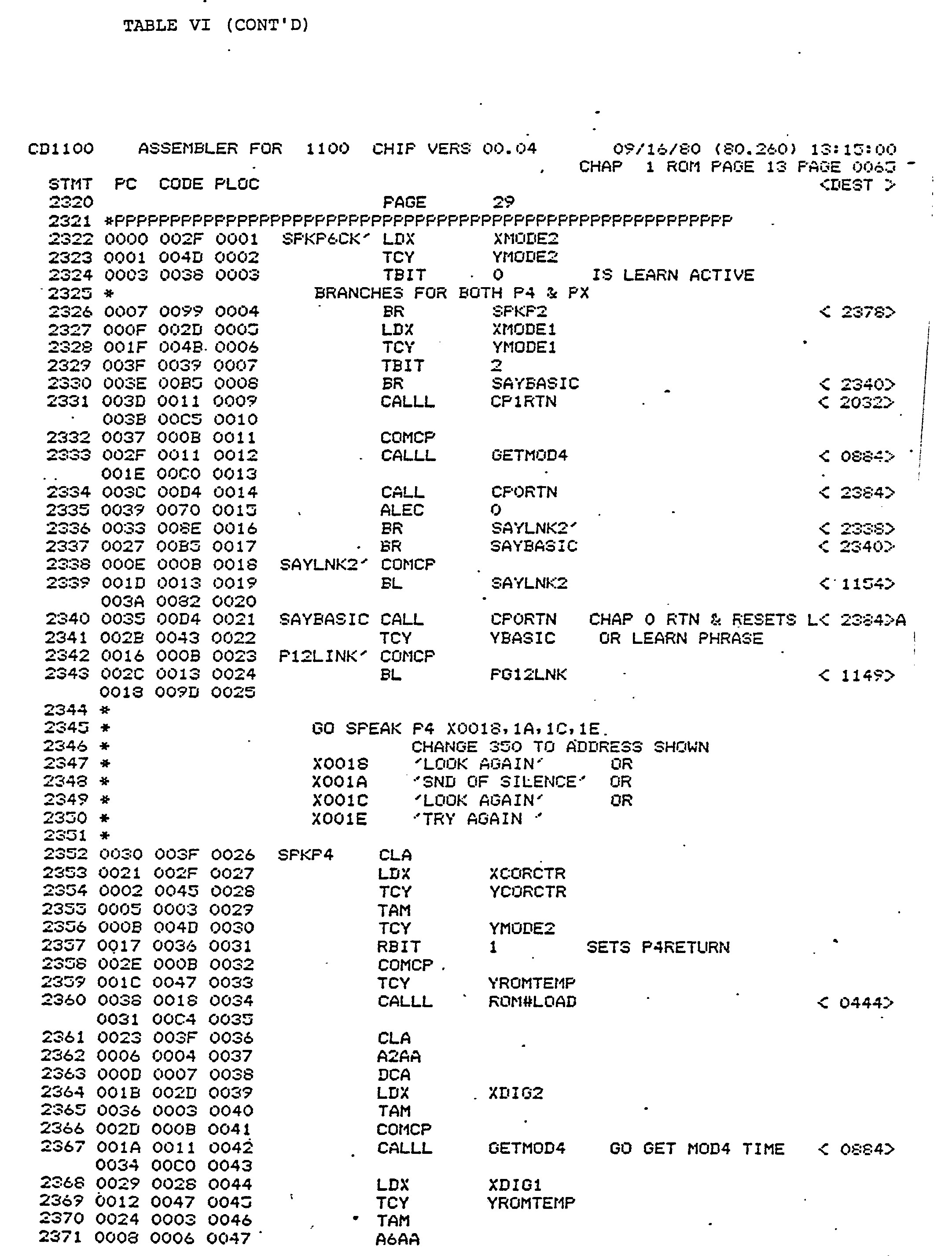


Claims (27)
Applications Claiming Priority (2)
| Application Number | Priority Date | Filing Date | Title |
|---|---|---|---|
| US192978 | 1980-10-01 | ||
| US06/192,978 US4403965A (en) | 1980-10-01 | 1980-10-01 | Electronic teaching apparatus |
Publications (3)
| Publication Number | Publication Date |
|---|---|
| EP0048835A2 true EP0048835A2 (en) | 1982-04-07 |
| EP0048835A3 EP0048835A3 (en) | 1983-06-08 |
| EP0048835B1 EP0048835B1 (en) | 1987-04-01 |
Family
ID=22711808
Family Applications (1)
| Application Number | Title | Priority Date | Filing Date |
|---|---|---|---|
| EP81106849A Expired EP0048835B1 (en) | 1980-10-01 | 1981-09-02 | Electronic teaching apparatus |
Country Status (5)
| Country | Link |
|---|---|
| US (1) | US4403965A (en) |
| EP (1) | EP0048835B1 (en) |
| JP (1) | JPS57122500A (en) |
| DE (1) | DE3176072D1 (en) |
| HK (1) | HK54288A (en) |
Cited By (4)
| Publication number | Priority date | Publication date | Assignee | Title |
|---|---|---|---|---|
| FR2598246A1 (en) * | 1986-05-05 | 1987-11-06 | Bertuzzi Nino | Mobile, manual device for producing sound by reading information recorded on magnetic panels |
| WO1990015402A1 (en) * | 1989-06-09 | 1990-12-13 | Telstar Enterprises Limited | A toy or educational device |
| EP0529596A1 (en) * | 1991-08-30 | 1993-03-03 | Sony Corporation | Auditory playing device |
| US5466158A (en) * | 1994-02-14 | 1995-11-14 | Smith, Iii; Jay | Interactive book device |
Families Citing this family (38)
| Publication number | Priority date | Publication date | Assignee | Title |
|---|---|---|---|---|
| JPS59116848A (en) * | 1982-12-23 | 1984-07-05 | Sharp Corp | Voice output system of electronic equipment |
| US4639877A (en) * | 1983-02-24 | 1987-01-27 | Jostens Learning Systems, Inc. | Phrase-programmable digital speech system |
| US4675840A (en) * | 1983-02-24 | 1987-06-23 | Jostens Learning Systems, Inc. | Speech processor system with auxiliary memory access |
| JPS59189663U (en) * | 1983-06-03 | 1984-12-15 | 三菱電機株式会社 | character learning machine |
| JPS6084572A (en) * | 1983-10-17 | 1985-05-13 | ソニー株式会社 | Talking card |
| US4829431A (en) * | 1983-12-27 | 1989-05-09 | Texas Instruments Incorporated | Method and apparatus for correlating test information |
| JPS63132323A (en) * | 1986-08-27 | 1988-06-04 | テキサス インスツルメンツ インコ−ポレイテツド | Data entry apparatus and interactive type communication |
| US5174759A (en) * | 1988-08-04 | 1992-12-29 | Preston Frank S | TV animation interactively controlled by the viewer through input above a book page |
| US4961579A (en) * | 1989-01-23 | 1990-10-09 | Tutor Toys, Inc. | Electronic puzzle game |
| US5010495A (en) * | 1989-02-02 | 1991-04-23 | American Language Academy | Interactive language learning system |
| CA2008423A1 (en) | 1989-02-10 | 1990-08-10 | Steven Lee Ruzic | Position-sensitive educational product |
| US4959017A (en) * | 1989-02-15 | 1990-09-25 | Tutor Toys, Inc. | Electronic learning device for teaching how to handle money |
| US5209665A (en) * | 1989-10-12 | 1993-05-11 | Sight & Sound Incorporated | Interactive audio visual work |
| US5087043A (en) * | 1990-02-09 | 1992-02-11 | Sight And Sound Inc. | Interactive audio-visual puzzle |
| US5188533B1 (en) * | 1990-06-01 | 1997-09-09 | Leapfrog Rbt Llc | Speech synthesizing indicia for interactive learning |
| US5177800A (en) * | 1990-06-07 | 1993-01-05 | Aisi, Inc. | Bar code activated speech synthesizer teaching device |
| KR100196757B1 (en) * | 1990-06-12 | 1999-06-15 | 다카노 야스아키 | Audio device with control function using a card |
| US5178545A (en) * | 1991-02-08 | 1993-01-12 | Tutor Toys, Inc. | Electronic puzzle game with unknown random time of play |
| GB9103768D0 (en) * | 1991-02-22 | 1991-04-10 | King Reginald A | Educational apparatus |
| US5813861A (en) * | 1994-02-23 | 1998-09-29 | Knowledge Kids Enterprises, Inc. | Talking phonics interactive learning device |
| US5569868A (en) * | 1994-08-24 | 1996-10-29 | Tiger Electronics, Inc. | Sound generating book |
| US5636995A (en) * | 1995-01-17 | 1997-06-10 | Stephen A. Schwartz | Interactive story book and graphics tablet apparatus and methods for operating the same |
| CA2216120A1 (en) * | 1995-02-07 | 1996-08-15 | Golden Books Publishing Company, Inc. | Electronic board game having clue delivery circuitry |
| US5803748A (en) | 1996-09-30 | 1998-09-08 | Publications International, Ltd. | Apparatus for producing audible sounds in response to visual indicia |
| US20030216944A1 (en) * | 2002-05-16 | 2003-11-20 | Robert Stavis | Communication system, especially for medical applications |
| TWI277021B (en) * | 2002-05-30 | 2007-03-21 | Mattel Inc | Interactive multi-sensory reading system electronic teaching/learning device |
| US7402042B2 (en) * | 2002-05-30 | 2008-07-22 | Mattel, Inc. | Electronic learning device for an interactive multi-sensory reading system |
| AU2003231952A1 (en) * | 2002-05-31 | 2003-12-19 | Mattel, Inc. | Book/clipped container combination |
| US20040213140A1 (en) * | 2003-01-31 | 2004-10-28 | Taylor John W. | Interactive electronic device with optical page identification system |
| WO2005038749A2 (en) * | 2003-10-10 | 2005-04-28 | Leapfrog Enterprises, Inc. | Display apparatus for teaching writing |
| US20050130111A1 (en) * | 2003-11-24 | 2005-06-16 | Otis Alton B.Jr. | Electronic educational game |
| US6893317B1 (en) | 2003-12-19 | 2005-05-17 | James Vlodek | Storybook lantern |
| US20050170324A1 (en) * | 2004-02-03 | 2005-08-04 | Sun Yu | Invisible ink quiz game |
| BRPI0400095B1 (en) * | 2004-03-31 | 2015-06-30 | Positivo Informática S A | Educational and recreational system for general language learning |
| US7659836B2 (en) * | 2005-07-20 | 2010-02-09 | Astrazeneca Ab | Device for communicating with a voice-disabled person |
| GB2434481A (en) * | 2006-01-21 | 2007-07-25 | Peter James Sexton | Electronic teaching machine for matching cards, e.g. words and pictures. |
| WO2011107888A1 (en) | 2010-02-25 | 2011-09-09 | Leigh Angus | Board game apparatus |
| USD1001906S1 (en) * | 2023-03-16 | 2023-10-17 | Danchun Lu | Early education machine |
Citations (5)
| Publication number | Priority date | Publication date | Assignee | Title |
|---|---|---|---|---|
| US3704337A (en) * | 1969-04-07 | 1972-11-28 | Information Transfer Corp | Tactile response teaching system |
| GB1308426A (en) * | 1971-06-08 | 1973-02-21 | Epoch Co Ltd | Educational device |
| DE2917161A1 (en) * | 1978-04-28 | 1979-11-29 | Texas Instruments Inc | ELECTRONIC LEARNING AIDS |
| US4189779A (en) * | 1978-04-28 | 1980-02-19 | Texas Instruments Incorporated | Parameter interpolator for speech synthesis circuit |
| US4215240A (en) * | 1977-11-11 | 1980-07-29 | Federal Screw Works | Portable voice system for the verbally handicapped |
Family Cites Families (10)
| Publication number | Priority date | Publication date | Assignee | Title |
|---|---|---|---|---|
| GB1286822A (en) * | 1968-08-14 | 1972-08-23 | Behavioural Res And Dev Ltd | Improvements in touch detecting teaching machines |
| US3579857A (en) * | 1969-10-03 | 1971-05-25 | Jack L Lamberson | Electric teaching device |
| GB1286823A (en) * | 1969-11-13 | 1972-08-23 | Behavioural Res And Dev Ltd | A touch detecting teaching machine |
| US3952426A (en) * | 1970-03-31 | 1976-04-27 | Walter Hesener | Question and answer educational game with an answer control device |
| US3760360A (en) * | 1971-11-01 | 1973-09-18 | E Systems Inc | Matrix switch |
| US3795989A (en) * | 1973-02-21 | 1974-03-12 | L Greenberg | Education apparatus |
| US3939579A (en) * | 1973-12-28 | 1976-02-24 | International Business Machines Corporation | Interactive audio-visual instruction device |
| US4030094A (en) * | 1975-07-14 | 1977-06-14 | Varian Associates | Device for selecting computer operational mode and labeling input controls accordingly |
| GB1546272A (en) * | 1977-03-25 | 1979-05-23 | Lim Boon Chen | Toys |
| JPS5655998A (en) * | 1979-10-15 | 1981-05-16 | Hitachi Ltd | Learning device using sound synthesizer |
-
1980
- 1980-10-01 US US06/192,978 patent/US4403965A/en not_active Expired - Lifetime
-
1981
- 1981-09-02 EP EP81106849A patent/EP0048835B1/en not_active Expired
- 1981-09-02 DE DE8181106849T patent/DE3176072D1/en not_active Expired
- 1981-10-01 JP JP56156927A patent/JPS57122500A/en active Pending
-
1988
- 1988-07-21 HK HK542/88A patent/HK54288A/en not_active IP Right Cessation
Patent Citations (5)
| Publication number | Priority date | Publication date | Assignee | Title |
|---|---|---|---|---|
| US3704337A (en) * | 1969-04-07 | 1972-11-28 | Information Transfer Corp | Tactile response teaching system |
| GB1308426A (en) * | 1971-06-08 | 1973-02-21 | Epoch Co Ltd | Educational device |
| US4215240A (en) * | 1977-11-11 | 1980-07-29 | Federal Screw Works | Portable voice system for the verbally handicapped |
| DE2917161A1 (en) * | 1978-04-28 | 1979-11-29 | Texas Instruments Inc | ELECTRONIC LEARNING AIDS |
| US4189779A (en) * | 1978-04-28 | 1980-02-19 | Texas Instruments Incorporated | Parameter interpolator for speech synthesis circuit |
Cited By (5)
| Publication number | Priority date | Publication date | Assignee | Title |
|---|---|---|---|---|
| FR2598246A1 (en) * | 1986-05-05 | 1987-11-06 | Bertuzzi Nino | Mobile, manual device for producing sound by reading information recorded on magnetic panels |
| WO1990015402A1 (en) * | 1989-06-09 | 1990-12-13 | Telstar Enterprises Limited | A toy or educational device |
| EP0529596A1 (en) * | 1991-08-30 | 1993-03-03 | Sony Corporation | Auditory playing device |
| US5334022A (en) * | 1991-08-30 | 1994-08-02 | Sony Corporation | Auditory playing device |
| US5466158A (en) * | 1994-02-14 | 1995-11-14 | Smith, Iii; Jay | Interactive book device |
Also Published As
| Publication number | Publication date |
|---|---|
| EP0048835A3 (en) | 1983-06-08 |
| DE3176072D1 (en) | 1987-05-07 |
| JPS57122500A (en) | 1982-07-30 |
| EP0048835B1 (en) | 1987-04-01 |
| US4403965A (en) | 1983-09-13 |
| HK54288A (en) | 1988-07-29 |
Similar Documents
| Publication | Publication Date | Title |
|---|---|---|
| EP0048835A2 (en) | Electronic teaching apparatus | |
| US4516260A (en) | Electronic learning aid or game having synthesized speech | |
| US4189779A (en) | Parameter interpolator for speech synthesis circuit | |
| US4304964A (en) | Variable frame length data converter for a speech synthesis circuit | |
| US4479124A (en) | Synthesized voice radio paging system | |
| US4209836A (en) | Speech synthesis integrated circuit device | |
| US4946391A (en) | Electronic arithmetic learning aid with synthetic speech | |
| JPH1083277A (en) | Connected read-aloud system and method for converting text into voice | |
| US4631748A (en) | Electronic handheld translator having miniature electronic speech synthesis chip | |
| US4441201A (en) | Speech synthesis system utilizing variable frame rate | |
| Lindblom | Models of phonetic variation and selection | |
| GB2077018A (en) | A talking electronic apparatus | |
| US4357489A (en) | Low voltage speech synthesis system with pulse width digital-to-analog converter | |
| US4331836A (en) | Speech synthesis integrated circuit device | |
| US4335275A (en) | Synchronous method and apparatus for speech synthesis circuit | |
| EP0033510A2 (en) | Speech synthesis system and method for exciting speech synthesis filter thereof | |
| US4970659A (en) | Learning aid or game having miniature electronic speech synthesis chip | |
| US4209781A (en) | MOS Digital-to-analog converter employing scaled field effect devices | |
| EP0036559A1 (en) | Electronic reading learning aid | |
| US4449233A (en) | Speech synthesis system with parameter look up table | |
| Frantz et al. | Design case history: Speak & Spell learns to talk | |
| US5027409A (en) | Apparatus for electronically outputting a voice and method for outputting a voice | |
| EP0042488A2 (en) | Electronic arithmetic learning aid | |
| Lerner | Computers: Products that talk: Speech-synthesis devices are being incorporated into dozens of products as difficult technical problems are solved | |
| US4468805A (en) | Variable frame length data converter for a speech synthesis circuit |
Legal Events
| Date | Code | Title | Description |
|---|---|---|---|
| PUAI | Public reference made under article 153(3) epc to a published international application that has entered the european phase |
Free format text: ORIGINAL CODE: 0009012 |
|
| AK | Designated contracting states |
Designated state(s): DE FR GB IT |
|
| PUAL | Search report despatched |
Free format text: ORIGINAL CODE: 0009013 |
|
| AK | Designated contracting states |
Designated state(s): DE FR GB IT |
|
| 17P | Request for examination filed |
Effective date: 19831124 |
|
| ITF | It: translation for a ep patent filed |
Owner name: BARZANO' E ZANARDO ROMA S.P.A. |
|
| GRAA | (expected) grant |
Free format text: ORIGINAL CODE: 0009210 |
|
| AK | Designated contracting states |
Kind code of ref document: B1 Designated state(s): DE FR GB IT |
|
| REF | Corresponds to: |
Ref document number: 3176072 Country of ref document: DE Date of ref document: 19870507 |
|
| ET | Fr: translation filed | ||
| PLBE | No opposition filed within time limit |
Free format text: ORIGINAL CODE: 0009261 |
|
| STAA | Information on the status of an ep patent application or granted ep patent |
Free format text: STATUS: NO OPPOSITION FILED WITHIN TIME LIMIT |
|
| 26N | No opposition filed | ||
| ITTA | It: last paid annual fee | ||
| PGFP | Annual fee paid to national office [announced via postgrant information from national office to epo] |
Ref country code: GB Payment date: 20000830 Year of fee payment: 20 |
|
| PGFP | Annual fee paid to national office [announced via postgrant information from national office to epo] |
Ref country code: FR Payment date: 20000922 Year of fee payment: 20 |
|
| PGFP | Annual fee paid to national office [announced via postgrant information from national office to epo] |
Ref country code: DE Payment date: 20001128 Year of fee payment: 20 |
|
| PG25 | Lapsed in a contracting state [announced via postgrant information from national office to epo] |
Ref country code: GB Free format text: LAPSE BECAUSE OF EXPIRATION OF PROTECTION Effective date: 20010901 |
|
| REG | Reference to a national code |
Ref country code: GB Ref legal event code: PE20 Effective date: 20010901 |