EP0044742B1 - Capacitor element - Google Patents
Capacitor element Download PDFInfo
- Publication number
- EP0044742B1 EP0044742B1 EP81303331A EP81303331A EP0044742B1 EP 0044742 B1 EP0044742 B1 EP 0044742B1 EP 81303331 A EP81303331 A EP 81303331A EP 81303331 A EP81303331 A EP 81303331A EP 0044742 B1 EP0044742 B1 EP 0044742B1
- Authority
- EP
- European Patent Office
- Prior art keywords
- capacitor
- electrode
- points
- wire
- capacitor element
- Prior art date
- Legal status (The legal status is an assumption and is not a legal conclusion. Google has not performed a legal analysis and makes no representation as to the accuracy of the status listed.)
- Expired
Links
Images




Classifications
-
- H—ELECTRICITY
- H01—ELECTRIC ELEMENTS
- H01G—CAPACITORS; CAPACITORS, RECTIFIERS, DETECTORS, SWITCHING DEVICES, LIGHT-SENSITIVE OR TEMPERATURE-SENSITIVE DEVICES OF THE ELECTROLYTIC TYPE
- H01G2/00—Details of capacitors not covered by a single one of groups H01G4/00-H01G11/00
-
- H—ELECTRICITY
- H01—ELECTRIC ELEMENTS
- H01G—CAPACITORS; CAPACITORS, RECTIFIERS, DETECTORS, SWITCHING DEVICES, LIGHT-SENSITIVE OR TEMPERATURE-SENSITIVE DEVICES OF THE ELECTROLYTIC TYPE
- H01G4/00—Fixed capacitors; Processes of their manufacture
- H01G4/002—Details
- H01G4/018—Dielectrics
- H01G4/06—Solid dielectrics
Definitions
- This invention relates to a capacitor element, and more particularly to a capacitor having parallel plates with a side length of more than about one fourth of a wavelength of a signal used in a microwave integrated circuit.
- distributed element circuits In conventional microwave circuits, distributed element circuits or lumped element circuits may be used.
- parameters such as resistance, inductance and capacitance are distributed as in a transmission line where the capacitance exists between the conductors, and the resistance and inductance are due to the conductors themselves.
- these parameters are lumped as used in a gate or source circuit of a GaAs FET, in which, the capacitance exists between a conductor and the ground, and these parameters can be treated for circuit analysis as a single inductance, capacitance, resistance, etc., when the frequency is sufficiently low.
- the lumped element circuit when used in such a high frequency, behaves as a distributed element circuit, and, accordingly, the designed values of the parameters become different from the practical values, as will be explained hereinafter in detail.
- an object of the present invention is to provide a capacitor element, the reactance of which does not change to an extremely large inductive reactance even when the used frequency becomes so high that the size of the electrode of the capacitor element reaches or exceeds about one quarter of the wavelength.
- Another object of the present invention is to provide a capacitor element which can be used in a lumped element circuit of a microwave circuit without deterioration of the characteristic of the lumped element circuit.
- a capacitor element according to the invention for microwave signals comprises a dielectric layer having two main surfaces, an electrode on one of the main surfaces and a conductive layer on the other main surface, and including at least one conductive wire joining two points on the said electrode; characterised in that the electrode extends continuously and in a straight line between the two points joined by the wire, the wire being spaced from the electrode between the said two points and having a length less than ⁇ 0/2 ⁇ r , where ⁇ o is the minimum wavelength for received signals and e r is the dielectric constant of the dielectric layer, whereby the tendency of the microwave capacitor to act as a transmission line is reduced.
- Fig. 1 is a conventional circuit diagram illustrating a lumped element circuit.
- two strip lines TL 1 and TL 2 are connected by inductances 1 1 and 1 2 .
- One electrode of a capacitor C is connected at a connecting point between the inductances 1 1 and 1 2 .
- the other electrode is grounded.
- the lumped constant circuit of Fig. 1 constitute a low-pass filter used in a microwave circuit.
- the circuit of Fig. 1 is constructed as shown in Fig. 2, which is a general perspective view illustrating the structure of the circuit of Fig. 1.
- the capacitor C is constructed by an electrode plate 10, a conduction substrate 14 made of copper and connected to the ground, and a dielectric film 12 between the electrode plate 10 and the conduction substrate 14.
- the inductances 1 1 and 1 2 are constituted by lead wires 16 and 18 which are connected between the electrode plate 10 and the strip lines TL, and TL 2 , respectively.
- the reactance of the circuit When a conventional capacitor is used in a lumped element circuit of a microwave integrated circuit, the reactance of the circuit often tends to be different from that of the designed value.
- One of the reasons why the reactance is changed is that, when the wave length of the electric signal applied to the lumped element circuit is decreased to less than 41, where I represents the side length of the electrode plate of the capacitor, the electrode plate acts as an inductance, or a transmission line, and does not act as the electrode of the capacitor.
- a transistor of this type is used in such a manner that a positive voltage is applied to its drain; its source is grounded; and a negative voltage is applied to its gate.
- two power supplies are required. Therefore, the source is grounded through a parallel circuit comprising a resistor and a capacitor so as to form a so-called self-biased circuit in which the negative voltage is not required to be applied to the gate so that the transistor can be operated by a single power supply.
- the capacitor has as its function to ground the source by conducting alternating currents.
- inductances of lead wires connected to the capacitor can not be neglected. Accordingly, the positioning of the capacitors becomes an important problem.
- Fig. 3A is a partial plan view illustrating the structure of a high power self-biased GaAs FET which was disclosed in EP-A-0015709, published on September 1980, after the priority date of the present patent.
- Fig. 3B is a cross-sectional view taken along line III-III' of Fig. 3A.
- capacitors are arranged close to the transistor. That is, in these figures, 20 represents a semiconductor chip on which a GaAs FET is formed; 22 and 32 represent the electrode plates of the capacitors; and 24 represents a grounded conduction substrate made of copper. On the conduction substrate 24, the semiconductor chip 20 is formed. Also on the conduction substrate 24, a dielectric film 23 is formed.
- the electrode plates 22 and 32 are formed on the dielectric film 23, the electrode plates 22 and 32 are formed.
- a package lead wire 26 for the gate and a package lead wire 28 for the drain are formed on the conduction substrate 24 through an insulating film 25; 30 represents a package lead wire for the source.
- These lead wires are connected to the gate electrode Eg, the drain electrode Ed, and the source electrode Es of the semiconductor chip 20 by wire bonding as illustrated.
- the gate electrode and the drain electrode have interdigitated structures as illustrated for the purpose of lowering the resistances of the electrodes and thus obtaining high power.
- the electrode plates 32 form capacitors for input impedance matching.
- the dielectric film 23 is made of, for example, barium titanate having a dielectric constant equal to about 140.
- the thickness of the dielectric film 23 is about 0.15 mm.
- the electrode plate 22, 32 over the dielectric film 23 or an electrode plate under the dielectric film 23 is formed by a titanium film having a thickness of about 1 pm covering the dielectric film 23, a palladium film having a thickness of about 1 11m covering the titanium film, and a gold film having a thickness of about 4 pm covering over palladium film.
- the capacitors are mounted on the conduction substrate by adhesive of, for example, gold-silicon alloy.
- Fig. 4 is an equivalent circuit diagram of the GaAs FET of Fig. 3A.
- the gate electrode of the transistor is connected through inductances 1 3 and 1 4 to the package lead 26.
- One electrode of a capacitor C 2 for input impedance matching is connected at a connecting point between the inductances 1 3 and 1 4 .
- the other electrode of the capacitor C 2 is grounded.
- the capacitor C 2 is formed by the electrode plates 32, the dielectric film 23 and the conduction substrate 24 in Figs. 3A and 3B.
- a capacitor C, for grounding high frequency components, or self biasing, is connected between the source electrode of the transistor and the ground.
- the capacitor C 1 is formed by the electrode plate 22, the dielectric film 23 and the conduction substrate in Figs. 3A and 3B.
- a resistor R for self biasing is connected to the capacitor C 1 in parallel.
- the resistor R is formed outside of the source package lead 30 in Fig. 3A.
- Fig. 5A is a plan view illustrating the capacitor C 1 for self biasing used in the device of Fig. 3A.
- Fig. 5B is a a cross-sectional view taken along line V-V' of Fig. 5A.
- the electrode plate 22 formed on the dielectric film 23 is electrically connected by a wire 1 5 to a measuring lead or a strip line 38 which is formed on another insulating film 34.
- the insulating film 34 is made of alumina (AI 2 0 3 ) having a thickness of about 0.65 mm.
- the strip line 38 is made of metal of, for example nichrome-gold series.
- the electrode plate 22 has recesses. Each recess has a depth d of 0.4 mm and a width w of 0.3 mm. The width w of the recess is equal to the width of the portion between each recess.
- Fig. 6 is an equivalent circuit diagram of the capacitor of Fig. 5.
- the capacity of the capacitor C, at a sufficiently low frequency is about 17.5 pF.
- the inductance of the wire 1 5 is about 0.3 nH. Therefore, the reactance X due to the capacitor C 1 and the wire 1 5 may be calculated as: where, w represents an angular frequency.
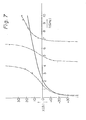
- the relation between the frequency and the reactance obtained from the above calculation is shown in Fig. 7 by a solid curve, in which, the reactance is capacitive when the frequency f is below 2.25 GH z and the reactance is inductive when the frequency f is above 2.25 GHz.
- the practical reactance X due to the capacitor C 1 and the wire 1 5 is different from the calculated reactance.
- the relation between the practical reactance and the frequency is illustrated in Fig. 7 by dashdot curves. This difference is caused mainly because, when the frequency is sufficiently high, the electrode plate 22 acts as a transmission line and does not act as the electrode of the capacitor C 1 as previously mentioned. More strictly, assume that the length of the capacitor C 1 is 2a+b as shown in Fig. 5A, the wavelength of the input signal applied to the gate of the transistor is ⁇ 0 , and the dielectric constant is ⁇ r . Then, the wavelength ⁇ of the input signal in the insulating film 23 is equal to ⁇ 0 / ⁇ r .
- Fig. 8 is a Smith chart of the equivalent circuit of Fig. 7.
- the reactance is negatively infinite as illustrated at a point So, i.e., the electrode plate 22 of the capacitor C 1 (Fig. 5) provides an open-circuit impedance.
- the reactance is capacitive, i.e., the inductance due to the electrode plate 22 can be neglected.
- the reactance When the frequency is increased so that the value ⁇ /4 is equal to 2a+b, the reactance is substantially equal to zero as illustrated at a point S 1 , i.e., the electrode plate 22 of the capacitance C 1 provides a short-circuit impedance.
- the reactance becomes inductive.
- the reactance is positively infinite as illustrated at the point So, i.e., the electrode plate 22 again provides an open-circuit impedance. Accordingly, as illustrated in Fig. 7 by dash-dot curves, practical reactances repeatedly vary from negative infinite to positive infinite. This problem will be further described as follows by using practical values.
- the dielectric constant ⁇ r is about 140.
- the transistor will cause an oscillation because currents cannot flow from the drain to the source but flow back to the gate, that is, feed-back becomes greater.
- the present invention provides a capacitor in which the reactance does not change to an extremely large inductive reactance. Now, an embodiment of the present invention will be described with reference to Figs. 9 and 10.
- Fig. 9 is a plan view illustrating a capacitor and a measuring lead 38 which corresponds to the conventional capacitor illustrated in Fig. 5.
- the difference between Fig. 5 and Fig. 9 is that, in Fig. 9, conduction wires L 1 , L 2 , L 3 , L 4 and L 5 are connected on the electrode plate 22 by wire bonding at points P 1 through P io .
- Each of the conduction wires L 1 through L 5 between the points P 1 and P 2 , P 3 and P 4 , P 5 and P 6 , P 7 and P 8 , and P a and Pg, respectively, is made of a gold wire having a diameter of 25 ⁇ m and has a dielectric constant ⁇ r substantially equal to 1, because the middle portion of each of the conduction wires L, through L 5 is separated from the electrode plate 22.
- the length of each of the conduction wires L 1 through L 5 is less than ⁇ 0 /2 ⁇ r , where ⁇ 0 represents the minimum wavelength of electric signals applied to the electrode plate 22 of the capacitor, and e, represents the dielectric constant of the insulating film 24.
- the capacitor according to this embodiment does not provide such an infinite inductive impedance as in the conventional capacitor C 1 , even when the frequency of an electric signal applied to the electrode plate 22 is high, so that the length 2a+b of the electrode plate 22 becomes larger than ⁇ 0 /4 ⁇ r . It is preferable that the length of each of the conduction wires L 1 through L 5 is less than ⁇ 0 /4 ⁇ r . Under this condition, the capacitor acts as a capacitor itself and does not show a characteristic like a transmission line.
- each of the conduction wires is less than ⁇ 0 /4.
- the conduction wires in Figure 9 do not overlap each other.
- Fig. 10 is a graph illustrating an experimental relation between the frequency and the reactance of the capacitor of Fig. 9, in comparison with the designed relation.
- the designed relation is again illustrated by a solid curve.
- the dotted curve represents the experimental relation.
- the experimental relation is quite similar to the designed relation for that capacitor.
- the capacitor can be used at a higher frequency than was possible in the prior art and thus, a capacitor useful for microwave transistor circuits can be obtained.
- the present invention is not restricted to the illustrated embodiment, but may be applied to any capacitor for use at high frequencies.
Landscapes
- Engineering & Computer Science (AREA)
- Power Engineering (AREA)
- Microelectronics & Electronic Packaging (AREA)
- Manufacturing & Machinery (AREA)
- Microwave Amplifiers (AREA)
- Waveguide Connection Structure (AREA)
- Waveguides (AREA)
- Semiconductor Integrated Circuits (AREA)
Description
- This invention relates to a capacitor element, and more particularly to a capacitor having parallel plates with a side length of more than about one fourth of a wavelength of a signal used in a microwave integrated circuit.
- In conventional microwave circuits, distributed element circuits or lumped element circuits may be used. In a distributed element circuit, parameters such as resistance, inductance and capacitance are distributed as in a transmission line where the capacitance exists between the conductors, and the resistance and inductance are due to the conductors themselves. In contrast, in a lumped element circuit, these parameters are lumped as used in a gate or source circuit of a GaAs FET, in which, the capacitance exists between a conductor and the ground, and these parameters can be treated for circuit analysis as a single inductance, capacitance, resistance, etc., when the frequency is sufficiently low. However, when the frequency used in a lumped element circuit is very high, especially when the size of the electrode of the capacitor reaches or exceeds about one quarter of the wavelength, we have to consider the effect of size on reactance, that is to say, the change of reactance of the capacitor from capacitive reactance to inductive reactance. Therefore, the lumped element circuit, when used in such a high frequency, behaves as a distributed element circuit, and, accordingly, the designed values of the parameters become different from the practical values, as will be explained hereinafter in detail.
- Accordingly, an object of the present invention is to provide a capacitor element, the reactance of which does not change to an extremely large inductive reactance even when the used frequency becomes so high that the size of the electrode of the capacitor element reaches or exceeds about one quarter of the wavelength.
- Another object of the present invention is to provide a capacitor element which can be used in a lumped element circuit of a microwave circuit without deterioration of the characteristic of the lumped element circuit.
- A capacitor element according to the invention for microwave signals comprises a dielectric layer having two main surfaces, an electrode on one of the main surfaces and a conductive layer on the other main surface, and including at least one conductive wire joining two points on the said electrode; characterised in that the electrode extends continuously and in a straight line between the two points joined by the wire, the wire being spaced from the electrode between the said two points and having a length less than λ0/2√εr, where λo is the minimum wavelength for received signals and er is the dielectric constant of the dielectric layer, whereby the tendency of the microwave capacitor to act as a transmission line is reduced.
- It has been proposed, in GB-A-1 469 944, that to reduce undesirable resonances in planar thin-film capacitors of the interdigitated kind, spaced fingers of the same electrode are bridged by a conductive link, the link extending over the intermediate finger of the other electrode.
- To enable the invention to be better understood, examples of prior circuit elements and an embodiment of the present invention will now be described with reference to the accompanying drawings, wherein:
- Fig. 1 is a circuit diagram illustrating a lumped element circuit for explaining the problem in a conventional capacitor;
- Fig. 2 is a general perspective view illustrating the structure of the circuit of Fig. 1 in an integrated circuit;
- Fig. 3A is a partial plan view illustrating the structure of a known high-power self-biased GaAs FET;
- Fig. 3B is a cross-sectional view taken along line III-III' of Fig. 3A;
- Fig. 4 is an equivalent circuit diagram of the GaAs FET of Fig. 3A;
- Fig. 5A is a plan view illustrating a capacitor used in the device of Fig. 3A and a measuring lead;
- Fig. 5B is a cross-sectional view taken along line V-V' of Fig. 5A;
- Fig. 6 is an equivalent circuit of the device of Fig. 5;
- Fig. 7 is a graph illustrating the designed relation and the practical relation between the frequency and the reactance of the capacitor of Fig. 5;
- Fig. 8 is a Smith chart for explaining the impedance of the capacitor of Fig. 5; and
- Fig. 9 is a plan view illustrating a capacitor according to an embodiment of the present invention.
- Fig. 10 is a graph illustrating the designed relation and the experimental relation between the frequency and the reactance of the capacitor of Fig. 9.
- Before explaining a preferred embodiment of the present invention, the problems in the conventional capacitor will first be explained with reference to Figs. 1 through 7.
- Fig. 1 is a conventional circuit diagram illustrating a lumped element circuit. In Fig. 1, two strip lines TL1 and TL2 are connected by
inductances inductances - In a microwave integrated circuit, the circuit of Fig. 1 is constructed as shown in Fig. 2, which is a general perspective view illustrating the structure of the circuit of Fig. 1. In Fig. 2, the capacitor C is constructed by an
electrode plate 10, aconduction substrate 14 made of copper and connected to the ground, and adielectric film 12 between theelectrode plate 10 and theconduction substrate 14. Theinductances lead wires electrode plate 10 and the strip lines TL, and TL2, respectively. - When a conventional capacitor is used in a lumped element circuit of a microwave integrated circuit, the reactance of the circuit often tends to be different from that of the designed value. One of the reasons why the reactance is changed is that, when the wave length of the electric signal applied to the lumped element circuit is decreased to less than 41, where I represents the side length of the electrode plate of the capacitor, the electrode plate acts as an inductance, or a transmission line, and does not act as the electrode of the capacitor.
- This reason will be explained in detail in conjunction with a known high power GaAs FET used in microwaves. A transistor of this type is used in such a manner that a positive voltage is applied to its drain; its source is grounded; and a negative voltage is applied to its gate. However, by this connection, two power supplies are required. Therefore, the source is grounded through a parallel circuit comprising a resistor and a capacitor so as to form a so-called self-biased circuit in which the negative voltage is not required to be applied to the gate so that the transistor can be operated by a single power supply. The capacitor has as its function to ground the source by conducting alternating currents. However, when the frequency of the signal applied to the transistor is extremely high, inductances of lead wires connected to the capacitor can not be neglected. Accordingly, the positioning of the capacitors becomes an important problem.
- Fig. 3A is a partial plan view illustrating the structure of a high power self-biased GaAs FET which was disclosed in EP-A-0015709, published on September 1980, after the priority date of the present patent. Fig. 3B is a cross-sectional view taken along line III-III' of Fig. 3A. Referring to Figs. 3A and 3B, capacitors are arranged close to the transistor. That is, in these figures, 20 represents a semiconductor chip on which a GaAs FET is formed; 22 and 32 represent the electrode plates of the capacitors; and 24 represents a grounded conduction substrate made of copper. On the
conduction substrate 24, thesemiconductor chip 20 is formed. Also on theconduction substrate 24, adielectric film 23 is formed. On thedielectric film 23, theelectrode plates package lead wire 26 for the gate and apackage lead wire 28 for the drain are formed on theconduction substrate 24 through aninsulating film 25; 30 represents a package lead wire for the source. These lead wires are connected to the gate electrode Eg, the drain electrode Ed, and the source electrode Es of thesemiconductor chip 20 by wire bonding as illustrated. The gate electrode and the drain electrode have interdigitated structures as illustrated for the purpose of lowering the resistances of the electrodes and thus obtaining high power. Theelectrode plates 32 form capacitors for input impedance matching. - The
dielectric film 23 is made of, for example, barium titanate having a dielectric constant equal to about 140. The thickness of thedielectric film 23 is about 0.15 mm. - The
electrode plate dielectric film 23 or an electrode plate under the dielectric film 23 (not shown) is formed by a titanium film having a thickness of about 1 pm covering thedielectric film 23, a palladium film having a thickness of about 1 11m covering the titanium film, and a gold film having a thickness of about 4 pm covering over palladium film. The capacitors are mounted on the conduction substrate by adhesive of, for example, gold-silicon alloy. - Fig. 4 is an equivalent circuit diagram of the GaAs FET of Fig. 3A. In Fig. 4, the gate electrode of the transistor is connected through
inductances package lead 26. One electrode of a capacitor C2 for input impedance matching is connected at a connecting point between theinductances electrode plates 32, thedielectric film 23 and theconduction substrate 24 in Figs. 3A and 3B. A capacitor C, for grounding high frequency components, or self biasing, is connected between the source electrode of the transistor and the ground. The capacitor C1 is formed by theelectrode plate 22, thedielectric film 23 and the conduction substrate in Figs. 3A and 3B. Also, a resistor R for self biasing is connected to the capacitor C1 in parallel. The resistor R is formed outside of thesource package lead 30 in Fig. 3A. - Because the size of the
electrode plate 22 of the capacitor C1 for self biasing is rather large, the previously mentioned problem is caused, as will be explained in more detail in conjunction with Figs. 5 through 8. - Fig. 5A is a plan view illustrating the capacitor C1 for self biasing used in the device of Fig. 3A. Fig. 5B is a a cross-sectional view taken along line V-V' of Fig. 5A. Referring to Figs. 5A and 5B, the
electrode plate 22 formed on thedielectric film 23 is electrically connected by awire 15 to a measuring lead or astrip line 38 which is formed on another insulatingfilm 34. The insulatingfilm 34 is made of alumina (AI203) having a thickness of about 0.65 mm. Thestrip line 38 is made of metal of, for example nichrome-gold series. As shown in Fig. 5A, theelectrode plate 22 has recesses. Each recess has a depth d of 0.4 mm and a width w of 0.3 mm. The width w of the recess is equal to the width of the portion between each recess. - Fig. 6 is an equivalent circuit diagram of the capacitor of Fig. 5. In Fig. 6, the capacity of the capacitor C, at a sufficiently low frequency is about 17.5 pF. The inductance of the
wire 15 is about 0.3 nH. Therefore, the reactance X due to the capacitor C1 and thewire 15 may be calculated as:
- However, the practical reactance X due to the capacitor C1 and the
wire 15 is different from the calculated reactance. The relation between the practical reactance and the frequency is illustrated in Fig. 7 by dashdot curves. This difference is caused mainly because, when the frequency is sufficiently high, theelectrode plate 22 acts as a transmission line and does not act as the electrode of the capacitor C1 as previously mentioned. More strictly, assume that the length of the capacitor C1 is 2a+b as shown in Fig. 5A, the wavelength of the input signal applied to the gate of the transistor is λ0, and the dielectric constant is εr. Then, the wavelength λ of the input signal in the insulatingfilm 23 is equal to λ0/√εr. When the frequency of the input signal becomes higher, the wavelength will then become shorter in comparison with the side length 2a+b of theelectrode plate 22 of the capacitor C1. This will be easily understood from Fig. 8 which is a Smith chart of the equivalent circuit of Fig. 7. Referring to Fig. 8, when the frequency is sufficiently low so that the value λ/4 is much larger than 2a+b, the reactance is negatively infinite as illustrated at a point So, i.e., theelectrode plate 22 of the capacitor C1 (Fig. 5) provides an open-circuit impedance. When the frequency is relatively low so that the value λ/4 is larger than 2a+b, the reactance is capacitive, i.e., the inductance due to theelectrode plate 22 can be neglected. When the frequency is increased so that the value λ/4 is equal to 2a+b, the reactance is substantially equal to zero as illustrated at a point S1, i.e., theelectrode plate 22 of the capacitance C1 provides a short-circuit impedance. When the frequency is more increased so that the value λ/4 is smaller than 2a+b, the reactance becomes inductive. When the frequency is further increased so that the value λ/2 is equal to 2a+b, the reactance is positively infinite as illustrated at the point So, i.e., theelectrode plate 22 again provides an open-circuit impedance. Accordingly, as illustrated in Fig. 7 by dash-dot curves, practical reactances repeatedly vary from negative infinite to positive infinite. This problem will be further described as follows by using practical values. - The length of the
electrode plate 22 is about 3 mm (a=0.75 mm, b=1.5 mm). The dielectric constant εr is about 140. When the measurement frequency f is 4GHz, the value λ0/2 is equal to about 36 mm, and accordingly, the value λ/2=λ0/2√εr is equal to about 3 mm which is the length of theelectrode plate 22. Therefore, if the wire I5 is bonded to theelectrode plate 22 as illustrated in Fig. 5, the capacitor C1 does not act as a capacitor but provides an open-circuit impedance. - Referring back to Fig. 4, if the source of the transistor has such an infinite inductive impedance, the transistor will cause an oscillation because currents cannot flow from the drain to the source but flow back to the gate, that is, feed-back becomes greater.
- The present invention provides a capacitor in which the reactance does not change to an extremely large inductive reactance. Now, an embodiment of the present invention will be described with reference to Figs. 9 and 10.
- Fig. 9 is a plan view illustrating a capacitor and a measuring
lead 38 which corresponds to the conventional capacitor illustrated in Fig. 5. The difference between Fig. 5 and Fig. 9 is that, in Fig. 9, conduction wires L1, L2, L3, L4 and L5 are connected on theelectrode plate 22 by wire bonding at points P1 through Pio. Each of the conduction wires L1 through L5 between the points P1 and P2, P3 and P4, P5 and P6, P7 and P8, and Pa and Pg, respectively, is made of a gold wire having a diameter of 25 µm and has a dielectric constant εr substantially equal to 1, because the middle portion of each of the conduction wires L, through L5 is separated from theelectrode plate 22. The length of each of the conduction wires L1 through L5 is less than λ0/2√εr, where λ0 represents the minimum wavelength of electric signals applied to theelectrode plate 22 of the capacitor, and e, represents the dielectric constant of the insulatingfilm 24. In this structure we can regard the wavelength along a wire as that in air. By this construction, because many points distributed over the entire surface of theelectrode plate 22 are short-circuited by the conduction wires, L1 through L5, each having a length less than λ0/2√εr, the capacitor according to this embodiment does not provide such an infinite inductive impedance as in the conventional capacitor C1, even when the frequency of an electric signal applied to theelectrode plate 22 is high, so that the length 2a+b of theelectrode plate 22 becomes larger than λ0/4√εr. It is preferable that the length of each of the conduction wires L1 through L5 is less than λ0/4√εr. Under this condition, the capacitor acts as a capacitor itself and does not show a characteristic like a transmission line. - Further, it is sufficient that the length of each of the conduction wires is less than λ0/4. The conduction wires in Figure 9 do not overlap each other.
- Fig. 10 is a graph illustrating an experimental relation between the frequency and the reactance of the capacitor of Fig. 9, in comparison with the designed relation. Referring to Fig. 10, the designed relation is again illustrated by a solid curve. The dotted curve represents the experimental relation. As will be apparent from Fig. 10, the experimental relation is quite similar to the designed relation for that capacitor.
- From the foregoing description, it will be apparent that, according. to the present invention, by means of a simple technique of forming short-circuits between the centre and a side or between sides of an electrode plate of a capacitor by wires, the middle portions of which are separated from the electrode plate, the capacitor can be used at a higher frequency than was possible in the prior art and thus, a capacitor useful for microwave transistor circuits can be obtained.
- The present invention is not restricted to the illustrated embodiment, but may be applied to any capacitor for use at high frequencies.
Claims (6)
Applications Claiming Priority (2)
| Application Number | Priority Date | Filing Date | Title |
|---|---|---|---|
| JP55099684A JPS6035843B2 (en) | 1980-07-21 | 1980-07-21 | capacitor |
| JP99684/80 | 1980-07-21 |
Publications (3)
| Publication Number | Publication Date |
|---|---|
| EP0044742A2 EP0044742A2 (en) | 1982-01-27 |
| EP0044742A3 EP0044742A3 (en) | 1984-10-10 |
| EP0044742B1 true EP0044742B1 (en) | 1987-11-25 |
Family
ID=14253858
Family Applications (1)
| Application Number | Title | Priority Date | Filing Date |
|---|---|---|---|
| EP81303331A Expired EP0044742B1 (en) | 1980-07-21 | 1981-07-21 | Capacitor element |
Country Status (4)
| Country | Link |
|---|---|
| US (1) | US4384215A (en) |
| EP (1) | EP0044742B1 (en) |
| JP (1) | JPS6035843B2 (en) |
| DE (1) | DE3176550D1 (en) |
Families Citing this family (4)
| Publication number | Priority date | Publication date | Assignee | Title |
|---|---|---|---|---|
| JPS6122656A (en) * | 1984-07-10 | 1986-01-31 | Nec Corp | Transistor element for oscillation |
| JPH04330801A (en) * | 1991-03-07 | 1992-11-18 | Fujitsu Ltd | Capacitor module for bias circuit of microwave integrated circuit and microwave module equipped with said capacitor module |
| US6887290B2 (en) * | 2002-09-25 | 2005-05-03 | Federal Signal Corporation | Debris separation and filtration systems |
| US10240884B1 (en) | 2013-03-14 | 2019-03-26 | The United States Of America As Represented By The Secretary Of The Navy | Mountable fixture for absorbing recoil |
Family Cites Families (4)
| Publication number | Priority date | Publication date | Assignee | Title |
|---|---|---|---|---|
| US1547242A (en) * | 1924-04-29 | 1925-07-28 | American Telephone & Telegraph | Carrier transmission over power circuits |
| US2195986A (en) * | 1936-01-11 | 1940-04-02 | Rca Corp | Transmission line transposition |
| US3465267A (en) * | 1966-03-04 | 1969-09-02 | Ernest H Carlson Jr | Circuit component |
| GB1469944A (en) * | 1975-04-21 | 1977-04-06 | Decca Ltd | Planar capacitor |
-
1980
- 1980-07-21 JP JP55099684A patent/JPS6035843B2/en not_active Expired
-
1981
- 1981-07-21 EP EP81303331A patent/EP0044742B1/en not_active Expired
- 1981-07-21 DE DE8181303331T patent/DE3176550D1/en not_active Expired
- 1981-07-21 US US06/285,472 patent/US4384215A/en not_active Expired - Fee Related
Also Published As
| Publication number | Publication date |
|---|---|
| JPS6035843B2 (en) | 1985-08-16 |
| EP0044742A3 (en) | 1984-10-10 |
| JPS5724101A (en) | 1982-02-08 |
| DE3176550D1 (en) | 1988-01-07 |
| EP0044742A2 (en) | 1982-01-27 |
| US4384215A (en) | 1983-05-17 |
Similar Documents
| Publication | Publication Date | Title |
|---|---|---|
| US4843440A (en) | Microwave field effect transistor | |
| US4617586A (en) | High-frequency circuit comprising an integrated capacitor | |
| EP0949754B1 (en) | High-frequency power amplifier circuit and high-frequency power amplifier module | |
| US4680557A (en) | Staggered ground-plane microstrip transmission line | |
| US5233310A (en) | Microwave integrated circuit | |
| US4479100A (en) | Impedance matching network comprising selectable capacitance pads and selectable inductance strips or pads | |
| EP0592002A2 (en) | Microwave integrated circuit | |
| US5233313A (en) | High power field effect transistor amplifier | |
| EP0015709B1 (en) | Constructional arrangement for semiconductor devices | |
| JPH0766949B2 (en) | IC package | |
| US3678433A (en) | Rf rejection filter | |
| EP2695191A1 (en) | Improved matching techniques for wide-bandgap power transistors | |
| US7034631B2 (en) | Symmetric microwave filter and microwave integrated circuit merging the same | |
| US4594557A (en) | Traveling wave video detector | |
| JPH07297609A (en) | Semiconductor device | |
| CA1090915A (en) | Surface acoustic wave apparatus | |
| JP3756129B2 (en) | Transmission line type noise filter | |
| US5670917A (en) | AC coupled termination | |
| CA2188962C (en) | High-frequency amplifier integrated circuit device | |
| CA1200017A (en) | Microwave field effect transistor | |
| EP0044742A2 (en) | Capacitor element | |
| JPH02284501A (en) | Surface mounting type strip line resonator | |
| US20040223306A1 (en) | AC coupling circuit having a large capacitance and a good frequency response | |
| JPH0416012A (en) | Noise filter | |
| US5986516A (en) | Chip attenuator having a capacitor therein |
Legal Events
| Date | Code | Title | Description |
|---|---|---|---|
| PUAI | Public reference made under article 153(3) epc to a published international application that has entered the european phase |
Free format text: ORIGINAL CODE: 0009012 |
|
| AK | Designated contracting states |
Designated state(s): DE FR GB IT NL SE |
|
| PUAL | Search report despatched |
Free format text: ORIGINAL CODE: 0009013 |
|
| AK | Designated contracting states |
Designated state(s): DE FR GB IT NL SE |
|
| 17P | Request for examination filed |
Effective date: 19841205 |
|
| 17Q | First examination report despatched |
Effective date: 19860813 |
|
| GRAA | (expected) grant |
Free format text: ORIGINAL CODE: 0009210 |
|
| AK | Designated contracting states |
Kind code of ref document: B1 Designated state(s): DE FR GB IT NL SE |
|
| PG25 | Lapsed in a contracting state [announced via postgrant information from national office to epo] |
Ref country code: NL Effective date: 19871125 |
|
| REF | Corresponds to: |
Ref document number: 3176550 Country of ref document: DE Date of ref document: 19880107 |
|
| ITF | It: translation for a ep patent filed | ||
| ET | Fr: translation filed | ||
| NLV1 | Nl: lapsed or annulled due to failure to fulfill the requirements of art. 29p and 29m of the patents act | ||
| PLBE | No opposition filed within time limit |
Free format text: ORIGINAL CODE: 0009261 |
|
| STAA | Information on the status of an ep patent application or granted ep patent |
Free format text: STATUS: NO OPPOSITION FILED WITHIN TIME LIMIT |
|
| 26N | No opposition filed | ||
| ITTA | It: last paid annual fee | ||
| PGFP | Annual fee paid to national office [announced via postgrant information from national office to epo] |
Ref country code: SE Payment date: 19930616 Year of fee payment: 13 |
|
| PGFP | Annual fee paid to national office [announced via postgrant information from national office to epo] |
Ref country code: GB Payment date: 19930712 Year of fee payment: 13 |
|
| PGFP | Annual fee paid to national office [announced via postgrant information from national office to epo] |
Ref country code: FR Payment date: 19930729 Year of fee payment: 13 |
|
| PGFP | Annual fee paid to national office [announced via postgrant information from national office to epo] |
Ref country code: DE Payment date: 19930917 Year of fee payment: 13 |
|
| PG25 | Lapsed in a contracting state [announced via postgrant information from national office to epo] |
Ref country code: GB Effective date: 19940721 |
|
| PG25 | Lapsed in a contracting state [announced via postgrant information from national office to epo] |
Ref country code: SE Effective date: 19940722 |
|
| EUG | Se: european patent has lapsed |
Ref document number: 81303331.3 Effective date: 19950210 |
|
| GBPC | Gb: european patent ceased through non-payment of renewal fee |
Effective date: 19940721 |
|
| PG25 | Lapsed in a contracting state [announced via postgrant information from national office to epo] |
Ref country code: FR Effective date: 19950331 |
|
| PG25 | Lapsed in a contracting state [announced via postgrant information from national office to epo] |
Ref country code: DE Effective date: 19950401 |
|
| EUG | Se: european patent has lapsed |
Ref document number: 81303331.3 |
|
| REG | Reference to a national code |
Ref country code: FR Ref legal event code: ST |