EP0044450B1 - Digital adder circuit - Google Patents
Digital adder circuit Download PDFInfo
- Publication number
- EP0044450B1 EP0044450B1 EP81105138A EP81105138A EP0044450B1 EP 0044450 B1 EP0044450 B1 EP 0044450B1 EP 81105138 A EP81105138 A EP 81105138A EP 81105138 A EP81105138 A EP 81105138A EP 0044450 B1 EP0044450 B1 EP 0044450B1
- Authority
- EP
- European Patent Office
- Prior art keywords
- operands
- multiplexers
- correction value
- carry
- circuit
- Prior art date
- Legal status (The legal status is an assumption and is not a legal conclusion. Google has not performed a legal analysis and makes no representation as to the accuracy of the status listed.)
- Expired
Links
Images


Classifications
-
- G—PHYSICS
- G06—COMPUTING OR CALCULATING; COUNTING
- G06F—ELECTRIC DIGITAL DATA PROCESSING
- G06F7/00—Methods or arrangements for processing data by operating upon the order or content of the data handled
- G06F7/38—Methods or arrangements for performing computations using exclusively denominational number representation, e.g. using binary, ternary, decimal representation
- G06F7/48—Methods or arrangements for performing computations using exclusively denominational number representation, e.g. using binary, ternary, decimal representation using non-contact-making devices, e.g. tube, solid state device; using unspecified devices
- G06F7/491—Computations with decimal numbers radix 12 or 20.
- G06F7/492—Computations with decimal numbers radix 12 or 20. using a binary weighted representation within each denomination
- G06F7/493—Computations with decimal numbers radix 12 or 20. using a binary weighted representation within each denomination the representation being the natural binary coded representation, i.e. 8421-code
- G06F7/494—Adding; Subtracting
-
- G—PHYSICS
- G06—COMPUTING OR CALCULATING; COUNTING
- G06F—ELECTRIC DIGITAL DATA PROCESSING
- G06F7/00—Methods or arrangements for processing data by operating upon the order or content of the data handled
- G06F7/38—Methods or arrangements for performing computations using exclusively denominational number representation, e.g. using binary, ternary, decimal representation
- G06F7/48—Methods or arrangements for performing computations using exclusively denominational number representation, e.g. using binary, ternary, decimal representation using non-contact-making devices, e.g. tube, solid state device; using unspecified devices
- G06F7/57—Arithmetic logic units [ALU], i.e. arrangements or devices for performing two or more of the operations covered by groups G06F7/483 – G06F7/556 or for performing logical operations
- G06F7/575—Basic arithmetic logic units, i.e. devices selectable to perform either addition, subtraction or one of several logical operations, using, at least partially, the same circuitry
-
- G—PHYSICS
- G06—COMPUTING OR CALCULATING; COUNTING
- G06F—ELECTRIC DIGITAL DATA PROCESSING
- G06F2207/00—Indexing scheme relating to methods or arrangements for processing data by operating upon the order or content of the data handled
- G06F2207/38—Indexing scheme relating to groups G06F7/38 - G06F7/575
- G06F2207/48—Indexing scheme relating to groups G06F7/48 - G06F7/575
- G06F2207/4802—Special implementations
- G06F2207/4812—Multiplexers
-
- G—PHYSICS
- G06—COMPUTING OR CALCULATING; COUNTING
- G06F—ELECTRIC DIGITAL DATA PROCESSING
- G06F2207/00—Indexing scheme relating to methods or arrangements for processing data by operating upon the order or content of the data handled
- G06F2207/492—Indexing scheme relating to groups G06F7/492 - G06F7/496
- G06F2207/4921—Single digit adding or subtracting
Definitions
- This invention relates to a digital adder circuit according to the precharacterising part of claim 1.
- Adder circuits are known which are capable of adding operands of radix other than a power of two e.g. decimal operands.
- U.S. Patent No. 4172288 describes a method of adding two binary decimal (BCD) operands by first adding the operands as if they were pure binary numbers to form an intermediate result, and then, if necessary, adding a correction value of six to the intermediate result to give the correct BCD result.
- the condition for adding the correction value is that the intermediate result is greater than or equal to ten.
- a problem with this is that a normal binary adder does not have any logic for detecting whether the sum is greater than or equal to ten. As a result, special logic must be provided to do this.
- U.S. Patent No. 3,958,112 describes an alternative arrangement in which the correction value of six is always added to one of the operands before the operands are added together and then, if necessary, the correction value is subtracted from the result.
- the condition for subtracting the correction value is that the result of the addition is less than sixteen, which is an easy condition to detect since it is simply the inverse of the normal binary adder overflow condition.
- the addition of the correction value before the addition of the operands introduces an extra stage which slows down the overall operation of the circuit.
- the object of the present invention is to avoid this reduction of operating speed.
- a digital adder circuit operable to form the sum of two n-bit operands representing binary-coded numbers whose radix is not limited to being an integer power of two, wherein a correction value equal to the difference between 2" and said radix is added to the operands and the operands are added together in a logic circuit to form an intermediate result, and wherein the correction value is subtracted from the intermediate result if the intermediate result is less than 2", characterised in that the logic circuit (10) includes a plurality of multiplexers (MX) controlled by the values of the operands (AO-A3, BO-B3) and conditioned by a pattern of input bits (PF, PFX, GF, GFX) which depends on the correction value so as to produce carry generate and propagate signals (GO - G 3 , P o P 3 ) corresponding to the addition of the correction value simultaneously with the addition of the operands.
- MX multiplexers
- multiplexers in this way is particularly advantageous, since it permits the addition the correction value with virtually no extra circuitry over and above that required to perform the addition of the two operands. Moreover, by conditioning the multiplexers with different patterns of bits, the circuit can be made to perform pure binary addition or various logic functions.
- the digital adder circuit receives two four-bit operands AO-A3, BO-B3 (where AO and BO are the most significant bits) and produces a four-bit sum output SUM.
- the circuit also receives a carry-in signal C.
- the circuit is designed to form one stage of a multi-stage adder with look-ahead carry between the stages. This means that, instead of providing a carry-out signal, it produces a carry propagate signal P and a carry generate signal G.
- the propagate signal P signifies that this stage propagates any carry-in applied to it, i.e. that the carry-in to the next stage should be equal to the carry-in C to this stage.
- the generate signal G indicates that this stage generates a carry i.e. that the carry-in to the next stage must be one, irrespective of the value of the carry in to this stage.
- the principles of look-ahead carry addition are well known (see for example an article by O. L. MacSorley entitled "High Speed Arithmetic in Binary Computers, Proceedings of the IRE, January 1961, Pages 67-91) and so will not be described in detail herein.
- the two operands AO-A3, B0B3 are applied to a binary adder 10, consisting of a group of multiplexers 11 and a look-ahead carry circuit 12.
- the look-ahead carry circuit 12 receives these signals and produces a four-bit intermediate result signal IR, and also produces the inter-stage propagate and generate signals P and G.
- the multiplexers 11 are controlled by a function control circuit 13 which is in turn controlled by a set of function control bits FN, and a decimal operation control signal DEC.
- the intermediate result signal IR is applied to an incrementer circuit 14 which increments it by one to produce a signal IR+1 which represents the value required for the intermediate result when the carry in C is one.
- the signal IR and IR+1 are applied to respective decimal adjustment circuits 15 and 16 each of which is selectively operable to subtract the decimal correction value of six.
- the circuits 15, 16 are respectively controlled by signals ADJ and ADJ' from a decimal adjustment control circuit 17.
- This circuit 17 is in turn controlled by the signal DEC and by the inter-stage propagate and generate signals P and G.
- the selected signal appears at the output of the multiplexer 18 as the final result SUM.
- the outputs of each pair represent the corresponding inter-bit generate and propagate signals Gi and Pi.
- each multiplexer MX has four data bit inputs 0-3, which are connected to receive a four-bit control signal PF, PFX, GF or GFX as shown. These signals are derived from the function control unit 13. Each multiplexer also has two selection control inputs, which are connected to receive the corresponding operand bits Ai, Bi.
- control signals PF, PFX, GF, GFX are obtained from the control circuit 13 which is shown in detail in Figure 3.
- the control circuit derives these signals from an 8-bit function control input signal FN as follows:-PF is derived directly from the four most significant bits of FN.
- PFX is derived from the four most significant bits of FN by way of a set of exclusive -OR gates 30 which are controlled by the decimal mode control signal DEC.
- DEC decimal mode control signal
- the gates 30 allow signals to pass through without modification so that PFX is equal to PF.
- GF is derived directly from the four least significant bits of FN.
- GFX is also derived from the four least significant bits of FN.
- the multiplexers 11 are capable of performing operations other than simple addition, by application of different patterns of control bits FN; for example, binary and decimal subtraction and reverse subtraction, multiplication by 2 of either operand, and logical operations.
- control bits FN for example, binary and decimal subtraction and reverse subtraction, multiplication by 2 of either operand, and logical operations.
- GF is always set to 0000
- DEC is always zero
- the remaining control bits PF determine the logical function to be performed between the operands A and B as follows:-
- Figure 4 shows the look-ahead carry circuit 12 in detail. This combines the four pairs of propagate and generate signals Pi, Gi from the multiplexers 11, to produce the intermediate result signal IR, taking account of any inter-bit carries.
- the circuit caters for the possibility of both Pi and Gi being "1" simultaneously, which can occur in decimal operation. (For simple binary addition Pi and Gi are mutually exclusive). It also produces the inter-stage propagate and generate signals P and G. It is believed that the operation of the look-ahead carry circuit shown in Figure 4 is self-explanatory and so it will not be described in detail herein.
- FIG. 5 shows the incrementer circuit 14 in detail. This circuit takes the four-bit intermediate result signal IR and increments it by one to form the signal IR+1. It is believed that the operation of this circuit is self-explanatory.
- Figure 6 shows the decimal adjustment circuit 15 in detail.
- This circuit is controlled by the signal ADJ and its inverse ADJ, from the control circuit 17.
- the other decimal adjustment circuit 16 is identical to this circuit, except that the control signal is ADJ' and its inverse ADJ', and the input is IR+1.
- Figure 7 shows the decimal adjustment control circuit 7 in detail.
- This circuit produces the control signals ADJ and ADJ'n(and also their inverses ADJ and ADJ') for the two correction circuits 15 and 16.
- DEC 0
- ADJ and ADJ' are zero; this is because no decimal adjustment is required in the binary mode of operation.
Landscapes
- Engineering & Computer Science (AREA)
- Physics & Mathematics (AREA)
- General Physics & Mathematics (AREA)
- Theoretical Computer Science (AREA)
- Computational Mathematics (AREA)
- Mathematical Analysis (AREA)
- Mathematical Optimization (AREA)
- Pure & Applied Mathematics (AREA)
- Computing Systems (AREA)
- General Engineering & Computer Science (AREA)
- Complex Calculations (AREA)
Description
- This invention relates to a digital adder circuit according to the precharacterising part of
claim 1. - Adder circuits are known which are capable of adding operands of radix other than a power of two e.g. decimal operands. For example, U.S. Patent No. 4172288 describes a method of adding two binary decimal (BCD) operands by first adding the operands as if they were pure binary numbers to form an intermediate result, and then, if necessary, adding a correction value of six to the intermediate result to give the correct BCD result. The condition for adding the correction value is that the intermediate result is greater than or equal to ten. However, a problem with this is that a normal binary adder does not have any logic for detecting whether the sum is greater than or equal to ten. As a result, special logic must be provided to do this.
- U.S. Patent No. 3,958,112 describes an alternative arrangement in which the correction value of six is always added to one of the operands before the operands are added together and then, if necessary, the correction value is subtracted from the result. The condition for subtracting the correction value is that the result of the addition is less than sixteen, which is an easy condition to detect since it is simply the inverse of the normal binary adder overflow condition. However, the addition of the correction value before the addition of the operands introduces an extra stage which slows down the overall operation of the circuit.
- The object of the present invention is to avoid this reduction of operating speed.
- According to the invention, there is provided a digital adder circuit operable to form the sum of two n-bit operands representing binary-coded numbers whose radix is not limited to being an integer power of two, wherein a correction value equal to the difference between 2" and said radix is added to the operands and the operands are added together in a logic circuit to form an intermediate result, and wherein the correction value is subtracted from the intermediate result if the intermediate result is less than 2", characterised in that the logic circuit (10) includes a plurality of multiplexers (MX) controlled by the values of the operands (AO-A3, BO-B3) and conditioned by a pattern of input bits (PF, PFX, GF, GFX) which depends on the correction value so as to produce carry generate and propagate signals (GO-G3, Po P3) corresponding to the addition of the correction value simultaneously with the addition of the operands.
- In a preferred form of the invention,
- (a) each of the multiplexers has two selection control inputs and four data inputs, corresponding pairs of bits of the two operands being fed to the selection control inputs of the respective multiplexers; and
- (b) a control circuit (13) applies the pattern of bits to the data input of the multiplexers such as to condition the multiplexers to produce output signals corresponding to the binary sum of the two operands plus the correction value.
- (
Claim 1 mentions the use of a plurality of multiplexers. By a multiplexer is meant a circuit which is capable of selecting one of a plurality of data inputs to provide a data output). - The use of multiplexers in this way is particularly advantageous, since it permits the addition the correction value with virtually no extra circuitry over and above that required to perform the addition of the two operands. Moreover, by conditioning the multiplexers with different patterns of bits, the circuit can be made to perform pure binary addition or various logic functions.
- The use of multiplexers to perform logical functions is known per se. For example, U.S. Patent No. 4157589 describes the use of multiplexers to perform a binary full-adder function. However, the use of multiplexers to perform the addition of a correction value, simultaneously with the addition of two operands, has never before been suggested.
- One digital adder circuit in accordance with the invention will now be described, by way of example, with reference to the accompanying drawings, of which:
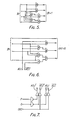
- Figure 1 is a block diagram of the adder circuit;
- Figure 2 shows a set of multiplexers forming part of the adder circuit;
- Figure 3 shows a function control circuit for controlling the multiplexers;
- Figure 4 shows a look-ahead carry circuit;
- Figure 5 shows an incrementer circuit;
- Figure 6 shows a decimal adjustment circuit; and
- Figure 7 shows a decimal adjustment control circuit for controlling the decimal adjustment circuit.
- As shown in Figure 1, the digital adder circuit receives two four-bit operands AO-A3, BO-B3 (where AO and BO are the most significant bits) and produces a four-bit sum output SUM. The circuit also receives a carry-in signal C.
- The circuit is designed to form one stage of a multi-stage adder with look-ahead carry between the stages. This means that, instead of providing a carry-out signal, it produces a carry propagate signal P and a carry generate signal G. The propagate signal P signifies that this stage propagates any carry-in applied to it, i.e. that the carry-in to the next stage should be equal to the carry-in C to this stage. The generate signal G indicates that this stage generates a carry i.e. that the carry-in to the next stage must be one, irrespective of the value of the carry in to this stage. The principles of look-ahead carry addition are well known (see for example an article by O. L. MacSorley entitled "High Speed Arithmetic in Binary Computers, Proceedings of the IRE, January 1961, Pages 67-91) and so will not be described in detail herein.
- The two operands AO-A3, B0B3 are applied to a
binary adder 10, consisting of a group of multiplexers 11 and a look-aheadcarry circuit 12. The multiplexers 11 operate on each corresponding pair of bits Ai, Bi (where i=0, 1, 2, 3) to produce inter-bit propagate and generate signals Pi and Gi. The look-aheadcarry circuit 12 receives these signals and produces a four-bit intermediate result signal IR, and also produces the inter-stage propagate and generate signals P and G. - The multiplexers 11 are controlled by a
function control circuit 13 which is in turn controlled by a set of function control bits FN, and a decimal operation control signal DEC. The signal DEC determines the mode of operation for addition; in a first mode (DEC=0) the operands AO-A3, BO-B3 are treated as binary numbers, whereas in a second mode (DEC=1) they are treated as binary-coded decimal numbers. - In the first mode of operation (DEC=0), the
adder 10 acts as a normal binary look-ahead carry adder. However, in the second mode (DEC=1) the adder forms the sum of the two operands AO-A3, BO-B3 plus a correction value of six (binary 0110). In either case, it should be noted that the addition is performed without any carry-in, since the value of the carry-in signal C is not yet available at this stage of operation. The addition is performed on the assumption that the carry-in is zero. - The intermediate result signal IR is applied to an
incrementer circuit 14 which increments it by one to produce a signal IR+1 which represents the value required for the intermediate result when the carry in C is one. - The signal IR and IR+1 are applied to respective
decimal adjustment circuits 15 and 16 each of which is selectively operable to subtract the decimal correction value of six. Thecircuits 15, 16 are respectively controlled by signals ADJ and ADJ' from a decimal adjustment control circuit 17. This circuit 17 is in turn controlled by the signal DEC and by the inter-stage propagate and generate signals P and G. - The outputs of the
decimal adjustment circuits 15 and 16 are applied to amultiplexer 18, controlled by the carry-in signal C, which selects the output of circuit 15 when C=0, and the output ofcircuit 16 when C=1. The selected signal appears at the output of themultiplexer 18 as the final result SUM. - Referring to Figure 2, the group of multiplexers 11 consists of four pairs of multiplexers MX, one pair for each corresponding pair of operands bits Ai, Bi (i=0, 1, 2, 3). The outputs of each pair represent the corresponding inter-bit generate and propagate signals Gi and Pi.
- As shown, each multiplexer MX has four data bit inputs 0-3, which are connected to receive a four-bit control signal PF, PFX, GF or GFX as shown. These signals are derived from the
function control unit 13. Each multiplexer also has two selection control inputs, which are connected to receive the corresponding operand bits Ai, Bi. - The control signals PF, PFX, GF, GFX are obtained from the
control circuit 13 which is shown in detail in Figure 3. The control circuit derives these signals from an 8-bit function control input signal FN as follows:-PF is derived directly from the four most significant bits of FN. - PFX is derived from the four most significant bits of FN by way of a set of exclusive -OR
gates 30 which are controlled by the decimal mode control signal DEC. When DEC=0, thegates 30 allow signals to pass through without modification so that PFX is equal to PF. When DEC=1, thegates 30 act as inverters and hence PFX is equal to the inverse of PF. - GF is derived directly from the four least significant bits of FN.
- GFX is also derived from the four least significant bits of FN. The first and last bits are derived directly, while the middle two bits pass through two exclusive -OR
gates 31 which invert these two middle bits when DEC=1. - When it is desired to add two operands AO-A3 and BO-B3, the function code FN is given the value 0110 1000 as shown in Figure 3. The resulting values of the control signals are as follows:
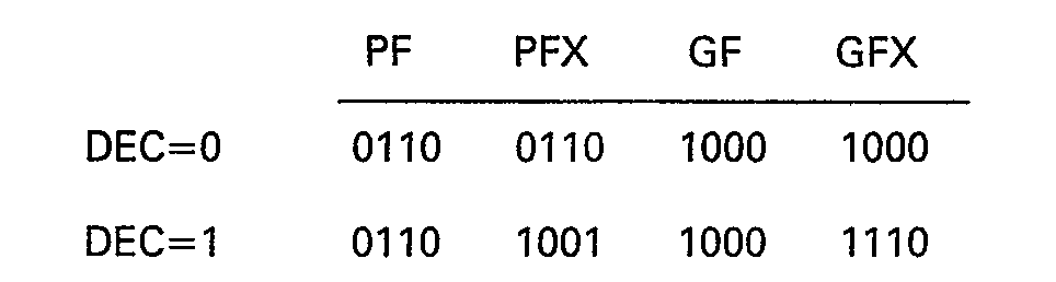
- The resulting patterns of bits applied to the data inputs of the multiplexers MX are shown in Figure 2, in which the first column shows the pattern when DEC=0 (pure binary mode) and the second column shows the pattern when DEC=1 (decimal mode).
- It can readily be seen by inspection of Figure 2 that, when DEC=0, the multiplexers MX are conditioned to produce the correct values for Pi and Gi appropriate to pure binary addition of the two operands, according to the equations


- Similarly, it can be seen that, when DEC=1, the multiplexers are conditioned to produce the correct values of Pi and Gi appropriate to the formation of the sum of the two operands plus the correction value six (binary 0110).
- It should be noted that the addition of the correction value is performed integrally and simultaneously with the addition of the two operands, and hence does not take any extra time.
- The multiplexers 11 are capable of performing operations other than simple addition, by application of different patterns of control bits FN; for example, binary and decimal subtraction and reverse subtraction, multiplication by 2 of either operand, and logical operations. In the case of these logical operations, GF is always set to 0000, DEC is always zero, and the remaining control bits PF determine the logical function to be performed between the operands A and B as follows:-

- By manipulating GF with the PF bits it is possible to combine the logical and arithmetic operations.
- Figure 4 shows the look-
ahead carry circuit 12 in detail. This combines the four pairs of propagate and generate signals Pi, Gi from the multiplexers 11, to produce the intermediate result signal IR, taking account of any inter-bit carries. The circuit caters for the possibility of both Pi and Gi being "1" simultaneously, which can occur in decimal operation. (For simple binary addition Pi and Gi are mutually exclusive). It also produces the inter-stage propagate and generate signals P and G. It is believed that the operation of the look-ahead carry circuit shown in Figure 4 is self-explanatory and so it will not be described in detail herein. - Figure 5 shows the
incrementer circuit 14 in detail. This circuit takes the four-bit intermediate result signal IR and increments it by one to form the signal IR+1. It is believed that the operation of this circuit is self-explanatory. - Figure 6 shows the decimal adjustment circuit 15 in detail. This circuit is controlled by the signal ADJ and its inverse ADJ, from the control circuit 17. When ADJ=0, the output of this circuit equals its input. However, when ADJ=1, the circuit operates to subtract six (binary 0110) from the input. It should be noted that, because of the addition of six performed by the
binary adder 10, the circuit 15 will never be called upon to subtract six from an input value less than six. This simplifies the design of the circuit 15. - The other
decimal adjustment circuit 16 is identical to this circuit, except that the control signal is ADJ' and its inverse ADJ', and the input is IR+1. - Figure 7 shows the decimal adjustment control circuit 7 in detail. This circuit produces the control signals ADJ and ADJ'n(and also their inverses
ADJ andADJ') for the twocorrection circuits 15 and 16. When DEC=0, both ADJ and ADJ' are zero; this is because no decimal adjustment is required in the binary mode of operation. - ADJ=1 whenever DEC=1 and no carry-out is indicated for the
binary adder 10, assuming a carry-in value of C=0. This will be the case if G=O. On the other hand, ADJ'=1 whenever DEC=1 and no carry-out is indicated for thebinary adder 10 assuming a carry-in value of C=1. This will be the case if both G=0 and P=0.
Claims (7)
Applications Claiming Priority (2)
| Application Number | Priority Date | Filing Date | Title |
|---|---|---|---|
| GB8022572 | 1980-07-10 | ||
| GB8022572 | 1980-07-10 |
Publications (2)
| Publication Number | Publication Date |
|---|---|
| EP0044450A1 EP0044450A1 (en) | 1982-01-27 |
| EP0044450B1 true EP0044450B1 (en) | 1985-11-13 |
Family
ID=10514669
Family Applications (1)
| Application Number | Title | Priority Date | Filing Date |
|---|---|---|---|
| EP81105138A Expired EP0044450B1 (en) | 1980-07-10 | 1981-07-02 | Digital adder circuit |
Country Status (5)
| Country | Link |
|---|---|
| US (1) | US4441159A (en) |
| EP (1) | EP0044450B1 (en) |
| AU (1) | AU540899B2 (en) |
| DE (1) | DE3172895D1 (en) |
| ZA (1) | ZA814541B (en) |
Families Citing this family (9)
| Publication number | Priority date | Publication date | Assignee | Title |
|---|---|---|---|---|
| US4707799A (en) * | 1984-01-30 | 1987-11-17 | Kabushiki Kaisha Toshiba | Bit sliced decimal adding/subtracting unit for multi-digit decimal addition and subtraction |
| US4785393A (en) * | 1984-07-09 | 1988-11-15 | Advanced Micro Devices, Inc. | 32-Bit extended function arithmetic-logic unit on a single chip |
| JPS62500474A (en) * | 1985-01-31 | 1987-02-26 | バロ−ス・コ−ポレ−シヨン | High speed BCD/binary adder |
| US5007010A (en) * | 1985-01-31 | 1991-04-09 | Unisys Corp. (Formerly Burroughs Corp.) | Fast BCD/binary adder |
| US5146423A (en) * | 1988-09-09 | 1992-09-08 | Siemens Aktiengesellschaft | Circuit arrangement for adding or subtracting operands coded in BCD-code or binary-code |
| US5673216A (en) * | 1995-12-19 | 1997-09-30 | International Business Machines Corporation | Process and system for adding or subtracting symbols in any base without converting to a common base |
| US6546411B1 (en) | 1999-12-03 | 2003-04-08 | International Business Machines Corporation | High-speed radix 100 parallel adder |
| EP1235109A1 (en) | 2001-02-23 | 2002-08-28 | Infineon Technologies AG | Method for exposing at least one or at least two semiconductor wafers |
| DE102009035290B4 (en) | 2009-07-30 | 2021-07-15 | Carl Zeiss Smt Gmbh | Method and device for determining the relative position of a first structure to a second structure or a part thereof |
Citations (2)
| Publication number | Priority date | Publication date | Assignee | Title |
|---|---|---|---|---|
| US3958112A (en) * | 1975-05-09 | 1976-05-18 | Honeywell Information Systems, Inc. | Current mode binary/bcd arithmetic array |
| US4157589A (en) * | 1977-09-09 | 1979-06-05 | Gte Laboratories Incorporated | Arithmetic logic apparatus |
Family Cites Families (11)
| Publication number | Priority date | Publication date | Assignee | Title |
|---|---|---|---|---|
| US3100835A (en) * | 1960-01-06 | 1963-08-13 | Ibm | Selecting adder |
| US3339064A (en) * | 1962-09-28 | 1967-08-29 | Nippon Electric Co | Decimal addition system |
| US3743824A (en) * | 1971-06-16 | 1973-07-03 | Rca Corp | Carry ripple network for conditional sum adder |
| US3711693A (en) * | 1971-06-30 | 1973-01-16 | Honeywell Inf Systems | Modular bcd and binary arithmetic and logical system |
| DE2352686B2 (en) * | 1973-10-20 | 1978-05-11 | Vereinigte Flugtechnische Werke- Fokker Gmbh, 2800 Bremen | Decimal parallel adder / subtracter |
| US3991307A (en) * | 1975-09-16 | 1976-11-09 | Mos Technology, Inc. | Integrated circuit microprocessor with parallel binary adder having on-the-fly correction to provide decimal results |
| US4172288A (en) * | 1976-03-08 | 1979-10-23 | Motorola, Inc. | Binary or BCD adder with precorrected result |
| JPS5384647A (en) * | 1976-12-30 | 1978-07-26 | Fujitsu Ltd | High-speed adder for binary and decimal |
| US4203157A (en) * | 1978-09-05 | 1980-05-13 | Motorola, Inc. | Carry anticipator circuit and method |
| US4245328A (en) * | 1979-01-03 | 1981-01-13 | Honeywell Information Systems Inc. | Binary coded decimal correction apparatus for use in an arithmetic unit of a data processing unit |
| US4263660A (en) * | 1979-06-20 | 1981-04-21 | Motorola, Inc. | Expandable arithmetic logic unit |
-
1981
- 1981-07-02 DE DE8181105138T patent/DE3172895D1/en not_active Expired
- 1981-07-02 EP EP81105138A patent/EP0044450B1/en not_active Expired
- 1981-07-03 ZA ZA814541A patent/ZA814541B/en unknown
- 1981-07-07 US US06/281,300 patent/US4441159A/en not_active Expired - Lifetime
- 1981-07-09 AU AU72712/81A patent/AU540899B2/en not_active Ceased
Patent Citations (2)
| Publication number | Priority date | Publication date | Assignee | Title |
|---|---|---|---|---|
| US3958112A (en) * | 1975-05-09 | 1976-05-18 | Honeywell Information Systems, Inc. | Current mode binary/bcd arithmetic array |
| US4157589A (en) * | 1977-09-09 | 1979-06-05 | Gte Laboratories Incorporated | Arithmetic logic apparatus |
Also Published As
| Publication number | Publication date |
|---|---|
| AU7271281A (en) | 1982-01-14 |
| US4441159A (en) | 1984-04-03 |
| ZA814541B (en) | 1982-07-28 |
| AU540899B2 (en) | 1984-12-06 |
| EP0044450A1 (en) | 1982-01-27 |
| DE3172895D1 (en) | 1985-12-19 |
Similar Documents
| Publication | Publication Date | Title |
|---|---|---|
| US4707800A (en) | Adder/substractor for variable length numbers | |
| US4866656A (en) | High-speed binary and decimal arithmetic logic unit | |
| JPH05233228A (en) | Floating point arithmetic unit and its arithmetic method | |
| JPH03186924A (en) | Divider | |
| US4878192A (en) | Arithmetic processor and divider using redundant signed digit arithmetic | |
| US4495593A (en) | Multiple bit encoding technique for combinational multipliers | |
| US4805131A (en) | BCD adder circuit | |
| US4441159A (en) | Digital adder circuit for binary-coded numbers of radix other than a power of two | |
| US5195051A (en) | Computation of sign bit and sign extension in the partial products in a floating point multiplier unit | |
| JP3436994B2 (en) | Shift device | |
| US5745399A (en) | Decimal arithmetic apparatus and method | |
| EP0361886B1 (en) | Improved floating point computation unit | |
| US4677583A (en) | Apparatus for decimal multiplication | |
| KR100627993B1 (en) | Three input split-adder | |
| EP0643352A1 (en) | Self-checking complementary adder unit | |
| EP0189912B1 (en) | Fast bcd/binary adder | |
| JPH01302425A (en) | Floating decimal point adder/subtracter circuit | |
| US6546411B1 (en) | High-speed radix 100 parallel adder | |
| JPH076023A (en) | Mantissa addition system for floating-point adder | |
| JPH0374419B2 (en) | ||
| US5432727A (en) | Apparatus for computing a sticky bit for a floating point arithmetic unit | |
| JP2856792B2 (en) | Floating point arithmetic unit | |
| JP2555577B2 (en) | Arithmetic unit | |
| JPH0251732A (en) | Floating point computing element | |
| US5051943A (en) | Adder circuit with an encoded carry |
Legal Events
| Date | Code | Title | Description |
|---|---|---|---|
| PUAI | Public reference made under article 153(3) epc to a published international application that has entered the european phase |
Free format text: ORIGINAL CODE: 0009012 |
|
| 17P | Request for examination filed |
Effective date: 19811012 |
|
| AK | Designated contracting states |
Designated state(s): BE DE FR GB NL |
|
| GRAA | (expected) grant |
Free format text: ORIGINAL CODE: 0009210 |
|
| AK | Designated contracting states |
Designated state(s): BE DE FR GB NL |
|
| REF | Corresponds to: |
Ref document number: 3172895 Country of ref document: DE Date of ref document: 19851219 |
|
| ET | Fr: translation filed | ||
| PLBE | No opposition filed within time limit |
Free format text: ORIGINAL CODE: 0009261 |
|
| STAA | Information on the status of an ep patent application or granted ep patent |
Free format text: STATUS: NO OPPOSITION FILED WITHIN TIME LIMIT |
|
| 26N | No opposition filed | ||
| PGFP | Annual fee paid to national office [announced via postgrant information from national office to epo] |
Ref country code: NL Payment date: 19930731 Year of fee payment: 13 |
|
| PGFP | Annual fee paid to national office [announced via postgrant information from national office to epo] |
Ref country code: DE Payment date: 19930924 Year of fee payment: 13 |
|
| PG25 | Lapsed in a contracting state [announced via postgrant information from national office to epo] |
Ref country code: NL Effective date: 19950201 |
|
| PG25 | Lapsed in a contracting state [announced via postgrant information from national office to epo] |
Ref country code: DE Effective date: 19950401 |
|
| PGFP | Annual fee paid to national office [announced via postgrant information from national office to epo] |
Ref country code: BE Payment date: 19980713 Year of fee payment: 18 |
|
| PGFP | Annual fee paid to national office [announced via postgrant information from national office to epo] |
Ref country code: FR Payment date: 19990615 Year of fee payment: 19 |
|
| PG25 | Lapsed in a contracting state [announced via postgrant information from national office to epo] |
Ref country code: BE Free format text: LAPSE BECAUSE OF NON-PAYMENT OF DUE FEES Effective date: 19990731 |
|
| BERE | Be: lapsed |
Owner name: INTERNATIONAL COMPUTERS LTD Effective date: 19990731 |
|
| PGFP | Annual fee paid to national office [announced via postgrant information from national office to epo] |
Ref country code: GB Payment date: 20000602 Year of fee payment: 20 |
|
| PG25 | Lapsed in a contracting state [announced via postgrant information from national office to epo] |
Ref country code: FR Free format text: LAPSE BECAUSE OF NON-PAYMENT OF DUE FEES Effective date: 20010330 |
|
| REG | Reference to a national code |
Ref country code: FR Ref legal event code: ST |
|
| PG25 | Lapsed in a contracting state [announced via postgrant information from national office to epo] |
Ref country code: GB Free format text: LAPSE BECAUSE OF EXPIRATION OF PROTECTION Effective date: 20010701 |
|
| REG | Reference to a national code |
Ref country code: GB Ref legal event code: PE20 Effective date: 20010701 |