EP0034776B1 - Diagnostic circuit for pcm connection networks - Google Patents
Diagnostic circuit for pcm connection networks Download PDFInfo
- Publication number
- EP0034776B1 EP0034776B1 EP81101030A EP81101030A EP0034776B1 EP 0034776 B1 EP0034776 B1 EP 0034776B1 EP 81101030 A EP81101030 A EP 81101030A EP 81101030 A EP81101030 A EP 81101030A EP 0034776 B1 EP0034776 B1 EP 0034776B1
- Authority
- EP
- European Patent Office
- Prior art keywords
- control device
- decoder
- network
- circuit
- data
- Prior art date
- Legal status (The legal status is an assumption and is not a legal conclusion. Google has not performed a legal analysis and makes no representation as to the accuracy of the status listed.)
- Expired
Links
- 238000012360 testing method Methods 0.000 claims description 32
- 238000012546 transfer Methods 0.000 claims description 13
- 238000003745 diagnosis Methods 0.000 claims description 6
- 230000001360 synchronised effect Effects 0.000 claims description 2
- 230000005284 excitation Effects 0.000 claims 2
- 230000010354 integration Effects 0.000 description 3
- 230000005540 biological transmission Effects 0.000 description 1
- 230000000903 blocking effect Effects 0.000 description 1
- 238000004891 communication Methods 0.000 description 1
- 238000010586 diagram Methods 0.000 description 1
- 230000000694 effects Effects 0.000 description 1
- 238000009432 framing Methods 0.000 description 1
- 238000004519 manufacturing process Methods 0.000 description 1
- 238000012986 modification Methods 0.000 description 1
- 230000004048 modification Effects 0.000 description 1
- 238000012544 monitoring process Methods 0.000 description 1
- 238000012545 processing Methods 0.000 description 1
- 238000011144 upstream manufacturing Methods 0.000 description 1
Images


Classifications
-
- H—ELECTRICITY
- H04—ELECTRIC COMMUNICATION TECHNIQUE
- H04Q—SELECTING
- H04Q11/00—Selecting arrangements for multiplex systems
- H04Q11/04—Selecting arrangements for multiplex systems for time-division multiplexing
Definitions
- the invention relates to a diagnostic circuit arrangement as stated in the prior art portion of claim 1 and is particularly concerned with such diagnostic circuit arrangement for a PCM connection network.
- a diagnostic circuit arrangement as defined in the prior art portion of claim 1 has become known from US-A 4 059 729.
- an extracting circuit serves for picking up the data transferred over a particular channel for monitoring them, or for testing a particular connection by blocking the data transfer therethrough and sending first a loopback code and then a test signal which is looped back and can be checked for possible modification.
- the extracting circuit is connected to a particular control device.
- the control of the extracting circuit has to consider the switching operation with reference to the difference in the channel, frame and group before and after switching and the test start and reset commands with reference to the switching time.
- the respective data are available in the network control device but are not provided for in the prior art arrangement wherein the control device is not that of the network and which does not allow the comparison of the bits of an incoming channel and of the corresponding switched channel.
- the prior art arrangement containing a lot of analog circuitry does not allow integration which however seems almost necessary for the use in larger networks and exchanges.
- the check will be effected by picking up the 8-bit word relating to a channel of an incoming group, whose identity is communicated by the network control device, and by comparing said 8-bit word with the one relating to the switched channel, picked up from the network output after the transit time (frame delay), it too communicated by the control device.
- the aim of the invention is to provide a particular diagnostic circuit arrangement fully useable for diagnosis purpose and comprising extracting circuits easy to integrate which can directly dialogue with the network control microprocessor. This aim is attained by the invention characterized in claim 1.
- the circuit arrangement allows the comparison of the bits of an incoming channel and of the corresponding switched channel of a PCM connection network, e.g. a switching stage.
- Respective ones of the extracting circuits are to be located upstream and downstream the PCM connection network, pick up the content of a channel before and after switching and send it to the control device of the network.
- the extracting circuits being inserted between the lines and the network control device allows the extracting circuits to be synchronized with the time base of the PCM system, receiving therefrom the basic clock signals without need of detecting the framing signals in the data stream.
- the extracting circuit can easily be implemented in a way that allows integration.
- Fig. 1 shows an element RC of a digital connection network equipped with its control device CN and connected to a number of incoming PCM groups FeO...Fei...Fen and the same number of outgoing PCM groups FuO...Fuj...Fun.
- RC is preferably an element of a connection network with a distributed structure, consisting of connection elements realized as integrated circuits, and the control device CN, advantageously consisting of a microprocessor, is the element of the control system of the whole network associated with that particular module for switching control and diagnosis.
- RC may indifferently be either a part of a network or a whole network.
- circuits CT1, CT2 are connected on the one side to incoming groups Fe and outgoing groups Fu respectively and on the other side to bus 1 of the control device; these circuits pick up the 8-bit words relating to a channel of an incoming group and to the corresponding switched outgoing channel and send these words to the control device that is to compare them for diagnosis purposes.
- circuits CT will receive from device CN a number of messages, preferably consisting of 8- bit words, containing the identity of the channel and of the group (incoming or outgoing) concerned in the pick up, the possible frame delay (that is the time necessary to the switching) and the commands relating to the bit transfer to the control device (test start) and to the reset. More particularly, assuming for simplicity of description that there are 16 incoming and/or outgoing groups of 32 channels each, the structure of the messages can be the following:
- circuits CT receive also suitable commands causing the loading of a message coming from control device CN (write) or the transfer to CN of the bits (read) as well as one bit indicating whether the message contains commands (test start, reset) or data (identity of the channel or of the group, frame delay).
- this bit is supposed to be 0 for data messages (words a, b) and 1 for command messages. If the connection network comprises a plurality of elements RC, each equipped with its own circuits CT, the control device will also send enabling signals for the two circuits CT associated with the element under test.
- circuits CT basically comprise:
- Local time base BT receives from a general time base of the switching system signals t 1 corresponding to frame timing (that is signals with period of 125 S, according to the hypotheses made for the number of channels) and signals t 2 corresponding to half the bit time (that is, signals with period of 250 ns), and emits signals t 3 corresponding to the bit time (500 ns) and signals t 4 corresponding to channel time (4 ⁇ s).
- the presence at the input of local time base BT of the signal at 250 ns synchronizes the operating cycle of the pick up circuit with that of the processing unit of the control device.
- selector MX The inputs of selector MX are each connected to one of the incoming groups FeO...Fei...Fen or outgoing groups FuO... Fui...Fun, from which the eight bits of the channel are picked up in series; output 30 is connected to the input of converter SP whose eight output wires 31 are in turn connected to transceiver BD.
- the positioning of the selector is controlled by the bits that identify the group interested in the test; these bits are present on a number of wires of connection 32 outgoing from BD, and are sent to the control input of MX through a parallel-to-parallel register PP belonging to logic network RL.
- a first decoder DE1 receives from CN (through wires 12) and decodes signals that identify which element CT is interested in a test. These signals, which will not be described here in detail because they are not of interest for the invention, will have such a configuration as to allow this decoding to take place completely or mostly in circuit CT and to reduce to a minimum or even eliminate decoding by the control device.
- Output 33 of DE1 is connected to an input of a second decoder DE2.
- DE2 decodes signals RW indicating whether circuit CT is to load a message coming from control device CN via data bus 10 and circuit BD (write) or must transfer the 8-bit word to CN (read). These signals are supplied by CN via wire or connection 13.
- a first output 34 of DE2, energized in case of reading, enables circuit BD to transmission towards CN.
- a second output 35 of DE2, energized in case of writing, enables a third decoder DE3 that receives from BD, via a wire of connection 32, the last bit of each message arriving from CN; besides, decoder DE3 directly receives from CN, via a wire 15, the bit DC indicating whether the message contains data or commands.
- output 36 connected to the "load” of a presettable counter CR1; output 37 connected to the "load” of a second counter CR2 and of register PP; output 38 connected to a circuit SN synchronizing the frame beginning; output 39 connected to the reset of CR1, CR2, SN.
- Outputs 38, 39 are connected to SN or respectively to SN, CR1, CR2 through OR gates P1, P2 that let through on wires 38', 39' either the signals supplied by DE3 or signals of manual test start (SM) or manual reset (RM) present on wires 20, 21.
- Counter CR1 has the data input connected to the wires that in connection 32 convey the bits identifying the channel involved in the test; said bits are loaded when the output 36 of DE3 is energized.
- the clock input of CR1 is connected, through AND gate P3, to that output of BT that carries signals t 4 corresponding to channel timing.
- the transfer of the timing signals to CR1 1 through P3 is enabled by SN, when it receives the signal of beginning of frame (t,).
- the output 40 of CR1, which is activated when CR1 attains its terminal count is connected to a further decoder DE4 and to the clock input of counter CR2.
- Counter CR2 has its data input connected to the wires that in connection 32 convey the bits of the frame delay; said bits will be loaded upon the energization of output 37 of DE3.
- the attainment of the terminal count of CR2 is signalled through wire 41 to decoder DE4 which, upon receiving at the same time a signal from CR1 and CR2, enables the series-to-parallel converters? to load the signals supplied by MX at the rate of signals t 3 .
- Output 42 of DE4 is connected also to a "data ready" circuit DP, that communicates to the control device CN the availability of the data to be transmitted.
- Circuit DP has a second input connected to output 34 of DE2, by which it is disabled when the read command arrives from CN.
- the whole of CR1, CR2 can be realized as a single presettable counter, in which a 8-bit coded value is loaded, where the five least significant bits identify the channel and the other three identify the frame to which the channel belongs.
- the control device when a test is to be effected the control device first sends the information about the identity of the network element involved (via wire 12) and the request for an input-output operation (signal IORQ on wire 14).
- Decoder DE1 recognizing that the test concerns the element CT with which it is associated, enables through wire 33 decoder DE2 having at the input the signal RW present on wire 13 and the request for operation (wire 14).
- the signal on wire 13 will denote that a write operation is to be effected, i.e. that circuit CT is to load the messages present on bus 10.
- Output 35 of DE2 then enables DE3 to decode the last bit of the arriving messages and bit DC (present on wire 15).
- the first message will generally be the reset message.
- bit DC will have value 1 (command) and the last bit of the message will also be 1; output 39 of DE3 will be excited thus resetting the counters and disabling SN.
- the subsequent message will contain the channel identity: it is a data message, then bit DC will be 0. In addition the last bit of this message is 0. Consequently output 36 of DE3 will be excited thus enabling counter CR1 to load the value corresponding to the channel involved. Supposing that the test concerns the m-th channel of incoming group Fei, value 32-m will be set in counter CR1.
- control device CN communicates to the circuit the identity of the group and the frame delay; the last bit of this message is 1 while bit DC is still 0; as a consequence output 37 of DE3 is energized and counter CR2 and register PP are enabled to load the entity of frame delay and the group identity, respectively.
- bit DC passes to a 1 (command) and the last bit of the message is also 1: output 38 of DE3 is excited and it enables SN through P and wire 38': when the "beginning of frame" information arrives from the general time base of the system, P3 is enabled and CR1 begins to count at the rate of the channel timing.
- the terminal count of CR1 is sent through wire 40 to DE4.
- circuit CT1 connected to incoming groups also applies to circuit CT2; the only difference is that a value different from zero is generally set in counter CR2 and therefore decoder DE4 will be enabled after a number of cycles of CR1 and of steps of CR2.
- the messages for CT2 will be sent after those concerning CT1, except the test start, which must be simultaneously sent to both circuits.
- the above description relates to the normal circuit operation, and then all the data and commands are supposed to be sent by the network control device.
- the devices represented as blocks in Fig. 2 will comprise as a whole, in the practical embodiment, about one thousand active components, and the maximum frequency of operation required is 4 MHz (signal t 2 ): both these characteristics are easy to obtain with the present technology of integrated circuit production.
- the circuit presents an 8-wire data bus 10 that can be connected to any commercially available 8-bit microprocessor besides the operation commands (more particularly signals DC, RW and IORQ that denote data/commands, read/write and input-output request) are provided by all known microprocessors.
- operation commands more particularly signals DC, RW and IORQ that denote data/commands, read/write and input-output request
Landscapes
- Engineering & Computer Science (AREA)
- Computer Networks & Wireless Communication (AREA)
- Monitoring And Testing Of Exchanges (AREA)
- Time-Division Multiplex Systems (AREA)
- Use Of Switch Circuits For Exchanges And Methods Of Control Of Multiplex Exchanges (AREA)
Description
- The invention relates to a diagnostic circuit arrangement as stated in the prior art portion of claim 1 and is particularly concerned with such diagnostic circuit arrangement for a PCM connection network.
- A diagnostic circuit arrangement as defined in the prior art portion of claim 1 has become known from US-A 4 059 729. Therein, an extracting circuit serves for picking up the data transferred over a particular channel for monitoring them, or for testing a particular connection by blocking the data transfer therethrough and sending first a loopback code and then a test signal which is looped back and can be checked for possible modification. To this purpose, the extracting circuit is connected to a particular control device.
- To ascertain the good operation of a connection network it is desirable to compare a picked up incoming signal with the picked up switched outgoing signal so as to check the connection continuity and switching correctness. However, to this end, the control of the extracting circuit has to consider the switching operation with reference to the difference in the channel, frame and group before and after switching and the test start and reset commands with reference to the switching time. The respective data are available in the network control device but are not provided for in the prior art arrangement wherein the control device is not that of the network and which does not allow the comparison of the bits of an incoming channel and of the corresponding switched channel. Moreover, the prior art arrangement containing a lot of analog circuitry does not allow integration which however seems almost necessary for the use in larger networks and exchanges.
- In case of a PCM network, the check will be effected by picking up the 8-bit word relating to a channel of an incoming group, whose identity is communicated by the network control device, and by comparing said 8-bit word with the one relating to the switched channel, picked up from the network output after the transit time (frame delay), it too communicated by the control device.
- As the present trend is towards the realization of distributed network structures, that make use of integrated circuits specialized for the various functions and of microprocessors as control devices associated to each network element, it is convenient to distribute among the various network elements also the diagnostic devices; besides such devices ought to be designed according to schemes suitable for the integration (and then allowing an easy arrangement for instance on printed circuit boards, together with the element of connection network and the control devices), and for direct dialogue with the network control microprocessor.
- The aim of the invention is to provide a particular diagnostic circuit arrangement fully useable for diagnosis purpose and comprising extracting circuits easy to integrate which can directly dialogue with the network control microprocessor. This aim is attained by the invention characterized in claim 1.
- By this particular arrangement, the circuit arrangement allows the comparison of the bits of an incoming channel and of the corresponding switched channel of a PCM connection network, e.g. a switching stage. Respective ones of the extracting circuits are to be located upstream and downstream the PCM connection network, pick up the content of a channel before and after switching and send it to the control device of the network. There is no need for either of the two extracting circuits to insert special patterns in the channel, as the data messages sent by the subscribers are used for the diagnosis. In this way the normal operation of the data communication system is undisturbed even for the channel being checked. The extracting circuits being inserted between the lines and the network control device allows the extracting circuits to be synchronized with the time base of the PCM system, receiving therefrom the basic clock signals without need of detecting the framing signals in the data stream. The extracting circuit can easily be implemented in a way that allows integration.
- The foregoing and other characteristics of the invention can in more detail be derived from the subclaims and from the following description of a preferred exemplary embodiment thereof depicted in the annexed drawing in which:
- - Fig. 1 shows the inventive arrangement including the connection of extracting circuits to a PCM connection network;
- - Fig. 2 is a circuit diagram of the extracting circuits.
- Fig. 1 shows an element RC of a digital connection network equipped with its control device CN and connected to a number of incoming PCM groups FeO...Fei...Fen and the same number of outgoing PCM groups FuO...Fuj...Fun.
- RC is preferably an element of a connection network with a distributed structure, consisting of connection elements realized as integrated circuits, and the control device CN, advantageously consisting of a microprocessor, is the element of the control system of the whole network associated with that particular module for switching control and diagnosis.
- For the purposes of the present invention RC may indifferently be either a part of a network or a whole network.
- Two circuits CT1, CT2 are connected on the one side to incoming groups Fe and outgoing groups Fu respectively and on the other side to bus 1 of the control device; these circuits pick up the 8-bit words relating to a channel of an incoming group and to the corresponding switched outgoing channel and send these words to the control device that is to compare them for diagnosis purposes. For these operations circuits CT will receive from device CN a number of messages, preferably consisting of 8- bit words, containing the identity of the channel and of the group (incoming or outgoing) concerned in the pick up, the possible frame delay (that is the time necessary to the switching) and the commands relating to the bit transfer to the control device (test start) and to the reset. More particularly, assuming for simplicity of description that there are 16 incoming and/or outgoing groups of 32 channels each, the structure of the messages can be the following:
- a) channel identity: c, C2 c3 c4 c5 X X 0, where c1...c5 are the bits identifying the channel number, and the letter X indicates a "don't care" condition for the logic value of the respective bit.
- b) group identity and frame delay entity:
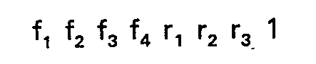
- c) test start: XXXXXXX1 1
- d)reset:XXXXXXX0
- During the various operating steps, circuits CT receive also suitable commands causing the loading of a message coming from control device CN (write) or the transfer to CN of the bits (read) as well as one bit indicating whether the message contains commands (test start, reset) or data (identity of the channel or of the group, frame delay).
- By way of example this bit is supposed to be 0 for data messages (words a, b) and 1 for command messages. If the connection network comprises a plurality of elements RC, each equipped with its own circuits CT, the control device will also send enabling signals for the two circuits CT associated with the element under test.
- Fig. 2 shows that circuits CT basically comprise:
- - a selector MX with a plurality of inputs and one output, followed by a series-to-parallel converter SP, for the transfer to the control device of the bits of the channel under test;
- - a data transceiver BD, by which the circuit is connected to a
data bus 10 to receive the messages and transmit the signals picked up; - - a logic network RL that decodes the messages and the control signals supplied by the control device and controls the pick up and the transfer of the 8-bit words;
- - a local time base BT, timing the operations of the various devices of CT.
- Local time base BT receives from a general time base of the switching system signals t1 corresponding to frame timing (that is signals with period of 125S, according to the hypotheses made for the number of channels) and signals t2 corresponding to half the bit time (that is, signals with period of 250 ns), and emits signals t3 corresponding to the bit time (500 ns) and signals t4 corresponding to channel time (4 αs).

- Slaving the local time base BT to the general time base of the system ensures the synchronization between the two circuits CT1 and CT2 associated with the incoming and outgoing groups of network RC, that is it ensures that the pick up of the bits of the two channels involved in the test takes place exactly in the two corresponding frames.
- More particularly, the presence at the input of local time base BT of the signal at 250 ns synchronizes the operating cycle of the pick up circuit with that of the processing unit of the control device.
- The inputs of selector MX are each connected to one of the incoming groups FeO...Fei...Fen or outgoing groups FuO... Fui...Fun, from which the eight bits of the channel are picked up in series;
output 30 is connected to the input of converter SP whose eightoutput wires 31 are in turn connected to transceiver BD. The positioning of the selector is controlled by the bits that identify the group interested in the test; these bits are present on a number of wires ofconnection 32 outgoing from BD, and are sent to the control input of MX through a parallel-to-parallel register PP belonging to logic network RL. - There, a first decoder DE1 receives from CN (through wires 12) and decodes signals that identify which element CT is interested in a test. These signals, which will not be described here in detail because they are not of interest for the invention, will have such a configuration as to allow this decoding to take place completely or mostly in circuit CT and to reduce to a minimum or even eliminate decoding by the control device.
- In this way the circuit is easy to adapt to variations or extensions of network RC.
-
Output 33 of DE1 is connected to an input of a second decoder DE2. When it is enabled by said output and by the presence of a request for operation (signal IORQ supplied by CN via a wire 14). DE2 decodes signals RW indicating whether circuit CT is to load a message coming from control device CN viadata bus 10 and circuit BD (write) or must transfer the 8-bit word to CN (read). These signals are supplied by CN via wire or connection 13. - A
first output 34 of DE2, energized in case of reading, enables circuit BD to transmission towards CN. - A
second output 35 of DE2, energized in case of writing, enables a third decoder DE3 that receives from BD, via a wire ofconnection 32, the last bit of each message arriving from CN; besides, decoder DE3 directly receives from CN, via a wire 15, the bit DC indicating whether the message contains data or commands. Depending on whether on the message sent by CN contains the channel identity, the group identity and the frame delay, the test start of the reset, there are energized respectively:output 36 connected to the "load" of a presettable counter CR1;output 37 connected to the "load" of a second counter CR2 and of register PP;output 38 connected to a circuit SN synchronizing the frame beginning;output 39 connected to the reset of CR1, CR2, SN.Outputs wires - Counter CR1 has the data input connected to the wires that in
connection 32 convey the bits identifying the channel involved in the test; said bits are loaded when theoutput 36 of DE3 is energized. The clock input of CR1 is connected, through AND gate P3, to that output of BT that carries signals t4 corresponding to channel timing. The transfer of the timing signals to CR1 1 through P3 is enabled by SN, when it receives the signal of beginning of frame (t,). Theoutput 40 of CR1, which is activated when CR1 attains its terminal count is connected to a further decoder DE4 and to the clock input of counter CR2. Counter CR2 has its data input connected to the wires that inconnection 32 convey the bits of the frame delay; said bits will be loaded upon the energization ofoutput 37 of DE3. The attainment of the terminal count of CR2 is signalled through wire 41 to decoder DE4 which, upon receiving at the same time a signal from CR1 and CR2, enables the series-to-parallel converters? to load the signals supplied by MX at the rate of signals t3. -
Output 42 of DE4 is connected also to a "data ready" circuit DP, that communicates to the control device CN the availability of the data to be transmitted. Circuit DP has a second input connected tooutput 34 of DE2, by which it is disabled when the read command arrives from CN. - It is to be noted that in the practical embodiment of the circuit as an integrated circuit, the whole of CR1, CR2 can be realized as a single presettable counter, in which a 8-bit coded value is loaded, where the five least significant bits identify the channel and the other three identify the frame to which the channel belongs.
- The operation of the described circuit is as follows: when a test is to be effected the control device first sends the information about the identity of the network element involved (via wire 12) and the request for an input-output operation (signal IORQ on wire 14). Decoder DE1, recognizing that the test concerns the element CT with which it is associated, enables through
wire 33 decoder DE2 having at the input the signal RW present on wire 13 and the request for operation (wire 14). The signal on wire 13 will denote that a write operation is to be effected, i.e. that circuit CT is to load the messages present onbus 10.Output 35 of DE2 then enables DE3 to decode the last bit of the arriving messages and bit DC (present on wire 15). The first message will generally be the reset message. Under the hypotheses made, bit DC will have value 1 (command) and the last bit of the message will also be 1;output 39 of DE3 will be excited thus resetting the counters and disabling SN. The subsequent message will contain the channel identity: it is a data message, then bit DC will be 0. In addition the last bit of this message is 0. Consequentlyoutput 36 of DE3 will be excited thus enabling counter CR1 to load the value corresponding to the channel involved. Supposing that the test concerns the m-th channel of incoming group Fei, value 32-m will be set in counter CR1. - Subsequently, control device CN communicates to the circuit the identity of the group and the frame delay; the last bit of this message is 1 while bit DC is still 0; as a
consequence output 37 of DE3 is energized and counter CR2 and register PP are enabled to load the entity of frame delay and the group identity, respectively. - An input group is examined, therefore the frame delay will be 0; then CR2 remains stopped on its terminal count (7 according to the hypothesis made at the beginning). In addition selector MX will connect to
output 30 input Fei connected to the homonymous group; circuit SP is not yet enabled, then the bits of the chosen channel cannot yet be transferred to CN. - The last message relates to the "test-start": bit DC passes to a 1 (command) and the last bit of the message is also 1:
output 38 of DE3 is excited and it enables SN through P and wire 38': when the "beginning of frame" information arrives from the general time base of the system, P3 is enabled and CR1 begins to count at the rate of the channel timing. - The terminal count of CR1 is sent through
wire 40 to DE4. - Frame delay has been supposed to be zero and consequently the terminal count of CR2 is already present on wire 41. Under these conditions DE4 enables converter SP to parallelize the bits present on
wire 30, and when the loading is ended, it communicates to CN, through DP, the availability of the bits picked up. Upon receiving the "data ready" from CT1 and CT2 the control device will send the read command: DE2 disables DP and enables transceiver BD, so that the bits are transferred ontobus 10. - What has been described for circuit CT1 connected to incoming groups also applies to circuit CT2; the only difference is that a value different from zero is generally set in counter CR2 and therefore decoder DE4 will be enabled after a number of cycles of CR1 and of steps of CR2.
- The messages for CT2 will be sent after those concerning CT1, except the test start, which must be simultaneously sent to both circuits.
- It is to be noted that while the test is in progress (that is in the time elapsing between the sending of test start and the reception of the data ready from CT2) the control device is available for other operations.
- The above description relates to the normal circuit operation, and then all the data and commands are supposed to be sent by the network control device.
- In certain cases, more particularly during the testing phase, it can be useful to test the circuit without any intervention of the control device.
- To this aim manual reset and test start are utilized; if first the reset command and then the test start command are sent, the circuit will effect the test on channel 0 of group 0, with frame delay zero. The modalites are those described with the exception that the three decoders DE1, DE2, DE3 are not involved in the operation.
- From the previous description the feasibility of the described circuit as an integrated circuit and the ease of dialogue with microprocessor can be deduced.
- In fact the devices represented as blocks in Fig. 2 will comprise as a whole, in the practical embodiment, about one thousand active components, and the maximum frequency of operation required is 4 MHz (signal t2): both these characteristics are easy to obtain with the present technology of integrated circuit production.
- As to the ease of dialogue with microprocessor, the circuit presents an 8-
wire data bus 10 that can be connected to any commercially available 8-bit microprocessor besides the operation commands (more particularly signals DC, RW and IORQ that denote data/commands, read/write and input-output request) are provided by all known microprocessors.
Claims (5)
characterized in that for the diagnosis of a PCM connection network (RC), one of two extracting circuits (CT1, CT2) is each connected between the lines incoming to or outgoing from the connection network, respectively, and the control device which is the network control device (CN) for transfer of the PCM data signals of the two channels connected to each other by the connection network to the network control device, and that within each of the extracting circuits (CT1, CT2) to the output of the selector arrangement (MX) a series-to-parallel converter (SP) is connected to parallelize the bits and has the output connected to an input of a data transceiver (BD), connected on the one hand to a data bus (10) that carries messages coming from the control device (CN) to the extracting circuit (CT1, CT2) and transfers to the control device the bits picked up, and connected on the other hand to the series-to-parallel converter (SP) and the logic network (RL), and that the logic network (RL) comprises:
Applications Claiming Priority (2)
| Application Number | Priority Date | Filing Date | Title |
|---|---|---|---|
| IT6725980 | 1980-02-20 | ||
| IT67259/80A IT1128762B (en) | 1980-02-20 | 1980-02-20 | CIRCUIT FOR DIAGNOSIS OF PCM CONNECTION NETWORKS |
Publications (2)
| Publication Number | Publication Date |
|---|---|
| EP0034776A1 EP0034776A1 (en) | 1981-09-02 |
| EP0034776B1 true EP0034776B1 (en) | 1984-02-01 |
Family
ID=11300923
Family Applications (1)
| Application Number | Title | Priority Date | Filing Date |
|---|---|---|---|
| EP81101030A Expired EP0034776B1 (en) | 1980-02-20 | 1981-02-16 | Diagnostic circuit for pcm connection networks |
Country Status (8)
| Country | Link |
|---|---|
| US (1) | US4404630A (en) |
| EP (1) | EP0034776B1 (en) |
| JP (1) | JPS5948580B2 (en) |
| BR (1) | BR8100788A (en) |
| CA (1) | CA1155241A (en) |
| DE (1) | DE3162066D1 (en) |
| ES (1) | ES497623A0 (en) |
| IT (1) | IT1128762B (en) |
Families Citing this family (12)
| Publication number | Priority date | Publication date | Assignee | Title |
|---|---|---|---|---|
| IT1143268B (en) * | 1981-01-15 | 1986-10-22 | Cselt Centro Studi Lab Telecom | MODULAR STRUCTURE OF DISTRIBUTED CONTROL AND DIAGNOSTIC PCM SWITCHING NETWORK |
| IT1156368B (en) | 1982-06-22 | 1987-02-04 | Cselt Centro Studi Lab Telecom | MODULAR AND SELF-INSTRADING PCM SWITCHING NET FOR DISTRIBUTED COMMON TELEPHONE SELF-SWITCHERS |
| IT1156369B (en) * | 1982-06-22 | 1987-02-04 | Cselt Centro Studi Lab Telecom | MODULAR AND SELF-INSTRADING PCM SWITCHING NETWORK WITH ROAD CONTROL ON VIRTUAL CHANNEL FOR SELF-SWITCHING TELEPHONE WITH DISTRIBUTED CONTROL |
| FR2562368B1 (en) * | 1984-04-02 | 1989-07-28 | Cit Alcatel | SPATIAL CONNECTION NETWORK FOR HIGH SPEED DIGITAL SIGNALS |
| ATE35757T1 (en) * | 1984-04-19 | 1988-07-15 | Siemens Ag | PROCEDURE FOR CONNECTION TESTING OF A ROOM MULTIPLEX COUPLING NETWORK. |
| US4580274A (en) * | 1984-10-02 | 1986-04-01 | The United States Of America As Represented By The Secretary Of The Air Force | Transceiver test device |
| JPS6214372U (en) * | 1985-07-10 | 1987-01-28 | ||
| EP0545482B1 (en) * | 1991-12-04 | 1998-06-24 | Koninklijke Philips Electronics N.V. | Arbiter with a uniformly partitioned architecture |
| ATE158132T1 (en) * | 1992-09-29 | 1997-09-15 | Siemens Ag | METHOD FOR OPERATING THE TIME STAGE ELEMENTS OR COMBINED TIME-SPACE STAGE ELEMENTS OF A COUPLING ARRANGEMENT OF A DIGITAL TIME MULTIPLEX TELECOMMUNICATION EXCHANGE |
| US5835711A (en) * | 1995-02-01 | 1998-11-10 | International Business Machines Corporation | Method and system for implementing multiple leaky bucket checkers using a hybrid synchronous/asynchronous update mechanism |
| US6516291B2 (en) * | 2000-12-13 | 2003-02-04 | Linear Technology Corporation | RMS-to-DC converter with fault detection and recovery |
| TWI424445B (en) * | 2009-12-29 | 2014-01-21 | Macronix Int Co Ltd | Command decoding method and circuit of the same |
Family Cites Families (16)
| Publication number | Priority date | Publication date | Assignee | Title |
|---|---|---|---|---|
| US3920916A (en) * | 1973-09-27 | 1975-11-18 | Stromberg Carlson Corp | Digital switching network |
| FR2252718B1 (en) * | 1973-11-27 | 1978-11-10 | Materiel Telephonique | |
| US3867579A (en) * | 1973-12-21 | 1975-02-18 | Bell Telephone Labor Inc | Synchronization apparatus for a time division switching system |
| GB1492134A (en) * | 1974-04-23 | 1977-11-16 | Wandel & Goltermann | Method of measuring the bit error rate of a regenerated pcm transmission path |
| IT1021020B (en) * | 1974-05-27 | 1978-01-30 | Telettra Lab Telefon | COMMUNICATION SYSTEM AND DEVICES WITH CODED SIGNALS P.C.M. WITH REDUCED REDUNDANCY |
| IT1020712B (en) * | 1974-09-04 | 1977-12-30 | P Belforte | CSELT CENTRO STUDI E LABORATORI TELECOMUNICAZIONI SPA HIGH SPEED ELECTRONIC SWITCHING STAGE FOR CHANNELS NUMBERS CI |
| US4002834A (en) * | 1974-12-09 | 1977-01-11 | The United States Of America As Represented By The Secretary Of The Navy | PCM synchronization and multiplexing system |
| US4001559A (en) * | 1974-12-16 | 1977-01-04 | Northern Telecom, Inc. | Programmable measuring |
| US3959588A (en) * | 1975-05-05 | 1976-05-25 | Gte Automatic Electric Laboratories Incorporated | Digital line synchronizer |
| IT1036311B (en) * | 1975-06-17 | 1979-10-30 | Cselt Centro Studi Lab Telecom | DUPLICATE SYSTEM FOR SUPERVISION AND CONTROL OF DUPLICATED TELECOMMUNICATION SYSTEMS |
| US4059729A (en) * | 1976-06-09 | 1977-11-22 | Martin Marietta Aerospace | Method and system for selectively accessing multiplexed data transmission network for monitoring and testing of the network |
| US4099668A (en) * | 1976-10-29 | 1978-07-11 | Westinghouse Electric Corp. | Monitoring circuit |
| US4112258A (en) * | 1977-10-12 | 1978-09-05 | Bell Telephone Laboratories, Incorporated | Communication system using intelligent network processor |
| FR2379949A1 (en) * | 1977-02-07 | 1978-09-01 | Cii Honeywell Bull | DEVICE FOR CONTROLLING A CONTACT INSERTED BETWEEN A TRANSMITTER CIRCUIT AND A RECEIVER CIRCUIT FOR THE TRANSMISSION OF ELECTRIC SIGNALS |
| US4174805A (en) * | 1978-04-13 | 1979-11-20 | Ncr Corporation | Method and apparatus for transmitting data to a predefined destination bus |
| DE2850652C2 (en) * | 1978-11-22 | 1984-06-28 | Siemens AG, 1000 Berlin und 8000 München | Digital semiconductor circuit |
-
1980
- 1980-02-20 IT IT67259/80A patent/IT1128762B/en active
- 1980-12-11 ES ES497623A patent/ES497623A0/en active Granted
-
1981
- 1981-02-07 JP JP56016328A patent/JPS5948580B2/en not_active Expired
- 1981-02-09 BR BR8100788A patent/BR8100788A/en not_active IP Right Cessation
- 1981-02-16 EP EP81101030A patent/EP0034776B1/en not_active Expired
- 1981-02-16 DE DE8181101030T patent/DE3162066D1/en not_active Expired
- 1981-02-19 CA CA000371285A patent/CA1155241A/en not_active Expired
- 1981-02-19 US US06/235,947 patent/US4404630A/en not_active Expired - Lifetime
Also Published As
| Publication number | Publication date |
|---|---|
| DE3162066D1 (en) | 1984-03-08 |
| IT8067259A0 (en) | 1980-02-20 |
| ES8106992A1 (en) | 1981-09-16 |
| ES497623A0 (en) | 1981-09-16 |
| EP0034776A1 (en) | 1981-09-02 |
| IT1128762B (en) | 1986-06-04 |
| JPS56132039A (en) | 1981-10-16 |
| JPS5948580B2 (en) | 1984-11-27 |
| CA1155241A (en) | 1983-10-11 |
| BR8100788A (en) | 1981-08-25 |
| US4404630A (en) | 1983-09-13 |
Similar Documents
| Publication | Publication Date | Title |
|---|---|---|
| US4646287A (en) | Idle period signalling in a packet switching system | |
| CA1217262A (en) | Data conference arrangement | |
| EP0028437B1 (en) | A high-speed time share processor for use in a data processing system | |
| JPH021652A (en) | Information transmission system | |
| US7050468B2 (en) | Multiplexed signal transmitter/receiver, communication system, and multiplexing transmission method | |
| JPH0127615B2 (en) | ||
| EP0028440B1 (en) | A circuit for handling conversation data in a distributed processing telex exchange | |
| US4143246A (en) | Time division line interface circuit | |
| EP1513306A2 (en) | Interface circuit for zero byte substitution for telecommunications equipment | |
| US4575841A (en) | Method and apparatus for through-connection testing in a digital telecommunication network | |
| EP0028438A1 (en) | An apparatus for generating telex signaling sequences in a distributed processing telex exchange | |
| EP0034776A1 (en) | Diagnostic circuit for PCM connection networks | |
| US3879582A (en) | Data loop communication system | |
| GB1457930A (en) | Digital message switching and transmitting system | |
| JPH02226943A (en) | A system for analyzing and processing high-level data link control procedure frames. | |
| US4551830A (en) | Apparatus for providing loopback of signals where the signals being looped back have an overhead data format which is incompatible with a high speed intermediate carrier overhead format | |
| US5682387A (en) | Demand assign multiplexer providiing efficient demand assign function in multimedia systems having statistical multiplexing transmission | |
| US4191857A (en) | Digital trunk supervisory decoder multiplexor for ground start or E&M signalling on a common T1 span | |
| JPS5810943A (en) | Group multiple address communication system | |
| EP0405041B1 (en) | Terminal adapter having a multiple HDLC communication channels receiver for processing control network management frames | |
| GB2120044A (en) | Auto adjustment of transmission parameters | |
| US5970051A (en) | Reduction of errors in D4 channel bank by multiframe comparison of transmit enable lead to determine whether analog channel unit is installed in D4 channel bank slot | |
| JPH04501943A (en) | Digital transmission link quality inspection equipment | |
| JP3045894B2 (en) | Line fault identification method | |
| WO1987001006A1 (en) | Circuit arrangement to align the pcm groups entering a communication branch point with another |
Legal Events
| Date | Code | Title | Description |
|---|---|---|---|
| PUAI | Public reference made under article 153(3) epc to a published international application that has entered the european phase |
Free format text: ORIGINAL CODE: 0009012 |
|
| AK | Designated contracting states |
Designated state(s): BE CH DE FR GB LI NL SE |
|
| 17P | Request for examination filed |
Effective date: 19811117 |
|
| DET | De: translation of patent claims | ||
| TCNL | Nl: translation of patent claims filed | ||
| TCNL | Nl: translation of patent claims filed | ||
| GRAA | (expected) grant |
Free format text: ORIGINAL CODE: 0009210 |
|
| AK | Designated contracting states |
Designated state(s): BE CH DE FR GB LI NL SE |
|
| REF | Corresponds to: |
Ref document number: 3162066 Country of ref document: DE Date of ref document: 19840308 |
|
| ET | Fr: translation filed | ||
| PLBE | No opposition filed within time limit |
Free format text: ORIGINAL CODE: 0009261 |
|
| STAA | Information on the status of an ep patent application or granted ep patent |
Free format text: STATUS: NO OPPOSITION FILED WITHIN TIME LIMIT |
|
| 26N | No opposition filed | ||
| EAL | Se: european patent in force in sweden |
Ref document number: 81101030.5 |
|
| PGFP | Annual fee paid to national office [announced via postgrant information from national office to epo] |
Ref country code: SE Payment date: 19990204 Year of fee payment: 19 |
|
| PGFP | Annual fee paid to national office [announced via postgrant information from national office to epo] |
Ref country code: BE Payment date: 19990208 Year of fee payment: 19 |
|
| PGFP | Annual fee paid to national office [announced via postgrant information from national office to epo] |
Ref country code: CH Payment date: 19990211 Year of fee payment: 19 |
|
| PGFP | Annual fee paid to national office [announced via postgrant information from national office to epo] |
Ref country code: GB Payment date: 19990218 Year of fee payment: 19 |
|
| PGFP | Annual fee paid to national office [announced via postgrant information from national office to epo] |
Ref country code: FR Payment date: 19990226 Year of fee payment: 19 |
|
| PGFP | Annual fee paid to national office [announced via postgrant information from national office to epo] |
Ref country code: NL Payment date: 19990228 Year of fee payment: 19 |
|
| PGFP | Annual fee paid to national office [announced via postgrant information from national office to epo] |
Ref country code: DE Payment date: 19990427 Year of fee payment: 19 |
|
| PG25 | Lapsed in a contracting state [announced via postgrant information from national office to epo] |
Ref country code: GB Free format text: LAPSE BECAUSE OF NON-PAYMENT OF DUE FEES Effective date: 20000216 |
|
| PG25 | Lapsed in a contracting state [announced via postgrant information from national office to epo] |
Ref country code: SE Free format text: LAPSE BECAUSE OF NON-PAYMENT OF DUE FEES Effective date: 20000217 |
|
| PG25 | Lapsed in a contracting state [announced via postgrant information from national office to epo] |
Ref country code: BE Free format text: LAPSE BECAUSE OF NON-PAYMENT OF DUE FEES Effective date: 20000228 |
|
| PG25 | Lapsed in a contracting state [announced via postgrant information from national office to epo] |
Ref country code: LI Free format text: LAPSE BECAUSE OF NON-PAYMENT OF DUE FEES Effective date: 20000229 Ref country code: CH Free format text: LAPSE BECAUSE OF NON-PAYMENT OF DUE FEES Effective date: 20000229 |
|
| BERE | Be: lapsed |
Owner name: CSELT CENTRO STUDI E LABORATORI TELECOMMUNICAZION Effective date: 20000228 |
|
| PG25 | Lapsed in a contracting state [announced via postgrant information from national office to epo] |
Ref country code: NL Free format text: LAPSE BECAUSE OF NON-PAYMENT OF DUE FEES Effective date: 20000901 |
|
| GBPC | Gb: european patent ceased through non-payment of renewal fee |
Effective date: 20000216 |
|
| EUG | Se: european patent has lapsed |
Ref document number: 81101030.5 |
|
| REG | Reference to a national code |
Ref country code: CH Ref legal event code: PL |
|
| PG25 | Lapsed in a contracting state [announced via postgrant information from national office to epo] |
Ref country code: FR Free format text: LAPSE BECAUSE OF NON-PAYMENT OF DUE FEES Effective date: 20001031 |
|
| NLV4 | Nl: lapsed or anulled due to non-payment of the annual fee |
Effective date: 20000901 |
|
| PG25 | Lapsed in a contracting state [announced via postgrant information from national office to epo] |
Ref country code: DE Free format text: LAPSE BECAUSE OF NON-PAYMENT OF DUE FEES Effective date: 20001201 |
|
| REG | Reference to a national code |
Ref country code: FR Ref legal event code: ST |