EP0033909B1 - Data recording device - Google Patents
Data recording device Download PDFInfo
- Publication number
- EP0033909B1 EP0033909B1 EP81100652A EP81100652A EP0033909B1 EP 0033909 B1 EP0033909 B1 EP 0033909B1 EP 81100652 A EP81100652 A EP 81100652A EP 81100652 A EP81100652 A EP 81100652A EP 0033909 B1 EP0033909 B1 EP 0033909B1
- Authority
- EP
- European Patent Office
- Prior art keywords
- data
- recording device
- display
- address
- camera
- Prior art date
- Legal status (The legal status is an assumption and is not a legal conclusion. Google has not performed a legal analysis and makes no representation as to the accuracy of the status listed.)
- Expired
Links
Images


Classifications
-
- G—PHYSICS
- G03—PHOTOGRAPHY; CINEMATOGRAPHY; ANALOGOUS TECHNIQUES USING WAVES OTHER THAN OPTICAL WAVES; ELECTROGRAPHY; HOLOGRAPHY
- G03B—APPARATUS OR ARRANGEMENTS FOR TAKING PHOTOGRAPHS OR FOR PROJECTING OR VIEWING THEM; APPARATUS OR ARRANGEMENTS EMPLOYING ANALOGOUS TECHNIQUES USING WAVES OTHER THAN OPTICAL WAVES; ACCESSORIES THEREFOR
- G03B17/00—Details of cameras or camera bodies; Accessories therefor
- G03B17/24—Details of cameras or camera bodies; Accessories therefor with means for separately producing marks on the film, e.g. title, time of exposure
-
- G—PHYSICS
- G03—PHOTOGRAPHY; CINEMATOGRAPHY; ANALOGOUS TECHNIQUES USING WAVES OTHER THAN OPTICAL WAVES; ELECTROGRAPHY; HOLOGRAPHY
- G03B—APPARATUS OR ARRANGEMENTS FOR TAKING PHOTOGRAPHS OR FOR PROJECTING OR VIEWING THEM; APPARATUS OR ARRANGEMENTS EMPLOYING ANALOGOUS TECHNIQUES USING WAVES OTHER THAN OPTICAL WAVES; ACCESSORIES THEREFOR
- G03B2217/00—Details of cameras or camera bodies; Accessories therefor
- G03B2217/24—Details of cameras or camera bodies; Accessories therefor with means for separately producing marks on the film
- G03B2217/242—Details of the marking device
- G03B2217/243—Optical devices
Definitions
- This invention relates to a data recording device, and more particularly to a device for previously specifying data to be exposed on a plurality of film frames along with photographic images.
- a camera is fitted with an extra device for recording data on a film with a photographic image.
- the conventional data recording device comprises a light emitting element disposed in a camera behind a film. Before a subject is photographed a desired data is specified. Those segments of a light emitting element which represent a particular data character are made to emit light in synchronization with the photographing of a subject, thereby recording the character on a film together with an image of a subject.
- a particular data has to be specified for each film frame. Where, therefore, the data has to be changed for each frame, the photographing of a subject consumes much time.
- the data recording device comprises the features as characterized in claim 1.
- FIGS. 1A and 1 B are the block circuit diagrams of the data- recording device.
- a switch 10 actuated in response to the wind up of a film is connected at one end to a power supply terminal V cc of 5 volts through a resistor 12, and is grounded at the other end.
- a junction of the switch 10 and resistor 12 is connected to an up-count terminal U of a counter 16, through a resistor 14.
- the up-count terminal U is also grounded through a capacitor 18.
- the power supply terminal V cc is connected to a down-count terminal D of the counter 16.
- a carry terminal CR and borrow terminal BO of the counter 16 are respectively connected to an up-count terminal U and down-count terminal D of a counter 20.
- the counters 16 and 20 are formed of the product SN 74192 of Texas Instrument Co., Inc. (Tl) of America.
- Output terminals QA, QB, QC and QD of the counter 16 and output terminals QA and QB of the counter 20 are respectively connected to terminals PBO to PB5 of a "B port" 24 of a memory device 22.
- the memory device 22 is formed of a static MOS RAM 81 55 of 2,048 bits manufactured by Intel Co., Inc. of America.
- This static MOS RAM 8155 is formed of a combination of a RAM 23, three I/O ports and timer 25.
- a keyboard 32 is connected to a "C port" 36 through a decoder 34.
- the decoder 34 has output terminals representing first to sixth digit positions, which are respectively connected to terminals PCO to PC5 of the "C port" 36.
- a terminal PB6 of the "B port” 24 is connected to J and K input terminals of a shift register 38.
- a terminal PB7 of the "B port” 24 is connected to reset terminal R of the shift register 38.
- a terminal PA6 of the "A port” 30 is connected to J and K input terminals of a shift register 40.
- a terminal PA7 of the "A port” 30 is connected to a reset terminal R of the shift register 40.
- the shift registers 38 and 40 are formed of the product SN 74199 of TI.
- Output terminals QA, QB, QC, QD, QE, QF, QG and QH of the shift register 38 are respectively connected to bases of NPN type transistors 42-1 to 42-8 jointly constituting a driver 42.
- Emitters of the transistors 42-1 to 42-8 are grounded, and collectors thereof are respectively connected to display elements representing eight digit positions which jointly constitute a display section 44.
- the display section 44 is set in a camera behind a film frame to record data related to a foreground subject to be photographed.
- the display elements representing the eight digit positions are each formed of light emitting diodes (LED) constituting seventeen display segments.
- Output terminals QA, QB, QC, OD, QE, QF, QG and QH of the shift register 40 are connected to bases of NPN type transistors 46-1 to 46-8 jointly constituting a driver 46.
- Emitters of the transistors 46-1 to 46-8 are grounded, and collectors thereof are respectively connected to display elements of the display section 48 representing eight digit positions.
- the display section 48 may be set in a finder or at the back of a camera body.
- the display elements representing the eight digit positions are each formed of LEDs constituting seventeen display segments.
- Terminals ADO to AD7 of the memory device 22 are respectively connected to terminals DBO to DB7 of a central processing unit (CPU) 50.
- This CPU 50 is formed of a one-chip microcomputer 8748 of 8 bits manufactured by Intel Co., Inc. of America.
- Terminals P 10 to P12 of the CPU 50 are respectively connected to a system reset terminal RESET, chip enable terminal CE and I/O port and memory selecting terminal 10/M of the memory device 22.
- Terminals P 13 and P 14 of the CPU 50 are respectively connected to first and second movable contacts 54 and 56 of a changeover switch 52.
- a stationary contact 58 of the changeover switch 52 is grounded.
- a terminal P15 of the CPU 50 is grounded through a switch 60.
- Terminals P16 and P17 of the CPU 50 are respectively connected to clock input terminals CK of the shift registers 40 and 38.
- Terminals ALE, RD and WR of the CPU 50 are respectively connected to terminals ALE, RD and WR of the memory device 22.
- Terminals P20 to P26 of the CPU 50 are respectively connected to input terminals of a decoder 62 representing the respective digit positions.
- a terminal P27 of the CPU 50 is connected to a reset terminals of the counters 16 and 20.
- the decoder 62 has seventeen output lines, which are respectively connected to electrodes of the respective segments of the display elements of the display sections 44 and 48 through corresponding buffer amplifiers.
- FIG. 2 is a back view of a camera to which a data recording device embodying this invention is fitted.
- the keyboard 32, changeover switch 52, switch 60 and digital switches 26 and 28 are provided on the backside of the camera.
- the digital switch 26 sends forth a binary coded decimal (BCD) signal of the first place, and the digital switch 28 issues a similarly BCD signal of the second place.
- BCD binary coded decimal
- Display elements which display numerals corresponding to output signals from the digital switches 26 and 28 to determine whether the output signals represent correct values. Each time the digital switches 26 and 28 are operated, numerals represented by output BCD signals therefrom cyclically change between 0 and 9.
- the changeover switch 52 are set at write and reject modes. During the write mode, a first movable contact 54 is connected to a stationary contact 58. During the reject mode, a second movable contact 56 is connected to the stationary contact 58.
- a display section 48 is provided above the keyboard 32.
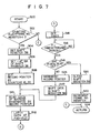
- a data recording device embodying this invention First with reference to the flow chart of the CPU 50 shown in Figure 3.
- a reset routine 102 is carried out.
- the counters and shift registers are set at the initial state.
- a step 104 judgement is made as to whether the switch 60 is closed. Where the switch 60 is closed, a data recording routine 106 is performed. Where the switch 60 is left open, judgement is made at a step 108 as to whether the changeover switch 52 is set at the write mode. Where the data recording routine 106 is brought to an end, then the step 104 is again taken.
- a data writing routine 110 is carried out.
- a read pointer of the CPU 50 is set to designate the foremost address of a memory region of the RAM 23, which corresponds to a number jointely represented by output BCD signals from the digital switches 26 and 28.
- the read pointer is provided on software and designates the read address of the RAM 23.
- the digital switches-26 and 28 are so set as to indicate the serial number of a film frame on which data is to be recorded.
- the read pointer of the CPU 50 is set to designate the foremost address of a memory region of the RAM 23 corresponding to a number jointly represented by output signals from the counters 16 and 20 at a step 114.
- One memory region of the RAM 23 of the CPU 50 has eight addresses, in each of which a signal representing any of the aforementioned 39 characters is stored.
- a data display routine 116 is carried out. Where this data display routine 116 is brought to an end, the step 104 is resumed.
- the CPU 50 is cyclically operated while sensing the conditions of the switch 60 and changeover switch 52. The fitting of a film to a camera and an operation undertaken after the exposure of all film frames which are not related to this invention are omitted from Figure 3.
- FIG. 4 is a detailed flow chart of the reset routine 102.
- a frame number register of the CPU 50 which is provided on software and determines whether a data has been recorded on a given film frame, is set at zero at a step 202 immediately following the starting step 200.
- the counters 16 and 20 are reset at zero.
- An output signal from the counter 16 represents a 10- scale number of the first place.
- An output signal from the counter 20 denotes a similarly 10- scale number of the second place.
- the reset routine 102 is brouqht to end.
- FIG. 5 is a detailed flow chart of the data writing routine 110.
- the CPU 50 reads output signals from the digital switches 26 and 28 through the A port 30.
- a write pointer is set to designate the foremost address of a memory region of the RAM 23 which corresponds to a number jointly expressed by output signals from the digital switches 26 and 28. This write pointer is provided on software, and designates a desired write address of the RAM 23.
- judgement is made as to whether any key of the keyboard 32 has been depressed. Where it is found that no key is depressed, then the step 306 is shifted to a step 308, bringing a data writing routine to an end.
- any key of the keyboard 32 is depressed, then judgement is made whether the depressed key is the CL key at a step 310. Where the CL key is depressed, then eight data of the RAM regions which corresponds to a number jointly represented by output signals from the digital switches 26 and 28, namely, which is designated by the write pointer are cleared at a step 312. Thereafter, the step 302 is again carried out.
- the CL key is a clear key and is used to clear, if necessary, the data which are to be recorded on a film frame specified by a number jointly denoted by output signals from the digital switches 26 and 28. Where the CL key is not depressed, then judgement is made as to whether a key depressed is a CE key at a step 314.
- step 316 judgement is made at a step 316 as to whether the write pointer designates the foremost address of a given RAM region comprising eight addresses which corresponds to a number jointly'denoted by output signals from the digital switches 26 and 28. Where the write pointer designates the foremost address, then the step 306 is again taken. Conversely where the write pointer does not designate the foremost address, then a number of 1 is decreased from the serial number of an address designated by the write pointer at a step 318. Data stored in an address designated by the write pointer is cleared at a step 320. Where the step 320 is brought to an end, the step 306 is again taken.
- FIG. 6 is a detailed flow chart of the data display routine 116 of Figure 3.
- the shift register 40 is released from a cleared state at a step 402 immediately following a starting step 400. Namely, the CPU 50 supplies a reset- releasing signal to the reset terminal R of the shift register 40 through the A port 30.
- the terminal QA of the shift register 40 is set at a level "1". As a result, only a transistor 46-8 included in the driver 46 is rendered conducting, thereby making the display element of the first digit position of the display section 48 ( Figure 3) ready for display.
- a 16-scale ASCII code having two digit positions is read out from that address of the RAM 23 which is designated by a read pointer.
- the ASCII code is latched by a latch section (constituted by terminals P20 to P27).
- the decoder 62 decodes the ASCII code, thereby actuating the selected segments of a display element.
- the decoder 62 comprises seventeen output terminals a to q . corresponding to the seventeen segments A to Q of each display element.
- a timer 25 is energized at a step 410.
- judgement is made as to whether a prescribed length of time has passed.
- the term "prescribed length of time” means a period for defining a display time per digit position. This display time is chosen to last for less than 2 milliseconds in order to prevent the occurrence of flickerings.
- judgement is made as to whether eight data have been read out from the RAM region. If this is the case, the shift register 40 is cleared at a step 416.
- the data display routine is brought to an end.
- the read pointer designates at a step 420 a new address which bears a serial number larger by 1 than that of the address which was previously designated by the read pointer.
- a data "1" stored in the shift register 40 is displaced by one digit position.
- a transistor included in the driver 46 which was rendered conducting up to this point is unactuated.
- a new transistor adjacent to the preceding transistor is now rendered conducting.
- the display element of the display section 48 which is to emit light is displaced by one digit position.
- the step 406 is resumed.
- Data stored in the RAM 23 is dynamically indicated on the display section 48, enabling the operator of the data recording device to recognize recorded data with great ease.
- FIG. 7 is a detailed flow chart of the data recording routine 106 of Figure 3.
- a step 502 immediately following the starting step 500, judgement is made as to whether a number jointly denoted by output signals from the counters 16 and 20 represents a number equal to a sum of a value stored in the film frame number register of the CPU 50 and a number of 1.
- the switch 10 connected the up-count terminal U of the counter 16 is closed interlockingly with the winding up of a film. Therefore, a number jointly represented output signals from the counters 16 and 20 represent a number of film frames which have been photographed.
- the aforementioned judgement proves the presence of coincidence between the number jointly denoted by output signals from the counters 16 and 20 and a sum of a value stored in the film frame number register and a number of 1, then a film frame brought behind the camera shutter at this point is shown to be the right one on which a new data is to be recorded.
- the shift register 38 is released from its cleared state.
- the terminal QA of the shift register 38 is set at a level "1 ". Accordingly, only a transistor 42-1 included in the driver 42 is rendered conducting, causing the display element of the first digit position of the display section 44 to get ready for display.
- a number of an address designated by a record pointer is made to represent that of the foremost address of the RAM region corresponding to a number jointly represented by output signals from the counters 16 and 20.
- Data (16-scale ASCII code having two digit positions) read out from the addresses of the RAM 23 which is designated by the record pointer at a step 510 is latched by the latch section of the CPU 50 at a step 512.
- data stored in the RAM 23 is indicated by the display section 44 as in the data display routine 116 of Figure 3.
- a timer 25 is energized.
- judgement is made as to whether a prescribed length of time has passed.
- the prescribed length of time defines a period during which the display section 44 is allowed to emit light.
- the prescribed length of time is so chosen as to enable data to be recorded on a film frame with a proper degree of exposure in accordance with the sensitivity of a film and the intensity of light emitted by the display element.
- a number indicated by the record pointer is increased by 1 at a step 526, thereby causing the data stored in the shift register 38 to be shifted by one digit position at a step of 528. That of the transistors of the driver 42 which was previously rendered conducting is now unactuated. A new transistor adjacent to the transistor is put into operation, causing light to be emitted while the display elements of the display section 44 are successively displaced by one digit position. In other words, the display section 44 carries out a dynamic display. After the step 528, the step 510 is resumed. As described above, data stored in the RAM 23 are recorded on a film frame in response to the depression of a release button.
- step 502 Where it is judged at the step 502 that no coincidence takes place between a number jointly denoted by the counts may by the counters 16 and 20 and a sum of a value stored in the film frame number register and a number of 1, then the step 524 is immediately taken.
- a data is recorded on a film frame when, for example, a coeliac foreground subject is photographed by an endoscope.
- 24 film frames have been photographed, and four items of data as 81-02-04, HATTORI, CLE-F and TGF-2T are to be respectively recorded on the 25th to 28th film frames.
- the data recorded on the 25th film frame is a date of photographing
- the data recorded on the 26th film frame is a patient's name
- the data recorded on the 27th indicates the type of an endoscope light source
- the data recorded on the 28th film frame shows the type of an endoscope itself.
- the photographer first sets the changeover switch 52 at the write mode.
- An output signal from the digital switch 28 is chosen to indicate "2".
- An output signal from the digital switch 26 is chosen to indicate "5". It is further assumed that the switch 60 is of the normally open type and is still left open at this moment. Accordingly, the data writing routine 110 of Figure 3 is carried out. Where the photographer supplies an input "HATTORI” by operating the keyboard 32, then an ASCII code representing "HATTORI" is stored in that region of the RAM 23 which corresponds to the 25th film frame. After recording the data "HATTORI", the photographer depresses the CR key, thereby reporting to the CPU 50 that data recording has been brought to an end.
- the data display routine 116 is carried out. As a result, "HATTORI" is displayed on the display section 48. Thereafter, the data writing routine 110 is resumed, causing data to be recorded on those of the RAM regions which correspond to the 26th, 27th and 28th film frames, where output signals of the digital switches 28 and 26 are changed.
- the read pointer designates at the step 114 a value corresponding to a number jointly represented by output signals from the counters 16 and 20 (for example, a number of "25", because, in the aforementioned case, 24 film frames have been photographed).
- the counters 16 and 20 are set at "1", thereby getting ready to indicate a number of film frames to be photographed later.
- the data display routine 116 Figure 3 data stored in the RAM region corresponding to the 25th film frame (that is, "HATTORI" in the aforementioned example) are displayed. After confirming the displayed data, the photographer closes the switch 60, thereby allowing for the execution of the data recording routine 106 ( Figure 3).
- a number stored in the frame number register is progressively increased by 1 as data recording proceeds. Then a number of "24" is stored in the register.
- the steps 504 and 506 are carried out after the step 502, thereby setting the terminal QA of the shift register 38 at a level "1".
- the read pointer designates a number of "25”.
- data "HATTORI” is read out of the RAM region corresponding to the 25th film frame.
- a number of 25 is stored in the frame number register.
- judgement of "NO” is given, thereby preventing data recording from being undertaken.
- a data recording device embodying this invention data to be recorded on a plurality of film frames can be previously specified, effecting the recording quickly without prolonging photographing time.
- the aforementioned embodiment is not limited to the photographing of a coeliac cavity by an endoscope.
- the switch 60 is left open at the shutter release, no data is recorded on any film frame. Later when the switch 60 is closed, specified data can be recorded on a film frame.
Abstract
Description
- This invention relates to a data recording device, and more particularly to a device for previously specifying data to be exposed on a plurality of film frames along with photographic images.
- A camera is fitted with an extra device for recording data on a film with a photographic image. The conventional data recording device comprises a light emitting element disposed in a camera behind a film. Before a subject is photographed a desired data is specified. Those segments of a light emitting element which represent a particular data character are made to emit light in synchronization with the photographing of a subject, thereby recording the character on a film together with an image of a subject. With the prior art data recording device, a particular data has to be specified for each film frame. Where, therefore, the data has to be changed for each frame, the photographing of a subject consumes much time. Particularly where a subject is photographed by an endoscope, it is necesary to record on a film many items of data such as a date, patient's name, number of a patient's chart and photographed coeliac portion, thus consuming a great deal of time. Where data has to be changed for each frame, examination by an endoscope takes much time, causing great pain to a patient. With the conventional data recording device, data items can not be selected with a sufficient margin of time, resulting in the possibility of recording wrong data or missing a chance while data is checked.
- It is accordingly the object of this invention to provide a data recording device which can be provided with a sufficient amount of data to be exposed on a plurality of film frames, thereby enabling correct data to be recorded quickly and shortening the total photographing time.
- To attain the above object, the data recording device comprises the features as characterized in
claim 1. - This invention can be more fully understood from the following detailed description when taken in conjunction with the accompanying drawings, in which:
- Figures 1 A and 1 B are block circuit diagrams of a data recording device embodying this invention;
- Figure 2 is a back view of a camera to which the data recording device of this invention is fitted;
- Figure 3 is a flow chart showing the operation modes of the data recording device of this invention;
- Figure 4 is a detailed flow chart of a reset routine included in the flow chart of Figure 3;
- Figure 5 is a detailed flow chart of a data writing routine included in the flow chart of Figure 3;
- Figure 6 is a detailed flow chart of a data display routine included in the flow chart of Figure 3; and
- Figure 7 is a detailed flow chart of a data recording routine included in the flow chart of Figure 3.
- Description is now given with reference to the accompanying drawings of a data recording device embodying this invention. Figures 1A and 1 B are the block circuit diagrams of the data- recording device. A
switch 10 actuated in response to the wind up of a film is connected at one end to a power supply terminal Vcc of 5 volts through a resistor 12, and is grounded at the other end. A junction of theswitch 10 and resistor 12 is connected to an up-count terminal U of acounter 16, through a resistor 14. The up-count terminal U is also grounded through a capacitor 18. The power supply terminal Vcc is connected to a down-count terminal D of thecounter 16. A carry terminal CR and borrow terminal BO of thecounter 16 are respectively connected to an up-count terminal U and down-count terminal D of acounter 20. Thecounters counter 16 and output terminals QA and QB of thecounter 20 are respectively connected to terminals PBO to PB5 of a "B port" 24 of amemory device 22. Thememory device 22 is formed of a static MOS RAM 81 55 of 2,048 bits manufactured by Intel Co., Inc. of America. This static MOS RAM 8155 is formed of a combination of aRAM 23, three I/O ports andtimer 25. Four output terminals of adigital switch 26 representing first to fourth digit positions are respectively connected to terminals PAO to PA3 of an "A port" 30. Two output terminals of adigital switch 28 representing first and second digit positions are respectively connected to terminals PA4 and PA5 of the "A port" 30. Akeyboard 32 is connected to a "C port" 36 through adecoder 34. - The
decoder 34 has output terminals representing first to sixth digit positions, which are respectively connected to terminals PCO to PC5 of the "C port" 36. - A terminal PB6 of the "B port" 24 is connected to J and K input terminals of a
shift register 38. A terminal PB7 of the "B port" 24 is connected to reset terminal R of theshift register 38. A terminal PA6 of the "A port" 30 is connected to J and K input terminals of ashift register 40. A terminal PA7 of the "A port" 30 is connected to a reset terminal R of theshift register 40. Theshift registers shift register 38 are respectively connected to bases of NPN type transistors 42-1 to 42-8 jointly constituting adriver 42. Emitters of the transistors 42-1 to 42-8 are grounded, and collectors thereof are respectively connected to display elements representing eight digit positions which jointly constitute adisplay section 44. Thedisplay section 44 is set in a camera behind a film frame to record data related to a foreground subject to be photographed. The display elements representing the eight digit positions are each formed of light emitting diodes (LED) constituting seventeen display segments. Output terminals QA, QB, QC, OD, QE, QF, QG and QH of theshift register 40 are connected to bases of NPN type transistors 46-1 to 46-8 jointly constituting adriver 46. Emitters of the transistors 46-1 to 46-8 are grounded, and collectors thereof are respectively connected to display elements of thedisplay section 48 representing eight digit positions. Thedisplay section 48 may be set in a finder or at the back of a camera body. The display elements representing the eight digit positions are each formed of LEDs constituting seventeen display segments. - Terminals ADO to AD7 of the
memory device 22 are respectively connected to terminals DBO to DB7 of a central processing unit (CPU) 50. ThisCPU 50 is formed of a one-chip microcomputer 8748 of 8 bits manufactured by Intel Co., Inc. of America.Terminals P 10 to P12 of theCPU 50 are respectively connected to a system reset terminal RESET, chip enable terminal CE and I/O port andmemory selecting terminal 10/M of thememory device 22. Terminals P 13 and P 14 of theCPU 50 are respectively connected to first and secondmovable contacts changeover switch 52. Astationary contact 58 of thechangeover switch 52 is grounded. A terminal P15 of theCPU 50 is grounded through aswitch 60. Terminals P16 and P17 of theCPU 50 are respectively connected to clock input terminals CK of theshift registers CPU 50 are respectively connected to terminals ALE, RD and WR of thememory device 22. Terminals P20 to P26 of theCPU 50 are respectively connected to input terminals of adecoder 62 representing the respective digit positions. A terminal P27 of theCPU 50 is connected to a reset terminals of thecounters decoder 62 has seventeen output lines, which are respectively connected to electrodes of the respective segments of the display elements of thedisplay sections - Figure 2 is a back view of a camera to which a data recording device embodying this invention is fitted. The
keyboard 32,changeover switch 52,switch 60 anddigital switches digital switch 26 sends forth a binary coded decimal (BCD) signal of the first place, and thedigital switch 28 issues a similarly BCD signal of the second place. Provided near thedigital switches digital switches digital switches changeover switch 52 are set at write and reject modes. During the write mode, a firstmovable contact 54 is connected to astationary contact 58. During the reject mode, a secondmovable contact 56 is connected to thestationary contact 58. Adisplay section 48 is provided above thekeyboard 32. - Description is now given of the operation of a data recording device embodying this invention, first with reference to the flow chart of the
CPU 50 shown in Figure 3. At a startingstep 100, power is supplied to the data recording device, and then areset routine 102 is carried out. At thereset routine 102, the counters and shift registers are set at the initial state. At astep 104, judgement is made as to whether theswitch 60 is closed. Where theswitch 60 is closed, adata recording routine 106 is performed. Where theswitch 60 is left open, judgement is made at a step 108 as to whether thechangeover switch 52 is set at the write mode. Where the data recording routine 106 is brought to an end, then thestep 104 is again taken. Where thechangeover switch 52 is set at the write mode, then a data writing routine 110 is carried out. At a succeedingstep 112, a read pointer of theCPU 50 is set to designate the foremost address of a memory region of theRAM 23, which corresponds to a number jointely represented by output BCD signals from thedigital switches RAM 23. The digital switches-26 and 28 are so set as to indicate the serial number of a film frame on which data is to be recorded. Where thechangeover switch 52 is not set at the write mode, but at the reject mode, then the read pointer of theCPU 50 is set to designate the foremost address of a memory region of theRAM 23 corresponding to a number jointly represented by output signals from thecounters RAM 23 of theCPU 50 has eight addresses, in each of which a signal representing any of the aforementioned 39 characters is stored. After thestep 112 or 114, adata display routine 116 is carried out. Where thisdata display routine 116 is brought to an end, thestep 104 is resumed. As described above, theCPU 50 is cyclically operated while sensing the conditions of theswitch 60 andchangeover switch 52. The fitting of a film to a camera and an operation undertaken after the exposure of all film frames which are not related to this invention are omitted from Figure 3. - Detailed description is now given of the respective routines of Figure 3. Figure 4 is a detailed flow chart of the
reset routine 102. A frame number register of theCPU 50 which is provided on software and determines whether a data has been recorded on a given film frame, is set at zero at astep 202 immediately following the startingstep 200. At astep 204, thecounters counter 16 represents a 10- scale number of the first place. An output signal from thecounter 20 denotes a similarly 10- scale number of the second place. At thestep 206, data stored in the shift registers 38 and 40 are cleared. At astep 208, thereset routine 102 is brouqht to end. - Figure 5 is a detailed flow chart of the data writing routine 110. At a
step 302 immediately following a startingstep 300, theCPU 50 reads output signals from thedigital switches A port 30. At astep 304, a write pointer is set to designate the foremost address of a memory region of theRAM 23 which corresponds to a number jointly expressed by output signals from thedigital switches RAM 23. At astep 306, judgement is made as to whether any key of thekeyboard 32 has been depressed. Where it is found that no key is depressed, then thestep 306 is shifted to astep 308, bringing a data writing routine to an end. Where it is found that any key of thekeyboard 32 is depressed, then judgement is made whether the depressed key is the CL key at astep 310. Where the CL key is depressed, then eight data of the RAM regions which corresponds to a number jointly represented by output signals from thedigital switches step 312. Thereafter, thestep 302 is again carried out. The CL key is a clear key and is used to clear, if necessary, the data which are to be recorded on a film frame specified by a number jointly denoted by output signals from thedigital switches step 314. Where the CE key is depressed, then judgement is made at astep 316 as to whether the write pointer designates the foremost address of a given RAM region comprising eight addresses which corresponds to a number jointly'denoted by output signals from thedigital switches step 306 is again taken. Conversely where the write pointer does not designate the foremost address, then a number of 1 is decreased from the serial number of an address designated by the write pointer at astep 318. Data stored in an address designated by the write pointer is cleared at astep 320. Where thestep 320 is brought to an end, thestep 306 is again taken. In other words, where the CE key is depressed, then only a character supplied by a key depressed immediately before the depression of the CE key is cleared. Where the CE key is not depressed, then judgement is made as to whether a key depressed is a CR key at astep 322. Where the CR key is depressed, then a "NULL" is stored at astep 324 in a RAM region which follow an address designated by the write pointer. At thestep 308, the data writing routine is brought to an end. Unless the CR key is depressed, a data supplied by a key depressed at astep 326 is stored in an address designated by the write pointer. - Where an ASCII code signal corresponding to a depressed key is stored in the
RAM 23, then judgement is made as to whether data have been stored in the whole of a RAM region designated by a write pointer, that is, the eight addresses of the RAM region have all been supplied with data. Where all the eight addresses are supplied with data, then thestep 306 is resumed. Conversely where eight data are not supplied to the RAM region, then astep 330 is taken to designate a new address which bears a serial number larger by 1 than that of the address previously designated by the write pointer. Thereafter, thestep 306 is taken again. Every eight characters of data are stored in the eight addresses of each RAM region. - Figure 6 is a detailed flow chart of the
data display routine 116 of Figure 3. Theshift register 40 is released from a cleared state at astep 402 immediately following a startingstep 400. Namely, theCPU 50 supplies a reset- releasing signal to the reset terminal R of theshift register 40 through theA port 30. At astep 404, the terminal QA of theshift register 40 is set at a level "1". As a result, only a transistor 46-8 included in thedriver 46 is rendered conducting, thereby making the display element of the first digit position of the display section 48 (Figure 3) ready for display. At astep 406, a 16-scale ASCII code having two digit positions is read out from that address of theRAM 23 which is designated by a read pointer. At astep 408, The ASCII code is latched by a latch section (constituted by terminals P20 to P27). Thedecoder 62 decodes the ASCII code, thereby actuating the selected segments of a display element. Thedecoder 62 comprises seventeen output terminals a to q. corresponding to the seventeen segments A to Q of each display element. - A
timer 25 is energized at astep 410. At astep 412, judgement is made as to whether a prescribed length of time has passed. As used herein, the term "prescribed length of time" means a period for defining a display time per digit position. This display time is chosen to last for less than 2 milliseconds in order to prevent the occurrence of flickerings. At astep 414, judgement is made as to whether eight data have been read out from the RAM region. If this is the case, theshift register 40 is cleared at astep 416. At astep 418, the data display routine is brought to an end. Where eight data are not read out from the RAM region, then the read pointer designates at a step 420 a new address which bears a serial number larger by 1 than that of the address which was previously designated by the read pointer. At astep 422, a data "1" stored in theshift register 40 is displaced by one digit position. As a result, a transistor included in thedriver 46 which was rendered conducting up to this point is unactuated. A new transistor adjacent to the preceding transistor is now rendered conducting. Thus, the display element of thedisplay section 48 which is to emit light is displaced by one digit position. Where thestep 422 is brought to an end, thestep 406 is resumed. Data stored in theRAM 23 is dynamically indicated on thedisplay section 48, enabling the operator of the data recording device to recognize recorded data with great ease. - Figure 7 is a detailed flow chart of the
data recording routine 106 of Figure 3. At astep 502 immediately following the startingstep 500, judgement is made as to whether a number jointly denoted by output signals from thecounters CPU 50 and a number of 1. Theswitch 10 connected the up-count terminal U of thecounter 16 is closed interlockingly with the winding up of a film. Therefore, a number jointly represented output signals from thecounters counters step 504, theshift register 38 is released from its cleared state. At astep 506 the terminal QA of theshift register 38 is set at a level "1 ". Accordingly, only a transistor 42-1 included in thedriver 42 is rendered conducting, causing the display element of the first digit position of thedisplay section 44 to get ready for display. At a step 508 a number of an address designated by a record pointer is made to represent that of the foremost address of the RAM region corresponding to a number jointly represented by output signals from thecounters RAM 23 which is designated by the record pointer at astep 510 is latched by the latch section of theCPU 50 at astep 512. As a result, data stored in theRAM 23 is indicated by thedisplay section 44 as in thedata display routine 116 of Figure 3. At a step 514 atimer 25 is energized. At astep 516, judgement is made as to whether a prescribed length of time has passed. The prescribed length of time defines a period during which thedisplay section 44 is allowed to emit light. The prescribed length of time is so chosen as to enable data to be recorded on a film frame with a proper degree of exposure in accordance with the sensitivity of a film and the intensity of light emitted by the display element. After the prescribed length of time, judgement is made at astep 518 as to whether eight data have been read out from the RAM region. If this is the case, theshift register 38 is cleared at astep 520. After a value stored in the frame number register is increased by 1 at astep 522, the data recording routine is brought to an end at astep 524. Where eight data are not read out from the RAM region, then a number indicated by the record pointer is increased by 1 at astep 526, thereby causing the data stored in theshift register 38 to be shifted by one digit position at a step of 528. That of the transistors of thedriver 42 which was previously rendered conducting is now unactuated. A new transistor adjacent to the transistor is put into operation, causing light to be emitted while the display elements of thedisplay section 44 are successively displaced by one digit position. In other words, thedisplay section 44 carries out a dynamic display. After thestep 528, thestep 510 is resumed. As described above, data stored in theRAM 23 are recorded on a film frame in response to the depression of a release button. Where it is judged at thestep 502 that no coincidence takes place between a number jointly denoted by the counts may by thecounters step 524 is immediately taken. - Description is now given of a concrete example where a data is recorded on a film frame when, for example, a coeliac foreground subject is photographed by an endoscope. Now let it be assumed that 24 film frames have been photographed, and four items of data as 81-02-04, HATTORI, CLE-F and TGF-2T are to be respectively recorded on the 25th to 28th film frames. Further let it be supposed that the data recorded on the 25th film frame is a date of photographing, the data recorded on the 26th film frame is a patient's name, the data recorded on the 27th indicates the type of an endoscope light source, and the data recorded on the 28th film frame shows the type of an endoscope itself. The photographer first sets the
changeover switch 52 at the write mode. An output signal from thedigital switch 28 is chosen to indicate "2". An output signal from thedigital switch 26 is chosen to indicate "5". It is further assumed that theswitch 60 is of the normally open type and is still left open at this moment. Accordingly, thedata writing routine 110 of Figure 3 is carried out. Where the photographer supplies an input "HATTORI" by operating thekeyboard 32, then an ASCII code representing "HATTORI" is stored in that region of theRAM 23 which corresponds to the 25th film frame. After recording the data "HATTORI", the photographer depresses the CR key, thereby reporting to theCPU 50 that data recording has been brought to an end. Where it is found that the wrong key has been depressed, then a process characters one by one or depressing the CL key to erase data items stored in all the addresses of the RAM region. Where eight data are stored in all the address of the RAM region, thedata writing routine 110 of Figure 3 is brought to an end. Where it is necessary to provide a blank between two adjacent characters, it is advised to supply thekeyboard 32 with a BLANK key. In this case, all the input terminals a to m of thedecoder 34 are set a level "0" in response to the depression of the BLANK key, thereby allowing for the emission of theASCII code 20. - After the read pointer designates the foremost address of that region of the
RAM 23 which corresponds to the 25th film frame at thestep 112, the data display routine 116 is carried out. As a result, "HATTORI" is displayed on thedisplay section 48. Thereafter, the data writing routine 110 is resumed, causing data to be recorded on those of the RAM regions which correspond to the 26th, 27th and 28th film frames, where output signals of thedigital switches - Thereafter, the photographer sets the
changeover switch 52 at the reject mode. As a result, the data writing routine 110 is not performed at all. The read pointer designates at the step 114 a value corresponding to a number jointly represented by output signals from thecounters 16 and 20 (for example, a number of "25", because, in the aforementioned case, 24 film frames have been photographed). At the reset mode, thecounters switch 60, thereby allowing for the execution of the data recording routine 106 (Figure 3). - At the step 522 (Figure 7), a number stored in the frame number register is progressively increased by 1 as data recording proceeds. Then a number of "24" is stored in the register. Under this condition, the
steps step 502, thereby setting the terminal QA of theshift register 38 at a level "1". Later at thestep 508, the read pointer designates a number of "25". As a result, data "HATTORI" is read out of the RAM region corresponding to the 25th film frame. Last, a number of 25 is stored in the frame number register. At thestep 502, judgement of "NO" is given, thereby preventing data recording from being undertaken. Comparison is made between a number stored in the frame number register which is processively increased by 1 as data recording proceeds and a number jointly represented by output signals from thecounters counters - With a data recording device embodying this invention, data to be recorded on a plurality of film frames can be previously specified, effecting the recording quickly without prolonging photographing time. The aforementioned embodiment is not limited to the photographing of a coeliac cavity by an endoscope. Where with this embodiment, the
switch 60 is left open at the shutter release, no data is recorded on any film frame. Later when theswitch 60 is closed, specified data can be recorded on a film frame.
Claims (3)
Priority Applications (1)
| Application Number | Priority Date | Filing Date | Title |
|---|---|---|---|
| AT81100652T ATE6701T1 (en) | 1980-02-04 | 1981-01-29 | DATA RECORDING DEVICE. |
Applications Claiming Priority (2)
| Application Number | Priority Date | Filing Date | Title |
|---|---|---|---|
| JP1228880A JPS56109328A (en) | 1980-02-04 | 1980-02-04 | Data recording |
| JP12288/80 | 1980-02-04 |
Publications (2)
| Publication Number | Publication Date |
|---|---|
| EP0033909A1 EP0033909A1 (en) | 1981-08-19 |
| EP0033909B1 true EP0033909B1 (en) | 1984-03-14 |
Family
ID=11801158
Family Applications (1)
| Application Number | Title | Priority Date | Filing Date |
|---|---|---|---|
| EP81100652A Expired EP0033909B1 (en) | 1980-02-04 | 1981-01-29 | Data recording device |
Country Status (5)
| Country | Link |
|---|---|
| US (1) | US4330186A (en) |
| EP (1) | EP0033909B1 (en) |
| JP (1) | JPS56109328A (en) |
| AT (1) | ATE6701T1 (en) |
| DE (1) | DE3162559D1 (en) |
Families Citing this family (23)
| Publication number | Priority date | Publication date | Assignee | Title |
|---|---|---|---|---|
| GB2129590B (en) * | 1982-10-06 | 1985-12-11 | Crystal Film Productions Limit | Simultaneous visual and audio signal apparatus |
| JPS5978327A (en) * | 1982-10-27 | 1984-05-07 | Olympus Optical Co Ltd | Data imprinting device for endoscope photography |
| JPS6041946A (en) * | 1983-08-18 | 1985-03-05 | オリンパス光学工業株式会社 | Endoscope photographing system |
| US4643549A (en) * | 1984-02-25 | 1987-02-17 | Canon Kabushiki Kaisha | Data imprinting device for a camera |
| DE3511237A1 (en) * | 1984-03-29 | 1985-10-03 | Olympus Optical Co., Ltd., Tokio/Tokyo | IMAGE MARKER |
| US5075712A (en) * | 1985-06-26 | 1991-12-24 | Canon Kabushiki Kaisha | Film loading date memory storage device for camera |
| US4862200A (en) * | 1986-10-01 | 1989-08-29 | Ray Hicks | Automated photographic apparatus |
| US4705372A (en) * | 1986-10-10 | 1987-11-10 | The Laitram Corporation | Camera for recording keyboard entry of data on film edge |
| GB2205656B (en) * | 1987-04-27 | 1992-01-08 | Canon Kk | Camera |
| US4885598A (en) * | 1987-12-31 | 1989-12-05 | Nippon Seimitsu Kogyo Kabushiki Kaisha | Camera having data recording function |
| JP2851284B2 (en) * | 1988-10-18 | 1999-01-27 | 旭光学工業株式会社 | Photographing data recording device |
| US5023637A (en) * | 1990-08-06 | 1991-06-11 | Lorton Tina L E | Film marking apparatus |
| US6134392A (en) * | 1991-09-26 | 2000-10-17 | Texas Instruments Incorporated | Camera with user operable input device |
| JPH05100305A (en) * | 1991-10-11 | 1993-04-23 | Fuji Photo Optical Co Ltd | Camera with printing information recording function |
| US5406380A (en) * | 1991-12-30 | 1995-04-11 | Management Graphics, Inc. | Film recorder with interface for user replaceable memory element |
| JP2819012B2 (en) * | 1994-11-02 | 1998-10-30 | セイコーインスツルメンツ株式会社 | Device for erecting imprint data |
| JPH08227097A (en) * | 1995-02-21 | 1996-09-03 | Ricoh Co Ltd | Camera apparatus |
| KR970048888A (en) * | 1995-12-11 | 1997-07-29 | 이대원 | Photo recording information recording / playback device and method thereof |
| US6035142A (en) * | 1997-02-28 | 2000-03-07 | Eastman Kodak Company | Camera with adaptive annotation recall |
| US5845161A (en) * | 1997-02-28 | 1998-12-01 | Eastman Kodak Company | Stylus based electronic annotation camera |
| US5897228A (en) * | 1997-02-28 | 1999-04-27 | Eastman Kodak Company | Camera with low cost interchangeable pushbutton annotation |
| US7446800B2 (en) * | 2002-10-08 | 2008-11-04 | Lifetouch, Inc. | Methods for linking photographs to data related to the subjects of the photographs |
| US7714908B2 (en) | 2006-05-26 | 2010-05-11 | Lifetouch Inc. | Identifying and tracking digital images with customized metadata |
Family Cites Families (6)
| Publication number | Priority date | Publication date | Assignee | Title |
|---|---|---|---|---|
| US3827070A (en) * | 1973-08-01 | 1974-07-30 | Zeiss Stiftung | Digital data imaging system |
| US3953868A (en) * | 1973-10-15 | 1976-04-27 | Canon Kabushiki Kaisha | Device for recording camera data |
| JPS5426347B2 (en) * | 1973-12-29 | 1979-09-03 | ||
| JPS50112023A (en) * | 1974-02-12 | 1975-09-03 | ||
| DE2654259B2 (en) * | 1975-12-12 | 1979-01-18 | Olympus Optical Co., Ltd., Tokio | Data exposure device for a camera |
| JPS5436721A (en) * | 1977-08-26 | 1979-03-17 | Fuji Photo Film Co Ltd | Treatment of photographic photosensitive paper |
-
1980
- 1980-02-04 JP JP1228880A patent/JPS56109328A/en active Granted
-
1981
- 1981-01-29 DE DE8181100652T patent/DE3162559D1/en not_active Expired
- 1981-01-29 EP EP81100652A patent/EP0033909B1/en not_active Expired
- 1981-01-29 AT AT81100652T patent/ATE6701T1/en not_active IP Right Cessation
- 1981-02-03 US US06/231,157 patent/US4330186A/en not_active Expired - Lifetime
Also Published As
| Publication number | Publication date |
|---|---|
| ATE6701T1 (en) | 1984-03-15 |
| JPS56109328A (en) | 1981-08-29 |
| JPS6251456B2 (en) | 1987-10-30 |
| EP0033909A1 (en) | 1981-08-19 |
| DE3162559D1 (en) | 1984-04-19 |
| US4330186A (en) | 1982-05-18 |
Similar Documents
| Publication | Publication Date | Title |
|---|---|---|
| EP0033909B1 (en) | Data recording device | |
| US4449805A (en) | Data registration device | |
| US4983996A (en) | Data recording apparatus for still camera | |
| EP0031568B1 (en) | Data recording device | |
| US4931823A (en) | Multimode cameras | |
| US4194196A (en) | Illuminated master calendar and message recording system | |
| US4027315A (en) | Multiple image camera | |
| US3735395A (en) | Projection type keyboard device | |
| US4692008A (en) | Display device for camera | |
| US4710008A (en) | Camera with operation switch | |
| US3829844A (en) | Interrogation apparatus and method including a record carrier for storing images with addresses | |
| US3794982A (en) | Data acquisition device | |
| US3982254A (en) | Digital indication system for a camera | |
| US5302990A (en) | Method and apparatus for displaying recordable data in a camera | |
| US5381207A (en) | Optical apparatus responsive to an external information output device | |
| US5130742A (en) | Camera having selectable white balance modes | |
| US3629956A (en) | Teaching and game playing machine | |
| GB2242753A (en) | Camera and photographic device | |
| US4723141A (en) | Camera having a provision for multiple exposures | |
| US4382666A (en) | Indicating device for computer type electronic flash apparatus | |
| US5177526A (en) | System for inputting information into camera | |
| US4074853A (en) | Dual function probe | |
| US5666573A (en) | Camera with rewritable memory | |
| JPS5840171B2 (en) | Marking method for slit camera | |
| US4120038A (en) | Flash unit with electronic exposure setting calculator |
Legal Events
| Date | Code | Title | Description |
|---|---|---|---|
| PUAI | Public reference made under article 153(3) epc to a published international application that has entered the european phase |
Free format text: ORIGINAL CODE: 0009012 |
|
| AK | Designated contracting states |
Designated state(s): AT BE CH DE FR GB IT NL SE |
|
| 17P | Request for examination filed |
Effective date: 19810821 |
|
| GRAA | (expected) grant |
Free format text: ORIGINAL CODE: 0009210 |
|
| AK | Designated contracting states |
Designated state(s): AT BE CH DE FR GB IT LI NL SE |
|
| PG25 | Lapsed in a contracting state [announced via postgrant information from national office to epo] |
Ref country code: SE Effective date: 19840314 Ref country code: NL Effective date: 19840314 Ref country code: LI Effective date: 19840314 Ref country code: IT Free format text: LAPSE BECAUSE OF FAILURE TO SUBMIT A TRANSLATION OF THE DESCRIPTION OR TO PAY THE FEE WITHIN THE PRESCRIBED TIME-LIMIT;WARNING: LAPSES OF ITALIAN PATENTS WITH EFFECTIVE DATE BEFORE 2007 MAY HAVE OCCURRED AT ANY TIME BEFORE 2007. THE CORRECT EFFECTIVE DATE MAY BE DIFFERENT FROM THE ONE RECORDED. Effective date: 19840314 Ref country code: FR Free format text: THE PATENT HAS BEEN ANNULLED BY A DECISION OF A NATIONAL AUTHORITY Effective date: 19840314 Ref country code: CH Effective date: 19840314 Ref country code: BE Effective date: 19840314 Ref country code: AT Effective date: 19840314 |
|
| REF | Corresponds to: |
Ref document number: 6701 Country of ref document: AT Date of ref document: 19840315 Kind code of ref document: T |
|
| REF | Corresponds to: |
Ref document number: 3162559 Country of ref document: DE Date of ref document: 19840419 |
|
| REG | Reference to a national code |
Ref country code: CH Ref legal event code: PL |
|
| NLV1 | Nl: lapsed or annulled due to failure to fulfill the requirements of art. 29p and 29m of the patents act | ||
| EN | Fr: translation not filed | ||
| PLBE | No opposition filed within time limit |
Free format text: ORIGINAL CODE: 0009261 |
|
| STAA | Information on the status of an ep patent application or granted ep patent |
Free format text: STATUS: NO OPPOSITION FILED WITHIN TIME LIMIT |
|
| 26N | No opposition filed | ||
| GBPC | Gb: european patent ceased through non-payment of renewal fee | ||
| PG25 | Lapsed in a contracting state [announced via postgrant information from national office to epo] |
Ref country code: GB Effective date: 19881118 |
|
| PGFP | Annual fee paid to national office [announced via postgrant information from national office to epo] |
Ref country code: DE Payment date: 19940121 Year of fee payment: 14 |
|
| PG25 | Lapsed in a contracting state [announced via postgrant information from national office to epo] |
Ref country code: DE Effective date: 19951003 |