EP0030723B1 - Method and apparatus for the automatic testing of semi-conductor components - Google Patents
Method and apparatus for the automatic testing of semi-conductor components Download PDFInfo
- Publication number
- EP0030723B1 EP0030723B1 EP80107860A EP80107860A EP0030723B1 EP 0030723 B1 EP0030723 B1 EP 0030723B1 EP 80107860 A EP80107860 A EP 80107860A EP 80107860 A EP80107860 A EP 80107860A EP 0030723 B1 EP0030723 B1 EP 0030723B1
- Authority
- EP
- European Patent Office
- Prior art keywords
- input
- terminals
- tester
- test
- channels
- Prior art date
- Legal status (The legal status is an assumption and is not a legal conclusion. Google has not performed a legal analysis and makes no representation as to the accuracy of the status listed.)
- Expired
Links
- 238000012360 testing method Methods 0.000 title claims description 65
- 238000000034 method Methods 0.000 title description 8
- 239000004065 semiconductor Substances 0.000 title description 5
- 230000006870 function Effects 0.000 claims description 4
- 238000010998 test method Methods 0.000 claims 2
- 239000000872 buffer Substances 0.000 description 5
- 239000000523 sample Substances 0.000 description 5
- 238000005516 engineering process Methods 0.000 description 4
- 230000002950 deficient Effects 0.000 description 3
- 238000010586 diagram Methods 0.000 description 3
- 230000004044 response Effects 0.000 description 3
- 238000003491 array Methods 0.000 description 2
- 230000000694 effects Effects 0.000 description 2
- 238000004806 packaging method and process Methods 0.000 description 2
- 230000002093 peripheral effect Effects 0.000 description 2
- 238000007619 statistical method Methods 0.000 description 2
- 238000004458 analytical method Methods 0.000 description 1
- 238000013459 approach Methods 0.000 description 1
- 230000002238 attenuated effect Effects 0.000 description 1
- 238000004891 communication Methods 0.000 description 1
- 239000002131 composite material Substances 0.000 description 1
- 230000003247 decreasing effect Effects 0.000 description 1
- 238000013461 design Methods 0.000 description 1
- 238000011161 development Methods 0.000 description 1
- 230000018109 developmental process Effects 0.000 description 1
- 238000002405 diagnostic procedure Methods 0.000 description 1
- 238000011990 functional testing Methods 0.000 description 1
- 230000002452 interceptive effect Effects 0.000 description 1
- 238000012804 iterative process Methods 0.000 description 1
- 238000005259 measurement Methods 0.000 description 1
- 238000000275 quality assurance Methods 0.000 description 1
- 230000003252 repetitive effect Effects 0.000 description 1
- 239000007787 solid Substances 0.000 description 1
Images

Classifications
-
- G—PHYSICS
- G01—MEASURING; TESTING
- G01R—MEASURING ELECTRIC VARIABLES; MEASURING MAGNETIC VARIABLES
- G01R31/00—Arrangements for testing electric properties; Arrangements for locating electric faults; Arrangements for electrical testing characterised by what is being tested not provided for elsewhere
- G01R31/28—Testing of electronic circuits, e.g. by signal tracer
- G01R31/317—Testing of digital circuits
- G01R31/3181—Functional testing
- G01R31/319—Tester hardware, i.e. output processing circuits
- G01R31/31917—Stimuli generation or application of test patterns to the device under test [DUT]
- G01R31/31926—Routing signals to or from the device under test [DUT], e.g. switch matrix, pin multiplexing
Definitions
- the present invention relates to a method and apparatus for testing electrical circuit units having a plurality of terminals or pins by a tester that lacks the number of necessary channels to connect one circuit pin to one tester channel. More particularly, this invention relates to the utilization of a tester in which the number of terminals of an integrated circuit unit under test exceeds by a substantial margin the number of testing lines that the tester has available to make a connection.
- the tester generates a signal that is provided to the integrated circuit or assembly, hereinafter referred to interchangeably as a unit under test (UUT).
- This signal which is in the form of a forced voltage or current is supplied to the appropriate input terminal pin by digital-to-analog converter (or D/A converter).
- D/A converter digital-to-analog converter
- This, and other pertinent circuitry forms a "tester channel”.
- the name states it, it converts a "logic binary level” into an electrical analog level which is applied to a single input terminal of the unit under test (UUT).
- the actual electrical response at the output pins of the UUT is compared to a standard acceptable response by the computer. These responses are dictated by the test patterns. For example, if the expected binary level at one output pin of the UUT is a "logic 1 ", the tester, by use of the channel connected to that output pin, will measure the voltage or current level.
- a nonconcurrence between the measured and expected levels indicates the presence of a failure inside of the integrated circuit, and the unit is discarded as defective.
- Another multiplex device is disclosed in U.S. Patent No. 3,922,537, entitled “Multiplex Device For Automatic Test Equipment” granted November 25, 1975 to Phillip C. Jackson. It shows a multiplex apparatus for an automatic computerized diagnostic testing system for selectively interconnecting peripheral measurement and stimulus devices to a unit under test (UUT) through various switching subsystems which differ in switching capability, load carrying ability, frequency bandwidth and mode of operation.
- the multiplexer includes plural conducting means between each pin of the circuit under test and corresponding terminals or test points of plural switching subsystems used to interconnect UUT pins and the peripheral testing devices.
- Each plural conducting means includes controllable switch means. These switch means operate automatically under programmed computer control.
- One of the switching subsystems has high frequency signal carrying ability, and the conducting means associated with this subsystem preferably include impedance matching buffers, and have a frequency bandwidth equal to that of the subsystem.
- this invention provides an advance over the prior art by enabling a tester with less channels than those required by the integrated circuit package to actually test this package as if an adequate number of channels were available.
- this invention is useful to test large scale integrated packages that represent the latest advances in technology with existing test equipment whose architecture and characteristics have not fully matched the advances in semiconductor technology packages.
- the present invention provides a method and apparatus for connecting a plurality of input terminal pins to a single channel.
- the invention makes use of a high-speed memory buffer with one memory cell per terminal pin for storing the test pattern sequence to be applied to the UUT and a switching network that permits delivering a voltage or current level to an input terminal.
- the controlling line that allows the voltage or current to reach the input pin is determined by the test pattern bit that corresponds to that input pin.
- the UUT is represented by a multi-chip-module (MCM) with a plurality of input and output terminals.
- MCM multi-chip-module
- the tester is computer controlled.
- the number of available tester channels is less than the number of terminals required to test the module.
- All input pins are classified in a plurality of categories, each of which corresponds to a unique circuit type and electrical network configuration.
- the object of this sorting process is to single out every possible electrical characteristic that affects the DC levels to be applied during testing of the module.
- Output terminal pins are not processed by the aforementioned sorting.
- each bilevel electrical signal pattern to be applied to input terminals and sensed at the output terminals in the package under test to determine whether the package is defective, be stored in a high speed memory buffer, such that there exist a one to one correspondence between a storage position and an input or output of the module under test.
- This invention requires furthermore that each tester channel be connected to inputs capable of driving a plurality of input pins. All members of this plurality belong to a single category of inputs, that is characterized by a unique circuit type and electrical network configuration. Such input channels are set at a fixed level capable of delivering the appropriate DC voltage to each member of the group of inputs
- the selection of members of each plurality is determined by the aforementioned sorting process and is implemented in the embodiment by a set of multiplexers. Each multiplexer selects 1 out of n possible DC levels that are appropriate to each input pin.
- each functional test pattern consists of a sequence of a logic "0"s and "1"s, there exists one DC level for each state that is appropriate to a plurality of inputs.
- This invention requires furthermore that each output of the UUT be assigned its own tester channel. This is necessary to allow a comparison between the measured DC level and the expected level as defined by the test pattern.
- the channel selection for the outputs of the UUT is controlled by the multiplexer that inhibits its other inputs from interfering with the channel selected for connection to that output.
- the theoretical limitation of this invention is testing a complex MCM of k outputs and p input pins divided in m classes, where p»m, (p much larger than m) on a tester of no less than 2m+k channels.
- the testing system of the present invention provides an important advantage in that integrated circuit packages whose terminal pins exceed the number of available channels may be tested without having to resort to a tester with a higher number of channels.
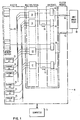
- the apparatus is a tester 10 of which only the tester channels 25 are shown.
- the tests to be performed and the interrogation related to the results of the tests are provided by a general purpose computer 15.
- This computer has a pre-established memory incorporated therewith for purposes of providing a test to the integrated circuit unit under test (UUT) 50.
- the computer in this particular instance, also controls a high-speed memory buffer 20 with as many memory cells or memory positions as there are input/output terminal pins at the UUT 50. Test patterns are stored in this memory buffer, one test sequence at a time.
- Tester channels 25 are assigned to several classes according to a sorting scheme illustrated in Fig. 4. These tester channels, also represented in more detail in Fig. 2, are connected to a plurality of multiplexers 30, 31, ..., 60, 61. Each pair of multiplexers has its inputs connected to a multitude of channels, each of which represents a separate category, with an additional multiplexer input connected to a single independent channel to service an output terminal of the UUT. All inputs to the first multiplexer of each pair have their digital-to-analog converters set at a single level that represents the logic 1 condition of a particular class. Similarly, all inputs to the second multiplexer of each pair have their digital-to-analog converters set at the 0 logic level of that class.
- each input or output terminal there exists a pair of multiplexers, or a single multiplexer, if the schematic diagram of Fig. 3 is used. At any one time, only one of the two multiplexers is operational. If the pattern bit corresponding to the module pin k is a 1, then switching circuit 40 will be ON, whereas switching circuit 41 preceded by a logic NOT circuit 35 will be OFF. Furthermore, the multiplexers of pin k will already have been preset to some defined level, depending on the class input k belongs to. The outputs of multiplexers 30 and 31 are, therefore, at some voltage or current level +L and "":L, respectively, that are characteristic of all inputs of that class. At the tester probe 45, either +L or -L will be present, depending on the bit content of the narticular test pattern.
- Fig. 2 illustrates a tester channel represented in Fig. 1 by channels 25.
- a digital-to-analog converter 100 outputs a level that approximately defines a logic 1. This level +L is set higher than -L which is outputted by digital-to-analog converter 110. The precise value of -L is not relevant.
- the line F1/F0 is the output of a switch that is set in this present example to F1.
- the output of driver 120 is connected to a resistor 130 which in turn, is connected via cable 135 to two solid-state switches 140 and 145, depending whether a 90 ohms or a 750 ohms combination is desired.
- Any voltage above the reference voltage returns a logic 1 at the output of driver 180, whereas a voltage below the reference voltage returns a logic 0.
- This binary level is compared with the expected binary level of the appropriate bit of the test pattern. A logic discrepancy is recorded as an error.
- each test pattern forces either a 0 or 1 to every input pin. Since the voltage levels corresponding to a 0 and a 1 are fixed once the channel assignments have been made for a UUT, whether level -L or +L is selected will depend on the 0/1 bit configuration of the test patterns Those bits will open or close the solid stage switches labeled 40 and 41, (Fig. 3) thus allowing either channel A1,..., or A0, ...., to be connected to the input pin.
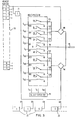
- Fig. 3 illustrates a more detailed view of a sample multiplexer circuit configuration.
- the pair of multiplexers referred to in Fig. 1 is here shown as a single electrical circuit.
- Each input A1, B1, C1 and D1 from the channels 25 represents a different +L level, whereas A0, 80, CO and DO represents the equivalent counter level -L.
- Input 0 is added for the case when the UUT terminal associated with the multiplexer is an output.
- a selector circuit 42 automatically selects which inputs A1,..., D and A0,.. ., DO or 0 are to be connected to the UUT terminal.
- the computer also takes into consideration the loading limitations of each tester channel 25. Further limitations will be described hereinafter. If the terminal is an output, relay output lines 131-134 and 136-139 remain open, whereas 36 is connected. A tester channel will then be uniquely connected to the terminal 45.
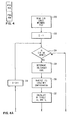
- Fig. 4 illustrates the routine that sorts all input terminals into a plurality of classes. Each class uniquely defines a type and electrical net configuration of the input circuitry tied to the input. Typically, this sorting routine is exercised once per module part number and is run independently from the testing activities.
- a description file of the electrical networks of all input/output pins as shown by block 220 in Fig. 4 is read.
- Each terminal is analyzed, one at a time, to determine first if it is an input or an output (block 224). If it is an output, the name of the pin is stored in a class by itself. All members of this output class will be assigned each their own tester channel. If the terminal is identified as an input, the program interrogates further to ascertain its circuit type or "pin type" (block 228). Further analysis identifies the nature and number of electrical loads and other circuits that are tied to that net (block 230).
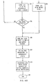
- the levels +L and -L are calculated as a function of the pin type (block 232) and I/O electrical network and stored in their appropriate class (block 234). This process is repeated for each terminal pin (blocks 236 and 238) until all I/O's have been classified.
- the following classes have been populated (block 24): an output class, and a plurality of input categories, subdivided in two sub-classes: a +L level and a -L level sub-class.
- the computer proceeds then to set all digital-to-analog converters to their appropriate levels (block 242), and the select circuitry of each multiplexer is set to assign the channels to the input pins (block 244). After this assignment is completed, the program comes to an end (block 246).
- semiconductor packages that exceed the number of available tester channels may be tested without having to resort to a tester with a higher number of channels.
Landscapes
- Engineering & Computer Science (AREA)
- Computer Networks & Wireless Communication (AREA)
- General Engineering & Computer Science (AREA)
- Physics & Mathematics (AREA)
- General Physics & Mathematics (AREA)
- Tests Of Electronic Circuits (AREA)
Description
- The present invention relates to a method and apparatus for testing electrical circuit units having a plurality of terminals or pins by a tester that lacks the number of necessary channels to connect one circuit pin to one tester channel. More particularly, this invention relates to the utilization of a tester in which the number of terminals of an integrated circuit unit under test exceeds by a substantial margin the number of testing lines that the tester has available to make a connection.
- The practice of testing integrated circuit components is of prime importance to the electronic device manufacturers so as to weed out defective units before they are assembled and used. It is desirable to test semiconductor devices while they are still part of a wafer so as to discover unsatisfactory components prior to being mounted on the next level of packaging. Similarly, it is also desirable to test further these integrated circuit units after that they have been assembled on modules, cards or boards. Only by means of repetitive testing can the quality assurance of the devices be safeguarded. This continuous testing at each level of packaging imposes demands on the electronic industry to design and provide equipment that is capable of performing these tests in an automatic mode, at high speeds and with precise accuracy.
- The trend of the electronic industry developments is to further increase the degree of miniaturization of electronic devices. This implies decreasing the area of each circuit which, in turn, allows for an increase in the density of circuits. A higher circuit count permits more logic functions to be performed by the integrated unit. This trend towards miniaturization is also accompanied by a corresponding increase in the number of terminal pins. This is necessary to maintain adequate communication between the circuitry of the unit and the remainder of the assembly or machine which it is part of.
- As integrated circuits become more sophisticated, the complexity of the supporting test equipment must increase correspondingly. This signifies that the number of tests that must be performed to locate all the faults increases rapidly. For example, on a simple integrated circuit of no more than a dozen circuits, at most, several tens of tests are sufficient to locate all possible failures. In today's integrated circuits, with its hundreds and soon thousands of circuits, the number of tests required is in the order of many tens of thousands to achieve the same result. Not only the software requirements to generate such test patterns are difficult, but the time needed to apply them is inordinately long. A direct consequence of this trend toward miniaturization is that the test equipment must be able to process a large number of patterns at high speed. Such electronic tester is usually controlled by a computer. The tester generates a signal that is provided to the integrated circuit or assembly, hereinafter referred to interchangeably as a unit under test (UUT). This signal which is in the form of a forced voltage or current is supplied to the appropriate input terminal pin by digital-to-analog converter (or D/A converter). This, and other pertinent circuitry forms a "tester channel". As the name states it, it converts a "logic binary level" into an electrical analog level which is applied to a single input terminal of the unit under test (UUT). In a similar fashion, the actual electrical response at the output pins of the UUT is compared to a standard acceptable response by the computer. These responses are dictated by the test patterns. For example, if the expected binary level at one output pin of the UUT is a "
logic 1 ", the tester, by use of the channel connected to that output pin, will measure the voltage or current level. - A nonconcurrence between the measured and expected levels indicates the presence of a failure inside of the integrated circuit, and the unit is discarded as defective.
- Prior approaches to related problems in the testing art are shown in the following.
- U.S. Patent No. 3,848,188 entitled "Multiplexer Control System For A Multi-Array Test Probe Assembly", granted November 12, 1974 to Frank J. Ardezzone et al describes a multiplexer control system for a multi-array test probe assembly for controlling the simultaneous interface contact of the probe arrays with a plurality of electronic devices and the successive interconnection of said arrays with electronic test equipment.
- Another multiplex device is disclosed in U.S. Patent No. 3,922,537, entitled "Multiplex Device For Automatic Test Equipment" granted November 25, 1975 to Phillip C. Jackson. It shows a multiplex apparatus for an automatic computerized diagnostic testing system for selectively interconnecting peripheral measurement and stimulus devices to a unit under test (UUT) through various switching subsystems which differ in switching capability, load carrying ability, frequency bandwidth and mode of operation. The multiplexer includes plural conducting means between each pin of the circuit under test and corresponding terminals or test points of plural switching subsystems used to interconnect UUT pins and the peripheral testing devices. Each plural conducting means includes controllable switch means. These switch means operate automatically under programmed computer control. One of the switching subsystems has high frequency signal carrying ability, and the conducting means associated with this subsystem preferably include impedance matching buffers, and have a frequency bandwidth equal to that of the subsystem.
- Today, a one to one correspondence between each tester channel and a terminal pin of a UUT always exists. By presetting each tester channel to a defined level, it is possible to assign a voltage or current level appropriate to each terminal connection. The prior art, however, does not solve the problem when the tester falls behind the advances in the complexity of the semiconductor technology and when an inadequate number of tester channels is present to service the totality of terminal pins of the UUT. In other words, the prior art does not solve the problem of testing a UUT whose number of terminals exceeds substantially the number of available testing lines or channels.
- Here the invention as claimed intends to provide a remedy. In effect, this invention provides an advance over the prior art by enabling a tester with less channels than those required by the integrated circuit package to actually test this package as if an adequate number of channels were available. In particular, this invention is useful to test large scale integrated packages that represent the latest advances in technology with existing test equipment whose architecture and characteristics have not fully matched the advances in semiconductor technology packages.
- To overcome many of the above-mentioned shortcomings and to provide a practical system to match a large or very large scale integrated circuit package (LSI or VLSI) with terminal pins in excess over the available number of tester channels, the present invention as claimed provides a method and apparatus for connecting a plurality of input terminal pins to a single channel.
- In principle, the invention makes use of a high-speed memory buffer with one memory cell per terminal pin for storing the test pattern sequence to be applied to the UUT and a switching network that permits delivering a voltage or current level to an input terminal. The controlling line that allows the voltage or current to reach the input pin is determined by the test pattern bit that corresponds to that input pin.
- In the illustrative embodiment, the UUT is represented by a multi-chip-module (MCM) with a plurality of input and output terminals. The tester is computer controlled. The number of available tester channels is less than the number of terminals required to test the module. All input pins are classified in a plurality of categories, each of which corresponds to a unique circuit type and electrical network configuration. The object of this sorting process is to single out every possible electrical characteristic that affects the DC levels to be applied during testing of the module. Output terminal pins, on the other hand, are not processed by the aforementioned sorting.
- This invention requires that each bilevel electrical signal pattern to be applied to input terminals and sensed at the output terminals in the package under test to determine whether the package is defective, be stored in a high speed memory buffer, such that there exist a one to one correspondence between a storage position and an input or output of the module under test. This invention requires furthermore that each tester channel be connected to inputs capable of driving a plurality of input pins. All members of this plurality belong to a single category of inputs, that is characterized by a unique circuit type and electrical network configuration. Such input channels are set at a fixed level capable of delivering the appropriate DC voltage to each member of the group of inputs The selection of members of each plurality is determined by the aforementioned sorting process and is implemented in the embodiment by a set of multiplexers. Each multiplexer selects 1 out of n possible DC levels that are appropriate to each input pin.
- Since each functional test pattern consists of a sequence of a logic "0"s and "1"s, there exists one DC level for each state that is appropriate to a plurality of inputs. This invention requires furthermore that each output of the UUT be assigned its own tester channel. This is necessary to allow a comparison between the measured DC level and the expected level as defined by the test pattern. The channel selection for the outputs of the UUT is controlled by the multiplexer that inhibits its other inputs from interfering with the channel selected for connection to that output.
- The theoretical limitation of this invention is testing a complex MCM of k outputs and p input pins divided in m classes, where p»m, (p much larger than m) on a tester of no less than 2m+k channels.
- The testing system of the present invention, as briefly described above, provides an important advantage in that integrated circuit packages whose terminal pins exceed the number of available channels may be tested without having to resort to a tester with a higher number of channels.
- The invention will be more clearly understood by reference to the description below taken in conjunction with the accompanying drawings wherein:
- Fig. 1 is a simplified block diagram of the present invention diagrammatically illustrating the connections between each tester and a plurality of terminals of a module under test.
- Fig. 2 is a detailed electrical schematic of a tester channel to be used as input to the multiplexers of Fig. 3.
- Fig. 3 is a detailed schematic diagram of the switching circuitry according to this invention.
- Fig. 4, a composite of Figures 4A and 4B, is a flow chart of routine that sorts all input terminals into a plurality of classes as a function of the circuit types and electrical nets associated to each terminal pin.
- In order to afford a complete understanding of the invention and an appreciation of its advantages, an embodiment is presented below in the context of a practical environment.
- Referring first to Fig. 1, the apparatus is a
tester 10 of which only thetester channels 25 are shown. The tests to be performed and the interrogation related to the results of the tests, are provided by ageneral purpose computer 15. This computer has a pre-established memory incorporated therewith for purposes of providing a test to the integrated circuit unit under test (UUT) 50. The computer, in this particular instance, also controls a high-speed memory buffer 20 with as many memory cells or memory positions as there are input/output terminal pins at theUUT 50. Test patterns are stored in this memory buffer, one test sequence at a time. -
Tester channels 25 are assigned to several classes according to a sorting scheme illustrated in Fig. 4. These tester channels, also represented in more detail in Fig. 2, are connected to a plurality ofmultiplexers logic 1 condition of a particular class. Similarly, all inputs to the second multiplexer of each pair have their digital-to-analog converters set at the 0 logic level of that class. For each input or output terminal, there exists a pair of multiplexers, or a single multiplexer, if the schematic diagram of Fig. 3 is used. At any one time, only one of the two multiplexers is operational. If the pattern bit corresponding to the module pin k is a 1, then switchingcircuit 40 will be ON, whereas switchingcircuit 41 preceded by alogic NOT circuit 35 will be OFF. Furthermore, the multiplexers of pin k will already have been preset to some defined level, depending on the class input k belongs to. The outputs ofmultiplexers tester probe 45, either +L or -L will be present, depending on the bit content of the narticular test pattern. - Fig. 2 illustrates a tester channel represented in Fig. 1 by
channels 25. A digital-to-analog converter 100 outputs a level that approximately defines alogic 1. This level +L is set higher than -L which is outputted by digital-to-analog converter 110. The precise value of -L is not relevant. The line F1/F0 is the output of a switch that is set in this present example to F1. The output ofdriver 120 is connected to aresistor 130 which in turn, is connected viacable 135 to two solid-state switches point 175, whereas, when it is used as an output, calibration is effected atpoint 125. When the tester channel is used for an output, the reference digital-to-analog converter 115 is set to an appropriate reference level. The combination ofresistors point 125 provides a Theyenin's equivalent resistance and voltage that acts as a load to the UUT output pin. The measured level under the aforementioned loading conditions is compared with the preset reference level. Both inputs todriver 180 are appropriately attenuated by means of theresistor dividers logic 1 at the output ofdriver 180, whereas a voltage below the reference voltage returns alogic 0. This binary level is compared with the expected binary level of the appropriate bit of the test pattern. A logic discrepancy is recorded as an error. - During operation, a plurality of terminal pins is connected to one channel. Each test pattern forces either a 0 or 1 to every input pin. Since the voltage levels corresponding to a 0 and a 1 are fixed once the channel assignments have been made for a UUT, whether level -L or +L is selected will depend on the 0/1 bit configuration of the test patterns Those bits will open or close the solid stage switches labeled 40 and 41, (Fig. 3) thus allowing either channel A1,..., or A0, ...., to be connected to the input pin.
- Fig. 3 illustrates a more detailed view of a sample multiplexer circuit configuration. The pair of multiplexers referred to in Fig. 1 is here shown as a single electrical circuit. Each input A1, B1, C1 and D1 from the
channels 25 represents a different +L level, whereas A0, 80, CO and DO represents the equivalent counter level -L. Input 0 is added for the case when the UUT terminal associated with the multiplexer is an output. Aselector circuit 42 automatically selects which inputs A1,..., D and A0,.. ., DO or 0 are to be connected to the UUT terminal. Thecomputer 15 of Fig. 1 analyzes the input/output terminal configuration, classifies the terminal pins in several classes and assigns a plurality of input terminals to each tester channel by means ofselector circuit 42. The computer also takes into consideration the loading limitations of eachtester channel 25. Further limitations will be described hereinafter. If the terminal is an output, relay output lines 131-134 and 136-139 remain open, whereas 36 is connected. A tester channel will then be uniquely connected to the terminal 45. - Fig. 4 illustrates the routine that sorts all input terminals into a plurality of classes. Each class uniquely defines a type and electrical net configuration of the input circuitry tied to the input. Typically, this sorting routine is exercised once per module part number and is run independently from the testing activities.
- In the embodiment of the invention illustrated in the drawings, a description file of the electrical networks of all input/output pins as shown by
block 220 in Fig. 4 is read. Each terminal is analyzed, one at a time, to determine first if it is an input or an output (block 224). If it is an output, the name of the pin is stored in a class by itself. All members of this output class will be assigned each their own tester channel. If the terminal is identified as an input, the program interrogates further to ascertain its circuit type or "pin type" (block 228). Further analysis identifies the nature and number of electrical loads and other circuits that are tied to that net (block 230). Finally, the levels +L and -L are calculated as a function of the pin type (block 232) and I/O electrical network and stored in their appropriate class (block 234). This process is repeated for each terminal pin (blocks 236 and 238) until all I/O's have been classified. Upon completion of this iterative process, the following classes have been populated (block 24): an output class, and a plurality of input categories, subdivided in two sub-classes: a +L level and a -L level sub-class. The computer proceeds then to set all digital-to-analog converters to their appropriate levels (block 242), and the select circuitry of each multiplexer is set to assign the channels to the input pins (block 244). After this assignment is completed, the program comes to an end (block 246). - The limitation of the method described in this invention was briefly mentioned above. A module part number of k outputs, p inputs divided into m classes, where p»m, (p very much larger than m) requires a tester of at least 2m+k channels. Of these 2m, m are assigned to the +L levels and m to -L. There exists, furthermore, another limitation that relates to loading down a tester channel when too many input terminals are connected to it. Under such circumstances, it becomes unfeasible for a channel to deliver the expected voltage to all the terminals it is connected to. This limitation is not a severe constraint, because several channels may usually be assigned to each particular class of inputs.
- A statistical analysis of various technologies has shown that there exists a limited set of "0" and "1" DC levels that are to be applied to inputs of the unit under test, perhaps as few as 6 and as many as 15. Such statistical analysis forms no part of our invention.
- With this information, semiconductor packages that exceed the number of available tester channels may be tested without having to resort to a tester with a higher number of channels.
Claims (8)
Applications Claiming Priority (2)
| Application Number | Priority Date | Filing Date | Title |
|---|---|---|---|
| US06/104,481 US4348759A (en) | 1979-12-17 | 1979-12-17 | Automatic testing of complex semiconductor components with test equipment having less channels than those required by the component under test |
| US104481 | 1979-12-17 |
Publications (2)
| Publication Number | Publication Date |
|---|---|
| EP0030723A1 EP0030723A1 (en) | 1981-06-24 |
| EP0030723B1 true EP0030723B1 (en) | 1983-10-05 |
Family
ID=22300730
Family Applications (1)
| Application Number | Title | Priority Date | Filing Date |
|---|---|---|---|
| EP80107860A Expired EP0030723B1 (en) | 1979-12-17 | 1980-12-12 | Method and apparatus for the automatic testing of semi-conductor components |
Country Status (4)
| Country | Link |
|---|---|
| US (1) | US4348759A (en) |
| EP (1) | EP0030723B1 (en) |
| JP (1) | JPS5687874A (en) |
| DE (1) | DE3065212D1 (en) |
Cited By (1)
| Publication number | Priority date | Publication date | Assignee | Title |
|---|---|---|---|---|
| DE3509247A1 (en) * | 1984-03-14 | 1985-11-21 | Teradyne Inc., Boston, Mass. | RELAY MULTIPLEX CIRCUIT FOR TESTING CIRCUITS |
Families Citing this family (52)
| Publication number | Priority date | Publication date | Assignee | Title |
|---|---|---|---|---|
| US4439858A (en) * | 1981-05-28 | 1984-03-27 | Zehntel, Inc. | Digital in-circuit tester |
| US4397021A (en) * | 1981-06-15 | 1983-08-02 | Westinghouse Electric Corp. | Multi-processor automatic test system |
| US4517661A (en) * | 1981-07-16 | 1985-05-14 | International Business Machines Corporation | Programmable chip tester having plural pin unit buffers which each store sufficient test data for independent operations by each pin unit |
| US4503386A (en) * | 1982-04-20 | 1985-03-05 | International Business Machines Corporation | Chip partitioning aid (CPA)-A structure for test pattern generation for large logic networks |
| US4570262A (en) * | 1983-06-22 | 1986-02-11 | The Boeing Company | Programmable universal logic driver |
| JPS60158527A (en) * | 1984-01-27 | 1985-08-19 | 横河・ヒユ−レツト・パツカ−ド株式会社 | Method of driving relay |
| US4604744A (en) * | 1984-10-01 | 1986-08-05 | Motorola Inc. | Automated circuit tester |
| US4644265A (en) * | 1985-09-03 | 1987-02-17 | International Business Machines Corporation | Noise reduction during testing of integrated circuit chips |
| US4931723A (en) * | 1985-12-18 | 1990-06-05 | Schlumberger Technologies, Inc. | Automatic test system having a "true tester-per-pin" architecture |
| US4744084A (en) * | 1986-02-27 | 1988-05-10 | Mentor Graphics Corporation | Hardware modeling system and method for simulating portions of electrical circuits |
| US4862067A (en) * | 1987-06-24 | 1989-08-29 | Schlumberger Technologies, Inc. | Method and apparatus for in-circuit testing of electronic devices |
| US4908576A (en) * | 1987-09-08 | 1990-03-13 | Jackson Daniel K | System for printed circuit board testing |
| US4858208A (en) * | 1988-07-11 | 1989-08-15 | Motorola, Inc. | Apparatus and method for testing semiconductor devices |
| US4972413A (en) * | 1989-03-23 | 1990-11-20 | Motorola, Inc. | Method and apparatus for high speed integrated circuit testing |
| US4989209A (en) * | 1989-03-24 | 1991-01-29 | Motorola, Inc. | Method and apparatus for testing high pin count integrated circuits |
| US5010297A (en) * | 1989-12-01 | 1991-04-23 | Analog Devices, Incorporated | Automatic test equipment with active load having high-speed inhibit mode switching |
| JPH03194800A (en) * | 1989-12-25 | 1991-08-26 | Ando Electric Co Ltd | Real time address switching circuit |
| US5131272A (en) * | 1990-03-15 | 1992-07-21 | Harris Corporation | Portable deployable automatic test system |
| JP2513904B2 (en) * | 1990-06-12 | 1996-07-10 | 株式会社東芝 | Testability circuit |
| JP2956913B2 (en) * | 1991-05-15 | 1999-10-04 | 株式会社アドバンテスト | IC test equipment |
| JP3377225B2 (en) * | 1992-04-07 | 2003-02-17 | 富士写真フイルム株式会社 | Integrated circuit including check circuit |
| US5550844A (en) * | 1992-11-19 | 1996-08-27 | Proteus Corporation | Printed circuit board fault injection circuit |
| JPH0720208A (en) * | 1993-07-02 | 1995-01-24 | Mitsubishi Electric Corp | Test method and test system for device under test |
| US5604750A (en) * | 1994-11-01 | 1997-02-18 | Vlsi Technology, Inc. | Method for voltage setup of integrated circuit tester |
| US5778004A (en) * | 1995-06-02 | 1998-07-07 | Unisys Corporation | Vector translator |
| US5608337A (en) * | 1995-06-07 | 1997-03-04 | Altera Corporation | Method and apparatus of testing an integrated circuit device |
| EP0882239B1 (en) * | 1996-02-06 | 2009-06-03 | Telefonaktiebolaget LM Ericsson (publ) | Assembly and method for testing integrated circuit devices |
| FR2751082B1 (en) * | 1996-07-10 | 1998-11-06 | Aerospatiale | SWITCHING DEVICE, IN PARTICULAR FOR A SYSTEM UNDER TEST |
| JPH10319095A (en) * | 1997-05-22 | 1998-12-04 | Mitsubishi Electric Corp | Semiconductor test equipment |
| US6260163B1 (en) | 1997-12-12 | 2001-07-10 | International Business Machines Corporation | Testing high I/O integrated circuits on a low I/O tester |
| US6201383B1 (en) | 1998-01-22 | 2001-03-13 | International Business Machines Corporation | Method and apparatus for determining short circuit conditions using a gang probe circuit tester |
| US6131172A (en) * | 1998-02-20 | 2000-10-10 | Micron Electronics, Inc. | Method for classifying electronic devices |
| US6104985A (en) * | 1998-02-20 | 2000-08-15 | Micron Electronics, Inc. | Device for classifying electronic components |
| US6032107A (en) * | 1998-05-19 | 2000-02-29 | Micron Technology, Inc. | Calibrating test equipment |
| US6170071B1 (en) * | 1998-07-27 | 2001-01-02 | Lucent Technologies, Inc. | Method for optimizing test fixtures to minimize vector load time for automated test equipment |
| US6385740B1 (en) * | 1998-08-21 | 2002-05-07 | Advanced Micro Devices, Inc. | Method to dynamically change microprocessor test software to reflect different silicon revision levels |
| US6430705B1 (en) * | 1998-08-21 | 2002-08-06 | Advanced Micro Devices, Inc. | Method for utilizing virtual hardware descriptions to allow for multi-processor debugging in environments using varying processor revision levels |
| US6374379B1 (en) * | 1999-02-05 | 2002-04-16 | Teradyne, Inc. | Low-cost configuration for monitoring and controlling parametric measurement units in automatic test equipment |
| US6590644B1 (en) * | 2001-01-12 | 2003-07-08 | Ciena Corporation | Optical module calibration system |
| US6700396B1 (en) * | 2001-05-16 | 2004-03-02 | Ltx Corporation | Integrated micromachine relay for automated test equipment applications |
| US6735543B2 (en) * | 2001-11-29 | 2004-05-11 | International Business Machines Corporation | Method and apparatus for testing, characterizing and tuning a chip interface |
| US6971045B1 (en) | 2002-05-20 | 2005-11-29 | Cyress Semiconductor Corp. | Reducing tester channels for high pinout integrated circuits |
| US6885212B2 (en) | 2002-06-25 | 2005-04-26 | Fujitsu Limited | Semiconductor device and test method for the same |
| US7028896B2 (en) * | 2002-08-22 | 2006-04-18 | Arthur Blank & Company, Inc. | Transaction card fabrication control system and method |
| US7010733B2 (en) * | 2002-10-09 | 2006-03-07 | International Business Machines Corporation | Parametric testing for high pin count ASIC |
| KR100512175B1 (en) * | 2003-03-17 | 2005-09-02 | 삼성전자주식회사 | Semiconductor integrated circuit capable of selecting output signals and method for testing thereof |
| US20040199838A1 (en) * | 2003-03-19 | 2004-10-07 | Rutkowski Paul William | Enhanced boundary-scan method and apparatus providing tester channel reduction |
| US7024330B2 (en) * | 2003-03-28 | 2006-04-04 | Mitsubishi Electric And Electronics U.S.A., Inc. | Method and apparatus for decreasing automatic test equipment setup time |
| US7649366B2 (en) * | 2006-09-01 | 2010-01-19 | Formfactor, Inc. | Method and apparatus for switching tester resources |
| US7576550B2 (en) * | 2007-03-30 | 2009-08-18 | Qualitau, Inc. | Automatic multiplexing system for automated wafer testing |
| JP4437508B1 (en) * | 2009-02-27 | 2010-03-24 | 株式会社アドバンテスト | Test equipment |
| US11555828B2 (en) * | 2020-07-07 | 2023-01-17 | Micron Technology, Inc. | Testing probe system for testing semiconductor die, multi-channel die having shared pads, and related systems and methods |
Citations (2)
| Publication number | Priority date | Publication date | Assignee | Title |
|---|---|---|---|---|
| US3927371A (en) * | 1974-02-19 | 1975-12-16 | Ibm | Test system for large scale integrated circuits |
| GB2020439A (en) * | 1978-05-05 | 1979-11-14 | Zehntel Inc | Circuit digital tester |
Family Cites Families (11)
| Publication number | Priority date | Publication date | Assignee | Title |
|---|---|---|---|---|
| US4055801A (en) * | 1970-08-18 | 1977-10-25 | Pike Harold L | Automatic electronic test equipment and method |
| US3848188A (en) * | 1973-09-10 | 1974-11-12 | Probe Rite Inc | Multiplexer control system for a multi-array test probe assembly |
| US4097797A (en) * | 1974-10-17 | 1978-06-27 | Burroughs Corporation | Apparatus for testing electrical circuit units such as printed circuit cards |
| US3976940A (en) * | 1975-02-25 | 1976-08-24 | Fairchild Camera And Instrument Corporation | Testing circuit |
| US4023097A (en) * | 1975-11-21 | 1977-05-10 | Datatron, Inc. | Noise and dielectric absorption compensation circuit |
| US4034287A (en) * | 1975-12-15 | 1977-07-05 | Pitney-Bowes, Inc. | General purpose digital logic monitor |
| US4044244A (en) * | 1976-08-06 | 1977-08-23 | International Business Machines Corporation | Automatic tester for complex semiconductor components including combinations of logic, memory and analog devices and processes of testing thereof |
| US4070565A (en) * | 1976-08-18 | 1978-01-24 | Zehntel, Inc. | Programmable tester method and apparatus |
| US4195258A (en) * | 1977-03-01 | 1980-03-25 | Intel Corporation | Logic analyzer for integrated circuits, microcomputers, and the like |
| US4092589A (en) * | 1977-03-23 | 1978-05-30 | Fairchild Camera And Instrument Corp. | High-speed testing circuit |
| US4155118A (en) * | 1977-09-20 | 1979-05-15 | Burroughs Corporation | Organization for an integrated circuit calculator/controller |
-
1979
- 1979-12-17 US US06/104,481 patent/US4348759A/en not_active Expired - Lifetime
-
1980
- 1980-09-12 JP JP12619280A patent/JPS5687874A/en active Pending
- 1980-12-12 EP EP80107860A patent/EP0030723B1/en not_active Expired
- 1980-12-12 DE DE8080107860T patent/DE3065212D1/en not_active Expired
Patent Citations (2)
| Publication number | Priority date | Publication date | Assignee | Title |
|---|---|---|---|---|
| US3927371A (en) * | 1974-02-19 | 1975-12-16 | Ibm | Test system for large scale integrated circuits |
| GB2020439A (en) * | 1978-05-05 | 1979-11-14 | Zehntel Inc | Circuit digital tester |
Cited By (1)
| Publication number | Priority date | Publication date | Assignee | Title |
|---|---|---|---|---|
| DE3509247A1 (en) * | 1984-03-14 | 1985-11-21 | Teradyne Inc., Boston, Mass. | RELAY MULTIPLEX CIRCUIT FOR TESTING CIRCUITS |
Also Published As
| Publication number | Publication date |
|---|---|
| JPS5687874A (en) | 1981-07-16 |
| US4348759A (en) | 1982-09-07 |
| EP0030723A1 (en) | 1981-06-24 |
| DE3065212D1 (en) | 1983-11-10 |
Similar Documents
| Publication | Publication Date | Title |
|---|---|---|
| EP0030723A1 (en) | Method and apparatus for the automatic testing of semi-conductor components | |
| US4044244A (en) | Automatic tester for complex semiconductor components including combinations of logic, memory and analog devices and processes of testing thereof | |
| EP0388790B1 (en) | Method and apparatus for testing high pin count integrated circuits | |
| US3922537A (en) | Multiplex device for automatic test equipment | |
| EP0108790B1 (en) | Integrated circuit test apparatus | |
| US5736850A (en) | Configurable probe card for automatic test equipment | |
| US7245139B2 (en) | Tester channel to multiple IC terminals | |
| US4439858A (en) | Digital in-circuit tester | |
| US6195772B1 (en) | Electronic circuit testing methods and apparatus | |
| US7486095B2 (en) | System for measuring signal path resistance for an integrated circuit tester interconnect structure | |
| EP0549602B1 (en) | Integrated circuit, system and method for fault insertion | |
| US5861743A (en) | Hybrid scanner for use in an improved MDA tester | |
| CA2245549C (en) | Assembly and method for testing integrated circuit devices | |
| US4180203A (en) | Programmable test point selector circuit | |
| JPH0783988A (en) | Circuit-board testing device | |
| US5712858A (en) | Test methodology for exceeding tester pin count for an asic device | |
| CN109633417B (en) | Multi-chip simultaneous testing structure and method | |
| US5043655A (en) | Current sensing buffer for digital signal line testing | |
| WO1988007204A1 (en) | Tri-state circuit tester | |
| CN113960456B (en) | Automatic detection method for micro-damage of circuit interface | |
| EP0145194B1 (en) | Automatic test equipment | |
| JPH11148964A (en) | Integrated circuit testing device and method | |
| US7010733B2 (en) | Parametric testing for high pin count ASIC | |
| JPS5882346A (en) | Automatic correction for pin electronics interface circuit within electronic tester | |
| JPH11311661A (en) | Semiconductor device-testing system and method therefor |
Legal Events
| Date | Code | Title | Description |
|---|---|---|---|
| PUAI | Public reference made under article 153(3) epc to a published international application that has entered the european phase |
Free format text: ORIGINAL CODE: 0009012 |
|
| AK | Designated contracting states |
Designated state(s): DE FR GB IT |
|
| 17P | Request for examination filed |
Effective date: 19810706 |
|
| GRAA | (expected) grant |
Free format text: ORIGINAL CODE: 0009210 |
|
| AK | Designated contracting states |
Designated state(s): DE FR GB IT |
|
| PG25 | Lapsed in a contracting state [announced via postgrant information from national office to epo] |
Ref country code: IT Free format text: LAPSE BECAUSE OF FAILURE TO SUBMIT A TRANSLATION OF THE DESCRIPTION OR TO PAY THE FEE WITHIN THE PRESCRIBED TIME-LIMIT;WARNING: LAPSES OF ITALIAN PATENTS WITH EFFECTIVE DATE BEFORE 2007 MAY HAVE OCCURRED AT ANY TIME BEFORE 2007. THE CORRECT EFFECTIVE DATE MAY BE DIFFERENT FROM THE ONE RECORDED. Effective date: 19831005 |
|
| REF | Corresponds to: |
Ref document number: 3065212 Country of ref document: DE Date of ref document: 19831110 |
|
| ET | Fr: translation filed | ||
| PLBE | No opposition filed within time limit |
Free format text: ORIGINAL CODE: 0009261 |
|
| STAA | Information on the status of an ep patent application or granted ep patent |
Free format text: STATUS: NO OPPOSITION FILED WITHIN TIME LIMIT |
|
| 26N | No opposition filed | ||
| PGFP | Annual fee paid to national office [announced via postgrant information from national office to epo] |
Ref country code: GB Payment date: 19901119 Year of fee payment: 11 |
|
| PGFP | Annual fee paid to national office [announced via postgrant information from national office to epo] |
Ref country code: FR Payment date: 19901122 Year of fee payment: 11 |
|
| PGFP | Annual fee paid to national office [announced via postgrant information from national office to epo] |
Ref country code: DE Payment date: 19901231 Year of fee payment: 11 |
|
| PG25 | Lapsed in a contracting state [announced via postgrant information from national office to epo] |
Ref country code: GB Effective date: 19911212 |
|
| GBPC | Gb: european patent ceased through non-payment of renewal fee | ||
| PG25 | Lapsed in a contracting state [announced via postgrant information from national office to epo] |
Ref country code: FR Effective date: 19920831 |
|
| PG25 | Lapsed in a contracting state [announced via postgrant information from national office to epo] |
Ref country code: DE Effective date: 19920901 |
|
| REG | Reference to a national code |
Ref country code: FR Ref legal event code: ST |