EP0030347A2 - Electron beam exposure system and apparatus for carrying out the same - Google Patents
Electron beam exposure system and apparatus for carrying out the same Download PDFInfo
- Publication number
- EP0030347A2 EP0030347A2 EP80107513A EP80107513A EP0030347A2 EP 0030347 A2 EP0030347 A2 EP 0030347A2 EP 80107513 A EP80107513 A EP 80107513A EP 80107513 A EP80107513 A EP 80107513A EP 0030347 A2 EP0030347 A2 EP 0030347A2
- Authority
- EP
- European Patent Office
- Prior art keywords
- electron beam
- deflection
- stage
- astigmatism
- correction
- Prior art date
- Legal status (The legal status is an assumption and is not a legal conclusion. Google has not performed a legal analysis and makes no representation as to the accuracy of the status listed.)
- Granted
Links
Images


Classifications
-
- H—ELECTRICITY
- H01—ELECTRIC ELEMENTS
- H01J—ELECTRIC DISCHARGE TUBES OR DISCHARGE LAMPS
- H01J37/00—Discharge tubes with provision for introducing objects or material to be exposed to the discharge, e.g. for the purpose of examination or processing thereof
- H01J37/30—Electron-beam or ion-beam tubes for localised treatment of objects
- H01J37/302—Controlling tubes by external information, e.g. programme control
-
- H—ELECTRICITY
- H01—ELECTRIC ELEMENTS
- H01J—ELECTRIC DISCHARGE TUBES OR DISCHARGE LAMPS
- H01J37/00—Discharge tubes with provision for introducing objects or material to be exposed to the discharge, e.g. for the purpose of examination or processing thereof
- H01J37/02—Details
- H01J37/04—Arrangements of electrodes and associated parts for generating or controlling the discharge, e.g. electron-optical arrangement, ion-optical arrangement
- H01J37/147—Arrangements for directing or deflecting the discharge along a desired path
- H01J37/1472—Deflecting along given lines
- H01J37/1474—Scanning means
- H01J37/1475—Scanning means magnetic
-
- H—ELECTRICITY
- H01—ELECTRIC ELEMENTS
- H01J—ELECTRIC DISCHARGE TUBES OR DISCHARGE LAMPS
- H01J37/00—Discharge tubes with provision for introducing objects or material to be exposed to the discharge, e.g. for the purpose of examination or processing thereof
- H01J37/02—Details
- H01J37/04—Arrangements of electrodes and associated parts for generating or controlling the discharge, e.g. electron-optical arrangement, ion-optical arrangement
- H01J37/153—Electron-optical or ion-optical arrangements for the correction of image defects, e.g. stigmators
-
- H—ELECTRICITY
- H01—ELECTRIC ELEMENTS
- H01J—ELECTRIC DISCHARGE TUBES OR DISCHARGE LAMPS
- H01J37/00—Discharge tubes with provision for introducing objects or material to be exposed to the discharge, e.g. for the purpose of examination or processing thereof
- H01J37/30—Electron-beam or ion-beam tubes for localised treatment of objects
- H01J37/304—Controlling tubes by information coming from the objects or from the beam, e.g. correction signals
Definitions
- the present invention relates to an electron beam exposure system, in which an electron beam is radiated to a medium placed on a continuously moving stage, and an apparatus for exposing a medium by continuously moving the stage supporting said medium.
- the electron beam exposure system is well known as a method for forming minute patterns of an LSI (Large Scale Integrated Circuit).
- This electron beam exposure system is classified into the step and repeat system where patterns are depicted on the wafer by repeating a process that a wafer is exposed to, for example, the variable rectangular beam, then shifted by one step and then exposed to said beam by shifting the stage mounting said wafers step by step, and the continuous stage moving system where patterns are depicted by projecting the beam to the wafers while said stage is always moved continuously.
- the electron beam deflection range is comparatively as wide as 2(two) to 5(five) mm square, and the stage moves 2 to 5 mm in a direction and stops to project the electron beam on a wafer and then moves 2 to 5 mm after the projection.
- the exposed portions are thus sequentially formed by repeating such operations.
- the stage moves continuously at a rate of about 20mm/sec, the beam is scanned in the range as narrow as about 250 um at a right angle to the moving direction of the wafer, and thereby patterns are depicted on the wafers.
- the former step and repeat system has such a merit that the beam position control is easy at the time of depicting patterns since the stage is in the stationary condition, but also has such a demerit that compensation for obscurity such as distortion, field curvature, astigmatism etc. is required since the deflection width of electron beam is wide and the movement of stage lacks smoothness because it is moved step by step for every pattern depiction and always subjected to acceleration and deceleration.
- the latter continuous stage moving system has such a merit that the stage moves smoothly and naturally on account of the continuous movement of the stage and variety of compensations mentioned above are not required due to narrow deflection of the electron beam, but also has such a demerit that the beam position control is complicated due to the continuous movement of stage, a narrow deflection of electron beam provides less amount of exposing process, and thereby a longer period is required for depicting desired patterns.
- an electron beam exposure system in which an electron beam is radiated to a medium mounted on a continuously moving stage characterized in that a correction memory is provided for storing electron beam correction data for a least one of a field curvature, an astigmatism and a distortion which change in accordance with deflection amount of electron beam wherein said deflection amount is obtained from a difference between a medium position data and a beam deflection position data from a processor, and said electron beam correction data corresponding to said deflection amount is read out from said correction memory and applied to a beam control means.
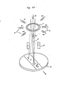
- FIG. 1 and Figure 2 respectively show the embodiment of the electron beam exposure apparatus of the present invention.
- G is an electron gun and B is the electron beam emitted from said electron gun.
- 1 is a first slit for the electron beam B.
- 2 designates deflection plates for deflecting the electron beam section into a variable rectangular shape, 3 a second slit, 4 electron lenses for focusing and image forming and 5 deflection plates for correcting distortion.
- 6 is a stigmator coil
- 7 is a focus coil
- 8 is a deflection coil
- 9 is a convergence coil
- 10 is a medium such as a wafer placed on a stage 11 which moves continuously.
- the electron beam B emitted from the electron gun G is converged by the electron lens 4 whereby an image of the first slit 1 is formed on the second slit 3 and deflected by the deflection plate 2.
- the portion Ba indicated by the mesh of Fig. 3 of the electron beam B passes the aperture 3a of the second slit 3 and shaped into the rectangular beam, and projected to the desired position on the wafer 10 via the electron lens, convergence coil and deflection coil etc.
- the semiconductor wafer 10 allows, as indicated in Fig. 4, formation of many integrated circuit chips 10a, 10b,.... (these are scribed into individual IC chips) and usually respective chips have the same patterns, namely the same internal element arrangement.
- each pattern of the integrated circuit chip is depicted by the procedures indicated in Fig. 5, namely a desired pattern is depicted in unit of individual rectangular patterns B1, B2, B3, across and by adequately combining them, namely the exposing of the photoresist is performed.
- the exposing location on the wafer is shifted in the present invention by the movement of stage 11 and beam deflection by the deflection coil 8.
- a computer.12 used for such control. 13 is a memory for storing pattern data of said integrated circuit chips.
- 14 is a register which stores data of the field coordinates of the chips on the wafer;
- 15 is an adder for adding a readout signal S 1 from the memory 13 and the signal S 2 which means the field coordinate 14 and thereby outputs a combined signal S 3 ;
- 16 is a dynamic correction memory which stores correction data for correcting the field curvature, the astigmatism and the distortion of the electron beam.
- the field coordinates are represented by the specific points of chips on the wafer, for example, by the coordinates of the points P1, P2,.... and the signal S 3 obtained by adding such field coordinate signal and the output signal S1 of the memory 13 indicated the coordinates of individual IC patterns on the wafer.
- the stage 11 is driven in the X and Y directions by a motor, not illustrated, and the locations of X and Y, more specifically., the locations of the field coordinates X, Y of wafer on said stage are measured by the laser interferometer 17.
- the wafer 10 is not always placed on the stage 11 in the determined condition and usually it is deviated or rotated by a certain angle to the X and Y directions from the determined condition.
- 18 is a primary converter consisting of the matrix circuit (which performs addition/subtraction and multipli- cation/division) in order to correct such positional deviation.
- positions of three marks determining the plane of wafer are detected by the electron beams, deviation from the determined position is detected by measuring such positions, an output of the laser interferometer 17 is corrected in accordance with such deviation and said output is set to the coordinates predetermined by the memory 13 and the register 14.
- 19 is a subtractor which outputs a difference signal S 6 obtained by subtracting the signal S 5 of the converter 18 from the signal S 3 of said adder 15.
- the output signal S 6 of the subtractor 19 is added to the amplifier 24 via the primary converter 18.
- the amplifier 24 converts the digital signal S 6 to the analog signal S10 and amplifies said signal in order to excite the deflection coil 8.
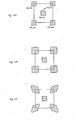
- the pattern is actually not only obscured but also deformed as the electron beam is deflected as indicated in Fig. 6C. This is called the astigmatism.
- the correct pattern can be depicted as indicated in Fig. 6A by correcting astigmatism for the pattern of Fig. 6C to the pattern of Fig. 6B and by correcting the field curvature.
- the pattern is depicted at the correct position like the patterns P 1 , P 2 , P 3 , P 4 on the diagonal of the square with the center P O .
- the pattern P O of the position (x m , y O ) namely even when the information to deflect the pattern P 0 to the position (x m , y O ) is input to the column from the CPU, the electron beam is actually deflected to the position (x , y O ) and the pattern P O is depicted.
- Such deviation of the deflection position is called the distortion.
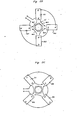
- the focus coil 7 used for correcting the abovementioned field curvature is a ringshape coil wound in such a way as surrounding the electron beam B as indicated in Fig. 2A.
- the stigmator coil 6 used for correcting astigmatism consists of eight (8) solenoid coils a 1 ,... .,a4 and b 1 ,...., b 4 which are arranged in the same plane with an interval of 45 degrees.
- FIGS 2B, 2C show the coils in the form of block and also indicate mutual connections.
- the coils a 1 ,...., a 4 have the same number of turns, but are connected in series so that the backward winding appears in every another coil. Therefore, when a current is applied to each coil via the winding, the pole N appears in the space side surrounded by the coils in the case of coils a 1 and a 3 , and the pole S appears in the case of the coil a 2 and a4. Thereby, as indicated in the figure, the magnetic lines of force m 1 , m 2 , m 31 m 4 appear.
- the circular beam Ci can be deformed vertically or horizontally as indicated by the dotted line by controlling a current flowing through the coils.
- the ellipse beam indicated by the dotted line can be shaped to the circular beam C.
- the coils b 1 ,....,b 4 indicated in Fig. 2C have the same structure as the coils a 1 ,....,a 4 indicated in Fig. 2B and they are arranged with displacement of only 45 degrees.
- the electron beam can be shaped into the direction displaced only by 45 degrees from that in the Fig. 2B.
- the electron beam can be shaped freely by arranging the coils of Fig. 2B, 2C through the combination as indicated in Fig. 2A.
- distortion changes depending on the deflection angle, but is also influenced by the correction of the field curvature and the astigmatism. Therefore, distortion can be understood as the function of beam deflection angle ⁇ and said field curvature and astigmatism.
- correction data of said values for respective deflection angles are written into the memory 16. 21 to 23 are amplifiers for activating the deflection plates 5, stigmator coil 6, focus coil 7 through DA conversion of the output of said memory.
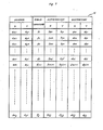
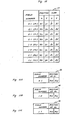
- Figure 7 shows content of the memory 16.
- the one region to be exposed by the electron beam is divided into j sections in the direction X and i sections in the direction Y (i, j are integers).
- the region to be exposed can be considered as the minute regions divided having the addresses from (ax 1 , aY 1 )to(axj, ayi).
- the correction amount of the field curvature at the address (ax 1 , ay 1 ) is pre-obtained as f 1
- correction amount of the astigmatism in the direction X as Sx 1 and that in the direction Y as Sy l is obtained previous to the exposure in the same way, and moreover each correction amount is stored in the memory 16.
- This address corresponds to the deflection amount of the electron beam as will be explained later.
- Figure 8 shows the plan view of the wafer 10 placed on the stage 11.
- the mirrors 81, 82 are respectively provided at the sides in the directions of X and Y of the stage 11, and the laser interferometer 17X for detecting the position in the direction X of the stage 11 and the laser interferometer 17Y for detecting the position in the direction Y of the stage 11 are provided.
- the stage 11 is continuously moved in the directions X and Y with a motor not illustrated, and thereby the region on the wafer 10 is sequentially and continuously exposed as a result of relative operations as indicated by the arrow 83.
- Figure 9 shows an enlarged portion of the wafer 10.
- the chips in size of lx x ly are arranged in the form of matrix on the wafer 10 and the one chip consists of the three exposing fields F 1 , F 2 and F 3 , each is in size of 1 x x l f .
- the size of 1 is a little smaller than the deflection width of electron beam.
- the patterns Q 1 , Q 2 , Q 3 , Q 4 are to be exposed, while Q 5 and Q 6 in the field F 2 , and Q 7 and Q 8 in the field F 3 are to be exposed.
- the origins of the fields F 1 , F 2 and F 3 are respectively indicated by O 1 , 0 2 and 0 3 .
- the coordinate of origin of each field is transferred to the register 14 from the CPU 12 in accordance 'with the fields F 1 , F 2 , F 3 and stored therein.
- the data x 1 , y 1 and 1 1 and 1 1 are read out from the pattern memory 13, while the data O 1x , O 1y are obtained from the register 14. Then, these are added in the adder 15. Thereby, the deflection amount from the origin of exposure by means of the electron beam can be obtained, if the stage is not moved.
- the output signal S 3 in Fig. 1 indicates the coordinates of pattern in the relevant chip (the chip specified by the field coordinate 14 - viewed from the field coordinate of eht wafer 10.
- the laser interferometer 17 provides the current position signal S4 of the wafer 10.
- the signal is substracted from the signal S 3 by the subtractor 19, the difference output signal of the subtractor 19 ist corrected by the primary converter 18, and the output S 6 indicates the amount of deflection of electron beam.
- the deflection coil 8 is activated in accordance with such signal S 6 and therefore the beam is projected to the desired position in accordance with the data of pattern coordinate.
- the stage moves but since the rectangular beam projection period is very short, the wafer is considered to be in the stationary condition during projection of electron beam.
- the difference signal S 6 is also used for retrieval of memory 16, and the correction amount f, S , S , d x , d y of the field curva- ture, astigmatism and distortion corresponding to the deflection amount of the electron beam are read out and then applied to the respective adjusting means 5, 6, 7 via the amplifiers 21 to 23.
- the deflection amounts X, Y are obtained by the following equation.
- (x 1 , y 1 ) is the coordinate of the pattern Q 1 from the origin 0 1
- (X p , Y ) is the coordinate of the origin 0 1
- (X(t), Y(t)) is the output of the laser interferometer, namely the positional coordinate of the stage.
- Above primary conversion is carried out by the primary converter 18 of Figure 1.
- the electron beam exposure system and the apparatus for the same have offered a variety of effects such as a high speed formation of pattern and accurate depiction of patterns since the stage is moved continuously and the rectangular electron beam is projected with deflection by a large deflection angle.
Abstract
Description
- The present invention relates to an electron beam exposure system, in which an electron beam is radiated to a medium placed on a continuously moving stage, and an apparatus for exposing a medium by continuously moving the stage supporting said medium.
- The electron beam exposure system is well known as a method for forming minute patterns of an LSI (Large Scale Integrated Circuit). This electron beam exposure system is classified into the step and repeat system where patterns are depicted on the wafer by repeating a process that a wafer is exposed to, for example, the variable rectangular beam, then shifted by one step and then exposed to said beam by shifting the stage mounting said wafers step by step, and the continuous stage moving system where patterns are depicted by projecting the beam to the wafers while said stage is always moved continuously.
- In the former system, the electron beam deflection range is comparatively as wide as 2(two) to 5(five) mm square, and the stage moves 2 to 5 mm in a direction and stops to project the electron beam on a wafer and then moves 2 to 5 mm after the projection. The exposed portions are thus sequentially formed by repeating such operations. In the latter system, the stage moves continuously at a rate of about 20mm/sec, the beam is scanned in the range as narrow as about 250 um at a right angle to the moving direction of the wafer, and thereby patterns are depicted on the wafers.
- The former step and repeat system has such a merit that the beam position control is easy at the time of depicting patterns since the stage is in the stationary condition, but also has such a demerit that compensation for obscurity such as distortion, field curvature, astigmatism etc. is required since the deflection width of electron beam is wide and the movement of stage lacks smoothness because it is moved step by step for every pattern depiction and always subjected to acceleration and deceleration. On the other hand, the latter continuous stage moving system has such a merit that the stage moves smoothly and naturally on account of the continuous movement of the stage and variety of compensations mentioned above are not required due to narrow deflection of the electron beam, but also has such a demerit that the beam position control is complicated due to the continuous movement of stage, a narrow deflection of electron beam provides less amount of exposing process, and thereby a longer period is required for depicting desired patterns.
- It is an object of the present invention to provide a highly accurate and high speed electron beam exposing system having the merits of both step and repeat system and the continuous stage stifting system outlined above.
- It ist another object of the present invention to provide an apparatus for the high speed electron beam exposure.
- According to the present invention, provided is an electron beam exposure system in which an electron beam is radiated to a medium mounted on a continuously moving stage characterized in that a correction memory is provided for storing electron beam correction data for a least one of a field curvature, an astigmatism and a distortion which change in accordance with deflection amount of electron beam wherein said deflection amount is obtained from a difference between a medium position data and a beam deflection position data from a processor, and said electron beam correction data corresponding to said deflection amount is read out from said correction memory and applied to a beam control means.
- Further features and advantages of the present invention will be apparent from the ensuing description with reference to the accompanying drawings, to which, however, the scope of the invention is in no way limited:
- Figure 1 shows the structure as a whole of an embodiment of the present invention;
- Figures 2A, 2B, 2C respectively show the focus coils and stigmator coils;
- Figure 3 explains the variable rectangular beam system;
- Figure 4 shows chips of a wafer;
- Figure 5 explains a method of exposing the patterns in combination with the rectangular beam;
- Figures 6A, 6B, 6C, 6D explain the field curvature, astigmatism and distortion;
- Figure 7 explains the contents of a correction memory;
- Figure 8 shows layout of the wafer, stage and laser interferometers;
- Figure 9 shows the exposed field and exposed pattern in a chip;
- Figure 10 explains contents. of a pattern memory;
- Figure 11A, 11B, 11C explain contents of a register.
- Figure 1 and Figure 2 respectively show the embodiment of the electron beam exposure apparatus of the present invention. In these figures, G is an electron gun and B is the electron beam emitted from said electron gun. 1 is a first slit for the electron beam B. 2 designates deflection plates for deflecting the electron beam section into a variable rectangular shape, 3 a second slit, 4 electron lenses for focusing and image forming and 5 deflection plates for correcting distortion. 6 is a stigmator coil, 7 is a focus coil, 8 is a deflection coil, 9 is a convergence coil and 10 is a medium such as a wafer placed on a
stage 11 which moves continuously. The electron beam B emitted from the electron gun G is converged by the electron lens 4 whereby an image of thefirst slit 1 is formed on thesecond slit 3 and deflected by the deflection plate 2. Thus, for example, the portion Ba indicated by the mesh of Fig. 3 of the electron beam B passes the aperture 3a of thesecond slit 3 and shaped into the rectangular beam, and projected to the desired position on thewafer 10 via the electron lens, convergence coil and deflection coil etc. Thesemiconductor wafer 10 allows, as indicated in Fig. 4, formation of many integrated circuit chips 10a, 10b,.... (these are scribed into individual IC chips) and usually respective chips have the same patterns, namely the same internal element arrangement. The electron beam B is projected on these chips before being scribed and thus each pattern of the integrated circuit chip is depicted by the procedures indicated in Fig. 5, namely a desired pattern is depicted in unit of individual rectangular patterns B1, B2, B3,..... and by adequately combining them, namely the exposing of the photoresist is performed. The exposing location on the wafer is shifted in the present invention by the movement ofstage 11 and beam deflection by the deflection coil 8. A computer.12 used for such control. 13 is a memory for storing pattern data of said integrated circuit chips. 14 is a register which stores data of the field coordinates of the chips on the wafer; 15 is an adder for adding a readout signal S1 from thememory 13 and the signal S2 which means thefield coordinate 14 and thereby outputs a combined signal S3; 16 is a dynamic correction memory which stores correction data for correcting the field curvature, the astigmatism and the distortion of the electron beam. The field coordinates are represented by the specific points of chips on the wafer, for example, by the coordinates of the points P1, P2,.... and the signal S3 obtained by adding such field coordinate signal and the output signal S1 of thememory 13 indicated the coordinates of individual IC patterns on the wafer. - The
stage 11 is driven in the X and Y directions by a motor, not illustrated, and the locations of X and Y, more specifically., the locations of the field coordinates X, Y of wafer on said stage are measured by thelaser interferometer 17. Thewafer 10 is not always placed on thestage 11 in the determined condition and usually it is deviated or rotated by a certain angle to the X and Y directions from the determined condition. 18 is a primary converter consisting of the matrix circuit (which performs addition/subtraction and multipli- cation/division) in order to correct such positional deviation. For example, positions of three marks determining the plane of wafer are detected by the electron beams, deviation from the determined position is detected by measuring such positions, an output of thelaser interferometer 17 is corrected in accordance with such deviation and said output is set to the coordinates predetermined by thememory 13 and theregister 14. 19 is a subtractor which outputs a difference signal S6 obtained by subtracting the signal S5 of theconverter 18 from the signal S3 of saidadder 15. The output signal S6 of thesubtractor 19 is added to theamplifier 24 via theprimary converter 18. Theamplifier 24 converts the digital signal S6 to the analog signal S10 and amplifies said signal in order to excite the deflection coil 8. - Here, said field curvature, astigmatism, distortion will be explained by referring to Fig. 6. Investigated is the deflection of the pattern P0 at the position (x0, y0) to the positions (xl, y1), (x2, y2,) (x3' y3), (x4, y4) as indicated in Fig. 6A.
- When the pattern PO exists at the position (xO, yO), a correct pattern is depicted through correct focusing of the electron lens system, but when the electron beam is deviated, the focusing is also deviated and the pattern is obscured as indicated in Fig. 6B. This is called the field curvature.
- However, the pattern is actually not only obscured but also deformed as the electron beam is deflected as indicated in Fig. 6C. This is called the astigmatism.
- Therefore, the correct pattern can be depicted as indicated in Fig. 6A by correcting astigmatism for the pattern of Fig. 6C to the pattern of Fig. 6B and by correcting the field curvature.
- After the abovementioned correction of the field curvature and astigmatism, in regard to the patterns P1, P2' P3 and P4 arranged at four corners for the pattern PO at the position (xO, yO) as indicated in Fig. 6D, it is supposed that the deflection information sent from the CPU and actual deflection of the electron beam are adjusted, and the electron beam is deflected to the desired position.
- In this case, the pattern is depicted at the correct position like the patterns P1, P2, P3, P 4 on the diagonal of the square with the center PO. However, if it is attempted, for example, to depict the pattern PO of the position (xm, yO), namely even when the information to deflect the pattern P0 to the position (xm, yO) is input to the column from the CPU, the electron beam is actually deflected to the position (x , yO) and the pattern PO is depicted. Such deviation of the deflection position is called the distortion.
- The
focus coil 7 used for correcting the abovementioned field curvature is a ringshape coil wound in such a way as surrounding the electron beam B as indicated in Fig. 2A. - The
stigmator coil 6 used for correcting astigmatism consists of eight (8) solenoid coils a1,... .,a4 and b1,...., b4 which are arranged in the same plane with an interval of 45 degrees. - Figures 2B, 2C show the coils in the form of block and also indicate mutual connections.
- As is apparent from Fig. 2B, the coils a1,....,a 4 have the same number of turns, but are connected in series so that the backward winding appears in every another coil. Therefore, when a current is applied to each coil via the winding, the pole N appears in the space side surrounded by the coils in the case of coils a1 and a3, and the pole S appears in the case of the coil a2 and a4. Thereby, as indicated in the figure, the magnetic lines of force m1, m2, m 31 m 4 appear.
- Thus, for example, the circular beam Ci can be deformed vertically or horizontally as indicated by the dotted line by controlling a current flowing through the coils.
- Also, it suggests that the ellipse beam indicated by the dotted line can be shaped to the circular beam C..
- On the other hand, the coils b1,....,b4 indicated in Fig. 2C have the same structure as the coils a1,....,a4 indicated in Fig. 2B and they are arranged with displacement of only 45 degrees.
- Therefore, the electron beam can be shaped into the direction displaced only by 45 degrees from that in the Fig. 2B. As will be abvious from above explanation, the electron beam can be shaped freely by arranging the coils of Fig. 2B, 2C through the combination as indicated in Fig. 2A.
- Said distortion changes depending on the deflection angle, but is also influenced by the correction of the field curvature and the astigmatism. Therefore, distortion can be understood as the function of beam deflection angle θ and said field curvature and astigmatism. At any rate, since these values are determined when a
deflection angle 0 is determined, correction data of said values for respective deflection angles are written into thememory 16. 21 to 23 are amplifiers for activating thedeflection plates 5,stigmator coil 6, focuscoil 7 through DA conversion of the output of said memory. - Figure 7 shows content of the
memory 16. The one region to be exposed by the electron beam is divided into j sections in the direction X and i sections in the direction Y (i, j are integers). - Thereby, the region to be exposed can be considered as the minute regions divided having the addresses from (ax1, aY1)to(axj, ayi).
- Here, the correction amount of the field curvature at the address (ax1, ay1) is pre-obtained as f1, correction amount of the astigmatism in the direction X as Sx1 and that in the direction Y as Syl, correction amount of distortion in the direction X as dy1 and the correction amount corresponding to each address up to (axj, ayi) is obtained previous to the exposure in the same way, and moreover each correction amount is stored in the
memory 16. This address corresponds to the deflection amount of the electron beam as will be explained later. - Figure 8 shows the plan view of the
wafer 10 placed on thestage 11. - The
mirrors stage 11, and thelaser interferometer 17X for detecting the position in the direction X of thestage 11 and the laser interferometer 17Y for detecting the position in the direction Y of thestage 11 are provided. - The
stage 11 is continuously moved in the directions X and Y with a motor not illustrated, and thereby the region on thewafer 10 is sequentially and continuously exposed as a result of relative operations as indicated by thearrow 83. Figure 9 shows an enlarged portion of thewafer 10. The chips in size of lx x ly are arranged in the form of matrix on thewafer 10 and the one chip consists of the three exposing fields F1, F2 and F3, each is in size of 1x x lf. - In general 1x> 1f in the size of exposing field and 1f is as small 1/5 to 1/2 of the deflection width of the electron beam. The size of 1 is a little smaller than the deflection width of electron beam.
- In the exposing field F1, the patterns Q1, Q2, Q3, Q4 are to be exposed, while Q5 and Q6 in the field F2, and Q7 and Q8 in the field F3 are to be exposed. The origins of the fields F1, F2 and F3 are respectively indicated by O1, 02 and 03.
- In the case, the contents indicated in Fig. 10 is transferred to the
pattern memory 13 from theCPU 12 and stored therein. - Namely, when it is supposed that the positional coordinates indicated in Figure 9 by the dot of the pattern Q1 in the field F1 are (x1, y 1), the length in the direction X of the pattern dimension as 11 and the length in the
direction Y als 11, in the same way, the positional coordinates and pattern dimensions are set to the patterns up to pattern Q8, these data are stored in thepattern memory 13 of Figure 10. - On the other hand, the coordinate of origin of each field is transferred to the
register 14 from theCPU 12 in accordance 'with the fields F1, F2, F3 and stored therein. - Namely, when the pattern in the field F1 is to be exposed, the coordinate (O1x, O1y) of the origin O1 of the field F1 indicated in Figure 9 are stored in the
register 14 as indicated in Figure 11A. - In the same way, the coordinates of origins (O2x, O2y), (O3x, O3y) as indicated in Figure 11B for the field F2 or as indicated in Figure 11C for the field F3 are stored in the register.
- For this reason, in case the pattern Q1 in the field F1 is to be exposed, the data x1, y1 and 11 and 11 are read out from the
pattern memory 13, while the data O1x, O1y are obtained from theregister 14. Then, these are added in theadder 15. Thereby, the deflection amount from the origin of exposure by means of the electron beam can be obtained, if the stage is not moved. - Namely, the output signal S3 in Fig. 1 indicates the coordinates of pattern in the relevant chip (the chip specified by the field coordinate 14 - viewed from the field coordinate of
eht wafer 10. On the other hand, thelaser interferometer 17 provides the current position signal S4 of thewafer 10. The signal is substracted from the signal S3 by thesubtractor 19, the difference output signal of thesubtractor 19 ist corrected by theprimary converter 18, and the output S6 indicates the amount of deflection of electron beam. The deflection coil 8 is activated in accordance with such signal S6 and therefore the beam is projected to the desired position in accordance with the data of pattern coordinate. The stage moves but since the rectangular beam projection period is very short, the wafer is considered to be in the stationary condition during projection of electron beam. The difference signal S6 is also used for retrieval ofmemory 16, and the correction amount f, S , S , dx, dy of the field curva- ture, astigmatism and distortion corresponding to the deflection amount of the electron beam are read out and then applied to the respective adjusting means 5, 6, 7 via theamplifiers 21 to 23. - In case the pattern Q1 is to be exposed, the deflection amounts X, Y are obtained by the following equation.

- Here, a11, a22 are gain; a12, a 21 are rotation of wafer; a13, a 23 are offset. (x1, y1) is the coordinate of the pattern Q1 from the
origin 01, while (Xp, Y ) is the coordinate of theorigin 01 and (X(t), Y(t)) is the output of the laser interferometer, namely the positional coordinate of the stage. Above primary conversion is carried out by theprimary converter 18 of Figure 1. - The deflection amount X, Y, obtained thereby becomes the address a , a in the
correction memory 16 of Fig. 7 and the amount of corrections f, Sx, S , d , dy of the corresponding field curvature, astigmatism and distortion are read out with such address used as the index and then input to the correction means 5, 6 and 7. - As explained in detail, the electron beam exposure system and the apparatus for the same have offered a variety of effects such as a high speed formation of pattern and accurate depiction of patterns since the stage is moved continuously and the rectangular electron beam is projected with deflection by a large deflection angle.
Claims (2)
a correction memory (16) is provided for storing electron beam correction data (f, S , S , dx, d ) for at least one of a field curvature, an astigmatism and a distortion which change in accordance with the deflection amount (f) of the electron beam,
wherein said deflection amount (f) is obtained from a difference between a medium position data and a beam deflection position data from a processor (12), and
said electron beam correction data corresponding to said deflection amount (f) is read out from said correction memory (16) and applied to a beam control means (5, 6, 7, 8).
Applications Claiming Priority (2)
| Application Number | Priority Date | Filing Date | Title |
|---|---|---|---|
| JP159920/79 | 1979-12-10 | ||
| JP15992079A JPS5693318A (en) | 1979-12-10 | 1979-12-10 | Electron beam exposure device |
Publications (3)
| Publication Number | Publication Date |
|---|---|
| EP0030347A2 true EP0030347A2 (en) | 1981-06-17 |
| EP0030347A3 EP0030347A3 (en) | 1982-03-03 |
| EP0030347B1 EP0030347B1 (en) | 1987-04-01 |
Family
ID=15704035
Family Applications (1)
| Application Number | Title | Priority Date | Filing Date |
|---|---|---|---|
| EP80107513A Expired EP0030347B1 (en) | 1979-12-10 | 1980-12-02 | Electron beam exposure system and apparatus for carrying out the same |
Country Status (4)
| Country | Link |
|---|---|
| US (1) | US4362942A (en) |
| EP (1) | EP0030347B1 (en) |
| JP (1) | JPS5693318A (en) |
| DE (1) | DE3071944D1 (en) |
Cited By (9)
| Publication number | Priority date | Publication date | Assignee | Title |
|---|---|---|---|---|
| GB2123582A (en) * | 1982-06-18 | 1984-02-01 | Nat Res Dev | Correction of astigmatism in electron beam instruments |
| EP0105694A2 (en) * | 1982-09-30 | 1984-04-18 | Kabushiki Kaisha Toshiba | Charged particle beam exposure apparatus |
| EP0115952A1 (en) * | 1983-01-31 | 1984-08-15 | Fujitsu Limited | Electron beam exposure method and apparatus |
| EP0148784A2 (en) * | 1984-01-10 | 1985-07-17 | Fujitsu Limited | Calibration of electron beam apparatus |
| US4567369A (en) * | 1982-06-18 | 1986-01-28 | National Research Development Corporation | Correction of astigmatism in electron beam instruments |
| FR2568720A1 (en) * | 1984-08-04 | 1986-02-07 | Leybold Heraeus Gmbh & Co Kg | METHOD AND DEVICE FOR CONTROLLING THE FOCUSING STATE OF A DEVIETED ELECTRON BEAM |
| EP0222219A2 (en) * | 1985-11-02 | 1987-05-20 | Leybold Aktiengesellschaft | Device for the bombardment of a medium with an electron beam |
| EP0418894A2 (en) * | 1989-09-20 | 1991-03-27 | Matsushita Electric Industrial Co., Ltd. | A scanning electron microscope and a method of displaying cross sectional profiles using the same |
| US5550836A (en) * | 1992-11-06 | 1996-08-27 | Hewlett-Packard Company | High speed data transfer over twisted pair cabling |
Families Citing this family (25)
| Publication number | Priority date | Publication date | Assignee | Title |
|---|---|---|---|---|
| JPS58121625A (en) * | 1981-12-28 | 1983-07-20 | Fujitsu Ltd | Electron-beam exposure device |
| JPS58218117A (en) * | 1982-06-11 | 1983-12-19 | Fujitsu Ltd | Electron beam control device |
| JPS59124719A (en) * | 1982-12-29 | 1984-07-18 | Fujitsu Ltd | Electron beam exposing apparatus |
| AT388628B (en) * | 1986-01-31 | 1989-08-10 | Ims Ionen Mikrofab Syst | DEVICE FOR PROJECTION DEVICES |
| JPS60231324A (en) * | 1984-04-28 | 1985-11-16 | Fujitsu Ltd | Electron beam exposure apparatus |
| FR2597259A1 (en) * | 1986-04-15 | 1987-10-16 | Thomson Csf | ELECTRONIC BEAM DEVICE FOR PROJECTING THE IMAGE OF AN OBJECT ON A SAMPLE |
| FR2605143B1 (en) * | 1986-10-14 | 1994-04-29 | Thomson Csf | ELECTRONIC OPTICS, ILLUMINATION AND OPENING LIMITATION DEVICE, AND ITS APPLICATION TO AN ELECTRON BEAM LITHOGRAPHY SYSTEM |
| DE8634545U1 (en) * | 1986-12-23 | 1987-05-21 | Siemens Ag, 1000 Berlin Und 8000 Muenchen, De | |
| AT393925B (en) * | 1987-06-02 | 1992-01-10 | Ims Ionen Mikrofab Syst | ARRANGEMENT FOR IMPLEMENTING A METHOD FOR POSITIONING THE IMAGE OF THE STRUCTURE ON A MASK TO A SUBSTRATE, AND METHOD FOR ALIGNING MARKERS ARRANGED ON A MASK ON MARKINGS ARRANGED ON A CARRIER |
| JPH0628232B2 (en) * | 1987-09-16 | 1994-04-13 | 富士通株式会社 | Charged beam exposure system |
| JP2614884B2 (en) * | 1988-02-04 | 1997-05-28 | 富士通株式会社 | Electron beam exposure method and apparatus |
| KR920000941B1 (en) * | 1988-02-16 | 1992-01-31 | 후지쓰 가부시끼가이샤 | An electron beam exposure apparatus |
| JPH0744143B2 (en) * | 1988-09-20 | 1995-05-15 | 株式会社日立製作所 | External magnetic correction method for electron beam writer |
| JP2835097B2 (en) * | 1989-09-21 | 1998-12-14 | 株式会社東芝 | Correction method for charged beam astigmatism |
| JP3148353B2 (en) * | 1991-05-30 | 2001-03-19 | ケーエルエー・インストルメンツ・コーポレーション | Electron beam inspection method and system |
| US5329130A (en) * | 1991-08-06 | 1994-07-12 | Fujitsu Limited | Charged particle beam exposure method and apparatus |
| US5304811A (en) * | 1991-08-09 | 1994-04-19 | Fujitsu Ltd. | Lithography system using charged-particle beam and method of using the same |
| US5391886A (en) * | 1991-08-09 | 1995-02-21 | Fujitsu Limited | Charged particle beam exposure system and method of exposing a pattern on an object by such a charged particle beam exposure system |
| US5285074A (en) * | 1992-06-03 | 1994-02-08 | International Business Machines Corporation | Dynamic compensation of non-linear electron beam landing angle in variable axis lenses |
| US5663568A (en) * | 1995-10-20 | 1997-09-02 | Lucent Technologies Inc. | Apparatus for controlling a charged particle beam and a lithographic process in which the apparatus is used |
| JP3455006B2 (en) * | 1996-03-25 | 2003-10-06 | 株式会社東芝 | Charged particle beam equipment |
| JP4410871B2 (en) * | 1999-03-25 | 2010-02-03 | キヤノン株式会社 | Charged particle beam exposure apparatus and device manufacturing method using the apparatus |
| US20040144760A1 (en) | 2002-05-17 | 2004-07-29 | Cahill Steven P. | Method and system for marking a workpiece such as a semiconductor wafer and laser marker for use therein |
| DE102012004134A1 (en) | 2012-02-29 | 2013-08-29 | Volkswagen Aktiengesellschaft | Onboard network for motor car, has control unit which periodically switches voltage source between maximum and minimum sources, so that energy store is charged with maximum voltage and discharged with minimum voltage |
| DE102013226372A1 (en) | 2013-12-18 | 2015-06-18 | Volkswagen Aktiengesellschaft | Battery unit and method for heating a battery unit |
Citations (2)
| Publication number | Priority date | Publication date | Assignee | Title |
|---|---|---|---|---|
| FR2276624A1 (en) * | 1974-06-26 | 1976-01-23 | Ibm | PROCESS AND DEVICE FOR AUTOMATIC CORRECTION OF ABERRATIONS OF A CHARGED PARTICLE BEAM |
| FR2337420A1 (en) * | 1975-12-31 | 1977-07-29 | Fujitsu Ltd | ELECTRONIC BEAM LITHOGRAPHIC DEVICE |
Family Cites Families (6)
| Publication number | Priority date | Publication date | Assignee | Title |
|---|---|---|---|---|
| GB1325540A (en) * | 1969-10-10 | 1973-08-01 | Texas Instruments Ltd | Electron beam apparatus |
| US3699304A (en) * | 1969-12-15 | 1972-10-17 | Ibm | Electron beam deflection control method and apparatus |
| US3922546A (en) * | 1972-04-14 | 1975-11-25 | Radiant Energy Systems | Electron beam pattern generator |
| US4075488A (en) * | 1974-09-06 | 1978-02-21 | Agency Of Industrial Science & Technology | Pattern forming apparatus using quadrupole lenses |
| JPS5333473A (en) * | 1976-09-09 | 1978-03-29 | Kubota Ltd | Electric dust collector |
| US4180738A (en) * | 1977-07-30 | 1979-12-25 | National Research Development Corporation | Astigmatism in electron beam probe instruments |
-
1979
- 1979-12-10 JP JP15992079A patent/JPS5693318A/en active Pending
-
1980
- 1980-12-02 DE DE8080107513T patent/DE3071944D1/en not_active Expired
- 1980-12-02 EP EP80107513A patent/EP0030347B1/en not_active Expired
- 1980-12-05 US US06/213,681 patent/US4362942A/en not_active Expired - Lifetime
Patent Citations (2)
| Publication number | Priority date | Publication date | Assignee | Title |
|---|---|---|---|---|
| FR2276624A1 (en) * | 1974-06-26 | 1976-01-23 | Ibm | PROCESS AND DEVICE FOR AUTOMATIC CORRECTION OF ABERRATIONS OF A CHARGED PARTICLE BEAM |
| FR2337420A1 (en) * | 1975-12-31 | 1977-07-29 | Fujitsu Ltd | ELECTRONIC BEAM LITHOGRAPHIC DEVICE |
Non-Patent Citations (2)
| Title |
|---|
| PROCEEDINGS OF THE SYMPOSIUM ON ELECTRON AND ION BEAM SCIENCE AND TECHNOLOGY, , Eighth International Conference, Vol. 78, No. 5, 1979 Princeton, US R. VISWANATHAN et al.: "Distortion Correction in Scanning Electron Beam Systems", pages 44-56 * |
| RADIO ENGINEERING AND ELECTRONIC PHYSICS, Vol. 14, No. 11, November 1969, G.B. DER-SHVARTS et al.: "An Electron-Optical Narrow Beam System with Magnetic Deflection, Astigmatism Correction and Curvature Defocusing of the Deflected Beam", pages 1804-1807 * |
Cited By (16)
| Publication number | Priority date | Publication date | Assignee | Title |
|---|---|---|---|---|
| US4567369A (en) * | 1982-06-18 | 1986-01-28 | National Research Development Corporation | Correction of astigmatism in electron beam instruments |
| GB2123582A (en) * | 1982-06-18 | 1984-02-01 | Nat Res Dev | Correction of astigmatism in electron beam instruments |
| US4647782A (en) * | 1982-09-30 | 1987-03-03 | Tokyo Shibaura Denki Kabushiki Kaisha | Charged particle beam exposure apparatus |
| EP0105694A3 (en) * | 1982-09-30 | 1986-08-06 | Kabushiki Kaisha Toshiba | Charged particle beam exposure apparatus |
| EP0105694A2 (en) * | 1982-09-30 | 1984-04-18 | Kabushiki Kaisha Toshiba | Charged particle beam exposure apparatus |
| EP0115952A1 (en) * | 1983-01-31 | 1984-08-15 | Fujitsu Limited | Electron beam exposure method and apparatus |
| EP0148784A3 (en) * | 1984-01-10 | 1987-04-08 | Fujitsu Limited | Calibration of electron beam apparatus |
| US4763004A (en) * | 1984-01-10 | 1988-08-09 | Fujitsu Limited | Calibration method for electron beam exposer |
| EP0148784A2 (en) * | 1984-01-10 | 1985-07-17 | Fujitsu Limited | Calibration of electron beam apparatus |
| GB2164174A (en) * | 1984-08-04 | 1986-03-12 | Leybold Heraeus Gmbh & Co Kg | Method and apparatus for controlling the focussing condition of a deflected electron beam |
| FR2568720A1 (en) * | 1984-08-04 | 1986-02-07 | Leybold Heraeus Gmbh & Co Kg | METHOD AND DEVICE FOR CONTROLLING THE FOCUSING STATE OF A DEVIETED ELECTRON BEAM |
| EP0222219A2 (en) * | 1985-11-02 | 1987-05-20 | Leybold Aktiengesellschaft | Device for the bombardment of a medium with an electron beam |
| EP0222219A3 (en) * | 1985-11-02 | 1989-01-11 | Leybold Aktiengesellschaft | Device for the bombardment of a medium with an electron beam |
| EP0418894A2 (en) * | 1989-09-20 | 1991-03-27 | Matsushita Electric Industrial Co., Ltd. | A scanning electron microscope and a method of displaying cross sectional profiles using the same |
| EP0418894A3 (en) * | 1989-09-20 | 1992-01-02 | Matsushita Electric Industrial Co., Ltd | A scanning electron microscope and a method of displaying cross sectional profiles using the same |
| US5550836A (en) * | 1992-11-06 | 1996-08-27 | Hewlett-Packard Company | High speed data transfer over twisted pair cabling |
Also Published As
| Publication number | Publication date |
|---|---|
| JPS5693318A (en) | 1981-07-28 |
| US4362942A (en) | 1982-12-07 |
| EP0030347B1 (en) | 1987-04-01 |
| DE3071944D1 (en) | 1987-05-07 |
| EP0030347A3 (en) | 1982-03-03 |
Similar Documents
| Publication | Publication Date | Title |
|---|---|---|
| EP0030347A2 (en) | Electron beam exposure system and apparatus for carrying out the same | |
| US4213053A (en) | Electron beam system with character projection capability | |
| US4818885A (en) | Electron beam writing method and system using large range deflection in combination with a continuously moving table | |
| US5929454A (en) | Position detection apparatus, electron beam exposure apparatus, and methods associated with them | |
| US4443703A (en) | Method and apparatus of deflection calibration for a charged particle beam exposure apparatus | |
| US5912467A (en) | Method and apparatus for measurement of pattern formation characteristics | |
| KR100327009B1 (en) | Electron beam exposure method and electron beam exposure apparatus | |
| US5304441A (en) | Method of optimizing exposure of photoresist by patterning as a function of thermal modeling | |
| JPH07201701A (en) | Electron beam aligner and aligning method | |
| US4763004A (en) | Calibration method for electron beam exposer | |
| JP2002353112A (en) | Close electron beam projection aligner, and methods for measuring and calibrating inclination of electron beam in the close electron beam projection aligner | |
| US20040071336A1 (en) | Exposure method and device manufacturing method using this exposure method | |
| US6177680B1 (en) | Correction of pattern-dependent errors in a particle beam lithography system | |
| JPH0628232B2 (en) | Charged beam exposure system | |
| JPS58121625A (en) | Electron-beam exposure device | |
| JPS6258621A (en) | Fine pattern forming method | |
| US5172331A (en) | Apparatus and method for effecting exposure of sample to charged particle beam | |
| JPS6221216A (en) | Electron beam exposing device | |
| JPH0922859A (en) | Compensation method for sample surface height in electron beam exposure process | |
| JP3105657B2 (en) | Charged particle beam drawing method | |
| JP3198187B2 (en) | Adjustment method of charged particle beam exposure apparatus | |
| JPS59178726A (en) | Manufacture of pattern transfer mask | |
| JP3710422B2 (en) | Gain calibration method for sub-deflector of proximity exposure type electron beam exposure apparatus | |
| JPH05299328A (en) | Charged particle beam exposure method and equipment | |
| JPH10163089A (en) | Electron beam drawing device |
Legal Events
| Date | Code | Title | Description |
|---|---|---|---|
| PUAI | Public reference made under article 153(3) epc to a published international application that has entered the european phase |
Free format text: ORIGINAL CODE: 0009012 |
|
| AK | Designated contracting states |
Kind code of ref document: A2 Designated state(s): DE FR GB NL Designated state(s): DE FR GB NL |
|
| PUAL | Search report despatched |
Free format text: ORIGINAL CODE: 0009013 |
|
| AK | Designated contracting states |
Kind code of ref document: A3 Designated state(s): DE FR GB NL Designated state(s): DE FR GB NL |
|
| 17P | Request for examination filed |
Effective date: 19820803 |
|
| GRAA | (expected) grant |
Free format text: ORIGINAL CODE: 0009210 |
|
| AK | Designated contracting states |
Kind code of ref document: B1 Designated state(s): DE FR GB NL |
|
| ET | Fr: translation filed | ||
| REF | Corresponds to: |
Ref document number: 3071944 Country of ref document: DE Date of ref document: 19870507 |
|
| PLBI | Opposition filed |
Free format text: ORIGINAL CODE: 0009260 |
|
| 26 | Opposition filed |
Opponent name: N.V. PHILIPS' GLOEILAMPENFABRIEKEN Effective date: 19871224 |
|
| NLR1 | Nl: opposition has been filed with the epo |
Opponent name: N.V. PHILIPS' GLOEILAMPENFABRIEKEN |
|
| PLBN | Opposition rejected |
Free format text: ORIGINAL CODE: 0009273 |
|
| STAA | Information on the status of an ep patent application or granted ep patent |
Free format text: STATUS: OPPOSITION REJECTED |
|
| 27O | Opposition rejected |
Effective date: 19890703 |
|
| NLR2 | Nl: decision of opposition | ||
| PGFP | Annual fee paid to national office [announced via postgrant information from national office to epo] |
Ref country code: NL Payment date: 19921231 Year of fee payment: 13 |
|
| PG25 | Lapsed in a contracting state [announced via postgrant information from national office to epo] |
Ref country code: NL Effective date: 19940701 |
|
| NLV4 | Nl: lapsed or anulled due to non-payment of the annual fee | ||
| PGFP | Annual fee paid to national office [announced via postgrant information from national office to epo] |
Ref country code: GB Payment date: 19991201 Year of fee payment: 20 |
|
| PGFP | Annual fee paid to national office [announced via postgrant information from national office to epo] |
Ref country code: DE Payment date: 19991207 Year of fee payment: 20 |
|
| PGFP | Annual fee paid to national office [announced via postgrant information from national office to epo] |
Ref country code: FR Payment date: 19991208 Year of fee payment: 20 |
|
| PG25 | Lapsed in a contracting state [announced via postgrant information from national office to epo] |
Ref country code: GB Free format text: LAPSE BECAUSE OF EXPIRATION OF PROTECTION Effective date: 20001201 |
|
| REG | Reference to a national code |
Ref country code: GB Ref legal event code: PE20 Effective date: 20001201 |