EP0029304A2 - Bubble memory device - Google Patents
Bubble memory device Download PDFInfo
- Publication number
- EP0029304A2 EP0029304A2 EP80303733A EP80303733A EP0029304A2 EP 0029304 A2 EP0029304 A2 EP 0029304A2 EP 80303733 A EP80303733 A EP 80303733A EP 80303733 A EP80303733 A EP 80303733A EP 0029304 A2 EP0029304 A2 EP 0029304A2
- Authority
- EP
- European Patent Office
- Prior art keywords
- bubble memory
- bit
- bubble
- memory device
- decoder
- Prior art date
- Legal status (The legal status is an assumption and is not a legal conclusion. Google has not performed a legal analysis and makes no representation as to the accuracy of the status listed.)
- Withdrawn
Links
Images

Classifications
-
- G—PHYSICS
- G11—INFORMATION STORAGE
- G11C—STATIC STORES
- G11C29/00—Checking stores for correct operation ; Subsequent repair; Testing stores during standby or offline operation
- G11C29/70—Masking faults in memories by using spares or by reconfiguring
- G11C29/86—Masking faults in memories by using spares or by reconfiguring in serial access memories, e.g. shift registers, CCDs, bubble memories
-
- G—PHYSICS
- G11—INFORMATION STORAGE
- G11C—STATIC STORES
- G11C19/00—Digital stores in which the information is moved stepwise, e.g. shift registers
- G11C19/02—Digital stores in which the information is moved stepwise, e.g. shift registers using magnetic elements
- G11C19/08—Digital stores in which the information is moved stepwise, e.g. shift registers using magnetic elements using thin films in plane structure
- G11C19/0875—Organisation of a plurality of magnetic shift registers
Definitions
- This invention relates to bubble memory devices and in particular to fault tolerance bubble memory devices.
- byte is defined as eight bits.
- word can be any arbitrary number of bits.
- U.S. Patent Specification No. 3 792 450 discloses a major loop, minor loop bubble memory device having additional minor loops which are used for the purpose of containing a flaw table to identify the minor loop locations which are defective.
- the device provides for additional complexity to the individual bubble memory chips in that additional connections and read gates are required on the bubble memory chips to allow for independent reading of the minor loop flaw table.
- additional care in design and construction of the individual bubble memory chips is required to ensure that proper synchronization is maintained between the redundant loops and the remainder of the bubble memory device so that the correct correspondence is maintained and identity between indications of faulty loops and the actual loops which are defective.
- a bubble memory device characterised by comprising: a plurality of bubble memory chips equivalent in number to a given word size; a correction bit bubble memory chip; memory means responsive to input addresses for identifying defective bit locations in said plurality of bubble memory chips; means for providing addresses to said memory means; and substituting means for substituting in reading and writing operations, correction bits from said correction bit bubble memory chip for bits in any one of said plurality of bubble memory chips in response to output signals from said memory means identifying a defective bit location.
- Said substituting means may comprise a decoder associated with an output-address from the said memory means for identifying a particular one of said plurality of bubble memory chips having a defective location and logic gate means which in response to a signal from said decoder connects said correction bit chip with the appropriate input or output of said memory device in reading and writing operations.
- Said logic gate means may be composed of AND gates.
- each said AND gate is connected to receive a common data bit input from said correction bit bubble memory chip and a unique input from said decoder for gating said input in response to an enable signal from said decoder further AND gate means being provided for disabling the output from any one of said bubble memory chips in response to an inverted enable signal from said decoder when a bit from said correction bit chip is to be gated.
- the bubble memory device may include means for disabling said decoder when no correction bit is to be gated.
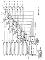
- a bubble memory device is designated by the reference numberal 10 is word organised and fault tolerant.
- a plurality of bubble memory chips 12, 14, 16, 18, 20, 22, 24, 26 provide individual bit outputs of a byte or word organised memory.
- Figure 1 shows an 8-bit device in which 8 bubble memory chips are provided with an additional ninth bubble memory chip 28 for the purpose of containing correction bits to be read into and read out of the bubble memory device in place of bits on the bubble memory chips 12 to 26. Any of the nine bubble memory chips may contain defective bits.
- the output of each of the bubble memory chips 12 to 26 is connected to a bit location in an output register. Bit locations 30, 32, 34, 36, 38, 40, 42, 44 are provided to be associated with bubble memory chips 12 to 26, respectively.
- the bubble memory chip 28 containing correction bits is connected with a correction bit line 46.
- the correction bit line 46 provides an input to each of a plurality of AND gates 48, 50, 52, 54, 56, 58, 60, 62.
- Each of the AND gates 48 to 62 has a data output connected to one of the bit locations 30 to 44, respectively, of the output register.
- Another path to the output register exists through AND gates 80 to 87 which is the normal path from the bubble memory chips 12 to 26 in the absence of errors.
- the bubble memory device 10 receives an input address from an address register 70.
- the address register 70 provides addresses on an address bus 72 which is connected with each of the bubble memory chips 12 to 28.
- the address bus 72 also provides an input to a Programmable Read Only Memory (PROM) 74.
- PROM Programmable Read Only Memory
- the PROM 74 has a 4-bit output and it may have an address range of 256 addresses.
- One of the outputs of the PROM 74 is provided on an enable decode line 76 which is connected with a decoder 78.
- the enable decode line 76 enables the decoder 78, which decodes input bits O-2 into an enable signal on only one of the eight output lines. The seven remaining decoder output lines are disabled.
- the particular enabled AND gate of the AND gates 48 to 62 channels the correction bit to the appropriate bit of the output register.
- the seven bits which are disabled cause their respective AND gates 80 to 87 to be enabled because of the logical inversion performed by inverters 90 to 97 on the signal from the decoder 78.
- FIG. 2 an example of the operation and required contents of the PROM 74 is shown with reference to the bubble memory device 10 in order to effect the correction process. Bits corresponding to faulty or bad minor loops are indicated by a square symbol as shown while an X indicates a logical "don't care" condition indicating that the result will be changed regardless of the PROM outputs going to the decoder.
- bit 3 of the PROM 74 contains binary 1's only for these addresses and O's for all others.
- the bits in error are (in right-to-left order): 3, 5, 5, 7. This corresponds to bit locations 36, 40, 40, and 44.
- the first three bits of the PROM 74, namely bits 0-2, contain these faulty bit locations at the respective bad major loop address locations. No modification of the data byte is required for bytes at major loop addresses where faulty bits are not present and thus a large number of "don't care" bits may exist in the correction bit bubble chip 28.
- Bit 3 at major loop address 1 shows a binary 1 and the correction bit is also a binary 1.
- Bit 5 at address 2 shows a binary 0 which is corrected to be a binary 1 using a correction bit from the correction bit chip 28.
- Bit 5 at address 252 shows a binary 1 which is corrected to be a binary 0 using a correction bit from chip 28.
- Bit 7 at address 254 shows a binary 0 corrected, coincidentally, to be a binary O.
- the correction bit may or may not be the same as the faulty bit from the particular bubble memory chip 12 to 26. Thus whilst the veracity of the error bit cannot be trusted the correction bit is known to be correct.
- the sequence of operations as shown in Figure 1 is merely reversed.
- the same PROM 74 is used to designate which bits need to be written into the correction bit chip 28 instead of, or alternatively in addition to, the normal bubble loop chip.
- the bubble memory device 10 has the very distinct advantage that no extra minor loops are required in the bubble memory chips to provide redundancy such as used in the prior art. When extra minor loops are required in addition to normal memory size, comparatively complex methods and hardware are needed to ensure synchronisation of the output of a word or byte organised memory and such systems require data deskewing or buffering techniques in order to provide for proper data flow.
- the present invention automatically provides for bit synchronisation and comparatively little additional hardware is required to implement the operation of the correction bit bubble memory chip 28.
- the bubble memory device described above is such that a testing process for the bubble memory chips will produce a map or list of the defective major loop address locations for each chip and the bubble memory chips can be sorted so that the bubble memory chips comprising a byte or word of a memory may be selected so that no two or more bubble memory chips have defective bits in the same major loop address positions.
- Each bubble memory chip need only have the number of major loop bit locations as required to maintain the nominal memory size.
- the above described bubble memory device has many advantages over the type of fault tolerant bubble memory device as shown in U.S. Patent Specification No. 3 909 810 in that the bubble memory device is not required to serve as a flag chip containing only information about defective byte locations.
- the above described bubble memory device uses only bubble memory chips for storage of data.
- the defective map memory device or flaw table, as it is sometimes called, of the present bubble memory chip is contained in the PROM 74.
- the above described bubble memory device has advantages over systems involving extra or redundant minor loops in bubble memory devices because such systems require some type of mechanism for compacting data or buffering data in order to compensate for interruptions in the regular flow of data from a bubble memory when a bit location is skipped as the device is read in a serial fashion.
Abstract
A bubble memory device of the word organised, fault tolerant type comprises a number of bubble memory chips (12-26) equivalent in number to a given word size, a correction bit bubble memory chip (28), a Programmable Read Only Memory (74) responsive to input addresses for identifying defective bit locations in the bubble memory chips, an address register (70) providing addresses to the PROM (74) and a decoder (78) substituting, in reading and writing operations, correction bits from the correction bit bubble memory chip (28) for bits in any one of the bubble memory chips in response to output signals from the PROM (74) identifying a defective bit location.
Description
- This invention relates to bubble memory devices and in particular to fault tolerance bubble memory devices.
- Herein a "byte" is defined as eight bits. A "word" can be any arbitrary number of bits.
- In conventional manufacturing processes for bubble memory chips, a certain number of bubble memory chips will be defective. Normal manufacturing control requires a trade-off between manufacturing 100% perfect bubble memory chips and testing after the manufacture to find defective but usable bubble memory chips. Various suggestions have been made to increase the yield of usable bubble memory chips by designing the bubble memory chip in such a way that a number of faults or defects may exist and yet the bubble memory chip is usable in the particular bubble memory device. Many fault tolerant bubble memory devices exist employing both external logic and memory as well as various modifications of the design of a standard bubble memory chip, or combinations of both.
- In U.S. Patent Specification No. 3 909 810 extra minor loops are included in each bubble memory chip in a bubble memory device and an external memory source is used together with logic devices to identify faulty minor loops which are to be ignored in favour of usable minor loops. Thus, all of the fault tolerant ability is based on external logic devices combined with the necessity of having bubble memory chips containing an excess number of minor loops.
- U.S. Patent Specification No. 3 792 450 discloses a major loop, minor loop bubble memory device having additional minor loops which are used for the purpose of containing a flaw table to identify the minor loop locations which are defective. The device provides for additional complexity to the individual bubble memory chips in that additional connections and read gates are required on the bubble memory chips to allow for independent reading of the minor loop flaw table. Thus, further care in design and construction of the individual bubble memory chips is required to ensure that proper synchronization is maintained between the redundant loops and the remainder of the bubble memory device so that the correct correspondence is maintained and identity between indications of faulty loops and the actual loops which are defective.
- According to the present invention there is provided a bubble memory device characterised by comprising: a plurality of bubble memory chips equivalent in number to a given word size; a correction bit bubble memory chip; memory means responsive to input addresses for identifying defective bit locations in said plurality of bubble memory chips; means for providing addresses to said memory means; and substituting means for substituting in reading and writing operations, correction bits from said correction bit bubble memory chip for bits in any one of said plurality of bubble memory chips in response to output signals from said memory means identifying a defective bit location.
- Said substituting means may comprise a decoder associated with an output-address from the said memory means for identifying a particular one of said plurality of bubble memory chips having a defective location and logic gate means which in response to a signal from said decoder connects said correction bit chip with the appropriate input or output of said memory device in reading and writing operations.
- Said logic gate means may be composed of AND gates.
- Preferably each said AND gate is connected to receive a common data bit input from said correction bit bubble memory chip and a unique input from said decoder for gating said input in response to an enable signal from said decoder further AND gate means being provided for disabling the output from any one of said bubble memory chips in response to an inverted enable signal from said decoder when a bit from said correction bit chip is to be gated. The bubble memory device may include means for disabling said decoder when no correction bit is to be gated.
- The invention is illustrated, merely by way of example, in the accompanying drawings, in which:-
- Figure 1 is a block schematic diagram of an embodiment of a bubble memory device according to the present invention; and
- Figure 2 is a logic chart illustrating the operating of the bubble memory device of Figure 1.
- Referring to Figure 1 a bubble memory device according to the present invention is designated by the reference numberal 10 is word organised and fault tolerant. A plurality of
bubble memory chips bubble memory chip 28 for the purpose of containing correction bits to be read into and read out of the bubble memory device in place of bits on thebubble memory chips 12 to 26. Any of the nine bubble memory chips may contain defective bits. The output of each of thebubble memory chips 12 to 26 is connected to a bit location in an output register.Bit locations bubble memory chips 12 to 26, respectively. Thebubble memory chip 28 containing correction bits is connected with acorrection bit line 46. Thecorrection bit line 46 provides an input to each of a plurality ofAND gates AND gates 48 to 62 has a data output connected to one of thebit locations 30 to 44, respectively, of the output register. In addition, another path to the output register exists through ANDgates 80 to 87 which is the normal path from thebubble memory chips 12 to 26 in the absence of errors. - The bubble memory device 10 receives an input address from an
address register 70. Theaddress register 70 provides addresses on anaddress bus 72 which is connected with each of thebubble memory chips 12 to 28. Theaddress bus 72 also provides an input to a Programmable Read Only Memory (PROM) 74. By way of example in the present embodiment the PROM 74 has a 4-bit output and it may have an address range of 256 addresses. One of the outputs of thePROM 74 is provided on an enabledecode line 76 which is connected with adecoder 78. The enabledecode line 76 enables thedecoder 78, which decodes input bits O-2 into an enable signal on only one of the eight output lines. The seven remaining decoder output lines are disabled. Hence, the particular enabled AND gate of theAND gates 48 to 62 channels the correction bit to the appropriate bit of the output register. The seven bits which are disabled cause their respective ANDgates 80 to 87 to be enabled because of the logical inversion performed by inverters 90 to 97 on the signal from thedecoder 78. - When the enable
decode line 76 is disabled, all decoder lines are disabled and consequently allAND gates 80 to 87 are enabled causing normal data flow from thebubble memory chips 12 to 26 to thebit locations 30 to 44. - Referring now to Figure 2, an example of the operation and required contents of the
PROM 74 is shown with reference to the bubble memory device 10 in order to effect the correction process. Bits corresponding to faulty or bad minor loops are indicated by a square symbol as shown while an X indicates a logical "don't care" condition indicating that the result will be changed regardless of the PROM outputs going to the decoder. - For the purposes of illustration in Figure 2, the major loop addresses in the bubble memory chips assumed to be faulty are 1, 2, 252 and 254.
Bit 3 of thePROM 74 contains binary 1's only for these addresses and O's for all others. The bits in error are (in right-to-left order): 3, 5, 5, 7. This corresponds tobit locations PROM 74, namely bits 0-2, contain these faulty bit locations at the respective bad major loop address locations. No modification of the data byte is required for bytes at major loop addresses where faulty bits are not present and thus a large number of "don't care" bits may exist in the correctionbit bubble chip 28. -
Bit 3 atmajor loop address 1 shows a binary 1 and the correction bit is also abinary 1.Bit 5 ataddress 2 shows a binary 0 which is corrected to be abinary 1 using a correction bit from thecorrection bit chip 28.Bit 5 ataddress 252 shows abinary 1 which is corrected to be a binary 0 using a correction bit fromchip 28. Bit 7 at address 254 shows a binary 0 corrected, coincidentally, to be a binary O. Note that the correction bit may or may not be the same as the faulty bit from the particularbubble memory chip 12 to 26. Thus whilst the veracity of the error bit cannot be trusted the correction bit is known to be correct. - For writing into the bubble memory device, the sequence of operations as shown in Figure 1 is merely reversed. The
same PROM 74 is used to designate which bits need to be written into thecorrection bit chip 28 instead of, or alternatively in addition to, the normal bubble loop chip. The bubble memory device 10 has the very distinct advantage that no extra minor loops are required in the bubble memory chips to provide redundancy such as used in the prior art. When extra minor loops are required in addition to normal memory size, comparatively complex methods and hardware are needed to ensure synchronisation of the output of a word or byte organised memory and such systems require data deskewing or buffering techniques in order to provide for proper data flow. The present invention automatically provides for bit synchronisation and comparatively little additional hardware is required to implement the operation of the correction bitbubble memory chip 28. - The bubble memory device described above is such that a testing process for the bubble memory chips will produce a map or list of the defective major loop address locations for each chip and the bubble memory chips can be sorted so that the bubble memory chips comprising a byte or word of a memory may be selected so that no two or more bubble memory chips have defective bits in the same major loop address positions. Each bubble memory chip need only have the number of major loop bit locations as required to maintain the nominal memory size.
- The above described bubble memory device has many advantages over the type of fault tolerant bubble memory device as shown in U.S. Patent Specification No. 3 909 810 in that the bubble memory device is not required to serve as a flag chip containing only information about defective byte locations. The above described bubble memory device uses only bubble memory chips for storage of data. The defective map memory device or flaw table, as it is sometimes called, of the present bubble memory chip is contained in the
PROM 74. Similarly, the above described bubble memory device has advantages over systems involving extra or redundant minor loops in bubble memory devices because such systems require some type of mechanism for compacting data or buffering data in order to compensate for interruptions in the regular flow of data from a bubble memory when a bit location is skipped as the device is read in a serial fashion.
Claims (5)
1. A bubble memory device characterised by comprising:
a plurality of bubble memory chips (12-26) equivalent in number to a given word size; a correction bit bubble memory chip (28), memory means (74) responsive to input addresses for identifying defective bit locations in said plurality of bubble memory chips; means (70) for providing addresses to said memory means; and substituting means (78) for substituting in reading and writing operations, correction bits from said correction bit bubble memory chip for bits in any one of said plurality of bubble memory chips in response to output signals from said memory means identifying a defective bit location.
2. A bubble memory device as claimed in claim 1 characterised in that said substituting means comprises a decoder (78) associated with an output address from said memory means (74) for identifying a particular one of said plurality of bubble memory chips having a defective location and logic gate means (48-62) which in response to a signal from said decoder connects said correction bit chip with the appropriate input or output of said memory device in reading and writing operations.
3. A bubble memory device as claimed in claim 2 characterised in that said logic gate means is composed of AND gates.
4. A bubble memory device as claimed in claim 3 characterised in that each of said AND gates is connected to receive a common data bit input from said correction bit bubble memory chip (28) and a unique input from said decoder (78) for gating said input in response to an enable signal from said decoder, further AND gate means (80-86) being provided for disabling the output from any one of said .bubble memory chips in response to an inverted enable signal from said decoder when a bit from said correction bit chip is to be gated.
5. A bubble memory device as claimed in claim 4 characterised by including means (76) for disabling said decoder when no correction bit is to be gated.
Applications Claiming Priority (2)
| Application Number | Priority Date | Filing Date | Title |
|---|---|---|---|
| US06/096,099 US4291389A (en) | 1979-11-20 | 1979-11-20 | Memory system using faulty bubble memory devices |
| US96099 | 1979-11-20 |
Publications (2)
| Publication Number | Publication Date |
|---|---|
| EP0029304A2 true EP0029304A2 (en) | 1981-05-27 |
| EP0029304A3 EP0029304A3 (en) | 1981-10-07 |
Family
ID=22255305
Family Applications (1)
| Application Number | Title | Priority Date | Filing Date |
|---|---|---|---|
| EP80303733A Withdrawn EP0029304A3 (en) | 1979-11-20 | 1980-10-22 | Bubble memory device |
Country Status (3)
| Country | Link |
|---|---|
| US (1) | US4291389A (en) |
| EP (1) | EP0029304A3 (en) |
| JP (1) | JPS599113B2 (en) |
Cited By (1)
| Publication number | Priority date | Publication date | Assignee | Title |
|---|---|---|---|---|
| GB2136992A (en) * | 1983-03-18 | 1984-09-26 | Georg V Coza | Method and System of Ensuring Integrity of Data in an Electronic Memory |
Families Citing this family (3)
| Publication number | Priority date | Publication date | Assignee | Title |
|---|---|---|---|---|
| US4453248A (en) * | 1982-06-16 | 1984-06-05 | International Business Machines Corporation | Fault alignment exclusion method to prevent realignment of previously paired memory defects |
| US4479214A (en) * | 1982-06-16 | 1984-10-23 | International Business Machines Corporation | System for updating error map of fault tolerant memory |
| US4759020A (en) * | 1985-09-25 | 1988-07-19 | Unisys Corporation | Self-healing bubble memories |
Citations (2)
| Publication number | Priority date | Publication date | Assignee | Title |
|---|---|---|---|---|
| US3868646A (en) * | 1972-06-09 | 1975-02-25 | Ericsson Telefon Ab L M | Memory device with standby memory elements |
| DE2817134A1 (en) * | 1977-04-20 | 1978-11-02 | Hitachi Ltd | MEMORY CONTROL SYSTEM |
Family Cites Families (1)
| Publication number | Priority date | Publication date | Assignee | Title |
|---|---|---|---|---|
| FR2307332A1 (en) * | 1975-04-07 | 1976-11-05 | Sperry Rand Corp | PROCESS FOR STORING INFORMATION IN A MEMORY INCLUDING AT LEAST ONE DEFECTIVE STORAGE ZONE AND DEVICE FOR EXECUTION OF THIS PROCESS |
-
1979
- 1979-11-20 US US06/096,099 patent/US4291389A/en not_active Expired - Lifetime
-
1980
- 1980-10-20 JP JP55146767A patent/JPS599113B2/en not_active Expired
- 1980-10-22 EP EP80303733A patent/EP0029304A3/en not_active Withdrawn
Patent Citations (2)
| Publication number | Priority date | Publication date | Assignee | Title |
|---|---|---|---|---|
| US3868646A (en) * | 1972-06-09 | 1975-02-25 | Ericsson Telefon Ab L M | Memory device with standby memory elements |
| DE2817134A1 (en) * | 1977-04-20 | 1978-11-02 | Hitachi Ltd | MEMORY CONTROL SYSTEM |
Non-Patent Citations (1)
| Title |
|---|
| IBM TECHNICAL DISCLOSURE BULLETIN, vol. 10, no. 10, March 1968, pages 1553-1554, New York, U.S.A., J.B. GILLETT: "System for bypassing defective memory elements" * |
Cited By (1)
| Publication number | Priority date | Publication date | Assignee | Title |
|---|---|---|---|---|
| GB2136992A (en) * | 1983-03-18 | 1984-09-26 | Georg V Coza | Method and System of Ensuring Integrity of Data in an Electronic Memory |
Also Published As
| Publication number | Publication date |
|---|---|
| US4291389A (en) | 1981-09-22 |
| JPS5674886A (en) | 1981-06-20 |
| JPS599113B2 (en) | 1984-02-29 |
| EP0029304A3 (en) | 1981-10-07 |
Similar Documents
| Publication | Publication Date | Title |
|---|---|---|
| US6484271B1 (en) | Memory redundancy techniques | |
| CA1056952A (en) | Error detection and correction in data processing systems | |
| US3659275A (en) | Memory correction redundancy system | |
| US3681757A (en) | System for utilizing data storage chips which contain operating and non-operating storage cells | |
| US4982360A (en) | Memory subsystem | |
| US3588830A (en) | System for using a memory having irremediable bad bits | |
| US5925138A (en) | Method for allowing data transfers with a memory having defective storage locations | |
| JPH0668700A (en) | Semiconductor memory device | |
| JPS6112292B2 (en) | ||
| EP0363031B1 (en) | Serial input/output semiconductor memory | |
| US4689792A (en) | Self test semiconductor memory with error correction capability | |
| EP0096780B1 (en) | A fault alignment exclusion method to prevent realignment of previously paired memory defects | |
| JP2539343B2 (en) | Error correction circuit with simplified syndrome word and correction method | |
| EP0029304A2 (en) | Bubble memory device | |
| US4884194A (en) | Multiprocessor computer system which includes N parallel-operating modules and an external apparatus, and computer module for use in such a system | |
| US5337317A (en) | Minimizing the programming time in a semiconductor integrated memory circuit having an error correction function | |
| JPH0544760B2 (en) | ||
| JPS61222097A (en) | Bit line mutual array type rom | |
| US4145757A (en) | Fault tolerant bubble memory with redundancy using a stationary register on a single chip | |
| CA1182917A (en) | Memory system using faulty bubble memory devices | |
| US5255217A (en) | Integrated circuit memory device with a redundant memory block | |
| US4187554A (en) | Fault tolerant bubble memory with redundancy using a stationary register on a single chip | |
| JPS6357819B2 (en) | ||
| JPH10143445A (en) | Satellite line connector | |
| JPS58200351A (en) | Error correcting circuit |
Legal Events
| Date | Code | Title | Description |
|---|---|---|---|
| PUAI | Public reference made under article 153(3) epc to a published international application that has entered the european phase |
Free format text: ORIGINAL CODE: 0009012 |
|
| AK | Designated contracting states |
Designated state(s): DE FR GB |
|
| PUAL | Search report despatched |
Free format text: ORIGINAL CODE: 0009013 |
|
| AK | Designated contracting states |
Designated state(s): DE FR GB |
|
| 17P | Request for examination filed |
Effective date: 19811015 |
|
| STAA | Information on the status of an ep patent application or granted ep patent |
Free format text: STATUS: THE APPLICATION IS DEEMED TO BE WITHDRAWN |
|
| 18D | Application deemed to be withdrawn |
Effective date: 19850426 |
|
| RIN1 | Information on inventor provided before grant (corrected) |
Inventor name: TOTH, DOLAN HAROLD |