EP0021289B1 - Constant current circuit - Google Patents
Constant current circuit Download PDFInfo
- Publication number
- EP0021289B1 EP0021289B1 EP80103322A EP80103322A EP0021289B1 EP 0021289 B1 EP0021289 B1 EP 0021289B1 EP 80103322 A EP80103322 A EP 80103322A EP 80103322 A EP80103322 A EP 80103322A EP 0021289 B1 EP0021289 B1 EP 0021289B1
- Authority
- EP
- European Patent Office
- Prior art keywords
- constant current
- mos transistor
- power source
- drain
- current circuit
- Prior art date
- Legal status (The legal status is an assumption and is not a legal conclusion. Google has not performed a legal analysis and makes no representation as to the accuracy of the status listed.)
- Expired
Links
- 238000010586 diagram Methods 0.000 description 11
- 230000004048 modification Effects 0.000 description 8
- 238000012986 modification Methods 0.000 description 8
- 239000013078 crystal Substances 0.000 description 4
- 239000000758 substrate Substances 0.000 description 4
- 230000000694 effects Effects 0.000 description 3
- 238000004519 manufacturing process Methods 0.000 description 3
- 239000004065 semiconductor Substances 0.000 description 3
- 239000003990 capacitor Substances 0.000 description 2
- 230000002238 attenuated effect Effects 0.000 description 1
- 238000010276 construction Methods 0.000 description 1
- 102220051100 rs199575734 Human genes 0.000 description 1
Images


Classifications
-
- G—PHYSICS
- G05—CONTROLLING; REGULATING
- G05F—SYSTEMS FOR REGULATING ELECTRIC OR MAGNETIC VARIABLES
- G05F3/00—Non-retroactive systems for regulating electric variables by using an uncontrolled element, or an uncontrolled combination of elements, such element or such combination having self-regulating properties
- G05F3/02—Regulating voltage or current
- G05F3/08—Regulating voltage or current wherein the variable is DC
- G05F3/10—Regulating voltage or current wherein the variable is DC using uncontrolled devices with non-linear characteristics
- G05F3/16—Regulating voltage or current wherein the variable is DC using uncontrolled devices with non-linear characteristics being semiconductor devices
- G05F3/20—Regulating voltage or current wherein the variable is DC using uncontrolled devices with non-linear characteristics being semiconductor devices using diode- transistor combinations
- G05F3/26—Current mirrors
- G05F3/262—Current mirrors using field-effect transistors only
Definitions
- the present invention relates to a constant current circuit.
- the constant current circuit has a function to provide a constant current. Also in case where there is a variation in the threshold voltages of MOS FETs constituting the constant current circuit, it is required to keep constant the current fed by the constant current circuit.
- the constant current circuit in Fig. 1 has a P channel MOS FET 10 which is connected at the source and substrate to the first power source terminal 2, and at the gate to the second power source terminal 4 and an N channel MOS FET 12 which is connected at the gate and drain commonly to the drain of the FET 10, and at the source to a second power source terminal.
- the drain of the N channel MOS FET 12 is coupled with the gate of an N channel MOS FET 14 which is connected at the drain to the first power source terminal 2 by way of a load 16, and at the substrate and the source to the second power source terminal 4.
- the variation of the threshold voltages of the FETs is unavoidable in the manufacturing process of the semiconductor components. Because of the presence of the unavoidable variation of threshold voltages, when a number of FETs are integrated on a single semiconductor substrate, a constant current obtained in each constant current circuit will have a different value in accordance with the variation of the threshold voltages of the FETs.
- a constant current circuit shown in Fig. 2 is so designed as to remedy the disadvantage of the constant current circuit of Fig. 1 that the drain current of the FET 10 varies with the variation of the power source voltage.
- the enhancement type MOS FET 10 used in the circuit of Fig. 1 is replaced by a depletion type MOS FET 18.
- the voltage between the source and gate of the FET 18 in the constant current circuit of Fig. 2 is kept at OV, so that the drain current of the FET 18 does not change and consequently the drain current of the FET 14 little changes.
- a variation of the threshold voltages occurring in the manufacturing process causes the desired constant current to change.
- the ordinary CMOS integrated circuit uses enhancement type MOS FETs. In constructing such CMOS integrated circuit, if a depletion type MOS FET is used for one of the FETs, the steps of the manufacturing process of the circuit must be increased correspondingly.
- FIG. 3 An example shown in Fig. 3 uses a resistor 20 in place of the FET 10 used in the constant current circuit shown in Fig. 1.
- the preset current values do not vary even if the threshold voltages of the FETs vary.
- the magnitude of the current flowing into the resistor 20 linearly changes, so that the current flowing into the load 16 also changes.
- the constant current circuit of Fig. 4 is comprised of a P channel MOS FET 22 and an N channel MOS FET 24, which are in series between the power source terminals 2 and 4, and a P channel MOS FET 26, an N channel MOS FET 28 and a resistor 30, which are connected in series between the power source terminals 2 and 4.
- the gate of the FET 22 is connected to the gate and the drain of the FET 26.
- the gate of the FET 28 is connected to the gate of an N channel MOS FET 14, and the gate and the drain of the FET 24.
- the FET 14 in cooperation with the FETs 24 and 28, constitutes a current mirror circuit which feeds a constant current to the load 16.
- the channel constants of the FETs 22, 24, 26,28 and 14 which are defined by the channel width/channel length of each of those FETs, are S22, S24, S26, S28 and S14, respectively.
- the drain currents 11 and 12 of the FETs 22 and 26 are given by the following equations: where I C1 is a constant, e is the base of a Napierian logarithm, K is a constant, V1 is a drain voltage of the FET 24, and R30 is a resistance of the resistor 30.
- an object of the present invention is to provide a constant current circuit which is capable of feeding a constant current without being influenced by a variation of the power source voltage.
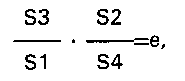
- a constant current circuit comprising first and second MOS trans- sistors of different channel types of which the current paths are connected in series between first and second power source terminals; a third MOS transistor of the same channel type as that of said first MOS transistor which is connected to said first power source terminal and said first MOS transistor to form a constant current means in cooperation with said first MOS transistor; a fourth MOS transistor of the same channel type as that of said second MOS transistor, which has a drain connected to the gate of said second MOS transistor and a current path connected in series with the current path of said third MOS transistor between said first and second power source terminals, and a fifth MOS transistor whose gate voltage is controlled in accordance with the current fed from said constant current means to feed a constant current to a load, further comprising resistive means which is connected at one end to the drain of said fourth MOS transistor and at the other end to the gate of said fourth MOS transistor and the drain of said third MOS transistor, and the gate of said fifth MOS transistor is
- FR-A-2 301 861 discloses a constant current circuit wherein first and second transistors of different types (PNP and NPN) are connected in series between first and second power source terminals.
- a third transistor of the same type as that of the first transistor forms in cooperation with the latter a constant current means (current mirror circuit).
- a fourth transistor of the same type as that of the second transistor has its collector connected to the base of the second transistor.
- Third and fourth transistors form a current path across resistive means which is connected at one end to the collector of the fourth transistor and at the other end to the base of the fourth transistor and the collector of the third transistor.
- further transistors comprising a fifth transistor whose base is coupled to the collector of the fourth transistor.
- Fig. 5 illustrating a constant current circuit according to an embodiment of the present invention.
- the constant current circuit shown in Fig. 5 has a series circuit including a P channel MOS FET 56, a resistor 58 and an N channel MOS FET 60, which is connected between positive and negative power source terminals 52 and 54.
- the resistor 58 is connected between FETs 56 and 60 of which the sources are respectively connected to the power source terminals 52 and 54.
- the gate of the FET 60 is coupled with the drain of the FET 56.
- Further connected between the power source terminals 52 and 54 is a series circuit of a P channel MOS FET 62 and an N channel MOS FET 64.
- the gate and drain of the FET 62 are coupled with the gate of the FET 56.
- the gate and drain of the FET 64 are coupled with the drain of the FET 60 and the drain of the FET 62 respectively.
- the drain of the FET 60 is coupled with the gate of an N channel MOS FET 66 which is connected at the drain to the power source terminal 52 through a load 68 and at the source to the power source terminal 54.
- the FETs 56 and 62 cooperate to form a current mirror circuit and the FETs 64 and 66 cooperate to form a current mirror circuit.
- the drain currents flowing through FETs 56, 62 and 66 are I D1' I D2 and I D3' and the channel constants of the FETs 56, 60, 62, 64 and 66 are S56, S60, S62, S64 and S66.
- R58 is a resistance of the resistor 58.
- each enhancement type MOS FET therein is set so as to operate in the tailing operation region of a drain current-gate voltage characteristic, in principle.
- a drain current-gate voltage characteristic in principle.
- the drain current I D of the MOS FET operating in the tailing region is generally expressed by where I c and K are each constant, S is the ratio of channel width/channel length, e is the base of a Napierian logarithm, V is the gate voltage, and V TH is a threshold voltage.
- the drain current in the constant current circuit is independent of the threshold voltage of each MOS FET and the power source voltage as well, but depends on the ratio of the channel constants of respective FETs, the resistor 58 and the characteristic constant K (corresponding to an inclination of the characteristic curve in the tailing operation region) of each FET.
- the drain voltage V56 of the FET 56 under a balanced condition by AV56.
- the amounts of change of the drainucucrents of the FETs 60 and 56 denoted as ⁇ I D11 and ⁇ I D12
- the amounts of change of the drain currents of the FETs 60 and 56 denoted as I D2
- Olp z is zero and the noise in the drain of the FET 56 has no influence on the drain current I D2 of the FET 62. Therefore, the current flowing through the load 68 is also invariable. Thus, the stability of the operation against the noise is effectively improved.
- Fig. 6 there is shown another embodiment of the constant current circuit according to the invention, in which the load current setting range may be set more widely than the constant current circuit shown in Fig. 5.
- the constant current circuit shown in Fig. 6 is the same as that of Fig. 5, except that a resistor 70 is connected between the source of the MOS FET 64 and the power source terminal 54.
- the constant current circuit shown in Fig. 6 may obtain a constant current which may be set in a wider range than the circuit shown in Fig. 5. Also, in this case, the constant current is little influenced by a variation of the threshold voltage of each MOS FET used in the constant current circuit and a variation of the power source voltage.
- a constant current circuit shown in Fig. 7 uses a crystal oscillator circuit as the load 68 in the constant current circuit shown in Fig. 6.
- the load 68 is comprised of MOS FETs 72 and 74 of P and N channel types having current paths connected in series between the power source terminal 52 and an MOS FET 66, a capacitor 76 connected between the gates of the MOS FETs 72 and 74 and a power source terminal Vs, a capacitor 78 connected between the power source terminal Vs and an output terminal Vo connected to the drains of the MOS FETs 72 and 74, an N channel MOS FET 80 connected at the gate to the power source terminal Vp and a P channel MOS FET 82 connected at the gate to the power source terminal Vs, which are connected in parallel between the output terminal Vo and the gates of the MOS FETs 72 and 74, and a crystal resonator 84 connected between the output terminal Vo and the gates of the FETs 72 and 74.
- the dissipation current rapidly increases with increase of the power source voltage. Thus, it is very difficult to restrict the dissipation current to a small value.
- the increase of the dissipation current is merely about 20%. In this case, the value of the dissipation current may also be restricted to a small value. The result is that the power consumption is small.
- Fig. 8 shows a modification of the constant current circuit shown in Fig. 5.
- a P channel MOS FET 86 in place of the N channel MOS FET 66, is coupled with the load 68.
- the gate of the P channel MOS FET 86 is coupled with the drain of a P channel MOS FET 62.
- the embodiment shown in Fig. 8 may also attain the effects similar to that by the constant current circuit shown in Fig. 5.
- a resistor 88 may be coupled between the power source terminal 52 and the sources of the MOS FETs 56 and 62 as shown in Fig. 9 in order to obtain a similar function to that of the resistor 70 of Fig. 6.
- Fig. 10 shows a modification of the constant current circuit shown in Fig. 9, in which the resistor 88 used in the constant current circuit shown in Fig. 9 is removed and a resistor 90 is coupled between the source of an MOS transistor 64 of an N channel and the power source terminal 54.
- the constant current circuit shown in Fig. 10 operates in principle like the circuit shown in Fig. 9, thus having a similar effect to that of the same.
- Fig. 11 shows a modification of the constant current circuit shown in Fig. 6.
- the resistor 70 used in the constant current circuit shown in Fig. 6 is removed and a resistor 92 is coupled between the source of the N channel MOS transistor 64 and the power source terminal 54.
- the constant current circuit shown in Fig. 11 also operates in principle like the circuit shown in Fig. 6, and thus has a similar effect.
Landscapes
- Engineering & Computer Science (AREA)
- Microelectronics & Electronic Packaging (AREA)
- Physics & Mathematics (AREA)
- Nonlinear Science (AREA)
- Electromagnetism (AREA)
- General Physics & Mathematics (AREA)
- Radar, Positioning & Navigation (AREA)
- Automation & Control Theory (AREA)
- Control Of Electrical Variables (AREA)
Description
- The present invention relates to a constant current circuit.
- It has been well known that a plurality of circuit components are formed on a single semiconductor substrate in the form of an integrated circuit, and the integrated circuit, after being incorporated into an electronic clock circuit or a desk-top type calculator, is driven by a battery or the like. In this case, in order to elongate the life time of the drive battery as long as possible, it is desirable to restrict the power consumption in the integrated circuit as small as possible. In the integrated circuit containing the constant current circuit, for example, it is required to minimize the power consumption in the constant current circuit so long as a proper circuit operation related is ensured. When a dry cell is used for the drive power source, the output voltage of the dry cell greatly varies with the lapse of time. In this respect, also when the power source voltage varies, it is desirable that the constant current circuit has a function to provide a constant current. Also in case where there is a variation in the threshold voltages of MOS FETs constituting the constant current circuit, it is required to keep constant the current fed by the constant current circuit.
- To satisfy those requirements, there has been proposed a constant current circuit constructed as shown in Fig. 1, for example. The constant current circuit in Fig. 1 has a P
channel MOS FET 10 which is connected at the source and substrate to the firstpower source terminal 2, and at the gate to the secondpower source terminal 4 and an N channel MOS FET 12 which is connected at the gate and drain commonly to the drain of theFET 10, and at the source to a second power source terminal. The drain of the N channel MOS FET 12 is coupled with the gate of an Nchannel MOS FET 14 which is connected at the drain to the firstpower source terminal 2 by way of aload 16, and at the substrate and the source to the secondpower source terminal 4. - In the constant current circuit shown in Fig. 1, when the power source voltage applied between the
power source terminals FET 10. Since theFETs FET 10 is constant, a constant current flows into the drain of theFET 14, too. As a result, the current flowing through theload 16 is made constant. When the power source voltage varies, however, a voltage between the source and gate of theFET 10 varies thereby to vary the drain current of theFET 10. The variation of the drain current of theFET 10 causes the gate potential and the drain potential of theFET 12 to vary. As a result, a current proportional to a channel constant S defined by the channel width/channel length of each FET flows into theFETs load 16 also varies with the variation of the power source voltage. - The variation of the threshold voltages of the FETs is unavoidable in the manufacturing process of the semiconductor components. Because of the presence of the unavoidable variation of threshold voltages, when a number of FETs are integrated on a single semiconductor substrate, a constant current obtained in each constant current circuit will have a different value in accordance with the variation of the threshold voltages of the FETs.
- A constant current circuit shown in Fig. 2 is so designed as to remedy the disadvantage of the constant current circuit of Fig. 1 that the drain current of the
FET 10 varies with the variation of the power source voltage. In the constant current circuit shown in Fig. 2, the enhancement type MOS FET 10 used in the circuit of Fig. 1 is replaced by a depletion type MOS FET 18. When the power source voltage varies, the voltage between the source and gate of theFET 18 in the constant current circuit of Fig. 2 is kept at OV, so that the drain current of theFET 18 does not change and consequently the drain current of theFET 14 little changes. A variation of the threshold voltages occurring in the manufacturing process, however, causes the desired constant current to change. The ordinary CMOS integrated circuit uses enhancement type MOS FETs. In constructing such CMOS integrated circuit, if a depletion type MOS FET is used for one of the FETs, the steps of the manufacturing process of the circuit must be increased correspondingly. - An example shown in Fig. 3 uses a resistor 20 in place of the
FET 10 used in the constant current circuit shown in Fig. 1. In this circuit construction, the preset current values do not vary even if the threshold voltages of the FETs vary. However, when the power source voltage changes, the magnitude of the current flowing into the resistor 20 linearly changes, so that the current flowing into theload 16 also changes. - A constant current circuit designed to remedy the disadvantages of the constant current circuits of Figs. 1 to 3 is illustrated in Fig. 4. As shown, the constant current circuit of Fig. 4 is comprised of a P
channel MOS FET 22 and an N channel MOS FET 24, which are in series between thepower source terminals channel MOS FET 26, an Nchannel MOS FET 28 and a resistor 30, which are connected in series between thepower source terminals - In the constant current circuit, the FET 14, in cooperation with the FETs 24 and 28, constitutes a current mirror circuit which feeds a constant current to the
load 16. - Assume now that the channel constants of the
FETs drain currents 11 and 12 of theFETs 

FET 24, and R30 is a resistance of the resistor 30. - Since the
FETs currents 11 and 12 holds:
- 12=1/(K . R30) - loge{S28/S24 · S22/S26} (4)
- When the voltage at the junction between the
FETs FETs FETs value 12 obtained in the balanced state by an amount A12. In this case, the following equations hold:


- From the equations (5), (7) and (8), a gain of a loop including
MOS FETs 

S28/S24. S22/S26>1, ΔI11/ΔI12<1.
The noise is attenuated while it travels the loop; however, it is impossible to reduce it to zero, in principle. - Accordingly, an object of the present invention is to provide a constant current circuit which is capable of feeding a constant current without being influenced by a variation of the power source voltage.
- According to one aspect to the present invention, there is provided a constant current circuit comprising first and second MOS trans- sistors of different channel types of which the current paths are connected in series between first and second power source terminals; a third MOS transistor of the same channel type as that of said first MOS transistor which is connected to said first power source terminal and said first MOS transistor to form a constant current means in cooperation with said first MOS transistor; a fourth MOS transistor of the same channel type as that of said second MOS transistor, which has a drain connected to the gate of said second MOS transistor and a current path connected in series with the current path of said third MOS transistor between said first and second power source terminals, and a fifth MOS transistor whose gate voltage is controlled in accordance with the current fed from said constant current means to feed a constant current to a load, further comprising resistive means which is connected at one end to the drain of said fourth MOS transistor and at the other end to the gate of said fourth MOS transistor and the drain of said third MOS transistor, and the gate of said fifth MOS transistor is coupled to the drain of one of said first and fourth MOS transistors, said second, fourth and fifth MOS transistors each being set to operate in the tailing operation region of drain current-gate voltage characteristic, and the channel constant S1, S2, S3 and S4 each representing the ratio of channel width channel length of a corresponding one of said first to fourth MOS transistors (62, 64, 56, 60) being determined to have a relationship expressed as follows:
- FR-A-2 301 861 discloses a constant current circuit wherein first and second transistors of different types (PNP and NPN) are connected in series between first and second power source terminals. A third transistor of the same type as that of the first transistor forms in cooperation with the latter a constant current means (current mirror circuit). A fourth transistor of the same type as that of the second transistor has its collector connected to the base of the second transistor. Third and fourth transistors form a current path across resistive means which is connected at one end to the collector of the fourth transistor and at the other end to the base of the fourth transistor and the collector of the third transistor. In a similar circuit disclosed in FR-A-2 301 861, too, there are provided further transistors, comprising a fifth transistor whose base is coupled to the collector of the fourth transistor.
- The present invention will be better understood from the following description taken in connection with the accompanying drawings, in which:
- Fig. 1 is a circuit diagram of a conventional constant current circuit constructed by using enhancement type MOS FETs;
- Fig. 2 is a circuit diagram of another conventional constant current circuit in which one of the enhancement type MOS FETs used in the constant current circuit shown in Fig. 1 is replaced by a depletion type MOS FET;
- Fig. 3 is a circuit diagram of yet another conventional constant current circuit in which one of the MOS FETs used in the constant current circuit shown in Fig. 1 is replaced by a resistor;
- Fig. 4 is a circuit diagram of still another conventional constant current circuit designed to solve the problems involved in the operations of the constant current circuits of Figs. 1 to 3;
- Fig. 5 is a circuit diagram of a constant current circuit according to an embodiment of the present invention;
- Fig. 6 is a circuit diagram of a constant current circuit according to another embodiment of the present invention in which a variable range of the present constant current is widened;
- Fig. 7 is a circuit diagram of a constant current circuit which uses a crystal oscillating circuit as a load used in the constant current circuit shown in Fig. 6;
- Fig. 8 is a circuit diagram of a modification of the constant current circuit shown in Fig. 5;
- Fig. 9 is a circuit diagram of a modification of the constant current circuit shown in Fig. 8;
- Fig. 10 is a circuit diagram of a modification of the constant current circuit shown in Fig. 9; and
- Fig. 11 is a circuit diagram of a modification of the constant current circuit shown in Fig. 6.
- Reference is first made to Fig. 5 illustrating a constant current circuit according to an embodiment of the present invention. The constant current circuit shown in Fig. 5 has a series circuit including a P
channel MOS FET 56, aresistor 58 and an Nchannel MOS FET 60, which is connected between positive and negativepower source terminals resistor 58 is connected betweenFETs power source terminals FET 60 is coupled with the drain of theFET 56. Further connected between thepower source terminals channel MOS FET 62 and an Nchannel MOS FET 64. - The gate and drain of the
FET 62 are coupled with the gate of theFET 56. The gate and drain of theFET 64 are coupled with the drain of theFET 60 and the drain of theFET 62 respectively. The drain of theFET 60 is coupled with the gate of an Nchannel MOS FET 66 which is connected at the drain to thepower source terminal 52 through aload 68 and at the source to thepower source terminal 54. - The
FETs FETs - Assume that, in the constant current circuit shown in Fig. 5 under a balanced condition, the drain currents flowing through
FETs FETs 

FETs 
resistor 58. When a gate voltage equal to the gate voltage V60 is applied to the gate of theFET 66, the drain current ID4 flowing through theFET 64 is given by the following equation:
- Arranging the equation (13), ID2/ID4 is given

- Therefore, the voltage drop across the
resistor 58 causes the gate voltage of theFET 64 to drop below the gate voltage V60, so that a reduction rate of the drain current flowing through theFET 64 becomes equal to
S64/S60 . S56/S62
must be larger than 1. - In the constant current circuit shown in Fig. 5, each enhancement type MOS FET therein is set so as to operate in the tailing operation region of a drain current-gate voltage characteristic, in principle. Thus, by using such a characteristic region that the drain current exponentially changes with respect to the gate voltage, it is possible to obtain a stable constant current circuit. For this reason, the explanation to follow will proceed on the assumption that the enhancement type MOS FETs operate in the tailing region of the characteristic.
- The drain current ID of the MOS FET operating in the tailing region is generally expressed by

- If IO=IC · e-KVTH the equation (15) is rewritten as follows:

FETs 


- As seen from the equations (20), (21) and (22), the drain current in the constant current circuit is independent of the threshold voltage of each MOS FET and the power source voltage as well, but depends on the ratio of the channel constants of respective FETs, the
resistor 58 and the characteristic constant K (corresponding to an inclination of the characteristic curve in the tailing operation region) of each FET. - The explanation to follow is for a current changing rate when a noise, for example, is introduced into the constant current circuit.
- Assume that the noise introduced changes. the drain voltage V56 of the
FET 56 under a balanced condition by AV56. As described above relating to the constant current circuit shown in Fig. 4, the amounts of change of the drainucucrents of theFETs FETs 



FET 56 has no influence on the drain current ID2 of theFET 62. Therefore, the current flowing through theload 68 is also invariable. Thus, the stability of the operation against the noise is effectively improved. - In the constant current circuit shown in Fig. 5, all the MOS FETs are operated in the trailing region, so that the constant current value to be set is limited to an extremely small, so that an extremely small current flows into the
MOS FETs load 68 to some extent. Generally, the channel constant ratio S66/S64 is extremely large. Therefore, the range of a presettable constant current to be allowed to flow into theload 68 actually is restricted. - Turning now to Fig. 6, there is shown another embodiment of the constant current circuit according to the invention, in which the load current setting range may be set more widely than the constant current circuit shown in Fig. 5. The constant current circuit shown in Fig. 6 is the same as that of Fig. 5, except that a
resistor 70 is connected between the source of theMOS FET 64 and thepower source terminal 54. - In the constant current circuit shown in Fig. 6, the current Il flowing through the
load 68 is given by the following equation:

- As seen from the above equation, the constant current circuit shown in Fig. 6 may obtain a constant current which may be set in a wider range than the circuit shown in Fig. 5. Also, in this case, the constant current is little influenced by a variation of the threshold voltage of each MOS FET used in the constant current circuit and a variation of the power source voltage.
- A constant current circuit shown in Fig. 7 uses a crystal oscillator circuit as the
load 68 in the constant current circuit shown in Fig. 6. In the constant current circuit shown in Fig. 7, theload 68 is comprised ofMOS FETs power source terminal 52 and anMOS FET 66, acapacitor 76 connected between the gates of theMOS FETs MOS FETs channel MOS FET 80 connected at the gate to the power source terminal Vp and a Pchannel MOS FET 82 connected at the gate to the power source terminal Vs, which are connected in parallel between the output terminal Vo and the gates of theMOS FETs FETs - In an ordinary crystal oscillator circuit, the dissipation current rapidly increases with increase of the power source voltage. Thus, it is very difficult to restrict the dissipation current to a small value. On the other hand, in the circuit shown in Fig. 7, when the power source voltage is changed from 1.0V to 3.0V, the increase of the dissipation current is merely about 20%. In this case, the value of the dissipation current may also be restricted to a small value. The result is that the power consumption is small.
- Fig. 8 shows a modification of the constant current circuit shown in Fig. 5. In the constant current circuit, a P
channel MOS FET 86, in place of the Nchannel MOS FET 66, is coupled with theload 68. The gate of the Pchannel MOS FET 86 is coupled with the drain of a Pchannel MOS FET 62. The embodiment shown in Fig. 8 may also attain the effects similar to that by the constant current circuit shown in Fig. 5. - While having been described by using some specific embodiments, the invention may be modified variously within the scope of the spirit of the invention.
- For example, in the constant current circuit shown in Fig. 8, a
resistor 88 may be coupled between thepower source terminal 52 and the sources of theMOS FETs resistor 70 of Fig. 6. - Fig. 10 shows a modification of the constant current circuit shown in Fig. 9, in which the
resistor 88 used in the constant current circuit shown in Fig. 9 is removed and aresistor 90 is coupled between the source of anMOS transistor 64 of an N channel and thepower source terminal 54. The constant current circuit shown in Fig. 10 operates in principle like the circuit shown in Fig. 9, thus having a similar effect to that of the same. - Fig. 11 shows a modification of the constant current circuit shown in Fig. 6. In this modification, the
resistor 70 used in the constant current circuit shown in Fig. 6 is removed and aresistor 92 is coupled between the source of the Nchannel MOS transistor 64 and thepower source terminal 54. The constant current circuit shown in Fig. 11 also operates in principle like the circuit shown in Fig. 6, and thus has a similar effect.
Claims (11)

Applications Claiming Priority (2)
| Application Number | Priority Date | Filing Date | Title |
|---|---|---|---|
| JP7627879A JPS562017A (en) | 1979-06-19 | 1979-06-19 | Constant electric current circuit |
| JP76278/79 | 1979-06-19 |
Publications (2)
| Publication Number | Publication Date |
|---|---|
| EP0021289A1 EP0021289A1 (en) | 1981-01-07 |
| EP0021289B1 true EP0021289B1 (en) | 1984-12-12 |
Family
ID=13600798
Family Applications (1)
| Application Number | Title | Priority Date | Filing Date |
|---|---|---|---|
| EP80103322A Expired EP0021289B1 (en) | 1979-06-19 | 1980-06-13 | Constant current circuit |
Country Status (4)
| Country | Link |
|---|---|
| US (1) | US4327321A (en) |
| EP (1) | EP0021289B1 (en) |
| JP (1) | JPS562017A (en) |
| DE (1) | DE3069787D1 (en) |
Families Citing this family (52)
| Publication number | Priority date | Publication date | Assignee | Title |
|---|---|---|---|---|
| FR2494519A1 (en) * | 1980-11-14 | 1982-05-21 | Efcis | INTEGRATED CURRENT GENERATOR IN CMOS TECHNOLOGY |
| GB2090442B (en) * | 1980-12-10 | 1984-09-05 | Suwa Seikosha Kk | A low voltage regulation circuit |
| GB2093303B (en) * | 1981-01-20 | 1985-05-22 | Citizen Watch Co Ltd | Voltage sensing circuit |
| DE3360366D1 (en) * | 1982-02-26 | 1985-08-14 | Toshiba Kk | Mos switch circuit |
| JPS5992910U (en) * | 1982-12-09 | 1984-06-23 | 日産自動車株式会社 | constant current circuit |
| NL8302731A (en) * | 1983-08-02 | 1985-03-01 | Philips Nv | SEMICONDUCTOR DEVICE. |
| US4550284A (en) * | 1984-05-16 | 1985-10-29 | At&T Bell Laboratories | MOS Cascode current mirror |
| US4583037A (en) * | 1984-08-23 | 1986-04-15 | At&T Bell Laboratories | High swing CMOS cascode current mirror |
| JPH0810415B2 (en) * | 1984-12-04 | 1996-01-31 | 日本電気株式会社 | Reference voltage source |
| US4599554A (en) * | 1984-12-10 | 1986-07-08 | Texet Corportion | Vertical MOSFET with current monitor utilizing common drain current mirror |
| US4618815A (en) * | 1985-02-11 | 1986-10-21 | At&T Bell Laboratories | Mixed threshold current mirror |
| JPH0640290B2 (en) * | 1985-03-04 | 1994-05-25 | 株式会社日立製作所 | Stabilized current source circuit |
| US4788455A (en) * | 1985-08-09 | 1988-11-29 | Mitsubishi Denki Kabushiki Kaisha | CMOS reference voltage generator employing separate reference circuits for each output transistor |
| JPH0620177Y2 (en) * | 1986-03-11 | 1994-05-25 | 株式会社精工舎 | Constant current circuit |
| KR910001293B1 (en) * | 1986-03-31 | 1991-02-28 | 가부시키가이샤 도시바 | Power supply voltage detection circuit |
| JPS62169818U (en) * | 1986-04-09 | 1987-10-28 | ||
| US4723108A (en) * | 1986-07-16 | 1988-02-02 | Cypress Semiconductor Corporation | Reference circuit |
| JPS6331420U (en) * | 1986-08-14 | 1988-03-01 | ||
| US4825145A (en) * | 1987-01-14 | 1989-04-25 | Hitachi, Ltd. | Constant current circuit |
| GB2214018A (en) * | 1987-12-23 | 1989-08-23 | Philips Electronic Associated | Current mirror circuit arrangement |
| JPH0218606A (en) * | 1988-07-06 | 1990-01-22 | Nec Ic Microcomput Syst Ltd | Constant current circuit |
| JPH0727424B2 (en) * | 1988-12-09 | 1995-03-29 | 富士通株式会社 | Constant current source circuit |
| US4950976A (en) * | 1989-09-29 | 1990-08-21 | Westinghouse Electric Corp. | Current variation reduction for mosfet current sources |
| JP2715642B2 (en) * | 1990-08-22 | 1998-02-18 | 日本電気株式会社 | Semiconductor integrated circuit |
| FR2678399B1 (en) * | 1991-06-27 | 1993-09-03 | Thomson Composants Militaires | CURRENT MIRROR OPERATING AT LOW VOLTAGE. |
| CA2066929C (en) * | 1991-08-09 | 1996-10-01 | Katsuji Kimura | Temperature sensor circuit and constant-current circuit |
| GB2259376A (en) * | 1991-08-24 | 1993-03-10 | Motorola Gmbh | Voltage and current reference source |
| GB2264573B (en) * | 1992-02-05 | 1996-08-21 | Nec Corp | Reference voltage generating circuit |
| JP3278673B2 (en) * | 1993-02-01 | 2002-04-30 | 株式会社 沖マイクロデザイン | Constant voltage generator |
| DE69413793T2 (en) * | 1994-01-21 | 1999-04-15 | Stmicroelectronics S.R.L., Agrate Brianza, Mailand/Milano | Power source |
| US5491443A (en) * | 1994-01-21 | 1996-02-13 | Delco Electronics Corporation | Very low-input capacitance self-biased CMOS buffer amplifier |
| US5835994A (en) * | 1994-06-30 | 1998-11-10 | Adams; William John | Cascode current mirror with increased output voltage swing |
| US5909660A (en) * | 1994-10-13 | 1999-06-01 | National Instruments Corporation | Signal conditioning module for sensing multiform field voltage signals |
| JP3158000B2 (en) * | 1994-12-26 | 2001-04-23 | 沖電気工業株式会社 | Bias circuit |
| FR2744262B1 (en) * | 1996-01-31 | 1998-02-27 | Sgs Thomson Microelectronics | INTEGRATED CIRCUIT CURRENT REFERENCE DEVICE |
| FR2744263B3 (en) * | 1996-01-31 | 1998-03-27 | Sgs Thomson Microelectronics | INTEGRATED CIRCUIT CURRENT REFERENCE DEVICE |
| JP3349047B2 (en) * | 1996-08-30 | 2002-11-20 | 東芝マイクロエレクトロニクス株式会社 | Constant voltage circuit |
| JP3629939B2 (en) * | 1998-03-18 | 2005-03-16 | セイコーエプソン株式会社 | Transistor circuit, display panel and electronic device |
| US7333156B2 (en) * | 1999-08-26 | 2008-02-19 | Canadian Space Agency | Sequential colour visual telepresence system |
| JP3539908B2 (en) * | 2000-03-02 | 2004-07-07 | リョービ株式会社 | Sheet-fed printing press capable of double-sided printing |
| US7015744B1 (en) * | 2004-01-05 | 2006-03-21 | National Semiconductor Corporation | Self-regulating low current watchdog current source |
| JP2007074465A (en) * | 2005-09-08 | 2007-03-22 | Interchip Kk | Ac amplifier and piezoelectric vibrator oscillator |
| US7667506B2 (en) | 2007-03-29 | 2010-02-23 | Mitutoyo Corporation | Customizable power-on reset circuit based on critical circuit counterparts |
| JP5242367B2 (en) * | 2008-12-24 | 2013-07-24 | セイコーインスツル株式会社 | Reference voltage circuit |
| US8004350B2 (en) * | 2009-06-03 | 2011-08-23 | Infineon Technologies Ag | Impedance transformation with transistor circuits |
| US20130033245A1 (en) * | 2011-08-04 | 2013-02-07 | Mediatek Singapore Pte. Ltd. | Bandgap circuit for providing stable reference voltage |
| US8975977B2 (en) * | 2012-05-08 | 2015-03-10 | Mohammad Ardehali | Low noise and low power voltage controlled oscillators |
| US8717092B1 (en) * | 2012-12-21 | 2014-05-06 | Anadigics, Inc. | Current mirror circuit |
| CN103412611B (en) * | 2013-07-18 | 2015-05-20 | 电子科技大学 | High-precision reference voltage source |
| JP2016162216A (en) * | 2015-03-02 | 2016-09-05 | エスアイアイ・セミコンダクタ株式会社 | Reference voltage circuit |
| DE102020209371A1 (en) | 2020-07-24 | 2022-01-27 | Robert Bosch Gesellschaft mit beschränkter Haftung | Current control with at least one field effect transistor |
| US11353903B1 (en) * | 2021-03-31 | 2022-06-07 | Silicon Laboratories Inc. | Voltage reference circuit |
Family Cites Families (9)
| Publication number | Priority date | Publication date | Assignee | Title |
|---|---|---|---|---|
| US3659121A (en) * | 1970-11-16 | 1972-04-25 | Motorola Inc | Constant current source |
| NL7214136A (en) * | 1972-10-19 | 1974-04-23 | ||
| JPS5249139B2 (en) * | 1974-09-04 | 1977-12-15 | ||
| US4063149A (en) * | 1975-02-24 | 1977-12-13 | Rca Corporation | Current regulating circuits |
| US4051392A (en) * | 1976-04-08 | 1977-09-27 | Rca Corporation | Circuit for starting current flow in current amplifier circuits |
| US4048590A (en) * | 1976-07-21 | 1977-09-13 | General Electric Company | Integrated crystal oscillator circuit with few external components |
| DE2638086A1 (en) * | 1976-08-24 | 1978-03-02 | Siemens Ag | INTEGRATED POWER SUPPLY |
| JPS5927487B2 (en) * | 1978-05-24 | 1984-07-06 | 富士通株式会社 | Bias voltage generation circuit |
| DE2826624C2 (en) * | 1978-06-19 | 1982-11-04 | Deutsche Itt Industries Gmbh, 7800 Freiburg | Integrated IGFET constant current source |
-
1979
- 1979-06-19 JP JP7627879A patent/JPS562017A/en active Granted
-
1980
- 1980-06-11 US US06/158,521 patent/US4327321A/en not_active Expired - Lifetime
- 1980-06-13 EP EP80103322A patent/EP0021289B1/en not_active Expired
- 1980-06-13 DE DE8080103322T patent/DE3069787D1/en not_active Expired
Also Published As
| Publication number | Publication date |
|---|---|
| JPS562017A (en) | 1981-01-10 |
| DE3069787D1 (en) | 1985-01-24 |
| EP0021289A1 (en) | 1981-01-07 |
| US4327321A (en) | 1982-04-27 |
| JPH0221009B2 (en) | 1990-05-11 |
Similar Documents
| Publication | Publication Date | Title |
|---|---|---|
| EP0021289A1 (en) | Constant current circuit | |
| US6329871B2 (en) | Reference voltage generation circuit using source followers | |
| EP0585755B1 (en) | Apparatus providing a MOS temperature compensated voltage reference for low voltages and wide voltage ranges | |
| US7391274B2 (en) | Low voltage operating ring oscillator with almost constant delay time | |
| US4675557A (en) | CMOS voltage translator | |
| US4013979A (en) | Cmos oscillator with first and second mos transistors of opposed type integrated on the same substrate | |
| EP0318396B1 (en) | Operational amplifier circuit having stable operating point | |
| DE3686498T2 (en) | INTEGRATED SEMICONDUCTOR CIRCUIT WITH LOAD DRIVER PROPERTIES. | |
| US6005434A (en) | Substrate potential generation circuit that can suppress variation of output voltage with respect to change in external power supply voltage and environment temperature | |
| JPH04304708A (en) | Ring oscillator, correcting circuit for ring oscillator and correcting method for ring oscillator | |
| US4410813A (en) | High speed CMOS comparator circuit | |
| JPS5925243B2 (en) | constant current source | |
| JPS61103223A (en) | Constant voltage generating circuit | |
| DE102019109322A1 (en) | Oscillator device | |
| US5083079A (en) | Current regulator, threshold voltage generator | |
| US4883985A (en) | Mesfet latch circuit | |
| US4700124A (en) | Current and frequency controlled voltage regulator | |
| EP0397408A1 (en) | Reference voltage generator | |
| JPH0869334A (en) | Current source circuit | |
| US5648734A (en) | Buffer circuit and bias circuit | |
| JPH06230840A (en) | Bias circuit | |
| KR100270581B1 (en) | Bias stabilization circuit | |
| US5748030A (en) | Bias generator providing process and temperature invariant MOSFET transconductance | |
| EP0337747B1 (en) | Circuit for producing a constant voltage | |
| US5239208A (en) | Constant current circuit employing transistors having specific gate dimensions |
Legal Events
| Date | Code | Title | Description |
|---|---|---|---|
| PUAI | Public reference made under article 153(3) epc to a published international application that has entered the european phase |
Free format text: ORIGINAL CODE: 0009012 |
|
| 17P | Request for examination filed |
Effective date: 19800613 |
|
| AK | Designated contracting states |
Designated state(s): CH DE FR LI |
|
| RAP1 | Party data changed (applicant data changed or rights of an application transferred) |
Owner name: KABUSHIKI KAISHA TOSHIBA |
|
| GRAA | (expected) grant |
Free format text: ORIGINAL CODE: 0009210 |
|
| AK | Designated contracting states |
Designated state(s): CH DE FR LI |
|
| REF | Corresponds to: |
Ref document number: 3069787 Country of ref document: DE Date of ref document: 19850124 |
|
| ET | Fr: translation filed | ||
| PLBE | No opposition filed within time limit |
Free format text: ORIGINAL CODE: 0009261 |
|
| PLBE | No opposition filed within time limit |
Free format text: ORIGINAL CODE: 0009261 |
|
| STAA | Information on the status of an ep patent application or granted ep patent |
Free format text: STATUS: NO OPPOSITION FILED WITHIN TIME LIMIT |
|
| 26N | No opposition filed | ||
| 26N | No opposition filed | ||
| PGFP | Annual fee paid to national office [announced via postgrant information from national office to epo] |
Ref country code: FR Payment date: 19970610 Year of fee payment: 18 |
|
| PGFP | Annual fee paid to national office [announced via postgrant information from national office to epo] |
Ref country code: CH Payment date: 19970618 Year of fee payment: 18 |
|
| PGFP | Annual fee paid to national office [announced via postgrant information from national office to epo] |
Ref country code: DE Payment date: 19970620 Year of fee payment: 18 |
|
| PG25 | Lapsed in a contracting state [announced via postgrant information from national office to epo] |
Ref country code: LI Free format text: LAPSE BECAUSE OF NON-PAYMENT OF DUE FEES Effective date: 19980630 Ref country code: CH Free format text: LAPSE BECAUSE OF NON-PAYMENT OF DUE FEES Effective date: 19980630 |
|
| REG | Reference to a national code |
Ref country code: CH Ref legal event code: PL |
|
| PG25 | Lapsed in a contracting state [announced via postgrant information from national office to epo] |
Ref country code: FR Free format text: LAPSE BECAUSE OF NON-PAYMENT OF DUE FEES Effective date: 19990226 |
|
| PG25 | Lapsed in a contracting state [announced via postgrant information from national office to epo] |
Ref country code: DE Free format text: LAPSE BECAUSE OF NON-PAYMENT OF DUE FEES Effective date: 19990401 |
|
| REG | Reference to a national code |
Ref country code: FR Ref legal event code: ST |