EP0021145B1 - Message multiplexing arrangement in a digital data communication system - Google Patents
Message multiplexing arrangement in a digital data communication system Download PDFInfo
- Publication number
- EP0021145B1 EP0021145B1 EP80103082A EP80103082A EP0021145B1 EP 0021145 B1 EP0021145 B1 EP 0021145B1 EP 80103082 A EP80103082 A EP 80103082A EP 80103082 A EP80103082 A EP 80103082A EP 0021145 B1 EP0021145 B1 EP 0021145B1
- Authority
- EP
- European Patent Office
- Prior art keywords
- message
- supervisory
- normal
- setting
- switch
- Prior art date
- Legal status (The legal status is an assumption and is not a legal conclusion. Google has not performed a legal analysis and makes no representation as to the accuracy of the status listed.)
- Expired
Links
Images


Classifications
-
- H—ELECTRICITY
- H04—ELECTRIC COMMUNICATION TECHNIQUE
- H04J—MULTIPLEX COMMUNICATION
- H04J3/00—Time-division multiplex systems
- H04J3/02—Details
- H04J3/12—Arrangements providing for calling or supervisory signals
Definitions
- This invention relates to digital data communication systems, teleprocessing networks and the like, and in particular it relates to multiplexing schemes for introducing supervisory messages into data streams containing normal message transmissions.
- supervisory message applies broadly to any information which is utilized for monitoring and/or controlling the operations of equipments in a communication system, as distinguished from information which is utilized for normal data processing purposes without regard to the manner in which the communication equipment is functioning or malfunctioning.
- Supervisory messages commonly include diagnostic information sent from remote equipments to a central station and commands sent from the central station to the remote equipments in response thereto.
- the term "digital" is used herein to denote information which is communicated in the form of discrete pulses, and it includes digitized analog signals as well as coded binary data. It has been found costly and otherwise undesirable to provide special modems or special separate communication channels for handling supervisory messages. It is preferable that supervisory messages be communicated by facilities which are no more expensive and require no greater frequency bandwidth than the facilities that otherwise would be needed to handle normal message traffic in the complete absence of any supervisory messages.
- One way to accomplish this objective is to employ time division multiplexing whereby the time during which a communication channel is used will be divided between time intervals wherein normal messages may be sent and other time intervals that are utilized only for supervisory messages. Since the normal messages rarely use 100 percent of the time available, supervisory messages may be inserted whenever interruptions in the normal message transmissions occur. This practice does not expand the bandwidth of the communication channel nor does it affect the complexity of the normal communication protocols by the act of accommodating the supervisory messages.
- British Patent 1 021 927 discloses a system in which normally coded speech is transmitted but when a pause is recognized by detecting circuitry, characters from a data store are transmitted. When speech is detected again, transmission of coded speech is resumed after sending one more data character and a PCM resume code. During this time one or two speech samples may be lost which is not critical for speech transmission but is not acceptable when the normally transmitted information is data.
- Swiss Patent 434 378 also shows apparatus by which data from a storage can be transmitted during pauses in speech.
- a magnetic drum is inserted as delay unit in the speech path. Detecting, timing and control circuitry causes a switchover from the speech path to the output of a data storage only if a speech pause is detected whose duration exceeds a given minimum.
- This arrangement has the disadvantage that the first kind of information (the speed signal in this case) is always delayed. Furthermore, only pauses exceeding a minimum duration are utilized.
- the selectively insertable delay serves a two-fold purpose. It allows, when not inserted, to buffer characters for recognition which were already transmitted without delay, but when inserted it holds the starting characters of a message which are to be transmitted, until some switching or transition procedure is completed. A switching-over to the supervisory character generator, which may later necessitate insertion of a delay is only effected when necessary, i.e. when a request exists.
- the message status detecting circuitry allows exact timing of the switchover or exact insertion of a switchover character in dependence of the present positional status of the normal message stream which per se is timed independently of the multiplexing arrangement.
- the multiplexing arrangement is also particularly useful for message streams in which the gaps may be either filled by idle characters or by sequences of delimiting flags which on the other hand may denote the start or the end of a message.
- the technique disclosed herein can even be retrofitted to existing systems without affecting the DTE's therein.
- the detection of a gap in normal message transmission may be accomplished in any convenient way according to the particular environment in which the invention is being used. For example, if synchronous data link control (SDLC) is being utilized for the normal message transmission, the occurrence of a gap between normal messages will be signaled by the transmission of a distinctive eight-bit character pattern called a "flag" following any eight-bit pattern or byte which is neither a flag nor an "idle” character. Under these circumstances the flag denotes the end of a normal message, and it is assumed that a sufficient time interval will elapse before the beginning of the next normal message to permit the insertion of a supervisory message, if one is awaiting transmission at that time.
- SDLC synchronous data link control
- the insertion of the supervisory message commences as soon as the trailing flat of the normal message has been sent. If the assumption is incorrect, and a new normal message is started while the transmission of the supervisory message is still in progress (as signaled by a flag followed by a character which is neither a flag nor an idle), the invention then makes provision for immediately terminating the incomplete supervisory message with a distinctive ending sequence such as a flag so that normal message transmission can be resumed without significant delay.
- the invention is based upon the concept that supervisory messages will be held for transmission during randomly occurring idle intervals in the normal message transmission, so that the introduction of supervisory messages will not significantly extend the time required for transmitting the normal messages and will not in any significant way interfere with the normal message transmission.
- SDLC synchronous data link control
- BSC binary synchronous communication
- a normal SDLC message commences with a flag (F) and terminates with another flag.
- Each flag F is an eight-bit byte consisting of an initial 0 followed by six consecutive 's and a final 0.
- the initial or leading flag of the message is followed by the address (A) and control (C) bytes, which in turn are followed by a data (D) field that does not have a fixed length but typically contains 100 bits.
- the frame check sequence (FCS) contains 16 bits (two bytes). It should be noted that even if the message had a data field of zero length, the leading and trailing flags therein still would be separated by four bytes (A byte, C byte and two FCS bytes). Hence, in a normal SDLC message the minimum separation between flags is four bytes (32 bits). Any message that contains two flags separated by a lesser number of bits can readily be recognized as something other than a normal message, presumably a supervisory message.
- a gap between normal SDLC messages may be filled with flags F, each represented by a bit string 01111110, or by idle characters L, each represented by a string of eight "1" bits, 11111111.
- the choice is optional, according to whether the sending terminal is endeavoring to hold the channel or is willing to release it to another terminal in the network.
- the supervisory messages In a communication system wherein normal messages and supervisory messages may be transmitted in interspersed relationship over a common line or channel, the supervisory messages should have a format which is sufficiently distinct from the normal message format so that these supervisory messages can readily be detected and segregated from the normal messages at an appropriate utilization point in advance of the normal message receiver.
- the supervisory and normal message formats should not differ so much from each other as to introduce special communication problems which would adversely affect the operation of the conventional data terminal equipment or require a basic redesign of the system. The foregoing requirements can be met by choosing a supervisory message format which resembles a normal message format except that in the supervisory message an extra flag is inserted at a position which is less than four bytes (32 bits) from the leading flag of this message.
- an extra flag F * is inserted after the first four bits of the A byte which follows the leading flag F.
- the inserted flag F * is separated from the leading flag F by a number of bit positions which is less than four bytes and which moreover is not an integer multiple of a byte. This insures that a supervisory message can readily by identified as such at the receiver, inasmuch as a normal message would have at least four bytes between flags.
- a supervisory message may be abruptly terminated before its completion (i.e., before its third flag is generated) if this is necessary in order to clear the channel for a normal message transmission.
- a supervisory message also may become truncated due to some malfunction of the equipment. In either event the system will automatically provide the truncated supervisory message with a distinctive ending bit sequence in order to demarcate it from a succeeding normal message.
- Fig. 2 is a conceptual block diagram which schematically illustrates the principle of supervisory message insertion as contemplated by the invention.
- the "DTE Transmit" unit 10 is conventional data terminal equipment for generating the normal messages which are to be transmitted.
- the data to be transmitted from unit 10 (T x Data) is sent through an Electronic Industries Association standard data receiving (EIA R X ) interface 12 to two alternative paths, one of which is a direct connection 14 to position 1 of a three-position switch (SW) unit 16.
- EIA R X Electronic Industries Association standard data receiving
- SW three-position switch
- Data extends through a series of three eight-bit shift registers X1, X2 and X3 to position 2 of the switch unit 16.
- the switch 16 is represented for convenience in Fig.
- switch position or “switch setting” therefore should be understood broadly as meaning the electrical connections established by the switch in its current state.
- switch 16 In its position 1, switch 16 passes normal messages (T X Data) from the DTE interface 12 through an Electronic Industries Association standard driving (EIA D/R) interface 18 to the DCE (data communication equipment) transmitter 20, otherwise known simply as a "modem". As each bit of normal message data passes through conductor 14 to switch position 1, it concurrently is entered also into the first cell of the eight-bit shift register X1, Fig. 2 from whence it progresses through the series of eight-bit shift registers X1, X2 and X3, which together constitute a three-byte delay line. The exit terminal of register X3 is connected to position 2 of switch 16. The functions of registers X1, X2 and X3 will be explained presently. The operations of these shift registers are timed by clock pulses supplied thereto by a suitable source (not shown).
- Supervisory data to be transmitted passes from a source such as a conventional type of diagnostic card (not shown) through switch position 3, driver interface 18 and modem 20 to the common channel 22.
- switch 16 The setting of switch 16 is controlled by a switch control unit 24, Fig. 2, which normally is in position 1 but may in some instances assume position 2 or 3.
- Unit 24 may function in response to a supervisory request-to-send (S/RTS) signal, normal message data stored in the delay line X1-X2-X3 and/or supervisory message data stored in a 20-bit delay line comprising two 8-bit shift registers X4 and X6 and an intervening 4-bit shift register X5.
- S/RTS supervisory request-to-send
- switch 16 passes normal message data directly from the DTE unit 10 to modem 20.
- switch 16 assumes position 3.
- switch 16 changes its setting from 3 to 2, abruptly terminating the supervisory message transmission with a flag generated especially for that purpose and commencing the normal message transmission with information initially contained in the delay line X1-X2-X3.
- switch 16 returns to position 1.
- Fig. 3 shows the flow-chart for the supervisory message insertion process that is performed by the apparatus shown schematically in Fig. 2. It is optional whether the functions depicted in this flowchart are implemented in software (microprogramming) or are carried out by hardwired logic circuitry such as that shown in Figs. 4A to 4D.
- the supervisory message insertion procedure is embodied in the circuitry shown, because in practice it is preferable to use hardware rather than software for implementing the switch control functions.
- this does not necessarily imply that in a commercial implementation one must use the specific form of logic circuitry shown herein. For reasons of economy it may be desirable to employ standard chip circuitry, which contains more elements than are actually needed, utilizing only those portions thereof which correspond functionally to the circuitry shown herein.
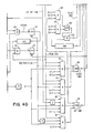
- the switching means represented symbolically in Fig. 2 as a three-position electromechanical switch 16 corresponds to semiconductor switching elements which include gates and flip-flops SW1, SW2, SW3, 48 and 98, Fig. 4B.
- SW1 is a three-input AND gate, one input to which comes directly from the normal message interface 12 through conductor 14, Fig. 2.
- the other two inputs to SW1 are supplied through inverters 26 and 28, Fig. 4B, from two flip-flops respectively designated SW2 and SW3. Therefore, gate SW1 can be its "on” state only when both of the flip-flops SW2 and SW3 are in their "off” or “reset” states.
- switch 16 Fig. 2 in its No.
- Each of the flip-flops designated "FF" in Figs. 4A-4D is of the edge-triggered type, being turned on at the leading edge of the first clock pulse which is supplied to the flip-flop coincidentally with the application of a "1" input pulse to its data (D) terminal.
- D data
- the clock terminals of the various flip-flops and shift registers and the respective sources of clock pulses thereto are omitted from Figs. 4A-4D.
- the flip-flops SW2 and SW3 are self-latching. When either of these flip-flops is turned on, it will remain on until a reset pulse is supplied to its "R" terminal, regardless of any change in the "D" input that may occur during the interim. Referring again to Fig.
- the switch setting is 1, as denoted in box 30, Fig. 3, so that normal message data may pass through the direct connection 14 (Figs. 2, 4A and 4B) from the DTE to the DCE.
- the direct connection 14 As each bit of a normal message stream passes through this connection 14, it also is entered concurrently into the first stage of the shift register X1, from whence it is shifted progressively through the remainder of the delay line afforded by the shift registers X1, X2 and X3.
- the register X1 holds the most recently generated eight bits of the normal message stream, while the register X2 holds the preceding eight bits thereof.
- supervisory apparatus When the supervisory apparatus is ready to transmit a supervisory message, it raises a supervisory request-to-send (S/RTS) signal.
- S/RTS supervisory request-to-send
- the switch control means is continually testing for the presence of the S/RTS signal, as indicated in flowchart box 32, Fig. 3, and when such a signal is detected, it alerts the system to look for the earliest opportunity to place the supervisory message upon the line without curtailing the current normal message. This is accomplished as follows:
- gate 38 passes a satisfaction signal through OR gate 47 to the data (D) terminal of flip-flop SW3, Fig. 4B, turning it on. If idle characters are registered in X1 and X2 when S/RTS comes on, gate 39 then passes a signal through OR gate 47 to flip-flop SW3, turning it on.
- SW3 When SW3 is turned on, it conditions an AND gate 48, Fig. 4B, so that it can pass supervisory message data (S/T X D), when available, from line 49 to the DCE Transmit unit. At the same time, acting through inverter 28, the SW3 signal disables the SW1 gate. The SW3 signal also is applied to an AND gate 50, Fig. 4A. The coincidence of the supervisory request-to-send (S/RTS) signal and the SW3 signal at gate 50 causes the latter to emit a supervisory clear-to-send (S/CTS) signal back to the supervisory equipment, as shown in Fig. 2, thereby initiating transmission of the supervisory message data (S/T X D). Supervisory data now passes from line 49, Figs. 4A and 4B, through the SW3 gate 48 and OR gate 29 to the driver interface 18, Fig. 2, thence through the DCE Transmit unit or modem 20 to the common channel 22.
- S/T X D supervisory message data
- a return of the S/RTS signal to zero level is an indication that the supervisory message has been ended. Usually this does not occur until the trailing flag of the supervisory message has been generated. However, it is possible that S/RTS may drop to zero prematurely due to a malfunction.
- the system must decide whether the switch 16 (Fig. 2) can return immediately from its No. 3 setting to its No. 1 setting or whether it first must assume its intermediate No. 2 setting. The means for making this decision now will be described.
- a timing pulse is generated to denote the duration of the first bit clocking time which coincides with the return of S/RTS to zero.
- this function is performed by the combination of flip-flop 54, inverter 55 and AND gate 56.
- a malfunction could cause the S/RTS signal to drop off prematurely before a complete supervisory message has been transmitted. Under some circumstances this could cause serious problems if no preventive measures were taken. For example, assume that the S/RTS signal falls at an instant when only the first twelve bits FXXXX of the supervisory message (Fig. 1) have been sent and that, by coincidence, the normal message generating means is just then preparing to transmit the first flag of a new normal message after having previously generated a string of idle characters. Ordinarily, when the S/RTS signal goes to zero upon completion of a supervisory message, and the shift registers X1 and X2, Fig. 2, are currently storing idle (L) characters, it could be assumed that the switch setting may change immediately from 3 to 1.
- the 20-bit delay line X4-X5-X6, Figs. 2 and 4C registers the fact that the header of a new supervisory message is being processed whenever the 8-bit shift registers X4 and X6 are concurrently storing flags.
- This information is passed through AND gates 58 and 59, Fig. 4C, and the AND gate 60, Fig. 4D, to a flip-flop 61.
- flip-flop 61 As flip-flop 61 turns on, it sends a signal through a shift register X7 (which functions as a delay line) to an AND gate 62.
- a shift register X7 which functions as a delay line
- flip-flop 64 As flip-flop 64 turns on, it furnishes a reset signal to flip-flop 61 and also produces a "3RD SUPERVISORY FLAG" signal denoting the completion of the supervisory message.
- the length of the delay line X7 is optional, within limits. In the present embodiment X7 is assumed to be 8 bits in length. Its purpose is merely to insure a time separation between the flag which turns on flip-flop 61 and the flag which turns on flip-flop 64.
- a "YES" output from flow-chart box 66 denotes that a complete supervisory message has been generated, as evidenced by the presence of a "third supervisory flag" signal from flip-flop 64, Fig. 4D.
- flip-flop 64 will still be in its off state.
- S/RTS drops to zero (thereby terminating the supervisory message generation) before the trailing flag (that is, the third flag F. Fig. 1) has been generated
- flip-flop 64 will remain off as S/RTS drops to zero. Thereupon the operation will follow the "NO" branch from flowchart box 66.
- the supervisory message has been completed at the time when the S/RTS signal drops to its zero level. Now the system must decide whether the switch setting may change from 3 to 1 immediately or whether it must go first to setting 2 before returning to setting 1.
- Loss of synchronization also may result from a premature termination of the supervisory message due to unwanted failure of the S/RTS signal.
- a sudden return to switch setting 1 under any of these conditions could cause a normal message flag or the byte following it to be truncated, or in some instances it could cause the leading portion of a normal message to become indistinguishable from the trailing portion of a truncated supervisory message.
- the disclosed system has been designed with certain safeguards to insure an orderly return to normal message transmission following the termination of a supervisory message under any of the unfavorable circumstances just described.
- the logical procedure advances to a decision node 74, where it remains until a flag is found in register X2.
- a flag in a register X2 marks a byte synchronization time in the normal message generating process.
- the flag registered in X2 actually was generated one full byte time (eight bit times) ago by the DTE, and it has taken that time to enter register X2 in the delay line X1-X2-X3.
- the byte which had been generated by the DTE most recently is now in register X1, and it may be another flag or a significant data byte (that is a character other than a flag or idle). At this time it is not known what bit sequence now stands in register X3. It is possible that register X2 now contains the only flag registered in the delay line X1-X2-X3.
- supervisory message might have been terminated at a point where two successive flags now must be sent out by the transmitting DCE in order to mark the end of the truncated supervisory message.
- a string of from one to seven zero bits might have passed through switch position 3 while the system was waiting for register X2 to acquire a complete flag bit pattern.
- the switch remains in its setting 2 until the condition of the delay line X1-X2-X3 indicates that no normal message data is passing through it.
- the switch setting is changed from 2 to 1 so that the next normal message (if there is one) may pass directly through switch position 1 to the DCE, bypassing the delay line X1-X2-X3.
- AND gates 82, 84, 86 and 88, Fig. 4D receives among its various inputs and enabling signal from flip-flop SW3, when the switch setting is 3, and a signal from flip-flop 64 (inverted in the case of gate 88) denoting whether or not a third supervisory flag has been detected at the trailing end of the supervisory message.
- the AND gate 84 performs the functions depicted in flowchart boxes 70 and 72, Fig. 3. This gate can be enabled only during the "first bit time", which is contemporaneous with the return of S/RTS to zero. If at this time the shift registers X1 and X2 are holding flags from the DTE, and the final supervisory flag has just been sent, this means that the final supervisory flag was generated in synchronism with the normal message flags generated by the DTE and that, as yet, no significant normal message data has been generated by the DTE. Under these conditions it is safe to return the switch setting immediately from 3 to 1. Accordingly, the AND gate 84 sends a signal through OR gate 90 to reset the flip-flop SW3, Fig. 4B, .
- the trailing supervisory flag can, if necessary, serve also as the leading flag of a new normal message, if one is not otherwise provided. If the necessary conditions just described are not met, AND gate 84 then cannot be activated to reset SW3, and a different action must be taken.
- Gate 86 performs the function denoted by the "NO" branch from flowchart box 70, Fig. 3, and the "YES” branch from flow- chart box 74. No significant action occurs until a flag appears in shift register X2. Then the AND gate 86 passes a signal through an OR gate 92 for setting the flip-flop SW2. As SW2 goes on, several actions occur. First, the combination of an inverter 94 and AND gate 95, Fig.
- flip-flop SW2 When flip-flop SW2 was turned on, it also caused an enabling signal to pass through a 16-bit delay line X8, Fig. 4D (corresponding to flowchart box 78, Fig. 3) and be applied to one input terminal of an AND gate 100.
- Two AND gates 102 and 104 are arranged so that when the current normal message ends, or if there is no normal message, the appearance of an "all-flags" or "all-idles" condition in the shift registers X1, X2 and X3 will apply a signal through an OR gate 106 to the AND gate 100. If this signal is presented to gate 100 more than sixteen bit times after flip-flop SW2 was turned on, gate 100 then passes a reset signal to flip-flop SW2. This corresponds to the action depicted by flowchart boxes 80 and 30. As flip-flop SW2 turns off, it disables the AND gate 98 and restores the AND gate SW1 to its normal conductive state.
- a supervisory message removal apparatus as shown in Figs. 5-7 for withdrawing supervisory messages from the incoming data stream at a utilization point which precedes the data terminal equipment (DTE) to which the incoming normal messages are being directed.
- the arrangement is such that no significant portion of a received supervisory message is permitted to enter the DTE, and the entire supervisory message is routed to the supervisory equipment (not shown).
- the message removal apparatus of Figs. 5-7 and the message insertion aoparatus of Figs. 2-4D are at two different locations in a data communication network. In practice, however, each location may have both types of apparatus. It should be understood also that a supervisory message and a normal message may be sent out from a given location on the same channel to different ultimate destinations. Likewise, a given location in the network may receive a normal message and a supervisory message over the same channel from different originating locations. In all of these cases the supervisory message insertion and removal procedures will be substantially as described herein.
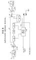
- FIG. 5 schematically illustrates an apparatus for performing that function.
- DCE receiving data communication equipment
- SW two-position switch
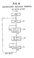
- Fig. 6 is a flowchart of the supervisory message removal procedure.
- the switch unit 118 (Fig. 5) normally is in setting 1, where it serves to pass the received message data from the receiving DCE and interface 114 to the driving interface 122 and DTE unit 124.
- the switch unit 118 (Fig. 5) normally is in setting 1, where it serves to pass the received message data from the receiving DCE and interface 114 to the driving interface 122 and DTE unit 124.
- the switch unit 118 Fig. 5
- the switch unit 118 Fig. 5
- the switch unit 118 (Fig. 5) normally is in setting 1, where it serves to pass the received message data from the receiving DCE and interface 114 to the driving interface 122 and DTE unit 124.
- the test for identifying a supervisory message is satisfied, as denoted by the YES branch from the flowchart box 126.
- this causes a switch control unit 130, Fig.
- the switch 118 is reset to 1 so that the next byte of data which passes through the receiving interface 114 is routed through the conductor 116 and switch position 1 to the receiving DTE 124, as represented by the flow- chart box 132, Fig. 6.
- the flag which was generated by the register X12 and which passed through switch position 2 to the DTE just before the switch 118 returned to its position 1 now may serve as the leading flag of the normal message passing through switch position 1.
- Fig. 7 shows exemplary logic circuitry for executing the functions depicted in the flow- chart of Fig. 6.
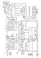
- the delay line X9-X10-X11 consists of two eight-bit shift registers X9 and X11 linked by an intervening 4-bit shift register X10.
- AND gates 134 and 136 respectively furnish satisfaction signals when flags are present in registers X9 and X11. If flags are simultaneously present in registers X9 and X11, coincident enabling signals then are applied to an AND gate 138, which turns a flip-flop 140 on to indicate that a supervisory message header consequence FXXXXF has been detected in the incoming data stream.
- Flip-flop 140 has a certain response time during which its output voltage is still zero while an input voltage is being applied to its D terminal by AND gate 138. This input voltage also is applied to an AND gate 142. The other input to gate 142 is supplied by flip-flop 140 through inverter 144. During the short response period of flip-flop 140, the AND gate 142 therefore receives coincident enabling inputs from gate 138 and inverter 144, causing AND gate 142 to emit a brief pulse to a register loading circuit 146, causing a flag bit pattern to be entered into the recirculating shift register X12 in a desired time relationship with the flag that is present in register X9 at this instant. The purpose of such an arrangement will be explained presently.
- flip-flop 140 When flip-flop 140 turns on, it also applies enabling signals to a flip-flop 147 and an AND gate SW2 (corresponding to switch setting 2). Through an inverter 148, it applies a disabling signal to AND gate SW1, which corresponds to switch setting 1.
- gate SW2 When gate SW2 is enabled, it causes flags generated by the recirculating register X12 to be sent continuously through OR gate 150 to the DTE. Such flags take the place of any supervisory message bytes that otherwise would pass directly through conductor 116 and gate SW1 (now disabled) to the DTE. The supervisory message meanwhile is routed through delay line X9-X10-X11 to the supervisory equipment.
- flip-flop 147 As flip-flop 147 is turned on, it furnishes to the supervisory equipment a signal that enables this equipment to receive the supervisory message train, which now is commencing to exit from shift register X11. Concurrently therewith, the flip-flop 140 supplies a disabling signal through an inverter 152 to gate 138, and through a shift register X13 it supplies an enabling signal to an AND gate 154. The shift register X13 delays application of this enabling signal to gate 154 for a limited time, permitting the present flag to be cleared out of register X9 before conditioning gate 154 to sense the arrival in register X9 of a subsequent flag at the trailing end of the supervisory message. Every received supervisory message, whether complete or truncated, will have a trailing flag.
- register X9 As this flag enters register X9, the coincident input signals at gate 154 enable this gate to pass a reset signal directly to flip-flop 140 and, through a shift register X14, to flip-flop 147.
- the reset delay afforded by register X14 will allow all of the supervisory message bits now standing in the delay line X9-X10-X11 to pass into the supervisory equipment before flip-flop 147 goes off and terminates the signal which had enabled the supervisory equipment to receive message data.
- flip-flop 140 As flip-flop 140 goes off, it terminates the enabling signal to gate SW2, restores the enabling signal to gate SW1, removes the disabling signal from gate 138, and after a delay afforded by a shift register X13, removes the enabling signal from gate 154.
- gate SW2 As gate SW2 is disabled and gate SW1 is enabled, received data bits now may pass through conductor 116 and gate SW1 directly to the DTE.
- the trailing flag of the terminated supervisory message also had been serving as the leading flag of a new normal message
- the final flag that passed from the re- circulatinq register X12 through gate SW2 before gate SW2 was disabled now serves as the leading flag of the normal message passing through gate SW1.
- switch or "switch means” as employed herein, or the representation of an element as an electromechanically operated switch in the drawings, should be broadly construed to mean any appropriate circuit closing or opening device or a coupling means of any other type that is suited to perform the required function of establishing or interrupting a specific operative connection at the place in the circuitry where it is located.
- the "setting” or position of a switch is simply its current state, or more particularly, the present condition of the electrical circuitry which is specifically controlled by that switch. Different settings or positions of a given switch may refer to different circuit-controlling elements. For instance, the symbolic switch 16 in Fig. 2 has settings 1, 2 and 3 which actually correspond to the following elements shown in Fig. 4B:
Description
- This invention relates to digital data communication systems, teleprocessing networks and the like, and in particular it relates to multiplexing schemes for introducing supervisory messages into data streams containing normal message transmissions.
- As used herein, the term "supervisory message" applies broadly to any information which is utilized for monitoring and/or controlling the operations of equipments in a communication system, as distinguished from information which is utilized for normal data processing purposes without regard to the manner in which the communication equipment is functioning or malfunctioning. Supervisory messages commonly include diagnostic information sent from remote equipments to a central station and commands sent from the central station to the remote equipments in response thereto.
- The term "digital" is used herein to denote information which is communicated in the form of discrete pulses, and it includes digitized analog signals as well as coded binary data. It has been found costly and otherwise undesirable to provide special modems or special separate communication channels for handling supervisory messages. It is preferable that supervisory messages be communicated by facilities which are no more expensive and require no greater frequency bandwidth than the facilities that otherwise would be needed to handle normal message traffic in the complete absence of any supervisory messages. One way to accomplish this objective is to employ time division multiplexing whereby the time during which a communication channel is used will be divided between time intervals wherein normal messages may be sent and other time intervals that are utilized only for supervisory messages. Since the normal messages rarely use 100 percent of the time available, supervisory messages may be inserted whenever interruptions in the normal message transmissions occur. This practice does not expand the bandwidth of the communication channel nor does it affect the complexity of the normal communication protocols by the act of accommodating the supervisory messages.
- In one form of time division multiplexing that has been known heretofore, certain regularly occurring time slices or digit spaces are reserved exclusively for the digits of supervisory messages, regardless of whether or not there are any supervisory messages to be transmitted. This practice of allocating predetermined fixed time slices to supervisory messages can be wasteful when little or no supervisory. data is to be sent, and insufficient when a great deal of it is to be sent. It is just as desirable to use time economically as it is to minimize the cost of the equipment which is being used. Supervisory messages are likely to occur in random fashion at unpredictable times, not at regular intervals, and it would be inefficient to reserve regularly occurring time intervals for handling such messages, because often these intervals would not be utilized for any useful purpose. Furthermore, it is not usually necessary for the supervisory messages to preempt the channel immediately. In most, if not all, instances they can await the inevitable gaps in the normal message flow.
- Various arrangements for transmitting a second kind of information during gaps of a first kind of information are already known, e.g., from Swiss Patents 360 095 and 434 378 and from
British Patent 1 021 927. -
British Patent 1 021 927 discloses a system in which normally coded speech is transmitted but when a pause is recognized by detecting circuitry, characters from a data store are transmitted. When speech is detected again, transmission of coded speech is resumed after sending one more data character and a PCM resume code. During this time one or two speech samples may be lost which is not critical for speech transmission but is not acceptable when the normally transmitted information is data. - Above mentioned Swiss Patent 434 378 also shows apparatus by which data from a storage can be transmitted during pauses in speech. A magnetic drum is inserted as delay unit in the speech path. Detecting, timing and control circuitry causes a switchover from the speech path to the output of a data storage only if a speech pause is detected whose duration exceeds a given minimum. This arrangement has the disadvantage that the first kind of information (the speed signal in this case) is always delayed. Furthermore, only pauses exceeding a minimum duration are utilized.
- It is an object of the present invention to enable the insertion of messages of a second kind, in particular supervisory messages, into gaps left between messages of a first kind, i.e. normal messages, with a minimum in delay on one hand and an optimum utilization on the other hand, but also with an exact timing and clear limitation at the transitions, so that given rules for formats or delimiters of messages can be adhered to.
- The invention for achieving this object is defined in
claim 1. - It has the advantage that it allows to introduce a delay in the normal message stream only when necessary, but to eliminate this delay as soon as possible. The selectively insertable delay serves a two-fold purpose. It allows, when not inserted, to buffer characters for recognition which were already transmitted without delay, but when inserted it holds the starting characters of a message which are to be transmitted, until some switching or transition procedure is completed. A switching-over to the supervisory character generator, which may later necessitate insertion of a delay is only effected when necessary, i.e. when a request exists. The message status detecting circuitry allows exact timing of the switchover or exact insertion of a switchover character in dependence of the present positional status of the normal message stream which per se is timed independently of the multiplexing arrangement. The multiplexing arrangement is also particularly useful for message streams in which the gaps may be either filled by idle characters or by sequences of delimiting flags which on the other hand may denote the start or the end of a message.
- The technique disclosed herein can even be retrofitted to existing systems without affecting the DTE's therein.
- The detection of a gap in normal message transmission may be accomplished in any convenient way according to the particular environment in which the invention is being used. For example, if synchronous data link control (SDLC) is being utilized for the normal message transmission, the occurrence of a gap between normal messages will be signaled by the transmission of a distinctive eight-bit character pattern called a "flag" following any eight-bit pattern or byte which is neither a flag nor an "idle" character. Under these circumstances the flag denotes the end of a normal message, and it is assumed that a sufficient time interval will elapse before the beginning of the next normal message to permit the insertion of a supervisory message, if one is awaiting transmission at that time.
- The insertion of the supervisory message commences as soon as the trailing flat of the normal message has been sent. If the assumption is incorrect, and a new normal message is started while the transmission of the supervisory message is still in progress (as signaled by a flag followed by a character which is neither a flag nor an idle), the invention then makes provision for immediately terminating the incomplete supervisory message with a distinctive ending sequence such as a flag so that normal message transmission can be resumed without significant delay.
- As can be appreciated, the invention is based upon the concept that supervisory messages will be held for transmission during randomly occurring idle intervals in the normal message transmission, so that the introduction of supervisory messages will not significantly extend the time required for transmitting the normal messages and will not in any significant way interfere with the normal message transmission.
- The foregoing and other objects, features and advantages of the invention will be apparent from the following more particular description of a preferred embodiment of the invention, as illustrated in the accompanying drawings.
-
- Fig. 1 is a bit sequence representation showing a preferred supervisory message format that can be conveniently employed in a data communication system embodying the invention.
- Fig. 2 is a general block diagram of an apparatus designed for use at a transmitting location in a data communication system for inserting supervisory messages into gaps that occur in the normal message stream, according to the invention.
- Fig. 3 is a flowchart of the supervisory message insertion process.
- Figs. 4A to 4D, when arranged according to Fig. 4, constitute a more detailed logic diagram of the supervisory message insertion apparatus shown in Fig. 2.
- Fig. 5 is a block diagram of an apparatus for withdrawing or removing supervisory messages from the normal message stream at a receiving location, in accordance with the invention.
- Fig. 6 is a flow-chart of the supervisory message removal process.
- Fig. 7 is a more detailed logic diagram of the supervisory message removal apparatus shown in Fig. 5.
- The invention is disclosed herein as being embodied in a data communication system which utilizes synchronous data link control (SDLC). It should be understood, however, that the invention is not limited to SDLC systems and is capable of being applied to other digital communication systems, such as binary synchronous communication (BSC) systems.
- In a system using the SDLC discipline, the normal message format is indicated below:
- F A C D FCS F, where
- F=Flag=01 111110
- A=Address byte
- C=Control byte
- D=Data field
- FCS=Frame check sequence
- As indicated above, a normal SDLC message commences with a flag (F) and terminates with another flag. Each flag F is an eight-bit byte consisting of an initial 0 followed by six consecutive 's and a final 0. The initial or leading flag of the message is followed by the address (A) and control (C) bytes, which in turn are followed by a data (D) field that does not have a fixed length but typically contains 100 bits. The frame check sequence (FCS) contains 16 bits (two bytes). It should be noted that even if the message had a data field of zero length, the leading and trailing flags therein still would be separated by four bytes (A byte, C byte and two FCS bytes). Hence, in a normal SDLC message the minimum separation between flags is four bytes (32 bits). Any message that contains two flags separated by a lesser number of bits can readily be recognized as something other than a normal message, presumably a supervisory message.
- A gap between normal SDLC messages may be filled with flags F, each represented by a
bit string 01111110, or by idle characters L, each represented by a string of eight "1" bits, 11111111. The choice is optional, according to whether the sending terminal is endeavoring to hold the channel or is willing to release it to another terminal in the network. - In a communication system wherein normal messages and supervisory messages may be transmitted in interspersed relationship over a common line or channel, the supervisory messages should have a format which is sufficiently distinct from the normal message format so that these supervisory messages can readily be detected and segregated from the normal messages at an appropriate utilization point in advance of the normal message receiver. On the other hand, the supervisory and normal message formats should not differ so much from each other as to introduce special communication problems which would adversely affect the operation of the conventional data terminal equipment or require a basic redesign of the system. The foregoing requirements can be met by choosing a supervisory message format which resembles a normal message format except that in the supervisory message an extra flag is inserted at a position which is less than four bytes (32 bits) from the leading flag of this message.
- In the preferred supervisory message format shown in Fig. 1, an extra flag F* is inserted after the first four bits of the A byte which follows the leading flag F. Thus, the inserted flag F* is separated from the leading flag F by a number of bit positions which is less than four bytes and which moreover is not an integer multiple of a byte. This insures that a supervisory message can readily by identified as such at the receiver, inasmuch as a normal message would have at least four bytes between flags. It also insures that in case of errors on the line, a string of incorrectly transmitted flags will not be confused with the distinctive bit sequence or "header" which marks the beginning of a supervisory message, because it is highly unlikely that two nonadjacent flags in a normal message stream would be separated by a number of bits which is not an integer multiple of a byte, regardless of line errors. It should be understood, of course, that the choice of a four-bit separation between F and F* in Fig. 1 is meant to be exemplary and that other suitable spacings which are not byte integers could be selected as well. The means for generating supervisory messages and other supervisory signals will not be disclosed in detail herein. Such instrumentalities are of conventional design or can readily be adapted therefrom.
- In the disclosed system, wherein normal messages are given priority over supervisory messages, a supervisory message may be abruptly terminated before its completion (i.e., before its third flag is generated) if this is necessary in order to clear the channel for a normal message transmission. A supervisory message also may become truncated due to some malfunction of the equipment. In either event the system will automatically provide the truncated supervisory message with a distinctive ending bit sequence in order to demarcate it from a succeeding normal message.
- Fig. 2 is a conceptual block diagram which schematically illustrates the principle of supervisory message insertion as contemplated by the invention. The "DTE Transmit"
unit 10 is conventional data terminal equipment for generating the normal messages which are to be transmitted. The data to be transmitted from unit 10 (Tx Data) is sent through an Electronic Industries Association standard data receiving (EIA RX)interface 12 to two alternative paths, one of which is adirect connection 14 toposition 1 of a three-position switch (SW)unit 16. The other path for the T. Data extends through a series of three eight-bit shift registers X1, X2 and X3 to position 2 of theswitch unit 16. Although theswitch 16 is represented for convenience in Fig. 2 as an electromechanical unit, it should be understood that in practice such switching functions are performed by non- moving electronic elements, as described hereinafter. The term "switch position" or "switch setting" therefore should be understood broadly as meaning the electrical connections established by the switch in its current state. - In its
position 1, switch 16 passes normal messages (TX Data) from theDTE interface 12 through an Electronic Industries Association standard driving (EIA D/R)interface 18 to the DCE (data communication equipment)transmitter 20, otherwise known simply as a "modem". As each bit of normal message data passes throughconductor 14 to switchposition 1, it concurrently is entered also into the first cell of the eight-bit shift register X1, Fig. 2 from whence it progresses through the series of eight-bit shift registers X1, X2 and X3, which together constitute a three-byte delay line. The exit terminal of register X3 is connected to position 2 ofswitch 16. The functions of registers X1, X2 and X3 will be explained presently. The operations of these shift registers are timed by clock pulses supplied thereto by a suitable source (not shown). - After passing through
switch 16,interface 18 andmodem 20, the message is transmitted over the line orchannel 22 to the receiving location. Thechannel 22 is used for communicating both normal messages and supervisory messages. When a supervisory message is being transmitted, switch 16 is inposition 3. Supervisory data to be transmitted (S/Tx D) passes from a source such as a conventional type of diagnostic card (not shown) throughswitch position 3,driver interface 18 andmodem 20 to thecommon channel 22. - The setting of
switch 16 is controlled by aswitch control unit 24, Fig. 2, which normally is inposition 1 but may in some instances assumeposition Unit 24 may function in response to a supervisory request-to-send (S/RTS) signal, normal message data stored in the delay line X1-X2-X3 and/or supervisory message data stored in a 20-bit delay line comprising two 8-bit shift registers X4 and X6 and an intervening 4-bit shift register X5. Inposition 1switch 16 passes normal message data directly from theDTE unit 10 tomodem 20. For passing supervisory message data, switch 16 assumesposition 3. Occasionally a supervisory message may be ended prematurely as explained hereinabove. In this event, switch 16 changes its setting from 3 to 2, abruptly terminating the supervisory message transmission with a flag generated especially for that purpose and commencing the normal message transmission with information initially contained in the delay line X1-X2-X3. Ultimately switch 16 returns toposition 1. - When the setting of
switch 16 is changed as described above, a temporary loss of synchronization may occur due to the standard "zero stuffing" procedure which is employed in SDLC encoders. It is customary to insert a "0" after each string of five consecutive 1's that may occur between the final "0" of a leading flag and the first "0" of a trailing flag in a SDLC message. This prevents the inadvertent occurrence of abit sequence 01111110 which simulates a flat at a place in the transmitted message where no flag was intended. The "stuffed zeros" are disregarded when the received message is decoded. However, their presence in an encoded message tends to complicate the recovery of synchronization after a change of switch setting. In the present system this problem is adequately handled by means described hereinafter. - Reference now is made to Fig. 3, which shows the flow-chart for the supervisory message insertion process that is performed by the apparatus shown schematically in Fig. 2. It is optional whether the functions depicted in this flowchart are implemented in software (microprogramming) or are carried out by hardwired logic circuitry such as that shown in Figs. 4A to 4D. For present purposes it is assumed that the supervisory message insertion procedure is embodied in the circuitry shown, because in practice it is preferable to use hardware rather than software for implementing the switch control functions. However, this does not necessarily imply that in a commercial implementation one must use the specific form of logic circuitry shown herein. For reasons of economy it may be desirable to employ standard chip circuitry, which contains more elements than are actually needed, utilizing only those portions thereof which correspond functionally to the circuitry shown herein.
- The switching means represented symbolically in Fig. 2 as a three-position
electromechanical switch 16 corresponds to semiconductor switching elements which include gates and flip-flops SW1, SW2, SW3, 48 and 98, Fig. 4B. SW1 is a three-input AND gate, one input to which comes directly from thenormal message interface 12 throughconductor 14, Fig. 2. The other two inputs to SW1 are supplied throughinverters conductor 14 through ORgate 29, Fig. 4B, to theoutgoing message interface 18, Fig. 2. When the flip-flop SW2, Fig. 4B, is turned on, this corresponds to the condition ofswitch 16 when it is in its No. 2 setting. Similarly, when flip-flop SW3 is turned on, this has the same effect as placingswitch 16 in its No. 3 position. Normally both of the flip-flops SW2 and SW3 are off, and by default this puts gate SW1 in its "on" condition. Only one of the switching elements SW1, SW2 and SW3 may be on at any one time. - Each of the flip-flops designated "FF" in Figs. 4A-4D is of the edge-triggered type, being turned on at the leading edge of the first clock pulse which is supplied to the flip-flop coincidentally with the application of a "1" input pulse to its data (D) terminal. To avoid unduly complicating the drawing, the clock terminals of the various flip-flops and shift registers and the respective sources of clock pulses thereto are omitted from Figs. 4A-4D. The flip-flops SW2 and SW3 are self-latching. When either of these flip-flops is turned on, it will remain on until a reset pulse is supplied to its "R" terminal, regardless of any change in the "D" input that may occur during the interim. Referring again to Fig. 3, a statement such as SW==1, SW=2, or SW=3 in a flow-charge box means that the respective switch element SW1, SW2 or SW3, Fig. 4B, is currently in its "on" state. Initially the switch setting is 1, as denoted in
box 30, Fig. 3, so that normal message data may pass through the direct connection 14 (Figs. 2, 4A and 4B) from the DTE to the DCE. As each bit of a normal message stream passes through thisconnection 14, it also is entered concurrently into the first stage of the shift register X1, from whence it is shifted progressively through the remainder of the delay line afforded by the shift registers X1, X2 and X3. The register X1 holds the most recently generated eight bits of the normal message stream, while the register X2 holds the preceding eight bits thereof. - When the supervisory apparatus is ready to transmit a supervisory message, it raises a supervisory request-to-send (S/RTS) signal. The switch control means is continually testing for the presence of the S/RTS signal, as indicated in
flowchart box 32, Fig. 3, and when such a signal is detected, it alerts the system to look for the earliest opportunity to place the supervisory message upon the line without curtailing the current normal message. This is accomplished as follows: - The contents of the registers X1 and X2 are continuously monitored to detect a condition signifying either the end of a normal message, if one currently is being transmitted, or an idle condition of the line or channel if no normal message is being transmitted. In the SDLC procedure the end of a normal message is signaled when register X1 holds a flag byte and register X2 concurrently is storing a byte that is neither a flag nor an idle character (usually the second byte of the frame check sequence FCS). If such a condition is detected at a time when a supervisory request-to-send (S/RTS) signal is being emitted by the supervisory equipment, as denoted by
flowchart box 34, Fig. 3, the switch setting is changed from 1 to 3, as shown atflowchart box 36, thereby putting the apparatus of Fig. 2 into a condition to transmit a supervisory message during the time interval which follows the completion of the normal message transmission and prior to the beginning of the next normal message. If the normal message generating means is idle, registers X1 and X2 then store idle (L) characters, and detection of this condition (box 37, Fig. 3) causes the switch setting to change from 1 to 3 (box 36). - In the circuitry of Fig. 4A, the functions depicted by the
flowchart boxes gates 38 and 39. One input to each of these gates is the S/RTS signal. Another input to gate 38 is supplied by an ANDgate 40 associated with shift register X1. Whenever a flat bit pattern is stored in register X1, thegate 40 supplies a satisfaction signal (XI =F) to the AND gate 38. Another ANDgate 41 associated with register X1 finishes a satisfaction signal (X1=L) to ANDgate 39 if X1 is storing an idle character. The ANDgates gate 42 furnishes a satisfaction signal (X2=F) to aninverter 45 when X2 registers a flag, andgate 44 furnishes a satisfaction signal (X2=L) toinverter 46 and ANDgate 39 when X2 registers an idle. If the byte currently registered in X2 is neither a flag nor an idle, then the zero outputs fromgates inverters gate 40 is suppling to gate 38 a flag signal from register X1, and also while a S/RTS signal is being furnished to gate 38 by the supervisory equipment, then gate 38 passes a satisfaction signal throughOR gate 47 to the data (D) terminal of flip-flop SW3, Fig. 4B, turning it on. If idle characters are registered in X1 and X2 when S/RTS comes on,gate 39 then passes a signal throughOR gate 47 to flip-flop SW3, turning it on. - When SW3 is turned on, it conditions an AND
gate 48, Fig. 4B, so that it can pass supervisory message data (S/TXD), when available, fromline 49 to the DCE Transmit unit. At the same time, acting throughinverter 28, the SW3 signal disables the SW1 gate. The SW3 signal also is applied to an ANDgate 50, Fig. 4A. The coincidence of the supervisory request-to-send (S/RTS) signal and the SW3 signal atgate 50 causes the latter to emit a supervisory clear-to-send (S/CTS) signal back to the supervisory equipment, as shown in Fig. 2, thereby initiating transmission of the supervisory message data (S/TXD). Supervisory data now passes fromline 49, Figs. 4A and 4B, through theSW3 gate 48 andOR gate 29 to thedriver interface 18, Fig. 2, thence through the DCE Transmit unit ormodem 20 to thecommon channel 22. - Ordinarily one would not expect another normal message to be generated soon after the preceding normal message has ended. Usually there is a sufficient gap between normal messages to permit the transmission of at least one supervisory message, if such a message needs to be transmitted at that time. Supervisory message bits can be transmitted as long as flip-flop SW3 is on (switch position SW=3). Assuming no malfunction, the switch remains in position 3 (flip-flop SW3 on) so long as S/RTS=1 and no new normal message has been initiated, as shown by the repetitive loop including the "No" flow lines from the
boxes - A return of the S/RTS signal to zero level is an indication that the supervisory message has been ended. Usually this does not occur until the trailing flag of the supervisory message has been generated. However, it is possible that S/RTS may drop to zero prematurely due to a malfunction. When S/RTS returns to zero, the system must decide whether the switch 16 (Fig. 2) can return immediately from its No. 3 setting to its No. 1 setting or whether it first must assume its intermediate No. 2 setting. The means for making this decision now will be described.
- A timing pulse is generated to denote the duration of the first bit clocking time which coincides with the return of S/RTS to zero. In the circuitry of Fig. 4A this function is performed by the combination of flip-
flop 54,inverter 55 and ANDgate 56. Flip-flop 54 is edge-triggered, but it is not self-latching. It remains on while S/RTS=1, but when S/RTS drops to zero, flip-flop 54 will remain on only for the duration of the current bit period, dropping off at the trailing edge of the current bit clocking pulse. During the short interval while flip-flop 54 is still on, after S/RTS has returned to zero, the ANDgate 56 is receiving coincident "1" inputs from flip-flop 54 and theinverter 55, thus enablinggate 56 momentarily to emit a "1 ST BIT TIME" signal pulse for the duration of that interval. This information is needed under some conditions, as will be explained. - As mentioned hereinabove, a malfunction could cause the S/RTS signal to drop off prematurely before a complete supervisory message has been transmitted. Under some circumstances this could cause serious problems if no preventive measures were taken. For example, assume that the S/RTS signal falls at an instant when only the first twelve bits FXXXX of the supervisory message (Fig. 1) have been sent and that, by coincidence, the normal message generating means is just then preparing to transmit the first flag of a new normal message after having previously generated a string of idle characters. Ordinarily, when the S/RTS signal goes to zero upon completion of a supervisory message, and the shift registers X1 and X2, Fig. 2, are currently storing idle (L) characters, it could be assumed that the switch setting may change immediately from 3 to 1. In the present case this must not be permitted to occur, however, because the leading flag of the new normal message then would immediately follow the 12-bit sequence FXXXX of the truncated supervisory message, thereby making it appear that the normal message is part of a supervisory message inasmuch as the combined bit strings would then simulate a supervisory message format (Fig. 1).
- Another problem of this kind could occur if the S/RTS signal were interrupted just after the leading 20 bits FXXXXF of the supervisory message had been sent and at a time when the delay line X1-X2-X3 is holding a string of flags, the most recent of which (in register X1) is the leading flag of a new normal message. Here again, some action must be taken to prevent the switch setting from being changed immediately from 3 to 1, as otherwise would happen after the termination of a supervisory message if registers X1 and X2 are then storing flags. Otherwise the part of the normal message following the first flag will seem to be that part of a supervisory message which follows the second flag therein. The present system avoids problems of this kind by preventing a change of switch setting directly from 3 to 1 whenever the S/RTS signal drops to zero before the final flag of the supervisory message has been generated.
- The 20-bit delay line X4-X5-X6, Figs. 2 and 4C; registers the fact that the header of a new supervisory message is being processed whenever the 8-bit shift registers X4 and X6 are concurrently storing flags. This information is passed through AND
gates gate 60, Fig. 4D, to a flip-flop 61. As flip-flop 61 turns on, it sends a signal through a shift register X7 (which functions as a delay line) to an ANDgate 62. Thus, the flip-flop 61, Fig. 4D, remembers that the opening sequence FXXXXF of the supervisory message has been generated and, after a delay interval, supplies this information continuously to ANDgate 62. Subsequently, when the trailing flag of the supervisory message has been sent, the shift register X4 momentarily stores a flag bit pattern, which is detected by ANDgate 58. This information also is supplied to ANDgate 62, which now passes to a flip-flop 64 a signal indicating that the circuitry has detected a bit sequence FXXXXF followed at a later time by a trailing flag F, showing that a supervisory message was both initiated and completed. As flip-flop 64 turns on, it furnishes a reset signal to flip-flop 61 and also produces a "3RD SUPERVISORY FLAG" signal denoting the completion of the supervisory message. The length of the delay line X7 is optional, within limits. In the present embodiment X7 is assumed to be 8 bits in length. Its purpose is merely to insure a time separation between the flag which turns on flip-flop 61 and the flag which turns on flip-flop 64. - Referring to Fig. 3, a "YES" output from flow-
chart box 66 denotes that a complete supervisory message has been generated, as evidenced by the presence of a "third supervisory flag" signal from flip-flop 64, Fig. 4D. However, if the message has not yet been completed at the time in question, flip-flop 64 will still be in its off state. Hence, if S/RTS drops to zero (thereby terminating the supervisory message generation) before the trailing flag (that is, the third flag F. Fig. 1) has been generated, then flip-flop 64 will remain off as S/RTS drops to zero. Thereupon the operation will follow the "NO" branch fromflowchart box 66. For the time being it will be assumed that the supervisory message has been completed at the time when the S/RTS signal drops to its zero level. Now the system must decide whether the switch setting may change from 3 to 1 immediately or whether it must go first to setting 2 before returning to setting 1. - As shown in
flowchart box 68, Fig. 3, it is safe to return the switch 16 (Fig. 2) immediately from setting 3 to setting 1 if the shift registers are storing idles at the time when the supervisory message is completed. This action is represented by the "YES" branch frombox 68 and involves resetting the flip-flop SW3, Fig. 48, thereby enabling the AND gate SW1 so that it again may pass normal message data directly from the DTE to the DCE. Even though registers X1 and X2 are not currently storing idles, however, there is still a chance that the switch setting may be returned to 1 during the first bit time after S/RTS goes down, provided the registers X1 and X2 at that instant are storing flags. Under these conditions the worst that can happen is that the first significant byte (A) of the normal message passes to the DCE immediately after the trailing flag of the supervisory message has passed through the DCE. This is acceptable, because the trailing flag of any message always may serve as the leading flag of a normal message that immediately follows It. (A supervisory message, however, always should have its own leading flag). Thus, referring toboxes - If neither idles nor flags are present in both of the registers X1 and X2 at the time when S/RTS goes off then even though the supervisory message is complete, it would be inappropriate to return the switch setting immediately from 3 to 1. This condition indicates that the normal message generator (DTE) may be duly supplying flags to the delay line X1-X2-X3, but these flags are not synchronized with the supervisory message flags. Lack of synchronization between normal message flags and supervisory message flags may result from the "zero stuffing" procedure described above, which prevents the random occurrence of spurious flags but also affects the relative timing of the true flags in a message stream. Loss of synchronization also may result from a premature termination of the supervisory message due to unwanted failure of the S/RTS signal. A sudden return to switch setting 1 under any of these conditions could cause a normal message flag or the byte following it to be truncated, or in some instances it could cause the leading portion of a normal message to become indistinguishable from the trailing portion of a truncated supervisory message.
- The disclosed system has been designed with certain safeguards to insure an orderly return to normal message transmission following the termination of a supervisory message under any of the unfavorable circumstances just described. Referring again to Fig. 3, unless the conditions at the time when a supervisory message ends are such as to conform with those represented by the YES branches leading from the
flowchart boxes decision node 74, where it remains until a flag is found in register X2. - The appearance of a flag in a register X2 marks a byte synchronization time in the normal message generating process. The flag registered in X2 actually was generated one full byte time (eight bit times) ago by the DTE, and it has taken that time to enter register X2 in the delay line X1-X2-X3. The byte which had been generated by the DTE most recently is now in register X1, and it may be another flag or a significant data byte (that is a character other than a flag or idle). At this time it is not known what bit sequence now stands in register X3. It is possible that register X2 now contains the only flag registered in the delay line X1-X2-X3. It is possible also that the supervisory message might have been terminated at a point where two successive flags now must be sent out by the transmitting DCE in order to mark the end of the truncated supervisory message. As a further possibility, a string of from one to seven zero bits might have passed through
switch position 3 while the system was waiting for register X2 to acquire a complete flag bit pattern. - In any event, if the conditions are such that the
switch 16, Fig. 2, cannot be returned immediately to itssetting 1 when the supervisory message transmission ends, then it is desirable that the switch assume a setting in which it will cause a minimum of two successive flags to be sent to the DCE before a byte of normal message data other than a flag is sent out. This objective is achieved by placing the switch in itssetting 2 and forcibly loading the register X3 with a flag bit pattern when the register X2 achieves a flag setting, as indicated byflowchart box 76, Fig. 3. Then, by waiting at least 16 bit times for the bits currently stored in registers X2 and X3 to pass throughswitch position 2 to the DCE, as shown inbox 78, assurance is given that at least two flags will precede the arrival of the first byte of normal message data at the DCE and that these flags will be synchronized with the remainder of the normal message. - The switch remains in its
setting 2 until the condition of the delay line X1-X2-X3 indicates that no normal message data is passing through it. When the registers X1, X2 and X3 attain an all-flags or all-idles condition, as indicated inflowchart box 80, then the switch setting is changed from 2 to 1 so that the next normal message (if there is one) may pass directly throughswitch position 1 to the DCE, bypassing the delay line X1-X2-X3. - The functions depicted in the
flowchart boxes gates gate 82 receives an inverted S/RTS signal when S/RTS=0 and coincident inputs from the ANDgates gate 82 to pass a signal throughOR gate 90 for resetting the flip-flop SW3. Since SW2 is off at this time, the resetting of SW3 restores the SW1 gate, Fig. 4B, to its normal conductive state so that it can thereafter pass normal message data, if any, from the DTE to the DCE. This corresponds to the action indicated by theflowchart boxes gate 82 are not fully met, then one of the other ANDgates - The AND
gate 84, Fig. 4D, performs the functions depicted inflowchart boxes gate 84 sends a signal throughOR gate 90 to reset the flip-flop SW3, Fig. 4B, . which has the effect of restoring the AND gate SW1 to its conductive state (flowchart box (30). The trailing supervisory flag can, if necessary, serve also as the leading flag of a new normal message, if one is not otherwise provided. If the necessary conditions just described are not met, ANDgate 84 then cannot be activated to reset SW3, and a different action must be taken. - If the trailing third flag which marks the end of a complete supervisory message has been detected as described above by the time the S/RTS signal drops to zero, but flags or idles are not then present in the shift registers X1 and X2, this indicates that the final supervisory flag was not generated in a synchronously timed relationship with normal message flags. The system now must await the appearance of idles in registers X1 and X2 or a flag in register X2, whichever occurs first. If idles appear in X1 and X2, the switch then may be reset to 1. If a flag appears in register X2, this could be the leading flag of a new normal message. In this event the switch cannot be returned to setting 1 without losing the significant data that now stands in register X1. Even if
register 1 now holds a flag, however, it is too late to return the switch directly from its setting 3 to itssetting 1, because the trailing supervisory flag no longer could serve as the leading flag of the new normal message if one were not already provided. The switch now must assume itssetting 2. - Consideration now will be given to the AND
gate 86, Fig. 4D, which is enabled only after the first bit time has elapsed following the return of S/RTS to zero.Gate 86 performs the function denoted by the "NO" branch fromflowchart box 70, Fig. 3, and the "YES" branch from flow-chart box 74. No significant action occurs until a flag appears in shift register X2. Then the ANDgate 86 passes a signal through anOR gate 92 for setting the flip-flop SW2. As SW2 goes on, several actions occur. First, the combination of aninverter 94 and ANDgate 95, Fig. 4B, creates a very short pulse during the brief interval between the instant when a "Set SW2" signal is applied to flip-flop SW3 and the instant when SW3 changes its state in response thereto. This short pulse acts throughOR gate 90 to reset the flip-flop SW3. It also is applied momentarily to aflag loading circuit 96 for causing a flag bit pattern to be forcibly entered into shift register X3, Fig. 4B, whencircuit 96 is energized. This action places a flag in portion X3 of the delay line X1-X2-X3 immediately preceding the flag that now stands in register X2. As another consequence of activating the flip-flop SW2, an enabling signal is supplied by SW2 to an ANDgate 98, Fig. 4B, which corresponds to switch setting 2, while at the same time a disabling signal is applied throughinverter 26 to AND gate SW1. Thus, flip-flop SW2 is turned on so that ANDgate 98 is now enabled to pass data from the exit end of the delay line X1-X2-X3 to the DCE. The action described above with reference to the flow-chart boxes gate 98 to the DCE. - When flip-flop SW2 was turned on, it also caused an enabling signal to pass through a 16-bit delay line X8, Fig. 4D (corresponding to
flowchart box 78, Fig. 3) and be applied to one input terminal of an ANDgate 100. Two ANDgates gate 106 to the ANDgate 100. If this signal is presented togate 100 more than sixteen bit times after flip-flop SW2 was turned on,gate 100 then passes a reset signal to flip-flop SW2. This corresponds to the action depicted byflowchart boxes gate 98 and restores the AND gate SW1 to its normal conductive state. - In the event that the S/RTS signal returns to zero before the trailing third supervisory flag has been generated, the switch must not be permitted to return immediately from setting 3 to setting 1, for the reasons explained hereinabove. In a worst-case situation, it is possible that the interruption of the supervisory message may occur even before the intermediate flag F* (Fig. 1) has been generated. To insure that the truncated supervisory message will be followed by at least two consecutive flags, the AND
gate 88, Fig. 4D, defers action until a flag appears in register X2; whereupongate 88 then sends a "Set SW2" signal to flip-flop SW2 throughOR gate 92. This results in loading a flag into register X3, followed by the transmission of the two flags from X3 and X2 to the DCE (flow-chart boxes - Thus far it has been assumed that the supervisory request-to-send (S/RTS) signal goes to zero before the DTE starts to generate any significant normal message data (i.e., data other than flags or idles), so that there is no time overlap between the significant leading portion of the new normal message generated by the DTE and the significant trailing portion of the supervisory message generated by the supervisory apparatus. Occasionally, however, the gap between two normal messages may not be sufficient to accommodate a whole supervisory message, and it then becomes necessary to truncate the supervisory message when the new normal message begins. Thfs function (corresponding to the YES branch from
flowchart box 53, Fig. 3) is performed by an ANDgate 110, Fig. 4C, which receives inputs from flip-flop SW3 and ANDgate 42 along with inverted inputs from ANDgates gate 48, Fig. 4B) at a time when the DTE starts to generate a new normal message. This new message cannot pass through gate SW1 at this time, but it can enter the delay line X1-X2-X3. When the leading flag of the normal message appears in register X2, followed by the first byte of non-flag message data in register X1, the conditions are met for switching from setting 3 to setting 2 (flip-flop SW3 turned off; flip-flop SW2 turned on, as ANDgate 110 produces a "Set SW2" signal). A flag is loaded into register X3, and the two flags in X2 and X3 then pass through switch position 2 (AND gate 98), followed by the first significant byte of the normal message. - At the message receiving location there is provided a supervisory message removal apparatus as shown in Figs. 5-7 for withdrawing supervisory messages from the incoming data stream at a utilization point which precedes the data terminal equipment (DTE) to which the incoming normal messages are being directed. The arrangement is such that no significant portion of a received supervisory message is permitted to enter the DTE, and the entire supervisory message is routed to the supervisory equipment (not shown).
- It is assumed in the present description that the message removal apparatus of Figs. 5-7 and the message insertion aoparatus of Figs. 2-4D are at two different locations in a data communication network. In practice, however, each location may have both types of apparatus. It should be understood also that a supervisory message and a normal message may be sent out from a given location on the same channel to different ultimate destinations. Likewise, a given location in the network may receive a normal message and a supervisory message over the same channel from different originating locations. In all of these cases the supervisory message insertion and removal procedures will be substantially as described herein.
- At the receiving location it is necessary that an incoming supervisory message be identified as such and removed from
channel 22 before any significant part of this message can enter the DTE. Fig. 5 schematically illustrates an apparatus for performing that function. As each message, whether normal or supervisory, passes through the receiving data communication equipment (DCE) ormodem 112 and thence through the receivinginterface 114, it is applied through a conductor 116 toterminal 1 of a two-position switch (SW)unit 118 and also to a delay line comprising a series of shift registers X9, X10 and X11. The registers X9 and X11 each have an eight-bit length, and the intervening register X10 has a four-bit length. Hence, when the header sequence FXXXXF of a supervisory message is present in the delay line X9-X10-X11, flags appear simultaneously in registers X9 and X11. This is a signal for commencing the removal of a supervisory message from the incoming data stream. - Fig. 6 is a flowchart of the supervisory message removal procedure. As denoted by
box 120, the switch unit 118 (Fig. 5) normally is in setting 1, where it serves to pass the received message data from the receiving DCE andinterface 114 to the drivinginterface 122 andDTE unit 124. However, when the leading and intermediate flags of a supervisory message concurrently are present in registers X9 and X11, the test for identifying a supervisory message is satisfied, as denoted by the YES branch from theflowchart box 126. As indicated by flow-chart box 128, this causes aswitch control unit 130, Fig. 5, to change the setting ofswitch 118 from 1 to 2 and simultaneously load a flag bit pattern into an eight-bit shift register X12, which is connected to form a recirculating data loop. The output of the shift register X12 is applied to theterminal 2 ofswitch unit 118. As long as this switch setting 2 is maintained, the recirculation loop associated with register X12 will supply consecutive flag bit sequences throughswitch terminal 2 to theDTE 124. These flags from register X12 replace any bytes that otherwise would have passed from conductor 116 through theswitch 118 to the DTE if the switch had remained in its normal position or setting 1. - When the supervisory message header pattern FXXXXF is recognized by
switch control unit 130, a "Supervisory Message Enable" signal is sent fromunit 130 to the supervisory equipment (not shown). As received data emerges from the exit end of delay line X9-X10-X11, it is sent to the supervisory equipment. Whenswitch 118 assumes itsposition 2, each byte of data thereafter sent through the delay line X9-X10-X11 to the supervisory equipment is replaced at the DTE receiver by a flag coming from register X12. The leading 20- bit sequence FXXXXF meanwhile will have passed throughswitch position 1 before the setting was changed to 2. This is of no consequence, however, because the DTE merely will see what appears to be an aborted four-bit message having no significance. - As the supervisory message ends and the trailing flag of this message enters the shift register X9, the
switch 118 is reset to 1 so that the next byte of data which passes through the receivinginterface 114 is routed through the conductor 116 and switchposition 1 to the receivingDTE 124, as represented by the flow-chart box 132, Fig. 6. In the event that the trailing flag of the supervisory message also had been serving as the leading flag of a following normal message, the flag which was generated by the register X12 and which passed throughswitch position 2 to the DTE just before theswitch 118 returned to itsposition 1 now may serve as the leading flag of the normal message passing throughswitch position 1. - Fig. 7 shows exemplary logic circuitry for executing the functions depicted in the flow- chart of Fig. 6. The delay line X9-X10-X11 consists of two eight-bit shift registers X9 and X11 linked by an intervening 4-bit shift register X10. AND
gates gate 138, which turns a flip-flop 140 on to indicate that a supervisory message header consequence FXXXXF has been detected in the incoming data stream. - Flip-
flop 140 has a certain response time during which its output voltage is still zero while an input voltage is being applied to its D terminal by ANDgate 138. This input voltage also is applied to an ANDgate 142. The other input togate 142 is supplied by flip-flop 140 throughinverter 144. During the short response period of flip-flop 140, the ANDgate 142 therefore receives coincident enabling inputs fromgate 138 andinverter 144, causing ANDgate 142 to emit a brief pulse to aregister loading circuit 146, causing a flag bit pattern to be entered into the recirculating shift register X12 in a desired time relationship with the flag that is present in register X9 at this instant. The purpose of such an arrangement will be explained presently. - When flip-
flop 140 turns on, it also applies enabling signals to a flip-flop 147 and an AND gate SW2 (corresponding to switch setting 2). Through aninverter 148, it applies a disabling signal to AND gate SW1, which corresponds to switch setting 1. When gate SW2 is enabled, it causes flags generated by the recirculating register X12 to be sent continuously through ORgate 150 to the DTE. Such flags take the place of any supervisory message bytes that otherwise would pass directly through conductor 116 and gate SW1 (now disabled) to the DTE. The supervisory message meanwhile is routed through delay line X9-X10-X11 to the supervisory equipment. - As flip-
flop 147 is turned on, it furnishes to the supervisory equipment a signal that enables this equipment to receive the supervisory message train, which now is commencing to exit from shift register X11. Concurrently therewith, the flip-flop 140 supplies a disabling signal through aninverter 152 togate 138, and through a shift register X13 it supplies an enabling signal to an ANDgate 154. The shift register X13 delays application of this enabling signal togate 154 for a limited time, permitting the present flag to be cleared out of register X9 beforeconditioning gate 154 to sense the arrival in register X9 of a subsequent flag at the trailing end of the supervisory message. Every received supervisory message, whether complete or truncated, will have a trailing flag. As this flag enters register X9, the coincident input signals atgate 154 enable this gate to pass a reset signal directly to flip-flop 140 and, through a shift register X14, to flip-flop 147. The reset delay afforded by register X14 will allow all of the supervisory message bits now standing in the delay line X9-X10-X11 to pass into the supervisory equipment before flip-flop 147 goes off and terminates the signal which had enabled the supervisory equipment to receive message data. - As flip-
flop 140 goes off, it terminates the enabling signal to gate SW2, restores the enabling signal to gate SW1, removes the disabling signal fromgate 138, and after a delay afforded by a shift register X13, removes the enabling signal fromgate 154. As gate SW2 is disabled and gate SW1 is enabled, received data bits now may pass through conductor 116 and gate SW1 directly to the DTE. In the event that the trailing flag of the terminated supervisory message also had been serving as the leading flag of a new normal message, the final flag that passed from the re- circulatinq register X12 through gate SW2 before gate SW2 was disabled now serves as the leading flag of the normal message passing through gate SW1. - There has been described what is presently regarded as the best mode of carrying out the invention.
- The term "switch" or "switch means" as employed herein, or the representation of an element as an electromechanically operated switch in the drawings, should be broadly construed to mean any appropriate circuit closing or opening device or a coupling means of any other type that is suited to perform the required function of establishing or interrupting a specific operative connection at the place in the circuitry where it is located. The "setting" or position of a switch is simply its current state, or more particularly, the present condition of the electrical circuitry which is specifically controlled by that switch. Different settings or positions of a given switch may refer to different circuit-controlling elements. For instance, the
symbolic switch 16 in Fig. 2 hassettings 
Claims (8)
second message status detecting circuitry (58, 59, 60, 61, 62, 64, X7) associated with said second delay line for producing signals which denote whether or not a significant message currently is being produced by the supervisory message generator and the current status of such a message if there is one.
said third switch control means (110, 92, SW2) includes means for timing the change of switch state from the supervisory setting (SW=3) to the alternative setting (SW=2) so that it coincides with the production of said distinctive signal.
Applications Claiming Priority (2)
| Application Number | Priority Date | Filing Date | Title |
|---|---|---|---|
| US53487 | 1979-06-29 | ||
| US06/053,487 US4330858A (en) | 1979-06-29 | 1979-06-29 | Time domain supervisory channel for data terminal equipments |
Publications (2)
| Publication Number | Publication Date |
|---|---|
| EP0021145A1 EP0021145A1 (en) | 1981-01-07 |
| EP0021145B1 true EP0021145B1 (en) | 1983-11-23 |
Family
ID=21984608
Family Applications (1)
| Application Number | Title | Priority Date | Filing Date |
|---|---|---|---|
| EP80103082A Expired EP0021145B1 (en) | 1979-06-29 | 1980-06-03 | Message multiplexing arrangement in a digital data communication system |
Country Status (4)
| Country | Link |
|---|---|
| US (1) | US4330858A (en) |
| EP (1) | EP0021145B1 (en) |
| JP (2) | JPS5644932A (en) |
| DE (1) | DE3065669D1 (en) |
Families Citing this family (38)
| Publication number | Priority date | Publication date | Assignee | Title |
|---|---|---|---|---|
| JPS5950741U (en) * | 1982-09-16 | 1984-04-04 | 日立金属株式会社 | Printing wire for dot printers |
| JPS59117843A (en) * | 1982-12-24 | 1984-07-07 | Fujitsu Ltd | Data transfer control system |
| JPS6074835A (en) * | 1983-09-30 | 1985-04-27 | Toshiba Corp | Data transmission system |
| JPS6074838A (en) * | 1983-09-30 | 1985-04-27 | Toshiba Corp | Data transmission system |
| GB8330885D0 (en) * | 1983-11-18 | 1983-12-29 | British Telecomm | Data transmission |
| JPS60172852A (en) * | 1984-02-17 | 1985-09-06 | Nec Corp | Multiplex system |
| US4549294A (en) * | 1984-03-12 | 1985-10-22 | The United States Of America As Represented By The Secretary Of The Navy | Time-of-arrival pulsed waveform multiplexer |
| US4587514A (en) * | 1984-09-07 | 1986-05-06 | Verilink Corporation | Interface method and apparatus |
| US4752940A (en) * | 1986-07-28 | 1988-06-21 | And Yet, Inc. | Method and apparatus for transmission of digital data over a line |
| US4813040A (en) * | 1986-10-31 | 1989-03-14 | Futato Steven P | Method and apparatus for transmitting digital data and real-time digitalized voice information over a communications channel |
| US4937820A (en) * | 1989-04-04 | 1990-06-26 | Rockwell International Corporation | Method and apparatus for combining direct and indirect addressing schemes to multiplex further data with traffic data |
| US5507006A (en) * | 1989-07-31 | 1996-04-09 | Knight; Phillip | Cellular radio system for transmission of signalling information on the basis of its urgency or during temporary cessation of communication |
| WO1991003894A1 (en) * | 1989-09-11 | 1991-03-21 | Northern Telecom Limited | Signalling information multiplexer |
| US5293377A (en) * | 1990-10-05 | 1994-03-08 | International Business Machines, Corporation | Network control information without reserved bandwidth |
| JPH04286452A (en) * | 1991-03-15 | 1992-10-12 | Fujitsu Ltd | Data communication equipment |
| FR2700086B1 (en) * | 1992-12-30 | 1995-04-28 | Alcatel Radiotelephone | Method for transmitting information at high speed by multiple allocation of blocks, associated reception method and reception device for implementing it. |
| US5440542A (en) * | 1993-10-14 | 1995-08-08 | Motorola, Inc. | Method and apparatus for multiplexing control information into a user signal stream of a CDMA cellular system |
| US5721762A (en) * | 1993-12-01 | 1998-02-24 | Sharp Microelectronics Technology, Inc. | Shared base stations for voice and data cellular telecommunications and method |
| US5499244A (en) * | 1994-05-02 | 1996-03-12 | At&T Corp. | Packet data reciever with sampled data output and background light cancellation |
| JPH0818535A (en) * | 1994-06-29 | 1996-01-19 | Sony Corp | Transmitter-receiver of tdma system |
| JP3365705B2 (en) * | 1995-05-24 | 2003-01-14 | インターナショナル・ビジネス・マシーンズ・コーポレーション | Distributed data processing system |
| US6055618A (en) * | 1995-10-31 | 2000-04-25 | Cray Research, Inc. | Virtual maintenance network in multiprocessing system having a non-flow controlled virtual maintenance channel |
| US5864738A (en) * | 1996-03-13 | 1999-01-26 | Cray Research, Inc. | Massively parallel processing system using two data paths: one connecting router circuit to the interconnect network and the other connecting router circuit to I/O controller |
| US5717686A (en) * | 1997-01-21 | 1998-02-10 | Lockheed Martin Corporation | Cellular spacecraft TDMA communications system with call interrupt coding system for maximizing traffic throughput |
| JPH10257005A (en) * | 1997-03-12 | 1998-09-25 | Sony Corp | Communication method, transmitter and receiver |
| US6529528B1 (en) * | 1997-06-27 | 2003-03-04 | Samsung Electronics Co., Ltd. | Multimedia multiplexing method |
| DE19730294C1 (en) * | 1997-07-15 | 1998-10-15 | Deutsche Telekom Ag | Method of transmitting signalling and digital control information for wavelength division multiplex (WDM) networks |
| US6230252B1 (en) | 1997-11-17 | 2001-05-08 | Silicon Graphics, Inc. | Hybrid hypercube/torus architecture |
| US5970232A (en) * | 1997-11-17 | 1999-10-19 | Cray Research, Inc. | Router table lookup mechanism |
| US6085303A (en) * | 1997-11-17 | 2000-07-04 | Cray Research, Inc. | Seralized race-free virtual barrier network |
| US6101181A (en) * | 1997-11-17 | 2000-08-08 | Cray Research Inc. | Virtual channel assignment in large torus systems |
| US6216174B1 (en) | 1998-09-29 | 2001-04-10 | Silicon Graphics, Inc. | System and method for fast barrier synchronization |
| US6751698B1 (en) | 1999-09-29 | 2004-06-15 | Silicon Graphics, Inc. | Multiprocessor node controller circuit and method |
| US6674720B1 (en) | 1999-09-29 | 2004-01-06 | Silicon Graphics, Inc. | Age-based network arbitration system and method |
| US6665314B1 (en) | 1999-10-18 | 2003-12-16 | Gateway, Inc. | Wireless printer adjunct |
| US6805959B2 (en) * | 2001-11-27 | 2004-10-19 | Guardian Industries Corporation | Composite laminate structures especially useful for automotive trim components, and methods and tie layers employed to make the same |
| US7379424B1 (en) | 2003-08-18 | 2008-05-27 | Cray Inc. | Systems and methods for routing packets in multiprocessor computer systems |
| JP5471193B2 (en) * | 2009-09-03 | 2014-04-16 | 株式会社明電舎 | Remote monitoring method for digital protective relay system |
Citations (1)
| Publication number | Priority date | Publication date | Assignee | Title |
|---|---|---|---|---|
| GB2006574A (en) * | 1977-10-20 | 1979-05-02 | Cselt Centro Studi Lab Telecom | Method of and Device for Jointly Transmitting Telephone and Video Signals on Digital Telephone Lines |
Family Cites Families (9)
| Publication number | Priority date | Publication date | Assignee | Title |
|---|---|---|---|---|
| DE1033241B (en) * | 1957-04-04 | 1958-07-03 | Siemens Ag | Method for switching a service connection on demand to an operating channel of a time-division multiplex teletype system with automatic error correction |
| US2974281A (en) * | 1957-11-01 | 1961-03-07 | Bell Telephone Labor Inc | Selective signal recognition system |
| BR6459332D0 (en) * | 1963-05-29 | 1973-10-23 | Electrica Sa Standard | COMMUNICATION SYSTEM |
| US3303285A (en) * | 1963-05-29 | 1967-02-07 | Itt | Communication system for the selective transmission of speech and data |
| US3310631A (en) * | 1963-06-03 | 1967-03-21 | Itt | Communication system for the selective transmission of speech and data |
| US3304372A (en) * | 1963-06-28 | 1967-02-14 | Ibm | Voice-data multiplexing system for transmitting data during pauses in the voice signals |
| GB1039664A (en) * | 1964-06-11 | 1966-08-17 | Standard Telephones Cables Ltd | Improvements in or relating to telecommunication systems |
| JPS533039B2 (en) * | 1972-08-12 | 1978-02-02 | ||
| US3978449A (en) * | 1975-01-27 | 1976-08-31 | Computer Transmission Corporation | Method and apparatus for in-band signalling in data transmission |
-
1979
- 1979-06-29 US US06/053,487 patent/US4330858A/en not_active Expired - Lifetime
-
1980
- 1980-05-16 JP JP6422280A patent/JPS5644932A/en active Granted
- 1980-06-03 EP EP80103082A patent/EP0021145B1/en not_active Expired
- 1980-06-03 DE DE8080103082T patent/DE3065669D1/en not_active Expired
- 1980-06-20 JP JP10003380A patent/JPS56165448A/en active Granted
Patent Citations (1)
| Publication number | Priority date | Publication date | Assignee | Title |
|---|---|---|---|---|
| GB2006574A (en) * | 1977-10-20 | 1979-05-02 | Cselt Centro Studi Lab Telecom | Method of and Device for Jointly Transmitting Telephone and Video Signals on Digital Telephone Lines |
Also Published As
| Publication number | Publication date |
|---|---|
| JPS56165448A (en) | 1981-12-19 |
| JPS6242424B2 (en) | 1987-09-08 |
| JPS5644932A (en) | 1981-04-24 |
| US4330858A (en) | 1982-05-18 |
| DE3065669D1 (en) | 1983-12-29 |
| JPS6161583B2 (en) | 1986-12-26 |
| EP0021145A1 (en) | 1981-01-07 |
Similar Documents
| Publication | Publication Date | Title |
|---|---|---|
| EP0021145B1 (en) | Message multiplexing arrangement in a digital data communication system | |
| CA2104897C (en) | Access system | |
| EP0035789B1 (en) | Method and arrangement for loop initialization in a peer-to-peer serial loop communication system | |
| US4236245A (en) | Ring communication system data packets reusable a variable number of times | |
| US4227178A (en) | Decentralized data transmission system | |
| EP0051794B1 (en) | Distributed-structure message switching system on random-access channel for message dialogue among processing units | |
| US5748684A (en) | Resynchronization of a synchronous serial interface | |
| EP0307931B1 (en) | Interface module for connecting collision detection LAN user terminals to a switching network having a different access mode. | |
| US4367549A (en) | Method and apparatus for multiplexing a data signal and secondary signals | |
| AU623207B2 (en) | System for transmitting hdlc frames on a pcm type link using a single hdlc circuit and a transposition buffer memory | |
| JPH05235934A (en) | Device for connecting data communication equipment to digital communication network | |
| JPH02226943A (en) | System for analyzing and processing high level data link control sequence frame | |
| US5051986A (en) | Asynchronous priority select logic | |
| US4512026A (en) | Data format for asynchronous data transmission | |
| US5191655A (en) | Interface arrangement for facilitating data communication between a computer and peripherals | |
| EP0568804A2 (en) | Communication control apparatus | |
| US4975907A (en) | Method and device for the asynchronous transmission of data by packets | |
| US4720828A (en) | I/o handler | |
| US4472711A (en) | Method and apparatus for synchronizing a station connected in a data line | |
| EP0479607A2 (en) | Method and arrangement for detecting framing bit sequence in digital data communications system | |
| JPS6272251A (en) | Loop network | |
| JP3042822B2 (en) | Bus contention control method | |
| JPH01243743A (en) | Interface | |
| JPS5917751A (en) | Data communication system | |
| JPS6342990B2 (en) |
Legal Events
| Date | Code | Title | Description |
|---|---|---|---|
| PUAI | Public reference made under article 153(3) epc to a published international application that has entered the european phase |
Free format text: ORIGINAL CODE: 0009012 |
|
| AK | Designated contracting states |
Designated state(s): DE FR GB |
|
| 17P | Request for examination filed |
Effective date: 19810312 |
|
| GRAA | (expected) grant |
Free format text: ORIGINAL CODE: 0009210 |
|
| AK | Designated contracting states |
Designated state(s): DE FR GB |
|
| REF | Corresponds to: |
Ref document number: 3065669 Country of ref document: DE Date of ref document: 19831229 |
|
| ET | Fr: translation filed | ||
| PLBE | No opposition filed within time limit |
Free format text: ORIGINAL CODE: 0009261 |
|
| STAA | Information on the status of an ep patent application or granted ep patent |
Free format text: STATUS: NO OPPOSITION FILED WITHIN TIME LIMIT |
|
| 26N | No opposition filed | ||
| PGFP | Annual fee paid to national office [announced via postgrant information from national office to epo] |
Ref country code: GB Payment date: 19900516 Year of fee payment: 11 |
|
| PGFP | Annual fee paid to national office [announced via postgrant information from national office to epo] |
Ref country code: FR Payment date: 19900529 Year of fee payment: 11 |
|
| PGFP | Annual fee paid to national office [announced via postgrant information from national office to epo] |
Ref country code: DE Payment date: 19900707 Year of fee payment: 11 |
|
| PG25 | Lapsed in a contracting state [announced via postgrant information from national office to epo] |
Ref country code: GB Effective date: 19910603 |
|
| GBPC | Gb: european patent ceased through non-payment of renewal fee | ||
| PG25 | Lapsed in a contracting state [announced via postgrant information from national office to epo] |
Ref country code: FR Effective date: 19920228 |
|
| PG25 | Lapsed in a contracting state [announced via postgrant information from national office to epo] |
Ref country code: DE Effective date: 19920401 |
|
| REG | Reference to a national code |
Ref country code: FR Ref legal event code: ST |