EP0021133B1 - Semiconductor device comprising an interconnection electrode and method of manufacturing the same - Google Patents
Semiconductor device comprising an interconnection electrode and method of manufacturing the same Download PDFInfo
- Publication number
- EP0021133B1 EP0021133B1 EP80103063A EP80103063A EP0021133B1 EP 0021133 B1 EP0021133 B1 EP 0021133B1 EP 80103063 A EP80103063 A EP 80103063A EP 80103063 A EP80103063 A EP 80103063A EP 0021133 B1 EP0021133 B1 EP 0021133B1
- Authority
- EP
- European Patent Office
- Prior art keywords
- layer
- impurity
- silicon
- poly
- doped
- Prior art date
- Legal status (The legal status is an assumption and is not a legal conclusion. Google has not performed a legal analysis and makes no representation as to the accuracy of the status listed.)
- Expired
Links
Images

Classifications
-
- H—ELECTRICITY
- H10—SEMICONDUCTOR DEVICES; ELECTRIC SOLID-STATE DEVICES NOT OTHERWISE PROVIDED FOR
- H10W—GENERIC PACKAGES, INTERCONNECTIONS, CONNECTORS OR OTHER CONSTRUCTIONAL DETAILS OF DEVICES COVERED BY CLASS H10
- H10W20/00—Interconnections in chips, wafers or substrates
- H10W20/40—Interconnections external to wafers or substrates, e.g. back-end-of-line [BEOL] metallisations or vias connecting to gate electrodes
- H10W20/41—Interconnections external to wafers or substrates, e.g. back-end-of-line [BEOL] metallisations or vias connecting to gate electrodes characterised by their conductive parts
- H10W20/44—Conductive materials thereof
- H10W20/4451—Semiconductor materials, e.g. polysilicon
-
- H—ELECTRICITY
- H10—SEMICONDUCTOR DEVICES; ELECTRIC SOLID-STATE DEVICES NOT OTHERWISE PROVIDED FOR
- H10D—INORGANIC ELECTRIC SEMICONDUCTOR DEVICES
- H10D64/00—Electrodes of devices having potential barriers
- H10D64/01—Manufacture or treatment
- H10D64/011—Manufacture or treatment of electrodes ohmically coupled to a semiconductor
-
- H—ELECTRICITY
- H10—SEMICONDUCTOR DEVICES; ELECTRIC SOLID-STATE DEVICES NOT OTHERWISE PROVIDED FOR
- H10P—GENERIC PROCESSES OR APPARATUS FOR THE MANUFACTURE OR TREATMENT OF DEVICES COVERED BY CLASS H10
- H10P32/00—Diffusion of dopants within, into or out of wafers, substrates or parts of devices
- H10P32/10—Diffusion of dopants within, into or out of semiconductor bodies or layers
- H10P32/14—Diffusion of dopants within, into or out of semiconductor bodies or layers within a single semiconductor body or layer in a solid phase; between different semiconductor bodies or layers, both in a solid phase
- H10P32/1408—Diffusion of dopants within, into or out of semiconductor bodies or layers within a single semiconductor body or layer in a solid phase; between different semiconductor bodies or layers, both in a solid phase from or through or into an external applied layer, e.g. photoresist or nitride layers
- H10P32/1414—Diffusion of dopants within, into or out of semiconductor bodies or layers within a single semiconductor body or layer in a solid phase; between different semiconductor bodies or layers, both in a solid phase from or through or into an external applied layer, e.g. photoresist or nitride layers the applied layer being silicon, silicide or SIPOS, e.g. polysilicon or porous silicon
-
- H—ELECTRICITY
- H10—SEMICONDUCTOR DEVICES; ELECTRIC SOLID-STATE DEVICES NOT OTHERWISE PROVIDED FOR
- H10P—GENERIC PROCESSES OR APPARATUS FOR THE MANUFACTURE OR TREATMENT OF DEVICES COVERED BY CLASS H10
- H10P32/00—Diffusion of dopants within, into or out of wafers, substrates or parts of devices
- H10P32/10—Diffusion of dopants within, into or out of semiconductor bodies or layers
- H10P32/17—Diffusion of dopants within, into or out of semiconductor bodies or layers characterised by the semiconductor material
- H10P32/171—Diffusion of dopants within, into or out of semiconductor bodies or layers characterised by the semiconductor material being group IV material
-
- H—ELECTRICITY
- H10—SEMICONDUCTOR DEVICES; ELECTRIC SOLID-STATE DEVICES NOT OTHERWISE PROVIDED FOR
- H10P—GENERIC PROCESSES OR APPARATUS FOR THE MANUFACTURE OR TREATMENT OF DEVICES COVERED BY CLASS H10
- H10P95/00—Generic processes or apparatus for manufacture or treatments not covered by the other groups of this subclass
-
- H—ELECTRICITY
- H10—SEMICONDUCTOR DEVICES; ELECTRIC SOLID-STATE DEVICES NOT OTHERWISE PROVIDED FOR
- H10W—GENERIC PACKAGES, INTERCONNECTIONS, CONNECTORS OR OTHER CONSTRUCTIONAL DETAILS OF DEVICES COVERED BY CLASS H10
- H10W20/00—Interconnections in chips, wafers or substrates
- H10W20/40—Interconnections external to wafers or substrates, e.g. back-end-of-line [BEOL] metallisations or vias connecting to gate electrodes
- H10W20/41—Interconnections external to wafers or substrates, e.g. back-end-of-line [BEOL] metallisations or vias connecting to gate electrodes characterised by their conductive parts
- H10W20/42—Vias, e.g. via plugs
-
- Y—GENERAL TAGGING OF NEW TECHNOLOGICAL DEVELOPMENTS; GENERAL TAGGING OF CROSS-SECTIONAL TECHNOLOGIES SPANNING OVER SEVERAL SECTIONS OF THE IPC; TECHNICAL SUBJECTS COVERED BY FORMER USPC CROSS-REFERENCE ART COLLECTIONS [XRACs] AND DIGESTS
- Y10—TECHNICAL SUBJECTS COVERED BY FORMER USPC
- Y10S—TECHNICAL SUBJECTS COVERED BY FORMER USPC CROSS-REFERENCE ART COLLECTIONS [XRACs] AND DIGESTS
- Y10S438/00—Semiconductor device manufacturing: process
- Y10S438/914—Doping
- Y10S438/92—Controlling diffusion profile by oxidation
Definitions
- This invention relates to a semiconductor device and more particularly a semiconductor device with an impurity-doped poly-silicon layer used as an interconnection electrode and also as a diffusion source and to a method of manufacturing said semiconductor device.
- an insulating layer 4 having a diffusion window 3 is formed on an N-type silicon substrate 2 having a P-type base region 1.
- An arsenic-doped poly-silicon layer 5 is then formed on the insulating layer 4 and the substrate 2, thus plugging the window 3 of the insulating layer 4. This done, the substrate 2 with the layers 4 and 5 is heated in an nitrogen atmosphere. During this heat treatment the arsenic in the poly-silicon layer 5 diffuses into the silicon substrate 2 through the diffusion window 3, thereby forming an N-type emitter region 6. Then, as shown in Fig.
- the poly-silicon layer 5 is selectively etched by means of photolithography, leaving an interconnection electrode layer 7 partly on the N-type emitter region 6 and partly on the insulating layer 4.
- An insulating layer 8 is then formed by CVD method, thus covering the insulating layer 4 and the interconnection electrode layer 7.
- a contact hole 9 is made in the insulating layer 8 so that the interconnection electrode layer 7 is exposed.
- an aluminum layer 10 is vapor-deposited on the insulating layer 8 and in the contact hole 9. The aluminum layer 10 is cut in a specific pattern, thus providing an aluminum electrode 10 which is connected to the emitter region 6 through the interconnection electrode layer 7. In this way such a bipolar transistor as shown in Fig. 1B is manufactured.
- the patterning of the arsenic-doped poly-silicon layer is conducted by selective etching.
- a stepped portion is inevitably formed between the insulating layer 4 and the interconnection electrode layer 7 as illustrated in Fig. 1B. Due to this stepped portion the aluminum electrode 10 will likely be cut at a portion right above the stepped portion. This greatly reduces the reliability and yield of the semiconductor device.
- the interconnection electrode layer 7 must be made much wider than the diffusion window 3 of the insulating layer 4, and this hinders the improvement to IC packing density.
- This method comprises steps of forming a diffusion layer on a semiconductor substrate, using an arsenic-doped poly-silicon layer as a diffusion source; forming on the poly-silicon layer an oxidation-resisting mask layer of silicon nitride having a specific pattern; and thermally oxidizing in a wet atmosphere those portions of the poly-silicon layer which are not covered with the mask layer, thereby forming insulating layers and an interconnection electrode layer, i.e. those portions of the poly-silicon layer which are covered with the mask layer.
- this method forms no stepped portion between each insulating layer and the interconnection electrode layer and can therefore form an aluminum electrode without a cut.
- the silicon nitride layer is formed directly on the arsenic-doped poly-silicon layer, however, it will have cracks due to the difference in thermal expansion between it and the poly-silicon layer when the poly-silicon layer is thermally oxidized to provide insulating layers. Through the cracks oxygen will attack even those portions of the poly-silicon layer which are covered by the silicon nitride layer, ultimately rendering these portions of the poly-silicon layer electrically insulative.
- an arsenic-doped poly-silicon layer is thermally oxidized, thus forming an arsenic silicide glass layer (AsSG layer), and a silicon nitride layer of a specific pattern is then formed on the AsSG layer.
- an Si0 2 layer is deposited on an arsenic-doped poly-silicon layer by CVD method, and a silicon nitride layer of a specific pattern is then formed on the Si0 2 layer.
- the first method is, however, disadvantageous.
- the silicon nitride layer reacts with the AsSG layer on the poly-silicon layer.
- the silicon nitride layer is melted to the extent that its pattern precision is largely lowered and its properties are changed so much that its masking ability is lost.
- the second method cannot provide a sufficient breakdown voltage across the poly-silicon layer and the interconnection electrode layer unless the Si0 2 layer is made 2,000 to 4,000 A thick. This is because an Si0 2 layer provided by CVD method is not sufficiently dense. But such a thick Si0 2 layer does not have a uniform thickness.
- the CVD-Si0 2 layer which is thick and not homogeneous and which is interposed between the silicon nitride layer and the poly-silicon layer will degrade the oxidation pattern of the poly-silicon layer or will vary the width of the individual interconnection electrode layer subsequently formed.
- An object of this invention is to provide a method for manufacturing a semiconductor device having a high breakdown voltage and a high reliability, said method being able to form an interconnection electrode layer in a precise pattern which forms, jointly with other layers, stepped portions as low as possible.
- Another object of this invention is to provide a semiconductor device which has a high breakdown voltage and a high reliability and which has an interconnection electrode layer formed in a precise pattern and forming jointly with other layers as low stepped portions as possible.
- a method for manufacturing a semiconductor device comprising:
- the present invention provides a semiconductor device comprising:
- an impurity-doped poly-silicon layer is formed on a substrate.
- the impurity-doped poly-silicon layer will serve as a diffusion source and an interconnection electrode layer.
- an undoped poly-silicon layer is laid on this poly-silicon layer.
- the substrate with these poly-silicon layers is then subjected to thermal oxidation, whereby the impurity is diffused into the substrate and at the same time the undoped poly-silicon layer is converted to a dense silicon oxide layer with a high breakdown voltage.
- the substrate with the poly-silicon layer and the silicon oxide layer is thermally oxidized again at a high temperature in such a way that the impurity-doped poly-silicon layer under the silicon oxide layer has some portions changed to silicon oxide.
- the other portions of the impurity-doped poly-silicon layer remain unchanged, thereby providing an interconnection electrode layer having a desired pattern.
- the patterning of the interconnection electrode layer is achieved by selective oxidation of the impurity-doped silicon layer, not by etching of the impurity-doped poly-silicon layer.
- the stepped portions of the interconnection electrode layer are therefore so low that continuous metal electrodes can be formed. Since a dense undoped silicon oxide layer of a high breakdown voltage is formed on the interconnection electrode layer, all the drawback inherent to the known methods can be removed. More precisely, a silicon nitride layer, i.e. an oxidation mask, formed on the undoped silicon oxide layer does not melt unlike in the known method because no AsSG layer is formed on the undoped silicon oxide layer which is formed on the interconnection electrode layer.
- the precision of patterning of the impurity-doped poly-silicon layer will not be degraded. It will not be degraded also because the silicon oxide layer formed between the silicon nitride layer and the impurity-doped poly-silicon layer is dense and thin and has a high breakdown voltage, not such a thick silicon oxide layer as is formed in the known method by CVD process.
- the undoped silicon oxide layer formed on the interconnection electrode layer has an impurity concentration of 1 x 10 17 cm- 3 or less. Every portion of the interconnection electrode layer has its sides put in contact with the impurity-doped silicon oxide layer which has been formed by selectively oxidizing the impurity-doped poly-silicon layer.
- the impurity-doped silicon oxide layer defines the interconnection electrode layer having a desired pattern, and has an impurity concentration of 1 x 10 18 cm- 3 to 1 x 10 22 cm- 3 .
- On the impurity-doped silicon oxide layer there is formed undoped silicon oxide layer having an impurity concentration of 1 x 10" cm- 3 or less.
- the impurity-doped poly-silicon layer may be formed by CVD method, by sputtering method or by impurity ion implantation to the undoped poly-silicon layer.
- the undoped poly-silicon layer is about 50-100 nm (500 to about 1,000 A). If it is more than 100 nm (1,000 A) thick, the stepped portions of the interconnection electrode layer become too high and a considerably long time is required to oxidize the impurity-doped poly-silicon layer which lies beneath the undoped poly-silicon layer.
- Proper temperature and proper time may be selected for the thermal oxidation of the impurity-doped poly-silicon layer, according to various factors such as the desired degree of impurity diffusion in the impurity-doped poly-silicon layer and the desired thickness of the undoped poly-silicon layer.
- Figs. 2A to 2E it will be described how a bipolar transistor was manufactured according to this invention.
- silicon oxide Si0 2
- CVD method silicon oxide
- the Si0 2 layer 13 was selectively etched by means of photolithography, thus forming a diffusion window 14 to expose the base region 11.
- the diffusion window 14 was smaller than the base region 11.
- an arsenic-doped poly-silicon layer 15 200 nm (2,000 A) thick having an arsenic concentration of 1 x 10 20 cm was formed by sputtering method.
- a silicon nitride (Si 3 N 4 ) layer 100 nm (1,000 A) thick was formed on the silicon oxide layer 18 and selectively etched by means of photolithography, thus leaving an Si 3 N 4 layer 19 having a desired pattern.
- the substrate 12 with the layers 13, 15, 18 and 19 was subjected to thermal oxidation.
- the thermal oxidation was conducted in a wet atmosphere of 9 atom at 800°C for about 60 minutes.
- the Si 3 N 4 layer 19 neither cracked nor melted since the undoped silicon oxide layer 18 lay between the arsenic-doped poly-silicon layer 15 and the S1 3 N 4 layer 19.
- the Si 3 N 4 layer 19 therefore preserved its clear-cut pattern and well served as an oxidation mask. Consequently, that portion of the arsenic-doped poly-silicon layer 15 which lay beneath that portion of the silicon oxide layer 18 on which the Si 3 N 4 layer 19 did not exist was oxidized, whereby said portions of the layers 15 and 18 were put together to form an arsenic-doped silicon oxide layer 20. The other portion of the layer 15 was therefore insulated by the silicon oxide layer 20. In this way there was provided an interconnection electrode layer 21 which has a desired pattern and which was made of arsenic-doped poly-silicon, as shown in Fig. 2D.
- the silicon nitride layer 19 was then removed by plasma etching. This done, a contact hole 22 was formed in the silicon oxide layer 18, thereby exposing the interconnection electrode layer 21. Thereafter an aluminum layer was formed by vapor deposition and selectively etched in a desired pattern. As a result, as shown in Fig. 2E, there was formed an aluminum electrode 23 which was connected to the emitter region 17 through the interconnection electrode layer 21 and the contact hole 22, whereby a bipolar transistor was manufactured.
- the bipolar transistor thus manufactured had an interconnection electrode layer with a highly precise pattern and extremely low stepped portions and an aluminum electrode with no discontinuity and thus highly reliable.
- the silicon oxide layer lying between the interconnection electrode layer and the aluminum electrode was sufficiently dense and had no pin-holes.
- the bipolar transistor therefore had a sufficiently high breakdown voltage.
- a CVD-Si0 2 , Si 3 N 4 or SiC may be deposited before making a contact hole in the silicon oxide layer which has been converted from the undoped poly-silicon layer.
- This invention may be applied to manufacture of not only a bipolar transistor but also an MOS transistor.
- an undoped poly-silicon is deposited on an impurity-doped poly-silicon layer which serves as a diffusion source and as an interconnection electrode and is then thermally oxidized to form a dense silicon oxide layer having a high breakdown voltage.
- a silicon nitride layer formed on the silicon oxide layer is therefore prevented from cracking or melting, making it possible to provide an interconnection electrode having a highly precise pattern and extremely low stepped portions.
- a contact hole is made in the silicon oxide layer, and a metal electrode is formed which is connected to the interconnection electrode through the contact hole. The breakdown voltage between the metal electrode and the interconnection electrode is sufficiently high. It is therefore possible with this invention to manufacture a semiconductor device which has a high breakdown voltage and which is thus highly reliable.
Landscapes
- Internal Circuitry In Semiconductor Integrated Circuit Devices (AREA)
- Electrodes Of Semiconductors (AREA)
Description
- This invention relates to a semiconductor device and more particularly a semiconductor device with an impurity-doped poly-silicon layer used as an interconnection electrode and also as a diffusion source and to a method of manufacturing said semiconductor device.
- Already known is a method for manufacturing a semiconductor device which has an impurity-doped poly-silicon layer used not only as an interconnection electrode but also a diffusion source (see, for example, US-A-4 046 607). In a known method the semiconductor device is manufactured in the following manner.
- First, as shown in Fig. 1A, an
insulating layer 4 having adiffusion window 3 is formed on an N-type silicon substrate 2 having a P-type base region 1. An arsenic-doped poly-silicon layer 5 is then formed on theinsulating layer 4 and thesubstrate 2, thus plugging thewindow 3 of theinsulating layer 4. This done, thesubstrate 2 with thelayers silicon layer 5 diffuses into thesilicon substrate 2 through thediffusion window 3, thereby forming an N-type emitter region 6. Then, as shown in Fig. 1B, the poly-silicon layer 5 is selectively etched by means of photolithography, leaving aninterconnection electrode layer 7 partly on the N-type emitter region 6 and partly on theinsulating layer 4. Aninsulating layer 8 is then formed by CVD method, thus covering theinsulating layer 4 and theinterconnection electrode layer 7. Acontact hole 9 is made in theinsulating layer 8 so that theinterconnection electrode layer 7 is exposed. Thereafter analuminum layer 10 is vapor-deposited on theinsulating layer 8 and in thecontact hole 9. Thealuminum layer 10 is cut in a specific pattern, thus providing analuminum electrode 10 which is connected to theemitter region 6 through theinterconnection electrode layer 7. In this way such a bipolar transistor as shown in Fig. 1B is manufactured. - In the above-described known method the patterning of the arsenic-doped poly-silicon layer is conducted by selective etching. As a result, a stepped portion is inevitably formed between the
insulating layer 4 and theinterconnection electrode layer 7 as illustrated in Fig. 1B. Due to this stepped portion thealuminum electrode 10 will likely be cut at a portion right above the stepped portion. This greatly reduces the reliability and yield of the semiconductor device. Further, to prevent theemitter region 6 from being etched during the etching of the poly-silicon layer 5, theinterconnection electrode layer 7 must be made much wider than thediffusion window 3 of theinsulating layer 4, and this hinders the improvement to IC packing density. - To prevent an aluminum electrode from being cut because of the presence of a stepped portion a new method of manufacture has recently come into use. This method comprises steps of forming a diffusion layer on a semiconductor substrate, using an arsenic-doped poly-silicon layer as a diffusion source; forming on the poly-silicon layer an oxidation-resisting mask layer of silicon nitride having a specific pattern; and thermally oxidizing in a wet atmosphere those portions of the poly-silicon layer which are not covered with the mask layer, thereby forming insulating layers and an interconnection electrode layer, i.e. those portions of the poly-silicon layer which are covered with the mask layer. Indeed this method forms no stepped portion between each insulating layer and the interconnection electrode layer and can therefore form an aluminum electrode without a cut. Since the silicon nitride layer is formed directly on the arsenic-doped poly-silicon layer, however, it will have cracks due to the difference in thermal expansion between it and the poly-silicon layer when the poly-silicon layer is thermally oxidized to provide insulating layers. Through the cracks oxygen will attack even those portions of the poly-silicon layer which are covered by the silicon nitride layer, ultimately rendering these portions of the poly-silicon layer electrically insulative.
- In order to prevent cracking of the silicon nitride layer and to render only the desired portions of the arsenic-doped poly-silicon layer electrically insulative, two methods have been proposed. In one method, an arsenic-doped poly-silicon layer is thermally oxidized, thus forming an arsenic silicide glass layer (AsSG layer), and a silicon nitride layer of a specific pattern is then formed on the AsSG layer. In the other method, an Si02 layer is deposited on an arsenic-doped poly-silicon layer by CVD method, and a silicon nitride layer of a specific pattern is then formed on the Si02 layer. The first method is, however, disadvantageous. During the thermal oxidation of the poly-silicon layer in a wet atmosphere, using the silicon nitride layer as a mask, the silicon nitride layer reacts with the AsSG layer on the poly-silicon layer. As a result, the silicon nitride layer is melted to the extent that its pattern precision is largely lowered and its properties are changed so much that its masking ability is lost. Though not having the drawbacks of the first method, the second method cannot provide a sufficient breakdown voltage across the poly-silicon layer and the interconnection electrode layer unless the Si02 layer is made 2,000 to 4,000 A thick. This is because an Si02 layer provided by CVD method is not sufficiently dense. But such a thick Si02 layer does not have a uniform thickness. Nor is it homogeneous. When the poly-silicon layer is thermally oxidized in a wet atmosphere, using the silicon nitride layer as a mask, the CVD-Si02 layer which is thick and not homogeneous and which is interposed between the silicon nitride layer and the poly-silicon layer will degrade the oxidation pattern of the poly-silicon layer or will vary the width of the individual interconnection electrode layer subsequently formed.
- An object of this invention is to provide a method for manufacturing a semiconductor device having a high breakdown voltage and a high reliability, said method being able to form an interconnection electrode layer in a precise pattern which forms, jointly with other layers, stepped portions as low as possible.
- Another object of this invention is to provide a semiconductor device which has a high breakdown voltage and a high reliability and which has an interconnection electrode layer formed in a precise pattern and forming jointly with other layers as low stepped portions as possible.
- According to this invention there is provided a method for manufacturing a semiconductor device, comprising:
- (a) forming on a semiconductor substrate an insulating layer having a diffusion window;
- (b) forming an impurity-doped poly-silicon layer on the insulating layer and on that portion of the semiconductor substrate which is exposed through the diffusion window;
- (c) forming an undoped poly-silicon layer on the impurity-doped poly-silicon layer;
- (d) thermally treating the substrate with the insulating layer, impurity-doped poly-silicon layer and undoped poly-silicon layer, thus.diffusing the impurity from the impurity-doped poly-silicon layer into the semiconductor substrate through the diffusion window and converting the undoped poly-silicon layer to a silicon oxide layer;
- (e) forming on the silicon oxide layer an oxidation-resisting mask layer in a desired pattern; and
- (f) thermally treating the substrate with the insulating layer, impurity-doped poly-silicon layer, silicon oxide layer and mask layer, thus converting those portions of the impurity-doped poly-silicon layer which lie beneath those portions of the silicon oxide layer which are exposed through the mask layer to impurity-doped silicon oxide layers, whereby the remaining portions of the impurity-doped poly-silicon layer provide an interconnection electrode layer having a desired pattern.
- Further, the present invention provides a semiconductor device comprising:
- (a) a semiconductor substrate having an impurity-doped region;
- (b) an insulating layer covering the surface of the semiconductor substrate except for the surface of the impurity-doped region;
- (c) an interconnection electrode layer formed on selected portions of the insulating layer and on the entire impurity-doped region, said interconnection electrode layer being made of poly-silicon doped with the same impurity as that of the impurity-doped region;
- (d) an undoped first silicon oxide layer formed on the interconnection electrode layer; and
- (e) a second silicon oxide layer consisting of an upper undoped portion and a lower doped portion which covers those portions of the insulating layer which are not covered with the interconnection electrode layer and which lie respectively along the interconnection electrode layer and the undoped silicon oxide layer, thereby defining the region occupied by the interconnection electrode layer.
- This invention can be more fully understood from the following detailed description when taken in conjunction with the accompanying drawings, in which:
- Figs. 1A and 1B are cross sectional views of a semiconductor device, illustrating how a bipolar transistor is manufactured by a known method; and
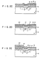
- Figs. 2A to 2E are cross sectional views of a semiconductor device, illustrating how a bipolar transistor according to this invention is manufactured.
- According to this invention, an impurity-doped poly-silicon layer is formed on a substrate. The impurity-doped poly-silicon layer will serve as a diffusion source and an interconnection electrode layer. On this poly-silicon layer an undoped poly-silicon layer is laid. The substrate with these poly-silicon layers is then subjected to thermal oxidation, whereby the impurity is diffused into the substrate and at the same time the undoped poly-silicon layer is converted to a dense silicon oxide layer with a high breakdown voltage. The substrate with the poly-silicon layer and the silicon oxide layer is thermally oxidized again at a high temperature in such a way that the impurity-doped poly-silicon layer under the silicon oxide layer has some portions changed to silicon oxide. The other portions of the impurity-doped poly-silicon layer remain unchanged, thereby providing an interconnection electrode layer having a desired pattern.
- That is, the patterning of the interconnection electrode layer is achieved by selective oxidation of the impurity-doped silicon layer, not by etching of the impurity-doped poly-silicon layer. The stepped portions of the interconnection electrode layer are therefore so low that continuous metal electrodes can be formed. Since a dense undoped silicon oxide layer of a high breakdown voltage is formed on the interconnection electrode layer, all the drawback inherent to the known methods can be removed. More precisely, a silicon nitride layer, i.e. an oxidation mask, formed on the undoped silicon oxide layer does not melt unlike in the known method because no AsSG layer is formed on the undoped silicon oxide layer which is formed on the interconnection electrode layer. For this reason the precision of patterning of the impurity-doped poly-silicon layer will not be degraded. It will not be degraded also because the silicon oxide layer formed between the silicon nitride layer and the impurity-doped poly-silicon layer is dense and thin and has a high breakdown voltage, not such a thick silicon oxide layer as is formed in the known method by CVD process.
- The undoped silicon oxide layer formed on the interconnection electrode layer has an impurity concentration of 1 x 1017 cm-3 or less. Every portion of the interconnection electrode layer has its sides put in contact with the impurity-doped silicon oxide layer which has been formed by selectively oxidizing the impurity-doped poly-silicon layer. The impurity-doped silicon oxide layer defines the interconnection electrode layer having a desired pattern, and has an impurity concentration of 1 x 1018 cm-3 to 1 x 1022 cm-3. On the impurity-doped silicon oxide layer there is formed undoped silicon oxide layer having an impurity concentration of 1 x 10" cm-3 or less. These doped silicon oxide layer and the undoped silicon oxide layer constitute a silicon oxide layer which of course consists of doped portions and undoped portions.
- According to this invention the impurity-doped poly-silicon layer may be formed by CVD method, by sputtering method or by impurity ion implantation to the undoped poly-silicon layer. Preferably the undoped poly-silicon layer is about 50-100 nm (500 to about 1,000 A). If it is more than 100 nm (1,000 A) thick, the stepped portions of the interconnection electrode layer become too high and a considerably long time is required to oxidize the impurity-doped poly-silicon layer which lies beneath the undoped poly-silicon layer.
- Proper temperature and proper time may be selected for the thermal oxidation of the impurity-doped poly-silicon layer, according to various factors such as the desired degree of impurity diffusion in the impurity-doped poly-silicon layer and the desired thickness of the undoped poly-silicon layer.
- Now referring to Figs. 2A to 2E, it will be described how a bipolar transistor was manufactured according to this invention.
- As shown in Fig. 2A, silicon oxide (Si02) was deposited by CVD method to form a
layer 13 300 nm (3,000 A) thick on the major surface of an N-type silicon substrate 12 with a P-typesilicon base region 11 formed in it. The Si02 layer 13 was selectively etched by means of photolithography, thus forming adiffusion window 14 to expose thebase region 11. Thediffusion window 14 was smaller than thebase region 11. Then, an arsenic-doped poly-silicon layer 15 200 nm (2,000 A) thick having an arsenic concentration of 1 x 1020 cm was formed by sputtering method. On the arsenic-doped poly-silicon layer 15 there was formed an undoped poly-silicon layer 16 50 nm (500 A) thick also by sputtering method. Thereafter thesubstrate 12 with thelayers silicon layer 15 into the P-type base region 11 through thediffusion window 14. As a result, anemitter region 17, i.e. an N-type diffusion region, was formed in the P-type base region 11 as illustrated in Fig. 2B. At the same time the undoped poly-silicon layer 16 was oxidized to form a dense undopedsilicon oxide layer 18. - Thereafter, as shown in Fig. 2C, a silicon nitride (Si3N4) layer 100 nm (1,000 A) thick was formed on the
silicon oxide layer 18 and selectively etched by means of photolithography, thus leaving an Si3N4 layer 19 having a desired pattern. Thesubstrate 12 with thelayers silicon oxide layer 18 lay between the arsenic-doped poly-silicon layer 15 and the S13N4 layer 19. The Si3N4 layer 19 therefore preserved its clear-cut pattern and well served as an oxidation mask. Consequently, that portion of the arsenic-doped poly-silicon layer 15 which lay beneath that portion of thesilicon oxide layer 18 on which the Si3N4 layer 19 did not exist was oxidized, whereby said portions of thelayers silicon oxide layer 20. The other portion of thelayer 15 was therefore insulated by thesilicon oxide layer 20. In this way there was provided aninterconnection electrode layer 21 which has a desired pattern and which was made of arsenic-doped poly-silicon, as shown in Fig. 2D. - The
silicon nitride layer 19 was then removed by plasma etching. This done, acontact hole 22 was formed in thesilicon oxide layer 18, thereby exposing theinterconnection electrode layer 21. Thereafter an aluminum layer was formed by vapor deposition and selectively etched in a desired pattern. As a result, as shown in Fig. 2E, there was formed analuminum electrode 23 which was connected to theemitter region 17 through theinterconnection electrode layer 21 and thecontact hole 22, whereby a bipolar transistor was manufactured. - The bipolar transistor thus manufactured had an interconnection electrode layer with a highly precise pattern and extremely low stepped portions and an aluminum electrode with no discontinuity and thus highly reliable. The silicon oxide layer lying between the interconnection electrode layer and the aluminum electrode was sufficiently dense and had no pin-holes. The bipolar transistor therefore had a sufficiently high breakdown voltage.
- In order to elevate further the breakdown voltage between the aluminum electrode and the interconnection electrode layer, a CVD-Si02, Si3N4 or SiC may be deposited before making a contact hole in the silicon oxide layer which has been converted from the undoped poly-silicon layer.
- This invention may be applied to manufacture of not only a bipolar transistor but also an MOS transistor.
- As described in detail, according to this invention, an undoped poly-silicon is deposited on an impurity-doped poly-silicon layer which serves as a diffusion source and as an interconnection electrode and is then thermally oxidized to form a dense silicon oxide layer having a high breakdown voltage. A silicon nitride layer formed on the silicon oxide layer is therefore prevented from cracking or melting, making it possible to provide an interconnection electrode having a highly precise pattern and extremely low stepped portions. A contact hole is made in the silicon oxide layer, and a metal electrode is formed which is connected to the interconnection electrode through the contact hole. The breakdown voltage between the metal electrode and the interconnection electrode is sufficiently high. It is therefore possible with this invention to manufacture a semiconductor device which has a high breakdown voltage and which is thus highly reliable.
Claims (11)
Applications Claiming Priority (2)
| Application Number | Priority Date | Filing Date | Title |
|---|---|---|---|
| JP54071042A JPS6043656B2 (en) | 1979-06-06 | 1979-06-06 | Manufacturing method of semiconductor device |
| JP71042/79 | 1979-06-06 |
Publications (3)
| Publication Number | Publication Date |
|---|---|
| EP0021133A2 EP0021133A2 (en) | 1981-01-07 |
| EP0021133A3 EP0021133A3 (en) | 1983-07-20 |
| EP0021133B1 true EP0021133B1 (en) | 1985-10-30 |
Family
ID=13449061
Family Applications (1)
| Application Number | Title | Priority Date | Filing Date |
|---|---|---|---|
| EP80103063A Expired EP0021133B1 (en) | 1979-06-06 | 1980-06-02 | Semiconductor device comprising an interconnection electrode and method of manufacturing the same |
Country Status (4)
| Country | Link |
|---|---|
| US (1) | US4403392A (en) |
| EP (1) | EP0021133B1 (en) |
| JP (1) | JPS6043656B2 (en) |
| DE (1) | DE3071207D1 (en) |
Families Citing this family (16)
| Publication number | Priority date | Publication date | Assignee | Title |
|---|---|---|---|---|
| FR2525389A1 (en) * | 1982-04-14 | 1983-10-21 | Commissariat Energie Atomique | METHOD FOR POSITIONING AN INTERCONNECTION LINE ON AN ELECTRIC CONTACT HOLE IN AN INTEGRATED CIRCUIT |
| EP0112662A1 (en) * | 1982-12-21 | 1984-07-04 | Northern Telecom Limited | Stacked MOS devices with polysilicon interconnects |
| DE3304642A1 (en) * | 1983-02-10 | 1984-08-16 | Siemens AG, 1000 Berlin und 8000 München | INTEGRATED SEMICONDUCTOR CIRCUIT WITH BIPOLAR TRANSISTOR STRUCTURES AND METHOD FOR THEIR PRODUCTION |
| JPS6063961A (en) * | 1983-08-30 | 1985-04-12 | Fujitsu Ltd | Manufacture of semiconductor device |
| JPS60138940A (en) * | 1983-12-27 | 1985-07-23 | Toshiba Corp | Manufacture of semiconductor device |
| US4555842A (en) * | 1984-03-19 | 1985-12-03 | At&T Bell Laboratories | Method of fabricating VLSI CMOS devices having complementary threshold voltages |
| EP0160941A3 (en) * | 1984-05-07 | 1987-03-25 | General Electric Company | High voltage interconnect system for a semiconductor integrated circuit |
| JPS6181653A (en) * | 1984-09-28 | 1986-04-25 | Nec Corp | Self matching dielectric isolation method of semiconductor device |
| US5084413A (en) * | 1986-04-15 | 1992-01-28 | Matsushita Electric Industrial Co., Ltd. | Method for filling contact hole |
| GB2193034B (en) * | 1986-07-25 | 1990-01-04 | Plessey Co Plc | Process for the production of bipolar devices |
| JPH02105464A (en) * | 1988-10-13 | 1990-04-18 | Nec Corp | Manufacturing method of semiconductor device |
| JP2904533B2 (en) * | 1989-03-09 | 1999-06-14 | 株式会社東芝 | Method for manufacturing semiconductor device |
| US4927773A (en) * | 1989-06-05 | 1990-05-22 | Santa Barbara Research Center | Method of minimizing implant-related damage to a group II-VI semiconductor material |
| KR920004366B1 (en) * | 1989-09-08 | 1992-06-04 | 현대전자산업 주식회사 | Method of fabricating self-aligned contact for semiconductor device |
| US5057439A (en) * | 1990-02-12 | 1991-10-15 | Electric Power Research Institute | Method of fabricating polysilicon emitters for solar cells |
| DE69123175T2 (en) | 1990-05-31 | 1997-04-03 | Canon Kk | Method of wiring a semiconductor circuit |
Family Cites Families (8)
| Publication number | Priority date | Publication date | Assignee | Title |
|---|---|---|---|---|
| US3928095A (en) * | 1972-11-08 | 1975-12-23 | Suwa Seikosha Kk | Semiconductor device and process for manufacturing same |
| US3904450A (en) * | 1974-04-26 | 1975-09-09 | Bell Telephone Labor Inc | Method of fabricating injection logic integrated circuits using oxide isolation |
| US4074304A (en) * | 1974-10-04 | 1978-02-14 | Nippon Electric Company, Ltd. | Semiconductor device having a miniature junction area and process for fabricating same |
| JPS51127682A (en) * | 1975-04-30 | 1976-11-06 | Fujitsu Ltd | Manufacturing process of semiconductor device |
| JPS5816337B2 (en) * | 1975-06-13 | 1983-03-30 | 日本電気株式会社 | Manufacturing method of semiconductor device |
| FR2340619A1 (en) * | 1976-02-04 | 1977-09-02 | Radiotechnique Compelec | IMPROVEMENT IN THE MANUFACTURING PROCESS OF SEMICONDUCTOR DEVICES AND DEVICES THUS OBTAINED |
| JPS606108B2 (en) * | 1976-07-07 | 1985-02-15 | 株式会社東芝 | Manufacturing method of semiconductor device |
| US4123300A (en) * | 1977-05-02 | 1978-10-31 | International Business Machines Corporation | Integrated circuit process utilizing lift-off techniques |
-
1979
- 1979-06-06 JP JP54071042A patent/JPS6043656B2/en not_active Expired
-
1980
- 1980-05-22 US US06/152,305 patent/US4403392A/en not_active Expired - Lifetime
- 1980-06-02 DE DE8080103063T patent/DE3071207D1/en not_active Expired
- 1980-06-02 EP EP80103063A patent/EP0021133B1/en not_active Expired
Also Published As
| Publication number | Publication date |
|---|---|
| JPS6043656B2 (en) | 1985-09-30 |
| EP0021133A2 (en) | 1981-01-07 |
| DE3071207D1 (en) | 1985-12-05 |
| JPS55163837A (en) | 1980-12-20 |
| EP0021133A3 (en) | 1983-07-20 |
| US4403392A (en) | 1983-09-13 |
Similar Documents
| Publication | Publication Date | Title |
|---|---|---|
| US4486942A (en) | Method of manufacturing semiconductor integrated circuit BI-MOS device | |
| US4609568A (en) | Self-aligned metal silicide process for integrated circuits having self-aligned polycrystalline silicon electrodes | |
| KR100227766B1 (en) | Semiconductor device and the manufacturing method thereof | |
| US4403392A (en) | Method of manufacturing a semiconductor device | |
| US4871685A (en) | Method of manufacturing bipolar transistor with self-aligned external base and emitter regions | |
| EP0091984B1 (en) | Integrated circuit devices comprising dielectric isolation regions and methods for making such devices | |
| US4641170A (en) | Self-aligned lateral bipolar transistors | |
| EP0055521B1 (en) | Method of filling a groove in a semiconductor substrate | |
| JPS62588B2 (en) | ||
| US4412378A (en) | Method for manufacturing semiconductor device utilizing selective masking, etching and oxidation | |
| CA1050667A (en) | Method of manufacturing semiconductor devices | |
| US4532696A (en) | Method of manufacturing a semiconductor device for forming a deep field region in a semiconductor substrate | |
| US3986896A (en) | Method of manufacturing semiconductor devices | |
| US4663827A (en) | Method of manufacturing a field effect transistor | |
| KR100281887B1 (en) | Manufacturing Method of Semiconductor Device | |
| KR100372675B1 (en) | Manufacturing method of semiconductor device with self-aligned silicide region | |
| US3899373A (en) | Method for forming a field effect device | |
| US4551906A (en) | Method for making self-aligned lateral bipolar transistors | |
| US4261765A (en) | Method of manufacturing a semiconductor device | |
| US4085499A (en) | Method of making a MOS-type semiconductor device | |
| US4451844A (en) | Polysilicon emitter and base contacts separated by lightly doped poly separator | |
| KR880000975B1 (en) | Semiconductor substrate and its making process | |
| US6153919A (en) | Bipolar transistor with polysilicon dummy emitter | |
| JPS6133253B2 (en) | ||
| US4410375A (en) | Method for fabricating a semiconductor device |
Legal Events
| Date | Code | Title | Description |
|---|---|---|---|
| PUAI | Public reference made under article 153(3) epc to a published international application that has entered the european phase |
Free format text: ORIGINAL CODE: 0009012 |
|
| 17P | Request for examination filed |
Effective date: 19800602 |
|
| AK | Designated contracting states |
Designated state(s): DE FR GB NL |
|
| PUAL | Search report despatched |
Free format text: ORIGINAL CODE: 0009013 |
|
| AK | Designated contracting states |
Designated state(s): DE FR GB NL |
|
| RAP1 | Party data changed (applicant data changed or rights of an application transferred) |
Owner name: KABUSHIKI KAISHA TOSHIBA |
|
| GRAA | (expected) grant |
Free format text: ORIGINAL CODE: 0009210 |
|
| AK | Designated contracting states |
Designated state(s): DE FR GB NL |
|
| REF | Corresponds to: |
Ref document number: 3071207 Country of ref document: DE Date of ref document: 19851205 |
|
| ET | Fr: translation filed | ||
| PLBE | No opposition filed within time limit |
Free format text: ORIGINAL CODE: 0009261 |
|
| STAA | Information on the status of an ep patent application or granted ep patent |
Free format text: STATUS: NO OPPOSITION FILED WITHIN TIME LIMIT |
|
| 26N | No opposition filed | ||
| PGFP | Annual fee paid to national office [announced via postgrant information from national office to epo] |
Ref country code: GB Payment date: 19950522 Year of fee payment: 16 |
|
| PGFP | Annual fee paid to national office [announced via postgrant information from national office to epo] |
Ref country code: DE Payment date: 19950607 Year of fee payment: 16 |
|
| PGFP | Annual fee paid to national office [announced via postgrant information from national office to epo] |
Ref country code: FR Payment date: 19950609 Year of fee payment: 16 |
|
| PGFP | Annual fee paid to national office [announced via postgrant information from national office to epo] |
Ref country code: NL Payment date: 19950628 Year of fee payment: 16 |
|
| PG25 | Lapsed in a contracting state [announced via postgrant information from national office to epo] |
Ref country code: GB Effective date: 19960602 |
|
| PG25 | Lapsed in a contracting state [announced via postgrant information from national office to epo] |
Ref country code: NL Effective date: 19970101 |
|
| GBPC | Gb: european patent ceased through non-payment of renewal fee |
Effective date: 19960602 |
|
| PG25 | Lapsed in a contracting state [announced via postgrant information from national office to epo] |
Ref country code: FR Effective date: 19970228 |
|
| PG25 | Lapsed in a contracting state [announced via postgrant information from national office to epo] |
Ref country code: DE Effective date: 19970301 |
|
| NLV4 | Nl: lapsed or anulled due to non-payment of the annual fee |
Effective date: 19970101 |
|
| REG | Reference to a national code |
Ref country code: FR Ref legal event code: ST |