EP0015924B1 - Circuit breaker having an electronic fault sensing and trip initiating unit - Google Patents
Circuit breaker having an electronic fault sensing and trip initiating unit Download PDFInfo
- Publication number
- EP0015924B1 EP0015924B1 EP79900294A EP79900294A EP0015924B1 EP 0015924 B1 EP0015924 B1 EP 0015924B1 EP 79900294 A EP79900294 A EP 79900294A EP 79900294 A EP79900294 A EP 79900294A EP 0015924 B1 EP0015924 B1 EP 0015924B1
- Authority
- EP
- European Patent Office
- Prior art keywords
- circuit
- trip
- pick
- resistors
- voltage
- Prior art date
- Legal status (The legal status is an assumption and is not a legal conclusion. Google has not performed a legal analysis and makes no representation as to the accuracy of the status listed.)
- Expired
Links
- 230000000977 initiatory effect Effects 0.000 title abstract description 43
- 230000007246 mechanism Effects 0.000 claims abstract description 47
- 230000001681 protective effect Effects 0.000 claims abstract description 24
- 239000004020 conductor Substances 0.000 claims description 85
- 230000004044 response Effects 0.000 claims description 14
- 239000004065 semiconductor Substances 0.000 claims description 9
- 238000003780 insertion Methods 0.000 claims description 2
- 230000037431 insertion Effects 0.000 claims description 2
- 239000003990 capacitor Substances 0.000 description 102
- 238000012360 testing method Methods 0.000 description 91
- 238000004804 winding Methods 0.000 description 31
- 230000004907 flux Effects 0.000 description 22
- 230000008859 change Effects 0.000 description 16
- 230000007935 neutral effect Effects 0.000 description 7
- XEEYBQQBJWHFJM-UHFFFAOYSA-N Iron Chemical compound [Fe] XEEYBQQBJWHFJM-UHFFFAOYSA-N 0.000 description 6
- 229920006395 saturated elastomer Polymers 0.000 description 5
- 230000001419 dependent effect Effects 0.000 description 4
- 230000001960 triggered effect Effects 0.000 description 4
- 230000006835 compression Effects 0.000 description 3
- 238000007906 compression Methods 0.000 description 3
- 230000001276 controlling effect Effects 0.000 description 3
- 238000007599 discharging Methods 0.000 description 3
- 229910052742 iron Inorganic materials 0.000 description 3
- 238000012544 monitoring process Methods 0.000 description 3
- 230000010355 oscillation Effects 0.000 description 3
- 230000000717 retained effect Effects 0.000 description 3
- 230000007704 transition Effects 0.000 description 3
- 238000013459 approach Methods 0.000 description 2
- 230000015556 catabolic process Effects 0.000 description 2
- 230000002829 reductive effect Effects 0.000 description 2
- 230000001105 regulatory effect Effects 0.000 description 2
- 230000002441 reversible effect Effects 0.000 description 2
- CWYNVVGOOAEACU-UHFFFAOYSA-N Fe2+ Chemical compound [Fe+2] CWYNVVGOOAEACU-UHFFFAOYSA-N 0.000 description 1
- XUIMIQQOPSSXEZ-UHFFFAOYSA-N Silicon Chemical compound [Si] XUIMIQQOPSSXEZ-UHFFFAOYSA-N 0.000 description 1
- 230000004913 activation Effects 0.000 description 1
- 238000001816 cooling Methods 0.000 description 1
- 230000007423 decrease Effects 0.000 description 1
- 230000005611 electricity Effects 0.000 description 1
- 239000012634 fragment Substances 0.000 description 1
- 238000009434 installation Methods 0.000 description 1
- 239000000463 material Substances 0.000 description 1
- 230000005405 multipole Effects 0.000 description 1
- 230000036961 partial effect Effects 0.000 description 1
- 229910052710 silicon Inorganic materials 0.000 description 1
- 239000010703 silicon Substances 0.000 description 1
- 239000007787 solid Substances 0.000 description 1
- 230000000007 visual effect Effects 0.000 description 1
- 230000003313 weakening effect Effects 0.000 description 1
Images






Classifications
-
- H—ELECTRICITY
- H01—ELECTRIC ELEMENTS
- H01H—ELECTRIC SWITCHES; RELAYS; SELECTORS; EMERGENCY PROTECTIVE DEVICES
- H01H71/00—Details of the protective switches or relays covered by groups H01H73/00 - H01H83/00
- H01H71/10—Operating or release mechanisms
- H01H71/12—Automatic release mechanisms with or without manual release
- H01H71/14—Electrothermal mechanisms
- H01H71/16—Electrothermal mechanisms with bimetal element
-
- H—ELECTRICITY
- H02—GENERATION; CONVERSION OR DISTRIBUTION OF ELECTRIC POWER
- H02H—EMERGENCY PROTECTIVE CIRCUIT ARRANGEMENTS
- H02H3/00—Emergency protective circuit arrangements for automatic disconnection directly responsive to an undesired change from normal electric working condition with or without subsequent reconnection ; integrated protection
- H02H3/08—Emergency protective circuit arrangements for automatic disconnection directly responsive to an undesired change from normal electric working condition with or without subsequent reconnection ; integrated protection responsive to excess current
- H02H3/093—Emergency protective circuit arrangements for automatic disconnection directly responsive to an undesired change from normal electric working condition with or without subsequent reconnection ; integrated protection responsive to excess current with timing means
-
- H—ELECTRICITY
- H02—GENERATION; CONVERSION OR DISTRIBUTION OF ELECTRIC POWER
- H02H—EMERGENCY PROTECTIVE CIRCUIT ARRANGEMENTS
- H02H3/00—Emergency protective circuit arrangements for automatic disconnection directly responsive to an undesired change from normal electric working condition with or without subsequent reconnection ; integrated protection
- H02H3/08—Emergency protective circuit arrangements for automatic disconnection directly responsive to an undesired change from normal electric working condition with or without subsequent reconnection ; integrated protection responsive to excess current
- H02H3/10—Emergency protective circuit arrangements for automatic disconnection directly responsive to an undesired change from normal electric working condition with or without subsequent reconnection ; integrated protection responsive to excess current additionally responsive to some other abnormal electrical conditions
- H02H3/105—Emergency protective circuit arrangements for automatic disconnection directly responsive to an undesired change from normal electric working condition with or without subsequent reconnection ; integrated protection responsive to excess current additionally responsive to some other abnormal electrical conditions responsive to excess current and fault current to earth
Definitions
- This invention relates to the field circuit breakers for protection of electrical circuits, and in particular to those having adjustment means to vary certain performance characteristics of the breaker, such as its ampere rating, trip times and the like.
- Circuit breakers having been in use for many years to protect electrical circuits in homes as well as in commercial and industrial establishments, and wherever electricity is used.
- the typical circuit breaker includes a mechanical tripping mechanism and magnetic or thermal triggering means to open the circuit on occurrence of an overcurrent fault of a pre-selected magnitude.
- the tripping level of such circuit breakers is usually set by the manufacturer and either cannot be changed by the user or if adjustment of the trip level is provided it can only be done within a relatively limited range and without knowing precisely what the change is.
- Resistor circuits provide control and output signal for said pick-up circuits, and each pick-up circuit has a respective output circuit which is controlled by the respective pick-up circuit to provide a respective output pulse to gate the SCR which triggers the coil.
- One output circuit includes a means for controlling the timing of its output thus providing for the lapse of predetermined time from the application of the respective first D.C. signal to a pick-up circuit.
- a resistor circuit is included serially connected between said reference signal means and the respective output circuit of another pick-up circuit to control the respective output circuit for gating said semiconductor device in a time period less than said predetermined time in response to the application of a respective first D.C. signal to the other pick-up circuit.
- another resistor circuit controls the time duration in which the respective output circuit for the ground fault pick-up circuit gates the SCR.
- switches are included for the resistor circuits.
- the operating mechanism 4 is mounted in the circuit breaker case 6, comprising a base portion 6a and a cover portion 6b.
- the operating mechanism 4 includes an operating assembly 7 connected to move the movable contacts 8 of each pole between a contact open position and contact closed position with reference to the respective stationary contacts 9 of each pole.
- Movable contacts 8 are conductively connected respectively to corresponding terminals 10 of each pole at end 11 of the circuit breaker 1.
- Stationary contacts 9 are conductively connected respectively to corresponding terminals 11 of each pole at the opposite end 12 of the circuit breaker 1.
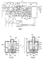
- the electronic fault sensing and trip initiating unit 2 includes three current transformers 15, 16 and 17, comprising cores 18,19 and 20 and in which internal bus bars 21, 22 and 23 of the breaker leading from _terminals 10a, 10b and 10c are the respective primaries.
- a secondary winding 24 is provided for current transformer 15, secondary winding 25 for current transformer 16 and secondary winding 26 for current transformer 17.
- a differential transformer 27 is mounted on a frame 28 secured to a support member 28a of the circuit breaker 1 over the center pole of the breaker adjacent the end 11.
- Differential transformer 27 includes a summing toroid 29, primary windings 30, 31 and 32 connected at first terminals thereof in series respectively with first terminals of secondary windings 24, 25 and 26 of respective current transformers 15, 16 and 17, by respective conductors 33, 34 and 35.
- the respective second terminals of primary windings 30, 31 and 32 are connected in series with first terminals of respective primary windings 36, 37 and 38 of step-up transformers 39, 40 and 41 by respective conductors 42, 43 and 44.
- the respective second terminals of primary windings 36, 37 and 38 are connected to respective second terminals of the secondary windings 24, 25 and 26 of current transformers 15, 16 and 17, by respective conductors 45, 46 and 47.
- the current transformers 15, 16 and 17 thus feed step-up transformers 39, 40 and 41 described more fully herein below.
- the current transformers also feed the primary windings 30, 31 and 32 of the differential transformer 27. Since current transformers 15, 16 and 17 are fed by the bus bar of each pole of the circuit breaker 1, in a three-wire grounded neutral A.C. distribution circuit one of them is inductively connected to the neutral conductor and the other two to the line conductors of the circuit.
- the primary of differential transformer 27 connected in series with the secondary of the neutral connected current transformer likewise carries the current induced from the neutral conductor while the other two carry the current induced from the two line conductors in such three-wire circuit.
- the differential transformer 27 also includes a secondary winding 48, connected by conductors 49 and 50 to an electronic ground fault interrupting circuit as more fully described hereinbelow. While the sum of the currents and magnetic flux in the primaries 30, 31 and 32 are zero, there is no pick-up or voltage induced in secondary winding 48. However, if one of the line conductors becomes grounded on the load side, a portion of the current returns to source through a ground path rather than through the neutral conductor to which one of the current transformers 15, 16 or 17 and one of the primaries 30, 31 or 32 of the differential transformer 27 are inductively coupled.
- differential transformer 27 which is coupled to the neutral conductor carries less current than the sum of the currents flowing in the line conductors, an imbalance of magnetic flux occurs which then induces a voltage signal in secondary winding 48.
- signal is transmitted by conductors 49 and 50 to means connected to the ground fault interrupting circuit, and if of sufficient magnitude it will trip the circuit breaker 1 and interrupt the circuit.
- a fourth primary winding 51 is provided on the summing toroid 29 of differential transformer 27 for use in four wire circuits.
- This fourth primary winding 51 is connected at a first terminal to conductor 52 which leads to a first terminal screw 53 of a terminal block 54, and is connected at a second terminal to conductor 55 which leads to a second terminal screw 56 on terminal block 54.
- the terminal block 54 is mounted on the cover portion 6b of circuit breaker case 6, for convenient access from outside of the breaker.
- a separate current transformer 57 is mounted at any convenient location in the vicinity of the circuit breaker 1, the fourth bus bar or other conductor of the fourth wire system is series connected through the core 58 of the separate current transformer 57, such series connection through the core becoming the primary winding of such current transformer.
- a secondary winding 59 is provided on the core 58 of transformer 57, and the first and second terminals of such secondary 59 may then be connected respectively to first and second terminal screws 53 and 56 on terminal block 54.
- the step-up transformers 39, 40 and 41 include secondary windings 60, 61 and 62 respectively.
- the secondary windings of the step-up transformers are connected to respective terminals on an ampere rating adjustment assembly 63, by respective conductors 64 and 65 leading from the terminals of secondary winding 60, conductors 66 and 67 leading from the terminals of secondary winding 61, conductors 68 and 69 leading from the terminals of secondary winding 62.
- the conductors 49 and 50 leading from secondary winding of differential transformer 27 also lead to respective terminals on the ampere rating adjustment assembly 63.
- overcurrent faults sensed by current transformers 1 5 " 16 and 17 are fed through step-up transformers 39, 40 and 41 to the ampere rating adjustment assembly 63, and ground faults sensed by differential transformer 27 are also fed to the ampere rating adjustment assembly 63.
- the ampere rating adjustment assembly 63 includes a terminal slot 64 in the base portion 6a of the circuit breaker case 6 having conductive strips connected to the respective terminals to which conductors 64, 65, 66, 67, 68 and 69 (from the step-up transformers) as well as conductors 49 and 50 (from the differential transformer) are connected, and an ampere rating plug 70 having a stab portion 71 with conductive strips 72 for contact with corresponding conductive strips of the terminal slot 674 when the stab 71 of ampere rating plug 70 is inserted therein.
- the ampere rating plug 70 includes four resistors 73, 74, 75 and 76 mounted therein and connected respectively to separate pairs of conductive strips 72, for connection to respective pairs of conductive strips in terminal slot 64.
- ampere rating plug 70 When ampere rating plug 70 is inserted into the terminal slot 64, respective ones of the resistors 73, 74, 75 and 76 are connected across respective conductor pairs 64---65, 66-67, 68-69 (leading from the secondaries of the step-up transformers 39, 40 and 41) and 49-50 (leading from the secondary of differential transformer 27).
- the value of the resistors 73, 74, 75 and 76 determines the ampere rating of the circuit breaker.
- the ampere rating of the breaker is therefore adjustable by providing a plurality of ampere rating plugs 70, each having mounted therein resistors of different selected values to enable varying the ampere rating of the breaker to chosen percentages of a base ampere rating.
- the circuit breaker illustrated in the drawings and used as the basis of the description herein may have a base or normal ampere rating of 2,000 amperes.
- a set of five ampere rating plugs, of which ampere rating plug 70 is an example, may be provided with resistors of different values to change the ampere rating of the breaker from 2,000 amperes to 1,000 amperes in increments of 200 amperes. That is to say, one rating plug would reduce the ampere rating 200 amperes, from 2,000 A. to 1,800 A.
- a second rating plug would contain resistors of such value that would reduce the ampere rating 400 amperes, from 2,000 A. to 1,600 A., and so on. It is of course possible and within the scope of this invention to choose different resistance values to conveniently provide different ampere ratings of a circuit breaker, other than those set forth above as example.
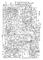
- the overcurrent fault trip initiating circuits include an input section comprising a rectified power supply, a pick-up stage, a long time delay circuit, a short time delay circuit, an instantaneous trip circuit, and an electronic switching stage to initiate tripping of the circuit breaker.
- Conductors 84 and 85 provide a ground fault signal voltage to grids 89 from differential transformer 27, in which all three phases (or four in a four wire system) of the circuit breaker serve as primary windings.
- the ground fault trip initiating circuit will be described in greater detail below.
- Resistors 96 and 97 are connected in series to conductor 94, and a four position ampere rating adjustment switch 98 is connected to conductor 94 at various settings in relation to resistors 96 and 97.
- the four position adjustment switch 98 operates by connecting the two poles adjacent whatever adjustment level the switch is set at As shown in the drawing (Figs. 4 and 5), when set at the 100% adjustment level, the two pins on each side of the designation 100% are connected which eliminates the switch entirely thus directing current through both of the associated resistors 96 and 97. When set at the 90% adjustment level, the two pins on each side of that designation are connected which shorts out resistor 96 so current is directed through resistor 97.
- Resistor 97 has a relatively higher resistance value than resistor 96, for example 4.7 Kohms for resistor 97 and 2.7 Kohms for resistor 96.
- switch 98 When switch 98 is set at the 80% adjustment level, the two pins on each side of that designation are connected which shorts out resistor 97 (having relatively higher resistance) and directs current through resistor 96 (having relatively lower resistance).
- switch 98 When switch 98 is set at the 70% adjustment level, the two pins on each side of that adjustment designation are connected which shorts out both resistors so the current completely bypasses the resistors 96 and 97.
- the higher the resistance in the output circuit from rectifiers 86, 87 and 88 the higher the ampere rating of the circuit breaker.
- a low output from the rectification bridges 86, 87 and 88 leads through conductors 94 and 95 to capacitor 90 charging it to a pre-determined voltage.
- the ampere rating adjustment switch 98 is set at the 80% rating for example, the impressed voltage on capacitor 90 is about 12 volts.
- the output signal is also directed through resistor 99 and zener diode 100 to circuit ground.
- a ground current path leads from the components which are circuit ground connected to the circuit ground connections of conductors 101, 102 and 13 leading to rectification bridges 86, 87 and 88 respectively, thus completing the electronic circuit of the DC power supply.
- the reverse breakdown voltage of zener diode 100 is at about 50% of the input. voltage.
- the voltage drop across resistor 99 results in a lowering of the voltage of the emitter of the N-P-N transistor 104 to about 7 volts (as compared to about 12 volts on capacitor 90).
- Transistor 104 is conducting during normal current no fault operating conditions with a current path through its emitter being directed through resistor 105 leading to the base of transistor 106 and resistor 107 leading to the collector of transistor 106, which is also conducting during normal current no fault conditions.
- the current path through the emitter of transistor 106 leads through resistor 108 and common conductor 109 to circuit ground through a ground terminal 110.
- the capacitor 111 which is in parallel with resistor 108 is charged to a small voltage to stabilize the circuit.
- the voltage divider network just described serves in conjunction with the ampere rating adjustment switch 98 and its associated resistors 96 and 97 to set a reference voltage above which the transistor 118 begins to conduct, and below which it remains non-conductive.
- the DC voltage from the associated rectification bridge 86, 87 or 88 through the switch/resistor combination 96, 97 and 98 through the voltage divider network rises above the reference voltage to render transistor 118 conductive and thus initiate activation of other components in the long time delay tripping circuit.
- the reference voltage is set at about 15 volts when the ampere rating adjustment switch 98 is set at 70%, at about 17 volts when set at 80%, at about 19.2 volts when set at 90%, and at about 21.3 volts when set at 100%.
- resistor 123 The current path through resistor 123 is then shunted through conductor 124 in which capacitor 125 is normally charged through resistor 123 to somewhat less than 1/2 of the voltage which appears at the first base 121 of unijunction component 122, that is during normal operating no fault conditions at which time unijunction 122 is not conducting through its second base 126.
- capacitor 125 When the full rectified output is directed to capacitor 125 through resistor 123, it charges to about 1/2 of the voltage which appears at base 121 of unijunction transistor 122 causing unijunction 122 to change state and capacitor 125 to discharge.
- the unijunction When it changes state, the unijunction begins to conduct through its second base 126, thus providing a current path from the emitter 127 of unijunction 122, through its second base 126, resistor 128, common conductor 109 and circuit ground terminal 110. This provides an input signal to the base of transistor 129 through diode 130 driving transistor 129 into saturation as described further hereinbelow. The unijunction transistor 122 then resets.
- the components consisting of resistors 108, 120, 123, 128, and 130, capacitor 125, unijunction 122 and diode 130 comprise a relaxation oscillator circuit which delivers a series of oscillations or pulses to a pulse generator circuit at a pulse rate which is essentially linearly related to the input voltage of the fault condition being sense.
- the pulse rate is slower than for a high magnitude fault and in each case the pulse rate is proportional to the magnitude of the input voltage of the fault.
- the function of the diode 130 is to isolate the relaxation oscillator state from the pulse generator stage.
- transistor 129 When transistor 129 changes to its original non-conducting state and transistor 131 to its original saturated or conducting state, the capacitor 136 then continues to charge through resistor 133 up to about the input voltage of the circuit. The cycle is prepared on receipt of the next oscillation or pulse from unijunction component 122 of the relaxation stage on the base of transistor 129.
- capacitor 136 charges from input voltage negative to input voltage positive, and the change of state of transistors 129 (from saturated to non-conducting) and 131 (from non-conducting to saturated) occurs at about half way between these extremes.
- the pulse width of the pulse generator output is therefore essentially independent of voltage, although the amplitude of the pulse output and the rate of the pulse output are linearly related to the input voltage of the fault condition being sensed.
- the output pulses from the collector of transistor 131 in the pulse generating stage are fed to an integrating stage which consists of resistors 138 through 146, capacitors 147, 148 and 149, N-P-N transistors 150, programmable unijunction transistor 151 and diodes 152, 153, 154, 155 and 156.
- Such pulses from the collector of transistor 131 are applied to the capacitor 149 through resistor 140 and potentiometer 141.
- the diode 154 between resistor 141 and capacitor 149 serves as a low leakage component to prevent leakage discharge of the capacitor during that part of the cycle when the pulse is not present.
- the charge on the capacitor 149 increases until it reaches a value which is determined by the voltage on the gate of the unijunction transistor 151.
- the voltage charge on the capacitor 149 and on the anode 157 of unijunction 151 is about 0.6 volts greater than the voltage on the gate 158 of the unijunction transistor 151
- the capacitor discharges into resistor 145 which is in turn applied through conductor 159-and diode 160 to the gate of the electronic switch, SCR (silicon controlled rectifier) 161.
- SCR 161 then turns on and energizes a tripping mechanism described in detail hereinbelow to trip'the circuit breaker.
- variable reference voltage supplied to gate 158 of unijunction transistor 151 also serves to minimize leakage from the capacitor 149 though the unijunction transistor 151. If the voltage on the anode 157 of unijunction 151 increases by more than 0.6 volts above the voltage on the gate 158, the unijunction transistor 151 changes state from very high impedance (open circuit and non-conducting) to low impedance (closed circuit and conducting). Thus, as long as the reference voltage on the gate 158 is kept at more than 0.6 volts above the voltage on the capacitor 149 and the anode 157 of unijunction transistor 151, leakage of the charge on the capacitor will be minimized.
- Such variation of the reference voltage level is accomplished as follows. When a pulse is being supplied to capacitor 149 from the collector 131 in the pulse generating stage, through resistor 140 and potentiometer 141, base drive is also being supplied to switching transistor 150 through resistor 138 driving it into saturation. A current path is then established from conductor 112, through resistor 146, resistor 144, zener diode 153, resistor 142, the collector emitter circuit of transistor 15C and circuit ground terminal 110. This current path through the voltage dividing net- work described results in establishing a voltage at junction Y at whatever pre-determined level desired for operation of the long time delay tripping circuit. Such reference voltage at junction Y is applied to the gate 158 of unijunction 151 during the time that capacitor 149 is being charged by a pulse received from the pulse generator stage.
- the unijunction transistor When the magnitude and duration of the pulses from the pulse generating stage charge the capacitor 149 to more than about 0.6 volts above the reference voltage on gate 158 of unijunction transistor 151, the unijunction transistor changes state and conducts discharging capacitor 149 through resistor 145, conductor 159, diode 160, gating SCR 161 into conduction and delivering a tripping voltage to the tripping mechanism more fully described hereinbelow to trip the breaker and interrupt the circuit.
- the long time delay tripping circuit described above produces a time delay which is inversely proportional to the square of the applied voltage.
- the gate voltage applied to unijunction transistor 151 must be a function of applied voltage.
- the reference voltage network described above provides such a variable reference voltage which varies as a function of applied voltage.
- a diode 152 and a resistor 162 are connected in series through conductor 163 with capacitor 149.
- a current path is provided by conductor 163 through which the charge on capacitor 149 can leak away at a controlled rate, the rate being pre-determined by the values selected for the diode 152 and resistor 162.
- the pre-determined leakage rate is chosen to correspond to the cooling rate of physical components of the circuit breaker and its associated electrical distribution system.
- the reference voltage on gate 158 is maintained at such level of 0.6 volts or more above the voltage on capacitor 149 when the input voltage of the long time delay circuit drops below the retained voltage on capacitor 149 by capacitor 147 in conjunction with resistor 143 and diode 155.
- Capacitor 147 is charged through resistor 143 when the integrating stage is receiving an output from the pulse generating stage.
- the resistor 144 limits the rate of charging of capacitor 147 such that it does not interfere with the function of the reference voltage network described above.
- the change on capacitor 147 is held by diode 155, which is series connected with capacitor 147 and positioned to block discharge thereof.
- Capacitor 147 is series connected to junction Y (connected to the terminal of gate 158 of unijunction 151), and diode 155 is cathode connected in series with junction Y.
- junction Y connected to the terminal of gate 158 of unijunction 151
- diode 155 is cathode connected in series with junction Y.
- a short time delay trip initiating circuit is provided to sense overcurrent faults of high magnitude and initiate tripping of the breaker with less time delay than that provided by the long time delay circuit described above.
- the short time delay circuit includes a pick-up stage and a voltage dependent time delay stage. Both the pick-up stage and time delay stage are adjustable by means of a resistor network and switch.
- the pick-up circuit includes resistors 164, 165,166,167,168,169,170,171,172,173, 174, 175 and, transistors 178 and 179, diodes 180 and 181, capacitors 182, 183 and 184.
- transistor 179 At voltage levels below the pre-determined pick-up voltage of the short time delay circuit, transistor 179 is conducting through resistor 172 series connected to its collector and through resistor 173 leading to ground terminal 185 connected in series to its emitter. The transistor 179 receives base drive through resistor 171 and variable resistor or potentiometer 170. The capacitor 183 which is connected across the emitter and collector circuit of transistor 179 is not able to charge above the 1.0 volt while this transistor is conducting. There is therefore no output from the pick-up stage of such voltage levels.
- base drive to transistor 178 reaches the level which causes it to change state and begin to conduct through it collector emitter circuit. This results in a low voltage at junction Z, the base terminal connection of transistor 179, causing it to change state and become non-conducting.
- the collector voltage of transistor 179 then rises to approximately the regulated voltage level which will cause the relaxation oscillator stage of the short time delay circuit to begin operating, as provided between the resistor 172 and capacitor 183 to prevent charging the capacitor through this resistor 172.
- the capacitor 183 is charged from the input voltage through a resistance network in the relaxation oscillator stage as also explained more fully below.
- the relaxation oscillator stage consists of resistors 187, 188, 174, 176 and 177, capacitors 183 and 9, and programmable unijunction 189.
- the capacitor 183 is charged from the input voltage which appears on conductor-112 leading from the ampere rating adjustment switch 98 (described above), through resistors 133 and 174 and then through the short time delay pick-up adjustment switch assembly 190 comprising a resistance network which sets both the pick-up level of the short time delay circuit and the time delay for each pick-up level.
- Switch 190 is four position slide switch which includes two sets of five pins each, the first set 191 controlling the pick-up level and the second set 192 controlling the maximum time delay setting for each pick-up level.
- the switch operator is movable to four positions, and in each position it connects the two adjacent pins of the first set 191 and the two adjacent pins of the second set 192.
- the pick-up levels may be set for an overcurrent fault of 200% at the setting designated 2X or 200%; 400% at the setting designated 4X or 400%; 500% at the setting designated 5X or 500%; and 600% overcurrent at the setting designated 6X or 600%.
- resistor 166 is shorted out, leaving resistors 165 and 167 in the circuit controlled by the first pin set 191; and resistor 187 shorted out, leaving resistor 188 in the circuit controlled by the second pin set 192.
- resistors 165, 166 and 167 are in the circuit controlled by the first pin set 191; and both resistors 187 and 188 are in the circuit controlled by the second pin set 192.
- the resistors controlled by the first pin set 191 may have the following relative values:
- the resistors controlled by the second pin set may have the following relative values:
- the relaxation oscillator stage begins to operate when the voltage charge on capacitor 183 (received from input conductor 112 through resistors 133 and 174 and through the second pin set 192 of adjustment switch 190) builds up to 0.6 volts above the reference voltage supplied to the gate 195 of unijunction transistor 189.
- the voltage on capacitor 183 reaches 0.6 volts thus making the anode 196 of unijunction 189 0.6 volts positive relative to its gate 195, the unijunction transistor 189 changes state and becomes conductive.
- Capacitor 183 then discharges through resistor 177, through diode 197, gating SCR 161 into conduction causing the breaker to trip.
- An instantaneous trip initiating circuit is provided for very high overcurrent faults, consisting of a resistor in series with a zener diode 199 and a trigger diode 200, connected to the input DC supply by conductor 112.
- a resistor in series with a zener diode 199 and a trigger diode 200
- the input DC supply by conductor 112. When the input on conductor 112 reaches about 125 volts, the reverse breakdown point of zener diode 199 is reached allowing current to pass to trigger diode 200 which in turn passes current through conductor 201 to trigger SCR 161 in conduction to trip the circuit breaker without any time delay.
- a ground fault trip initiating circuit is also provided for protection of the breaker and distribution system against ground faults of a magnitude which would not be sensed and picked up by the other trip initiating circuits.
- the ground fault trip circuit includes a pick-up stage and a time delay stage.
- a ground fault would be sensed by differential transformer 27 when one of the phases of the distribution circuit becomes grounded on the load side of the breaker, whereupon a portion of the current would return to the source through a ground path rather than through the neutral conductor of the system.
- the currents, and magnetic flux, at differential transformer 27 would thus be imbalanced, resulting in net magnetic flux to be picked up in the secondary winding 48.
- the rectified ground fault output from bridge 89 is carried to storage capacitor 90 through resistor 203, diode 204, the pick-up adjustment switch 98, and conductors 94 and 95.
- Capacitor 90 leads to circuit ground, and ground terminal connection 205 of bridge 89 completes the ground circuit.
- the resistor 203 in combination with zener diode 206 limits the voltage from the ground fault which is applied to storage capacitor 90 and to the ground fault pick-up and delay circuits. This is done to prevent the short time delay trip initiating circuit from responding to the voltage that would appear on storage capacitor 90 if the voltage were not limited, and to allow a substantially constant charging voltage to be applied to the time delay capacitor 207.
- the pick up stage of the ground fault trip initiating circuit includes transistors 208 and 209, resistors 203, 210 through 222, capacitors 223 and 207.
- Resistor 215 is a variable resistor.
- the pick-up voltage level on the ground fault trip initiating circuit is determined by the voltage dividing network consisting .of resistor 214, variable resistor 215, resistors 216 and 217, and such voltage is applied to the gate 224 of the unijunction transistor 225 through conductor 226 and resistor 221.
- the pick-up voltage level on the ground fault trip initiating circuit is adjustable internally at the factory by changing the setting of variable resistor 215, but it is not externally adjustable by the user.
- transistor 209 is conducting and transistor 208 is non-conducing.
- transistor 209 is conducting, a current path extends from the DC power supply input through conductors 94 and 95, transistor 104, conductors 227 and 228, through resistor 218 to the base of transistor 208, through resistor 219 to the collector of transistor 209, through resistor 220 and then to circuit ground terminal 229.
- Transistor 208 is non-conducting at conditions below the pick-up voltage level of the ground fault trip initiating circuit.
- transistor 209 While transistor 209 is conducting, a low voltage of about 1.0 to 1.5 Volts is present at its collector and at the junction XX between the collector of transistor 209 and the cathode of the diode 230 which is anode connected to the time delay capacitor 207. Thus, while such low voltage is present at junction XX, capacitor 207 cannot be charged to more than approximately 1.0 to 1.5 volts since current flowing through the resistor network 210, 211, 212 and 213 to the junction between capacitor 207 and the anode side of diode 230 will find a low voltage path through diode 230 to junction XX.
- the switch circuit includes resistor 211, 212 and 213, which can be shorted out and inserted into the capacitor charging circuit in various combinations depending on the switch setting.
- the resistors have varying relative values; for example, resistor 211 may be 680 Kohms, resistor 212 may be 1.5 Megohms, and resistor 213 may be 620 Kohms.
- pins 231 a and 231 b are connected, which shorts out resistors 211, 212 and 213 leaving no resistance in the switch circuit itself or a time delay of 100 milliseconds in the example given.
- pins 231 b and 231 c are connected, which shorts out resistors 212 and 213 leaving resistor 211 in the switch circuit to provide a switch circuit resistance of 680 Kohms in the example given for a time delay of 200 milliseconds.
- pins 231c and 231d When set at the .3 position pins 231c and 231d are connected, which shorts out resistor 212 leaving resistors 211 and 213 in the switch circuit to provide switch circuit resistance of 680 Kohms plus 620 Kohms for a total of 1.3 Megohms which provides a time delay of 300 milliseconds in the example given.
- pins 231d and 231e When set at the .5 position, pins 231d and 231e are connected, which inserts all three resistors 211, 212 and 213 in the circuit to provide switch circuit resistance of 2.8 Megohms for a time delay of 500 milliseconds in the illustrative circuit shown and described herein.
- Capacitor 207 is connected to the anode 232 of unijunction transistor 225.
- the unijunction transistor changes state from very high impedance (resembling an open circuit) to low impedance.
- Capacitor 207 then discharges into resistor 233 and 234 to gate an electronic switch comprising an SCR 235 into conduction, and also discharges into resistor 236 to gate SCR 161 into conduction which initiates tripping of the breaker.
- the SCR 235 is connected to a solenoid described later herein which actuates visual indication means to indicate that the breaker tripped due to a ground fault condition.
- Internal ground fault trip indication terminals 237 and 238 are connected to terminals 237a and 238a on terminal block 54.
- a separate electronic monitoring assembly having an indicator lamp, of the type described in Patent No. 3,943,409 assigned to the assignee of the present application, can be connected to terminals 237a and 238a for external or remote indication of tripping due to a ground fault condition.
- the ground fault indicator solenoid is energized by the discharge of capacitor 239 through terminal 238 switched by SCR 235.
- the capacitor 239 is charged from the ground fault differential transformer 27 through bridge 89 and resistor 203 upon occurrence of a ground fault.
- electronic switch SCR 161 is triggered by a pulse from the discharge of capacitor 207. This same pulse also triggers SCR 235 into conduction and allows capacitor 239 to discharge through the ground fault trip indicator solenoid SCR 235, and circuit ground terminal 240.
- the externally mounted electronic monitoring assembly having an indicator lamp to indicate a trip due to a ground fault condition requires a pulse of a certain magnitude and duration, such as 32 volts with a duration of at least one millisecond. This is provided by combining the signal appearing on internal terminal 238 with a pulse which appears on internal terminal 237.
- the pulse at terminal 237 is provided by the circuit consisting of resistors 241 and 242, capacitor 243 and diode 244.
- the capacitor 243 is charged through about 24 volts for example upon the occurrence of a ground fault, the charging voltage selected depending on the relative values of the other components in the circuit.
- the ground fault trip occurs and SCR 235 is triggered into conduction forcing the positive side of capacitor 243 to ground. Since the capacitor discharge path is blocked by diode 244, the output to terminal 237 will be approximately -24 volts in the example given for purposes of illustration.
- the voltage on terminal 238 charged by capacitor 239 in the embodiment described herein is +24 volts, so the potential difference between terminals 237 and 238 is +48 volts, which is the output available for the externally mounted electronic monitoring assembly having a ground fault trip indicating lamp.
- the electronic switch 161 is triggered into conduction by voltage signals transmitted from either the long time delay trip circuit, the short time delay trip circuit, the instantaneous trip circuit or the ground fault trip circuit to the gate 245 of SCR 161.
- a capacitor 246 and resistor 247 are provided in parallel with the cathode - gate circuit of SCR 161 for the purpose of suppressing transients and noise which might otherwise trigger the SCR 161 into conduction.
- the tripping energy is supplied to the tripping coil controlled by SCR 161 by storage capacitor 90 discharging through conductor 94, energizing the tripping coil and through SCR 161 to circuit ground through circuit ground terminal 248.
- the circuit breaker includes means for a user to test the various trip initiating circuits when desired to determine that the circuits are in proper operating condition.
- Such means includes test terminals 251 through 258.
- One series of tests will enable the user to conveniently test the pick-up levels of the long time delay trip initiating circuit, the short time delay trip initiating circuit and the ground fault trip initiating circuit.
- a second series of tests will enable the user to conveniently test the pick-up levels of the long time delay trip initiating circuit, the short time delay trip initiating circuit and the ground fault trip initiating circuit.
- a second series of tests will enable the user to conveniently test the time delay section of the circuitry.
- An appropriate testing device may be connected to a conventional 120 AC power supply, and will provide a DC output of from 0 to 150 volts. It includes a terminal insert corresponding to the ampere rating adjustment plug 70, which is inserted into the terminal slot 64 in the base of the circuit breaker being tested. The ampere rating adjustment plug 70 is removed from the breaker and inserted into a corresponding terminal slot in the testing device, so the same ampere rating of the breaker is applied to the testing device.
- the testing device includes a pair of output conductors having connecting terminals for connecting to corresponding terminals at appropriate test points in the electronic circuits to be tested for the purpose of applying an appropriate test voltage to the circuits being tested.
- test portion of the circuitry which is included as part of the invention covered by the present application is that which is physically incorporated in the circuitry of the circuit breaker itself.
- the short time delay trip initiating circuit includes a test point terminal 251 connected between the collector of transistor 179, resistor 172 and diode 181.
- the long time delay trip initiating circuit includes a test point terminal 252 connected between the collector of transistor 106, resistor 107 and diode 164.
- the ground fault trip initiating circuit includes a test point terminal 253 connected between the collector of transistor 209, resistor 219 and diode 230.
- a voltage input test terminal 254 is connected to storage capacitor 90 to provide test voltages to the short time delay and long time delay circuits respectively as they are being tested.
- a short-to-ground test terminal 256 is provided, connected between the gate 245 of electronic switch SCR 161 and the output conductors of the various trip initiating circuits, to short the electronic switch out to ground and prevent actual tripping of the circuit breaker during the short time delay test.
- the time between sensing such faults and tripping is so short (e.g. less than one second), so it is desirable for measuring response during a test of the short time delay circuit to avoid actual tripping of the breaker.
- a circuit ground test terminal 257 is provided for connecting to ground terminal 248 of the circuit.
- a ground terminal lead from the testing device is connected to test terminal 257 to complete the circuit which begins at input test terminal 254 which receives an input test voltage through a lead from the testing device, or at a second input test terminal 258 described in the next paragraph.
- a second voltage input test terminal 258 is provided to supply an appropriate test Voltage to the ground fault trip initiating circuit.
- Test terminal 258 is connected to the ground fault trip initiating circuit between resistor 203, diode 204, and the ground fault indicator solenoid.
- Test terminal 258 is also connected to terminal 238 which receives the discharge from capacitor 239 as it is applied to the ground fault indicator solenoid on occurrence of a ground fault of tripping magnitude and duration.
- the testing device supplies the simulated ground fault voltage to terminal 258 which the rectification bridge 89 normally supplies to terminal 238 on occurrence of an actual ground fault condition in the distribution circuit protected by the circuit breaker of this invention.
- the testing means in accordance with this invention operates as follows. After connecting the terminal insert of the testing device in terminal slot 64 of the circuit breaker, and the ampere rating adjustment plug 70 in a corresponding terminal slot of the testing device, the voltage output lead of the testing device is connected to terminal 254 of the circuit breaker and the ground terminal lead of the testing device is connected to terminal 257 of the circuit breaker.
- test terminal 251 in the short time delay circuit and test terminal 253 in the ground fault circuit could be shorted out by connection thereto of the short-out leads.
- test terminal 251 in the short time delay circuit and test terminal 252 in the long time delay circuit are shorted out by connecting the short-out leads to such terminais.
- the first test may be of the pick-up stage of the long time delay circuit.
- a simulated overcurrent voltage of about 15 volts or above is applied to test terminal 254, whereupon a transition from low voltage (e.g. 1.5 volts) to high voltage (e.g. 7 volts) should appear at test terminal 252 if the pick-up stage of the long time delay circuit is operating properly.
- the next test may be of the pick-up stage of the time delay circuit.
- a simulated overcurrent voltage of about 26 volts or above is applied to test terminal 254, whereupon a transition from low voltage (e.g. 1.5 volts) to high voltage (e.g. 7 volts) should appear at test terminal 251 if the pick-up stage of the short time delay circuit is operating properly.
- a third test may be of the pick-up stage of the ground fault time delay circuit.
- a simulated ground fault voltage of about 18 volts is applied to test terminal 258, whereupon a transition from low voltage (e.g. 1.5 volts) to high voltage (e.g. 7 volts) should appear at test terminal 253 if the pick-up stage of the ground fault stage is operating properly.
- the voltage levels applied to the input test terminals to simulate an overcurrent fault of sufficient magnitude to activate each circuit will. depend on the setting of the ampere rating' adjustment switch 98-. In the examples of voltages given above for purposes of illustration, switch 98 may be at the 70% setting.
- the fourth test may be of the time delay stage of the long time delay circuit.
- test terminals 251 (in the short time delay circuit) and 253 (in the ground fault circuit) shorted out as described above, an input voltage is applied from the testing device to test terminal 254 at selected voltages above the trip level of about 15 volts (at a 70% setting of ampere rating adjustment switch 98).
- a time delay of about 500 seconds for example may occur before tripping occurs (or before a gating signal is applied to SCR 161) if the time delay section of the long time delay circuit is working properiy.
- a higher voltage such as 30 volts is applied to test terminal 254, the time delay should be reduced to about 250 seconds, i.e. inversely proportional to the increase in voltage applied, if the circuit is working properly.
- the fifth test may be of the time delay stage of the short time delay circuit.
- test terminals 252 (tong time delay circuit) and 253 (ground fault circuit) shorted out
- an input test voltage of about 40 volts may be applied to test terminal 251. If the short time delay stage is operating properly, the breaker will trip within less than one second.
- the test terminal 256 may be shorted to ground to prevent triggering of SCR 161 and actual tripping of the breaker. The elapsed time may then be measured between application of the voltage on test terminal 251 and appearance of a triggering signal on test terminal 256.
- the elapsed time is greater than instantaneous, and less than about one second, when a test voltage is applied of a magnitude which simulates that of an overcurrent fault which would initiate operation of the short time delay circuit, the time delay stage of this circuit is functioning properly.
- the elapsed time will vary depending on the setting of short time delay adjustment switch 190.
- the sixth test may be of the time delay stage of the ground fault circuit. With test terminals 251 (short time delay) and 252 (long time delay) shorted out, an input test voltage of about 30 volts for example may be applied to test terminal 258. If the ground fault time delay stage is operating properly, the elapsed time between application of the test voltage and appearance of a tripping signal on test terminal 256 (or actual tripping of the breaker) should be greater than an instantaneous trip and less than about one second. The elapsed time will of course vary depending on the setting of the ground fault time delay switch 231.
- the delatching assembly 3 includes a plunger type armature 301 slidingly positioned in trip coil 300, normally biased outwardly to the unlatching position by helical compression spring 302.
- a permanent magnet 303 mounted on ferrous magnet frame 304, in conjunction with a soft iron flux concentrator 305, holds armature 301 inwardly of trip coil 300 to the latching position.
- the magnetic field of the permanent magnet 303 When the gap between the end 306 of the flux concentrator 305 and the shank 307 of armature 301 is closed, the magnetic field of the permanent magnet 303, enhanced by flux concentrator 305, has sufficient force to hold the armature 301 inwardly against the bias of spring 302.
- the magnetic flux of the permanent magnet 303 flows in a direction from the north pole 308 of the permanent magnet 303, through the magnet frame 304, through the shank 307 of armature 301, through the flux concentrator 305 and to the south pole 309 of the permanent magnet 303.
- a non-magnetic screw 310 holds the permanent magnet 303 and flux concentrator 305 in place on the magnet frame 304.
- the current flow through coil 300 is such that the magnetic field generated by such current flow opposes that of the permanent magnet, thus weakening its magnetic attraction force sufficiently to enable the bias of spring 302 to overcome such attracting force thus moving armature 301 outwardly to its unlatching position.
- the current in coil 300 may be considered as flowing towards the viewer on the left-hand side of the figure and away from the viewer on the right-hand side.
- the flux path through the core of the coil 300 may be considered to be from the end adjacent the permanent magnet 303 to the end adjacent the helical compression spring 302.
- trip levers 315 there are also three trip levers 315, one positioned in each pole of the breaker, each having a latch pin 316 engaging a corresponding latch member 317.
- respective spring levers 321 strike corresponding trip levers 315 moving them rearward, their corresponding latch pins 317 disengage from respective latch members 317 of each pole causing all poles of the breaker to trip whenever a fault of tripping magnitude and duration is sensed by the breaker.
- a reset spring lever arm 324 is mounted on common trip shaft 322, being positioned to contact the first end portion 311 of rocker arm 312 from the forward side, i.e. the side opposite from that which is contacted by the head of armature 301.
- trip shaft 322 is rotated in the unlatching position causing all poles of the breaker to trip
- reset arm 324 is also being rotated to contact end portion 311 of rocker arm 312 moving it and armature 301 rearwardly to the reset position.
- the head of armature 301 compresses spring 302 and the shank of armature 301 is received within coil 300 until its rearward free end comes into close proximity with the flux concentrator 305.
- coil 300 is no longer energized and the magnetic field of permanent magnet 303 is thus strong enough to retain armature 301 in the reset or unlatched position until such time as the breaker is moved to the contact closed position again and another fault occurs to reset the cycle.
- a back-up or protective thermal tripping mechanism 350 is provided to trip the circuit breaker if the load conductors (internal bus bars 21, 22 and 23) become over-heated due to such causes as a poor electrical connection to the load or an unusually high ambient temperature.
- the electronic trip initiating circuits are input voltage dependent, and would not sense certain conditions which cause temperature rise in the breaker and distribution system but which do not necessarily affect input voltage.
- the back-up thermal tripping mechanism 350 includes three bimetal strip members 351 bolted respectively to internal bus bars 21, 22 and 23, by connecting bolts 352, at locations which position the free end portions 353 of each bimetal strip member 351 for engagement respectively with a corresponding thermal release tab 354 projecting laterally from each of the three trip levers 315.
- the internal ground fault trip indicator assembly includes a plunger type ground fault indicator armature 360 mounted in the bore of a ground fault indicator coil 361 and normally biased outwardly of the coil 361 by a helical compression spring 362.
- armature 360 When the armature 360 is pushed inwardly of the coil 361, the shank end 363 of armature 360 narrows the gap between it and the pole end 364 of a flux concentrator 365 of soft iron, which enhances the attraction force of the magnetic field of a permanent magnet 366 mounted adjacent flux concentrator 365 on an iron frame 367.
- a non-magnetic screw 368 secures the assembly to a structural member of the circuit breaker 1.
- ground fault indicator coil 361 Upon occurrence of a ground fault of sufficient magnitude to initiate tripping of the breaker, ground fault indicator coil 361 is energized as a result of capacitor 239 discharging through terminal 238, coil 361 and SCR 235.
- the magnetic field produced by such discharge through coil 361 opposes the magnetic field produced by the permanent magnet 366 and flux concentrator 365, in substantially the same manner as described above with respect to trip coil 300 and armature 301 of the delatching assembly 311.
- the magnetic field of the permanent magnet 366 is thus weakened until the bias of spring 362 is able to overcome the attraction force of the permanent magnet, enabling the spring 362 to move the armature 360 outwardly of the coil 361.
- the appearance of ground fault trip indicator armature 360 in such outward extended position visually indicates that the circuit breaker 1 has tripped because of a ground fault condition.
- the armature 360 is pushed inwardly against the bias of spring 362 until the gap has narrowed sufficiently for the attraction force of the permanent magnet 366 to overcome the biasing force of the spring 362, thus holding the ground fault trip indicator armature 360 inwardly of coil 361 until another ground fault occurs of sufficient magnitude to trip the breaker.
- the circuit breaker includes a shunt trip assembly, comprising a resistor 370 in conductor 371 connected at one end to first terminal 372 of trip coil 300 and a diode 373 in conductor 374 anode connected to second terminal 375 of trip coil 300.
- the opposite end of conductors 371 and 374 are connected to terminals 376 and 377 on terminal block 54.
- An external power source such as a 120 volt one ampere alternating current supply, may then be connected to terminals 376 and 377 respectively, through appropriate switching means, to trip the circuit breaker from a remote location.
- Resistor 370 limits current to the trip coil 300 to the magnitude required for generating a magnetic field in coil 300 in opposition to the field of permanent magnet 303 which is sufficient to allow spring 302 to bias trip armature 301 outwardly to the delatching position, as more fully described above.
- the current path from the external power source through the shunt trip assembly of this invention is through terminal 376 on terminal block 54 of the circuit breaker 1, conductor 371, resistor 370, first terminal 372 of trip coil 300, the trip coil 300, its second terminal 375, conductor 374, the anode of diode 373, the cathode of diode 373, terminal 377 on terminal block 54 back to the external power source.
- the adjustment switches previously described including ampere rating adjustment switch 98, short time delay pjck-up adjustment switch 1909, and ground fault time delay adjustment switch 231, include respective operating slide members 380, 381 and 382 which project through corresponding openings in the cover 2 of the circuit breaker 1 for external access. Users are thus able to set each of the adjustment switches 98, 190 and 231 to the respective positions described previously from the front of the circuit breaker without removing the cover, or disassembling any parts, or disconnecting the breaker from its installation.
- the ampere rating adjustment switch 98 includes for example, the external markings 70%, 80%, 90%, and 100%, opposite the respective positions of operating slide member 380 to achieve a substantially precise pick-up level of the breaker at 70%, 80% 90% and 100% respectively of the ampere rating of the breaker established by whatever one of the plurality of ampere rating plugs 70 has been inserted in terminal slot 64 of the circuit breaker 1 as described previously herein.
- the user may set the ampere rating of the breaker externally by inserting the desired ampere rating plus 70, and he may also adjust the pick-up level externally by moving operating slide member 380 to the setting for the percentage of such ampere rating which the user desires.
- the percentages and magnitudes used herein are illustrative and are not intended to limit the scope of the invention. Other percentages and magnitudes may be established if desired.
- the short time delay pick-up adjustment switch 190 includes, for example, the external markings 200%, 400%, 500% and 600% as shown in the drawing (FIG. 5) of the breaker used herein to describe the invention.
- the marking 200% is opposite the position of operating slide member 381 of switch 190 which establishes a pick-up level for the short time delay trip initiating circuit at an overcurrent fault condition of 200%.
- the marking 400% is opposite the switch position which establishes a pick-up level at a 400% overcurrent fault condition; the marking 500% opposite switch position for a 500% overcurrent fault condition; and marking 600% opposite switch position for a 600% overcurrent fault condition. Again, these settings are illustrative and do not limit the scope of the invention.
- Such settings and percentage levels of overcurrent fault conditions adjustable on the external cover of the breaker are substantially accurate and precise.
- the time delay adjustments (controlled by switch 190 and simultaneously adjusted when the overcurrent fault setting is adjusted) are also substantially precise enabling the user to set at a substantially precise level both the overcurrent pick-up level and time delay for each overcurrent setting externally of the breaker by merely setting a switch at the desired marking.
- the ground fault trip initiating circuit will initiate tripping at substantially precisely two-tenths of a second; at the ".3 sec” setting, it will initiate tripping at substantially precisely three-tenths of a second; and at the “.5 sec” setting, it will initiate tripping at substantially five-tenths of a second, after occurrence of a ground fault above the magnitude established by the other external controls (ampere rating plug 70 and ampere rating adjustment switch 98).
- a user may therefore easily and conveniently set the time delay for various magnitudes of ground fault conditions at substantially precise and determinable time periods set forth on the outside of cover 6b of the breaker by merely setting the switch 231 at the position opposite the desired time delay period.
- a separate meter or other measuring device is not needed, nor are special tools required to accomplish the adjustments and settings described herein..
- a generally L-shaped safety trip lever 404 is pivotally mounted on pivot shaft 405 to a portion of the magnet frame 304, and includes a horizontally extending first leg 406 and a vertically extending second leg 407.
- the first leg 406 includes a free end offset planar tab portion 408 which is positioned for engagement by said push button 402 when said button is moved inwardly toward the no-trip position.
- the second leg 407 includes a free end projecting tab 409 for contact with a laterally extending safety trip tab 410 of the breaker trip lever 315, when the safety trip lever 404 is pivotally moved to the trip position.
- the safety trip lever 404 is biased toward the trip position by helical extension spring 411, anchored at one end to a laterally extending pivot arm 412 of safety trip lever 404 and at the other end to pivot pin 313 on which rocker arm 312 is pivotally mounted.
- a flange 413 extends at substantially a right angle from the free end portion of laterally extending arm 412.
- the pivot shaft is mounted through aligned apertures 414 (in the flange 413) and 415 (in a corresponding portion of the spaced apart first leg 406 of the safety trip lever 404).
- the pivot shaft also extends through corresponding apertures in spaced apart legs 416 and 417 of a bracket portion of magnet frame 304.
- the rating plug cap 418 includes a recess 421 to receive the outwardly projecting portion of rating plug 70 therein when cap 418 is put in place over the plug 70.
- the ampere rating of the particular rating plug is printed on the top wall 422 of cap 418 and centrally located thereon.
- the outer casing 419 of cover assembly 401 includes a central aperture 423 through which the ampere rating of plug 70 printed on the top wall 422 thereof is visible when outer casing 419 is put in place over rating plug cap 418.
- the outer casing 419 is secured by screws to auxiliary cover 6(c), which is proved on cover 6(b) for access to the terminal block 54 and to the ground fault trip indicator 360.
- the outer jacket or casing 419 retains the rating plug cap 418 in place until it is desired to remove the ampere rating plug 70.
Landscapes
- Emergency Protection Circuit Devices (AREA)
Abstract
Description
- This invention relates to the field circuit breakers for protection of electrical circuits, and in particular to those having adjustment means to vary certain performance characteristics of the breaker, such as its ampere rating, trip times and the like.
- Circuit breakers having been in use for many years to protect electrical circuits in homes as well as in commercial and industrial establishments, and wherever electricity is used. The typical circuit breaker includes a mechanical tripping mechanism and magnetic or thermal triggering means to open the circuit on occurrence of an overcurrent fault of a pre-selected magnitude. The tripping level of such circuit breakers is usually set by the manufacturer and either cannot be changed by the user or if adjustment of the trip level is provided it can only be done within a relatively limited range and without knowing precisely what the change is. Similarly, the ampere rating and frame size of each prior art breaker is established by the manufacturer, so a circuit breaker of one frame size for an electrical distribution system of a given ampere and voltage rating could not be properly interchanged for use in an electrical system of different ampere and voltage rating. The time between occurrence of a fault and tripping of the breaker is typically determined by such things as the size and material of the bimetal element in thermal trip mechanisms, and by such things as the rating of the trip coil and the like in magnetic trip mechanisms. The trip time delay could be varied somewhat in such prior art breakers by such things as moving the thermal trip bimetal closer to or further from the delatching member and the like, varying the magnetic gap in the magnetic trip mechanisms, and so one. Such changes however are within a limited range, and the amount of change could not be determined easily and precisely. Significant changes in trip times would often require changing of the components themselves such as bimetal element, trip coil, and the like.
- It is desirable to provide a circuit breaker which has greater flexibility, and in which the ampere ratings, pick-up levels, trip time delay, and the like can all be varied easily and precisely to enable use of a single breaker in a wide variety of electrical distribution systems. For example, when used as a main circuit breaker in a distribution system having a number of branches fed by separate branch circuit breakers, it would be desirable to be able to adjust the pick-up level and the time delay of the main breaker to a precise point at which the downstream branch breakers are able to clear low level faults but at which the main breaker will interrupt high level faults which would otherwise damage the distribution system or
- The circuit breaker in accordance with the present invention enables precise adjustment of such characteristics of ampere rating, pick-up levels, time delay and the like by combining an electronic fault sensing trip initiating unit with a magnetic and mechanical tripping mechanism. Such electronics, magnetic and mechanical combination facilitates inclusion of ground fault capability and shunt trip capability, which are normally high cost accessories when added to prior art circuit breakers.
- An example of a known type of circuit breaker with electronic fault sensing is that shown in US--A-3,786,311.
- The present invention is set out in the appended claims to which reference should now be made. It provides for increased versatility and ability to coordinate the circuit breaker with other interrupting and protective devices. Circuitry is provided to vary the ampere rating, to adjust current carrying capacity and to vary the time delay for tripping.
- The improved protective device of the present invention includes a differential transformer having primaries connected between a respective current transformer secondary and a respective step up transformer primary and a coil having one terminal connected directly in common to first rectifier bridges and to a first D.C. output signal for operating a tripping mechanism. A reference signal means connected directly in common to the first bridges is provided for developing a reference signal corresponding to any one of said normal current and fault current conditions and having a selected maximum value in response to a high fault current condition. Also included are high fault current and ground fault pick-up circuits enegized by said reference signal with each pick-up circuit having a control input. An instantaneous circuit provides a signal to the gate of an SCR to energize a coil and thus operate the tripping mechanism. Resistor circuits provide control and output signal for said pick-up circuits, and each pick-up circuit has a respective output circuit which is controlled by the respective pick-up circuit to provide a respective output pulse to gate the SCR which triggers the coil. One output circuit includes a means for controlling the timing of its output thus providing for the lapse of predetermined time from the application of the respective first D.C. signal to a pick-up circuit. A resistor circuit is included serially connected between said reference signal means and the respective output circuit of another pick-up circuit to control the respective output circuit for gating said semiconductor device in a time period less than said predetermined time in response to the application of a respective first D.C. signal to the other pick-up circuit. While another resistor circuit controls the time duration in which the respective output circuit for the ground fault pick-up circuit gates the SCR. To allow for adjusting the . circuits, switches are included for the resistor circuits.
- In a preferred embodiment of the invention an electronic fault sensing and trip initiating unit includes a magnetic delatch mechanism comprising a permanent magnet, a - flux concentrator positioned adjacent thereto, a plunger type armature biased away from said permanent magnet but normally attracted thereto by the magnetic field of the permanent magnet, and a coil surrounding said plunger connected to said electronic fault sensing and trip initiating circuit, said coil providing a magnetic field when energized which is in opposition to the magnetic field of the permanent magnet thereby enabling the plunger to move away from the permanent magnet to cause the trip mechanism to trip and interrupt the circuit.
-
- Figure 1 is a diagrammatic view of the circuitry and component parts of a circuit protective device.
- Figure 2 is an elevation of the magnetic delatching assembly, partly in section, of a circuit protective device with the plunger shown in the reset or latched position.
- Figure 3 is an elevation view of the magnetic delating assembly of Figure 2 with the plunger shown in the trip or unlatching position.
- Figure 4 is a schematic of the electronic circuitry of a circuit protective device.
- Figure 5 is a front elevation view of a circuit protective device showing the externally mounted controls.
- Figure 6 is a front elevation view of the cover of a circuit protective device.
- Figure 7 is a perspective view of the rear side of the cover shown in Fig. 6.
- Figure 8 is a side elevation view of the cover shown in Fig. 6 with a fragmentary portion of the side wall broken away.
- Figure 9 is a side elevation view of the internal tripping mechanism, internal bus bar and thermal protective element of a circuit protective device.
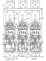
- Figure 10 is a front elevation view of circuit protective device having the cover removed.
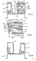
- Figure 11 is a framentary side elevation view of circuit protective' device, with the tripping mechanism shown in its latched position.
- Figure 12 is fragmenary side elevation view of the circuit protective device in Fig. 11, with the plunger of the delatching mechanism shown in its delatching position and the tripping mechanism shown just prior to moving to the tripped position.
- Figure 13 is a fragmentary side elevation view of the circuit protective device in Fig. 11, with the tripping mechanism shown in its tripped position and the plunger of the delatching mechanism shown as moved to its reset position.
- Figure 14 is an end elevation view of the delatching mechanism and one of the step-up transformers of a circuit protective device.
- Figure 15 is a side elevation view of the delatching mechanism shown in Fig. 14.
- Figure 16 is an end elevation view of the ground fault toroid and of a second step-up transformer of a current protective device.
- Figure 1 7 is a side elevation view of trip lever of a circuit protective device.
- Figure 18 is an end elevation view of the trip lever of Fig. 17.
- Figure 19 is a top plan view of the trip cross-bar and its associated tripping and rest members extending therefrom.
- Figure 20 is a side elevation view of the trip cross-bar and associated members shown in Fig. 19.
- Figure 21 is a plan view of the auxiliary cover and rating plug cover assembly of a circuit protective device.
- Figure 22 is a side elevation view of one side of the rating plug of a circuit protective device.
- Figure 23 is a side elevation view of the opposite side of the rating plug of Fig. 22.
- Figure 24 is an isometric view of the safety trip mechanism of the circuit protective device, shown in position relative to the trip lever of which a fragment is shown.
- Figure 25 is a fragmentary side elevation view of a circuit protective device, with the safety trip mechanism shown in the no-trip position.
- Figure 26 is a fragmentary side elevation view of a circuit protective device, with the safety trip mechanism shown in the trip position and the tripping mechanism shown just prior to moving the tripped position.
- Figure 27 is a top plan view of the rating plug cap portion of the rating plug cover assembly of Fig. 21.
- Figure 28 is a bottom plan view of the rating plug cap shown in Fig. 27, with the rating plug shown therein.
- Figure 29 is a section view taken on line 29-29 of Fig. 28.
- A
multi-pole circuit breaker 1 includes an electronic fault sensing andtrip initiating unit 2, adelatching assembly 3, anoperating mechanism 4 which includes a.tripping mechanism 5. - The operating and
tripping mechanisms trip initiating unit 2, anddelatching assembly 3, and other parts of the invention disclosed herein. - Different types of operating and tripping mechanisms may be used with the
electronic unit 2 and delatchingassembly 3 of the invention. - The
operating mechanism 4 is mounted in thecircuit breaker case 6, comprising abase portion 6a and acover portion 6b. Theoperating mechanism 4 includes anoperating assembly 7 connected to move themovable contacts 8 of each pole between a contact open position and contact closed position with reference to the respective stationary contacts 9 of each pole.Movable contacts 8 are conductively connected respectively tocorresponding terminals 10 of each pole at end 11 of thecircuit breaker 1. Stationary contacts 9 are conductively connected respectively to corresponding terminals 11 of each pole at theopposite end 12 of thecircuit breaker 1. - The tripping
mechanism 5 is movable by the operatingassembly 7 to a latched position against the bias of toggle springs 14. When so latched themovable contacts 8 may be moved by the operatingassembly 7 to the contact closed position. Upon occurence of a fault condition sufficient to actuate themagnetic delatching assembly 3, the trippingmechanism 5 is moved from its latched position whereupon the toggle springs 14 cause the breaker to trip thus rapidly moving themovable contacts 8 of each pole to the contact open position to interrupt the circuit. - The electronic fault sensing and
trip initiating unit 2 includes threecurrent transformers cores _terminals current transformer 15, secondary winding 25 forcurrent transformer 16 and secondary winding 26 forcurrent transformer 17. - A
differential transformer 27 is mounted on aframe 28 secured to asupport member 28a of thecircuit breaker 1 over the center pole of the breaker adjacent the end 11.Differential transformer 27 includes a summingtoroid 29,primary windings secondary windings current transformers respective conductors primary windings primary windings transformers respective conductors primary windings secondary windings current transformers respective conductors - The
current transformers transformers primary windings differential transformer 27. Sincecurrent transformers circuit breaker 1, in a three-wire grounded neutral A.C. distribution circuit one of them is inductively connected to the neutral conductor and the other two to the line conductors of the circuit. The primary ofdifferential transformer 27 connected in series with the secondary of the neutral connected current transformer likewise carries the current induced from the neutral conductor while the other two carry the current induced from the two line conductors in such three-wire circuit. The result is that the sum of the currents flowing through theprimaries differential transformer 27 is normally opposite and equal, thus cancelling out to zero. The magnetic flux resulting from such current flow in theprimaries - The
differential transformer 27 also includes a secondary winding 48, connected byconductors primaries current transformers primaries differential transformer 27 are inductively coupled. If the primary winding ofdifferential transformer 27 which is coupled to the neutral conductor carries less current than the sum of the currents flowing in the line conductors, an imbalance of magnetic flux occurs which then induces a voltage signal in secondary winding 48. Such signal is transmitted byconductors circuit breaker 1 and interrupt the circuit. - A fourth primary winding 51 is provided on the summing
toroid 29 ofdifferential transformer 27 for use in four wire circuits. This fourth primary winding 51 is connected at a first terminal toconductor 52 which leads to a firstterminal screw 53 of aterminal block 54, and is connected at a second terminal toconductor 55 which leads to a secondterminal screw 56 onterminal block 54. Theterminal block 54 is mounted on thecover portion 6b ofcircuit breaker case 6, for convenient access from outside of the breaker. In a four wire circuit for which ground fault protection is desired, a separatecurrent transformer 57 is mounted at any convenient location in the vicinity of thecircuit breaker 1, the fourth bus bar or other conductor of the fourth wire system is series connected through thecore 58 of the separatecurrent transformer 57, such series connection through the core becoming the primary winding of such current transformer. A secondary winding 59 is provided on thecore 58 oftransformer 57, and the first and second terminals of such secondary 59 may then be connected respectively to first and second terminal screws 53 and 56 onterminal block 54. When such connection is made, currents flowing through the four wire system-are fed to the summingtoroid 29 ofdifferential transformer 27 through its fourprimary windings differential transformer 27 resulting in a pick-up signal in its secondary winding 48 as described above for a three wire circuit. - The step-up
transformers secondary windings rating adjustment assembly 63, byrespective conductors conductors conductors - The
conductors differential transformer 27 also lead to respective terminals on the ampererating adjustment assembly 63. - Thus, overcurrent faults sensed by
current transformers 1 5" 16 and 17 are fed through step-uptransformers rating adjustment assembly 63, and ground faults sensed bydifferential transformer 27 are also fed to the ampererating adjustment assembly 63. - The ampere
rating adjustment assembly 63 includes aterminal slot 64 in thebase portion 6a of thecircuit breaker case 6 having conductive strips connected to the respective terminals to whichconductors conductors 49 and 50 (from the differential transformer) are connected, and an ampere rating plug 70 having astab portion 71 withconductive strips 72 for contact with corresponding conductive strips of the terminal slot 674 when thestab 71 ofampere rating plug 70 is inserted therein. Theampere rating plug 70 includes fourresistors conductive strips 72, for connection to respective pairs of conductive strips interminal slot 64. Whenampere rating plug 70 is inserted into theterminal slot 64, respective ones of theresistors transformers resistors ampere rating plug 70 is an example, may be provided with resistors of different values to change the ampere rating of the breaker from 2,000 amperes to 1,000 amperes in increments of 200 amperes. That is to say, one rating plug would reduce theampere rating 200 amperes, from 2,000 A. to 1,800 A. A second rating plug would contain resistors of such value that would reduce theampere rating 400 amperes, from 2,000 A. to 1,600 A., and so on. It is of course possible and within the scope of this invention to choose different resistance values to conveniently provide different ampere ratings of a circuit breaker, other than those set forth above as example. - A
circuit board 77 is mounted in thecover portion 6b of thecircuit breaker case 6. Thecircuit board 77 has mounted thereon the electronic solid state components which make up the overcurrent fault trip initiating circuits and the ground fault trip initiating circuits. - Conductor pairs lead to the
circuit board 77 from the connections to the ampererating adjustment assembly 63 as follows: - (a)
Conductor pair transformer 39 to the ampere rating adjusting assembly), - (b)
Conductor pair transformer 40 to the ampere rating adjustment assembly), - (c)
Conductor pair transformer 40 to the ampere rating adjustment assembly), - (d)
Conductor pair differential transformer 27 to the ampere rating adjustment assembly). - The overcurrent fault trip initiating circuits include an input section comprising a rectified power supply, a pick-up stage, a long time delay circuit, a short time delay circuit, an instantaneous trip circuit, and an electronic switching stage to initiate tripping of the circuit breaker.
- The input section includes full wave rectification bridges 86, 87, 88 and 89.
Conductors transformer 39 which is inductively coupled to one phase of the circuit breaker.Conductors transformer 40 which is inductively coupled to a second phase of the circuit breaker.Conductors transformer 41 which is inductively coupled to a third phase of the circuit breaker.Conductors grids 89 fromdifferential transformer 27, in which all three phases (or four in a four wire system) of the circuit breaker serve as primary windings. The ground fault trip initiating circuit will be described in greater detail below. - When the circuit is operating normally under a no-fault condition, a pick-up alternating voltage will be induced in the respective
current transformers transformers bridges capacitor 90 through conductors 91 (leading from bridge 86), 92 (leading from bridge 87), 93 (leading from bridge 88),conductor 94 which leads from respective junctions withconductors capacitor 90. The DC voltage produced acrosscapacitor 90 is proportional to the AC voltage supplied by the step-uptransformers -
Resistors conductor 94, and a four position ampererating adjustment switch 98 is connected toconductor 94 at various settings in relation toresistors position adjustment switch 98 operates by connecting the two poles adjacent whatever adjustment level the switch is set at As shown in the drawing (Figs. 4 and 5), when set at the 100% adjustment level, the two pins on each side of thedesignation 100% are connected which eliminates the switch entirely thus directing current through both of the associatedresistors resistor 96 so current is directed throughresistor 97.Resistor 97 has a relatively higher resistance value thanresistor 96, for example 4.7 Kohms forresistor 97 and 2.7 Kohms forresistor 96. Whenswitch 98 is set at the 80% adjustment level, the two pins on each side of that designation are connected which shorts out resistor 97 (having relatively higher resistance) and directs current through resistor 96 (having relatively lower resistance). Whenswitch 98 is set at the 70% adjustment level, the two pins on each side of that adjustment designation are connected which shorts out both resistors so the current completely bypasses theresistors rectifiers - At normal operating current and with no fault present, a low output from the rectification bridges 86, 87 and 88 leads through
conductors 94 and 95 tocapacitor 90 charging it to a pre-determined voltage. When the ampererating adjustment switch 98 is set at the 80% rating for example, the impressed voltage oncapacitor 90 is about 12 volts. - The output signal is also directed through
resistor 99 andzener diode 100 to circuit ground. A ground current path leads from the components which are circuit ground connected to the circuit ground connections of conductors 101, 102 and 13 leading torectification bridges zener diode 100 is at about 50% of the input. voltage. The voltage drop acrossresistor 99 results in a lowering of the voltage of the emitter of theN-P-N transistor 104 to about 7 volts (as compared to about 12 volts on capacitor 90).Transistor 104 is conducting during normal current no fault operating conditions with a current path through its emitter being directed throughresistor 105 leading to the base oftransistor 106 andresistor 107 leading to the collector oftransistor 106, which is also conducting during normal current no fault conditions.- The current path through the emitter oftransistor 106 leads throughresistor 108 andcommon conductor 109 to circuit ground through aground terminal 110. The capacitor 111 which is in parallel withresistor 108 is charged to a small voltage to stabilize the circuit. - The other leg of the pick-up stage leads from
resistors 967 and 97 and adjustment switch 98 throughconductor 112 to a voltage divider net- work consisting of a variable resistor orpotentiometer 113 andresistors diode 117 is in parallel withresistor 115 to provide temperature compensation for thetransistor 118, the base of which receives an output from the voltage divider network, but which is not conducting during normal current no fault conditions.Resistor 116 leads to circuit ground. - The voltage divider network just described serves in conjunction with the ampere
rating adjustment switch 98 and its associatedresistors transistor 118 begins to conduct, and below which it remains non-conductive. When an overcurrent fault condition occurs in one phase of the circuit and is picked up by the current and step-up transformers which monitor that phase, the DC voltage from the associatedrectification bridge resistor combination potentiometer 113,resistors transistor 118 conductive and thus initiate activation of other components in the long time delay tripping circuit. The reference voltage is set at about 15 volts when the ampererating adjustment switch 98 is set at 70%, at about 17 volts when set at 80%, at about 19.2 volts when set at 90%, and at about 21.3 volts when set at 100%. - The
potentiometer 113 is inserted in the voltage divider network to adjust for any losses and enable fine tuning of the voltage divider to the desired pre-determined reference voltage. - Also while operating at normal current no fault condition, there is a current path from the junction between
resistors conductor 119 andresistor 120 leading to afirst base 121 ofunijunction component 122. Theresistor 120 limits current tounijunction component 122 and serves as a temperature compensator. - When an overcurrent fault condition occurs which is of sufficient magnitude to raise the reference voltage of the network supplying the base of
transistor 118 above the pre-determined voltage levels, at such time thetransistor 118 switches to a conductive state. Current is then drawn through its collector- emitter circuit, resulting in a lowering of the voltage at junction X, betweenresistor 105 and the base of previously conductingtransistor 106. When the voltage on the base oftransistor 106 is lowered, it switches to a non-conductive state. The current path throughresistor 123 is then shunted throughconductor 124 in which capacitor 125 is normally charged throughresistor 123 to somewhat less than 1/2 of the voltage which appears at thefirst base 121 ofunijunction component 122, that is during normal operating no fault conditions at whichtime unijunction 122 is not conducting through itssecond base 126. When the full rectified output is directed tocapacitor 125 throughresistor 123, it charges to about 1/2 of the voltage which appears atbase 121 ofunijunction transistor 122 causingunijunction 122 to change state andcapacitor 125 to discharge. When it changes state, the unijunction begins to conduct through itssecond base 126, thus providing a current path from theemitter 127 ofunijunction 122, through itssecond base 126,resistor 128,common conductor 109 andcircuit ground terminal 110. This provides an input signal to the base oftransistor 129 throughdiode 130driving transistor 129 into saturation as described further hereinbelow. Theunijunction transistor 122 then resets. - The components consisting of
resistors capacitor 125,unijunction 122 anddiode 130 comprise a relaxation oscillator circuit which delivers a series of oscillations or pulses to a pulse generator circuit at a pulse rate which is essentially linearly related to the input voltage of the fault condition being sense. Thus, for a low magnitude fault condition the pulse rate is slower than for a high magnitude fault and in each case the pulse rate is proportional to the magnitude of the input voltage of the fault. The function of thediode 130 is to isolate the relaxation oscillator state from the pulse generator stage. - The pulse generator circuit includes
transistors resistors capacitor 136 anddiode 137. Under normal operating no fault conditions, a low level output is supplied totransistor 131 throughresistor 134 connected to the base oftransistor 131 and throughresistor 135 connected to its collector.Transistor 131 is biased into saturation throughresistor 134. At such time,transistor 129 is non-conducting.Capacitor 136 is charged thorughresistor 133 to the input voltage of the circuit. - When a fault condition occurs of sufficient magnitude to generate a series of oscillations or pulses from the relaxation oscillator through
unijunction transistor 122, base drive is provided totranisistor 129 driving it into saturation on occurrence of each pulse. The charge oncapacitor 136 throughresistor 133 is nearly equal to positive input voltage, which under a fault condition of said 150% overcurrent would be about 25 volts positive on the side of thecapacitor 136 which is connected toresistor 133. The resulting voltage on the other end ofcapacitor 136 is driven to nearly negative input voltage. This negative potential applied to the base of normally conductingtransistor 131 causes it to change state and become non-conducting. This causes the voltage on the collector oftransistor 131 to rise to nearly input voltage, which constitutes the output of the pulse generator circuit. - While the collector voltage of
transistor 131 is high, base drive is provided throughresistor 132 to the base oftransistor 129 which maintainstransistor 129 in a saturated conducting state. During this interval of time, thecapacitor 136 is being charged throughresistor 134. When the charge oncapacitor 136 reaches about one volt positive, thetransistor 131 begins to conduct again which lowers the collector voltage resulting in less drive being applied to': the base oftransistor 129 causing it to abruptly change from a conducting to a non-conducting state. Thecapacitor 136 continues to charge, from nearly input voltage negative, to about 1.0 volt positive where the change in state oftransistors transistor 129 changes to its original non-conducting state andtransistor 131 to its original saturated or conducting state, thecapacitor 136 then continues to charge throughresistor 133 up to about the input voltage of the circuit. The cycle is prepared on receipt of the next oscillation or pulse fromunijunction component 122 of the relaxation stage on the base oftransistor 129. - It will be noted that
capacitor 136 charges from input voltage negative to input voltage positive, and the change of state of transistors 129 (from saturated to non-conducting) and 131 (from non-conducting to saturated) occurs at about half way between these extremes. The pulse width of the pulse generator output is therefore essentially independent of voltage, although the amplitude of the pulse output and the rate of the pulse output are linearly related to the input voltage of the fault condition being sensed. - The output pulses from the collector of
transistor 131 in the pulse generating stage are fed to an integrating stage which consists ofresistors 138 through 146,capacitors N-P-N transistors 150, programmable unijunction transistor 151 anddiodes transistor 131 are applied to thecapacitor 149 throughresistor 140 andpotentiometer 141. Thediode 154 betweenresistor 141 andcapacitor 149 serves as a low leakage component to prevent leakage discharge of the capacitor during that part of the cycle when the pulse is not present. - The charge on the
capacitor 149 increases until it reaches a value which is determined by the voltage on the gate of the unijunction transistor 151. When the voltage charge on thecapacitor 149 and on theanode 157 of unijunction 151 is about 0.6 volts greater than the voltage on thegate 158 of the unijunction transistor 151, the capacitor discharges intoresistor 145 which is in turn applied through conductor 159-and diode 160 to the gate of the electronic switch, SCR (silicon controlled rectifier) 161. The SCR 161 then turns on and energizes a tripping mechanism described in detail hereinbelow to trip'the circuit breaker. - The voltage on the
gate 158 of unijunction transistor 151 is a reference voltage determined bytransistor 150,zener diode 153, resistor 142 and resistor 144. During the time that a pulse is being applied from the pulse generator, thetransistor 150 is saturated receiving its base drive throughresistor 138. During this time that the pulse is being applied from the pulse generator, a reference voltage is applied to thegate 158 of unijunction transistor 151 through a voltage dividingnetwork comprising resistors 142, 144, 146,N-P-N transistor 150, andzener diode 153. This reference voltage is dependent on the input voltage and compensates for non-linearity of the amplitude of charging voltage relative to the time it takes for thecapacitor 149 to charge. Thus over a voltage range considerable error could result in chargingcapacitor 149 to a fixed reference voltage. For example, if the charging voltage is reduced by a factor of four the time delay is increased by more than a factor of four. In order to minimize this error the reference voltage supplied to thegate 158 of unijunction transistor 151 is made variable by the reference voltage network described herein, and it varies depending on the input voltage. The following graph illustrates the ideal reference voltage against input voltage by curve A, and curve B (comprising two straight lines B1 and BZ) illustrates the actual reference voltage generated by the reference voltage network described herein: -

- The variable reference voltage supplied to
gate 158 of unijunction transistor 151 also serves to minimize leakage from thecapacitor 149 though the unijunction transistor 151. If the voltage on theanode 157 of unijunction 151 increases by more than 0.6 volts above the voltage on thegate 158, the unijunction transistor 151 changes state from very high impedance (open circuit and non-conducting) to low impedance (closed circuit and conducting). Thus, as long as the reference voltage on thegate 158 is kept at more than 0.6 volts above the voltage on thecapacitor 149 and theanode 157 of unijunction transistor 151, leakage of the charge on the capacitor will be minimized. - During the
time capacitor 149 is being charged by receiving a pulse from the pulse generator stage throughresistor 140 andpotentiometer 141, there is of course no problem of leakage so the reference voltage orgate 158 of unjunction 151 may be established during application of the charging pulse at a pre-determined level to permit unijunction 151 to change state from non-conducting to conducting when the magnitude and duration of the fault current being sensed reaches a pre- determined level. However, during the interval between pulses from the pulse generating stage leakage could occur fromcapacitor 149 through unijunction 151, so it is desirable to raise the reference voltage on thegate 158 during such interval whencapacitor 149 is not being charged, and lower it to the pre-determined level whencapacitor 149 is being charged. - Such variation of the reference voltage level is accomplished as follows. When a pulse is being supplied to
capacitor 149 from thecollector 131 in the pulse generating stage, throughresistor 140 andpotentiometer 141, base drive is also being supplied to switchingtransistor 150 throughresistor 138 driving it into saturation. A current path is then established fromconductor 112, throughresistor 146, resistor 144,zener diode 153, resistor 142, the collector emitter circuit of transistor 15C andcircuit ground terminal 110. This current path through the voltage dividing net- work described results in establishing a voltage at junction Y at whatever pre-determined level desired for operation of the long time delay tripping circuit. Such reference voltage at junction Y is applied to thegate 158 of unijunction 151 during the time that capacitor 149 is being charged by a pulse received from the pulse generator stage. - During the invervals between pulses, or when no pulses are being supplied by the pulse generator stage, there is no base drive to switching
transistor 150 and it changes state to non-conducting. The voltage at junction Y andgate 158 of unijunction 151 is accordingly raised above the pre-determined reference level, and the gate voltage of unijunction 151 approaches the level of input voltage of the circuit limited by zener diode 156. The unijunc- . tion transistor 151 is thus maintained at a very high impedance state to minimize leakage during all times when no pulse is being received from the pulse generator stage and thecapacitor 149 is not being charged. - When the magnitude and duration of the pulses from the pulse generating stage charge the
capacitor 149 to more than about 0.6 volts above the reference voltage ongate 158 of unijunction transistor 151, the unijunction transistor changes state and conducts dischargingcapacitor 149 throughresistor 145, conductor 159, diode 160, gating SCR 161 into conduction and delivering a tripping voltage to the tripping mechanism more fully described hereinbelow to trip the breaker and interrupt the circuit. - The long time delay tripping circuit described above produces a time delay which is inversely proportional to the square of the applied voltage. To produced such a time delay the gate voltage applied to unijunction transistor 151 must be a function of applied voltage. The reference voltage network described above provides such a variable reference voltage which varies as a function of applied voltage.
- When an overcurrent fault occurs, the bus bars, circuit breaker, panelboard, and associated components become hot. It is therefore desirable to maintain a charge on
capacior 149 after an overcurrent fault clears and no further pulses are being received from the pulse generator stage. The charge oncapacitor 149 should be allowed to slowly dissipate over a time period which corresponds with the time it takes for the bus bars and other components to cool. Thus, if another overcurrent fault occurs before they cool, a partial charge will remain oncapacitor 149 which shortens the time delay period before it will iniitate tripping of the breaker. - To accomplish this result, a
diode 152 and aresistor 162 are connected in series throughconductor 163 withcapacitor 149. Thus when no further pulses are being received throughresistors conductor 163 through which the charge oncapacitor 149 can leak away at a controlled rate, the rate being pre-determined by the values selected for thediode 152 andresistor 162. The pre-determined leakage rate is chosen to correspond to the cooling rate of physical components of the circuit breaker and its associated electrical distribution system. - Since a charge is maintained on
capacitor 149 for a pre-determined time after a fault clears and the output is no longer received from the pulse generating stage, some means must be provided to keep the reference voltage on thegate 158 of unijunction transistor 151 at a level of 0.6 volts or more above the voltage charge oncapacitor 149 which is also the voltage applied to theanode 157 of unijunction transistor 151. Otherwise, the unijunction would change state and initiate tripping even though the initial overcurrent fault condition had been cleared. - The reference voltage on
gate 158 is maintained at such level of 0.6 volts or more above the voltage oncapacitor 149 when the input voltage of the long time delay circuit drops below the retained voltage oncapacitor 149 bycapacitor 147 in conjunction withresistor 143 and diode 155.Capacitor 147 is charged throughresistor 143 when the integrating stage is receiving an output from the pulse generating stage. The resistor 144 limits the rate of charging ofcapacitor 147 such that it does not interfere with the function of the reference voltage network described above. The change oncapacitor 147 is held by diode 155, which is series connected withcapacitor 147 and positioned to block discharge thereof.Capacitor 147 is series connected to junction Y (connected to the terminal ofgate 158 of unijunction 151), and diode 155 is cathode connected in series with junction Y. Thus, when a condition occurs whereby the input voltage to the long time delay circuit drops to a lower value than the retained chage oncapacitor 149, such as when an overcurrent fault has cleared, there is a charge oncapacitor 147 which is pre- determined (by selection of component values) at a level above that of the retained charge oncapacitor 149. Such voltage appears at junction Y andgate 158 of unijunction 151 for at least as long as the time it takes for the charge oncapacitor 149 to leak away through its leakage control circuit ofresistor 162 anddiode 152. The unijunction transistor 151 is thus prevented from changing state which would cause the breaker to trip during such time as a controlled leakage charge still remains oncapacitor 149 and while no fault condition is being sensed by the long time delay circuit. - A short time delay trip initiating circuit is provided to sense overcurrent faults of high magnitude and initiate tripping of the breaker with less time delay than that provided by the long time delay circuit described above.
- The short time delay circuit includes a pick-up stage and a voltage dependent time delay stage. Both the pick-up stage and time delay stage are adjustable by means of a resistor network and switch.
- The pick-up circuit includes
resistors 164, 165,166,167,168,169,170,171,172,173, 174, 175 and,transistors diodes 180 and 181,capacitors - At voltage levels below the pre-determined pick-up voltage of the short time delay circuit,
transistor 179 is conducting throughresistor 172 series connected to its collector and throughresistor 173 leading toground terminal 185 connected in series to its emitter. Thetransistor 179 receives base drive through resistor 171 and variable resistor orpotentiometer 170. Thecapacitor 183 which is connected across the emitter and collector circuit oftransistor 179 is not able to charge above the 1.0 volt while this transistor is conducting. There is therefore no output from the pick-up stage of such voltage levels. - When a high overcurrent fault occurs above the pre-determined pick-up voltage, base drive to
transistor 178 reaches the level which causes it to change state and begin to conduct through it collector emitter circuit. This results in a low voltage at junction Z, the base terminal connection oftransistor 179, causing it to change state and become non-conducting. The collector voltage oftransistor 179 then rises to approximately the regulated voltage level which will cause the relaxation oscillator stage of the short time delay circuit to begin operating, as provided between theresistor 172 andcapacitor 183 to prevent charging the capacitor through thisresistor 172. Thecapacitor 183 is charged from the input voltage through a resistance network in the relaxation oscillator stage as also explained more fully below. - The relaxation oscillator stage consists of
resistors capacitors 183 and 9, andprogrammable unijunction 189. Thecapacitor 183 is charged from the input voltage which appears on conductor-112 leading from the ampere rating adjustment switch 98 (described above), throughresistors adjustment switch assembly 190 comprising a resistance network which sets both the pick-up level of the short time delay circuit and the time delay for each pick-up level. -
Switch 190 is four position slide switch which includes two sets of five pins each, thefirst set 191 controlling the pick-up level and thesecond set 192 controlling the maximum time delay setting for each pick-up level. The switch operator is movable to four positions, and in each position it connects the two adjacent pins of thefirst set 191 and the two adjacent pins of thesecond set 192. Thus, the pick-up levels may be set for an overcurrent fault of 200% at the setting designated 2X or 200%; 400% at the setting designated 4X or 400%; 500% at the setting designated 5X or 500%; and 600% overcurrent at the setting designated 6X or 600%. - At the 2X or 200% setting, pins 191 a and 191 b in the first set are connected and
pins 192a and 192b in the second set are also connected by the switch operator. At this setting, all threeresistors conductor 193 and controlled by the first pin set 191 are shorted out; andresistors 187 and 188 controlled by the second pin set 192 are shorted out. - At the 4X or 400% setting,
resistors resistor 187 in the circuit controlled by the second pin set 192. - At the 5X or 500% setting,
resistor 166 is shorted out, leavingresistors 165 and 167 in the circuit controlled by the first pin set 191; andresistor 187 shorted out, leaving resistor 188 in the circuit controlled by the second pin set 192. - At the 6X or 600% setting, all three
resistors resistors 187 and 188 are in the circuit controlled by the second pin set 192. - For purposes of illustration and not by way of limitation, the resistors controlled by the first pin set 191 may have the following relative values:
- Resistor 165 - 68 Kohms
- Resistor 166 - 82 Kohms
- Resistor 167 - 150 Kohms
- The resistors controlled by the second pin set may have the following relative values:
- Resistor 187 - 1.6 Meg. Ohms
- Resistor 188 - 2.5 Meg Ohms
- Thus, at the 2X or 209% setting for pick-up at 200% overcurrent fault condition, there would be no resistance in the circuit from either pin set 191 or 192 of the short time delay pick-up
adjustment switch assembly 190, althoughresistors capacitor 183 from the input voltage carried onconductor 112. The time delay established by the second pin set 192 at the 2X or 200% setting would be approximately 155 milli-seconds maximum for a fault condition of 200% overcurrent. The time delay decreases proportionately with the increase in percentage of overcurrent above the 200% level, or above whatever the setting may be. - At the 4X or 400% setting for pick-up at 400% overcurrent fault condition, there would be 150 Kohms resistance in the circuit controlled by the first pin set 191 to set the pick-up level at 400%; and there would be 1.6 Meg. Ohms plus 150 Kohms or a total of 218 Kohms in the circuit controlled by the first pin set 191 to set the pick-up level at 500%; and there could be 2.4 Meg Ohms in the circuit controlled by the second pin set 192 to set the time delay at about 124 milliseconds.
- At the 6X or 600% setting for pick-up at 600% overcurrent fault condition, there would be 68 Kohms plus 28 Kohms plus 150 Kohms (i.e. resistors 165, 166 and 167) in the circuit controlled by the second pin set 192 to set the time delay at about 140 milliseconds. The time delay is inversely proportional to the level of overcurrent.
- On occurrence of an overcurrent fault condition at or above the short time delay pick-up setting chosen, a voltage signal is transmitted on
conductor 193 through the resistance net-work established by the first pin set 191 of the pick-upadjustment switch 190, and to the base oftransistor 178 throughresistor 164 driving it into saturation whereupon it begins to conduct causingtransistor 179 to also change state as described above. Its collector voltage approaches the regulated voltage level established for the relaxation oscillator stage to begin operating. - The relaxation oscillator stage begins to operate when the voltage charge on capacitor 183 (received from
input conductor 112 throughresistors gate 195 ofunijunction transistor 189. When the voltage oncapacitor 183 reaches 0.6 volts thus making theanode 196 ofunijunction 189 0.6 volts positive relative to itsgate 195, theunijunction transistor 189 changes state and becomes conductive.Capacitor 183 then discharges through resistor 177, throughdiode 197, gating SCR 161 into conduction causing the breaker to trip. - An instantaneous trip initiating circuit is provided for very high overcurrent faults, consisting of a resistor in series with a
zener diode 199 and atrigger diode 200, connected to the input DC supply byconductor 112. When the input onconductor 112 reaches about 125 volts, the reverse breakdown point ofzener diode 199 is reached allowing current to pass to triggerdiode 200 which in turn passes current throughconductor 201 to trigger SCR 161 in conduction to trip the circuit breaker without any time delay. - A ground fault trip initiating circuit is also provided for protection of the breaker and distribution system against ground faults of a magnitude which would not be sensed and picked up by the other trip initiating circuits. The ground fault trip circuit includes a pick-up stage and a time delay stage.
- Ground faults are sensed by the
differential transformer 27 and are fed to therectification bridge 89 from the secondary winding 48 throughconductors rating adjustment plug 63, and throughconductors conductor 202 and resistor 203 on occurrence of a ground fault sensed bydifferential transformer 27 and picked up in its secondary winding 48. - A ground fault would be sensed by
differential transformer 27 when one of the phases of the distribution circuit becomes grounded on the load side of the breaker, whereupon a portion of the current would return to the source through a ground path rather than through the neutral conductor of the system. The currents, and magnetic flux, atdifferential transformer 27 would thus be imbalanced, resulting in net magnetic flux to be picked up in the secondary winding 48. - The rectified ground fault output from
bridge 89 is carried tostorage capacitor 90 through resistor 203,diode 204, the pick-upadjustment switch 98, andconductors 94 and 95.Capacitor 90 leads to circuit ground, and ground terminal connection 205 ofbridge 89 completes the ground circuit. - The resistor 203 in combination with
zener diode 206 limits the voltage from the ground fault which is applied tostorage capacitor 90 and to the ground fault pick-up and delay circuits. This is done to prevent the short time delay trip initiating circuit from responding to the voltage that would appear onstorage capacitor 90 if the voltage were not limited, and to allow a substantially constant charging voltage to be applied to the time delay capacitor 207. - The pick up stage of the ground fault trip initiating circuit includes
transistors resistors 203, 210 through 222, capacitors 223 and 207.Resistor 215 is a variable resistor. The pick-up voltage level on the ground fault trip initiating circuit is determined by the voltage dividing network consisting .ofresistor 214,variable resistor 215,resistors gate 224 of theunijunction transistor 225 throughconductor 226 andresistor 221. The pick-up voltage level on the ground fault trip initiating circuit is adjustable internally at the factory by changing the setting ofvariable resistor 215, but it is not externally adjustable by the user. - Operation of the ground fault trip initiating circuit is as follows. Below the pick-up voltage level,
transistor 209 is conducting andtransistor 208 is non-conducing. Whentransistor 209 is conducting, a current path extends from the DC power supply input throughconductors 94 and 95,transistor 104,conductors resistor 218 to the base oftransistor 208, throughresistor 219 to the collector oftransistor 209, throughresistor 220 and then tocircuit ground terminal 229. -
Transistor 208 is non-conducting at conditions below the pick-up voltage level of the ground fault trip initiating circuit. - While
transistor 209 is conducting, a low voltage of about 1.0 to 1.5 Volts is present at its collector and at the junction XX between the collector oftransistor 209 and the cathode of the diode 230 which is anode connected to the time delay capacitor 207. Thus, while such low voltage is present at junction XX, capacitor 207 cannot be charged to more than approximately 1.0 to 1.5 volts since current flowing through theresistor network - When a ground fault voltage signal appears at the output of
bridge 89 which exceeds the set pick-up level established by the voltage divider network ofresistors transistor Transistor 208 begins to receive base drive throughresistors resistor 218 through its collecton to emitter circuit, throughresistor 220 andcircuit ground terminal 229. A low voltage results at junction YY between the collector oftransistor 208 andresistor 218, causingtransistor 209 to change state and become non-conducting. At such time, the collector voltage oftransistor 209 rises from about 1.0 to 1.5 volts to about 7 volts, which likewise raises the voltage at junction XX to about 78 volts. The capacitor 207 can then be charged throughresistors delay adjustment switch 231, since the high voltage at junction XX blocks the previous path through diode 230. - The ground fault time
delay adjustment switch 231 is a four position slide switch to adjust the response time of the tripping mechanism on occurrence of a ground fault. At a setting of 1 as shown on the drawing the time delay may be for example 100 milliseconds; at a setting of .2 it may be for example 200 milli- seconds; at a setting of .3 it may be for example 300 milliseconds and at a setting of .5 it may be for example 500 milliseconds. - The switch circuit includes
resistor resistor 211 may be 680 Kohms,resistor 212 may be 1.5 Megohms, and resistor 213 may be 620 Kohms. - When the operator of
switch 231 is set at the .1 position, pins 231 a and 231 b are connected, which shorts outresistors resistors 212 and 213 leavingresistor 211 in the switch circuit to provide a switch circuit resistance of 680 Kohms in the example given for a time delay of 200 milliseconds. When set at the .3 position pins 231c and 231d are connected, which shorts outresistor 212 leavingresistors 211 and 213 in the switch circuit to provide switch circuit resistance of 680 Kohms plus 620 Kohms for a total of 1.3 Megohms which provides a time delay of 300 milliseconds in the example given. When set at the .5 position, pins 231d and 231e are connected, which inserts all threeresistors -
Resistor 210 is in the capacitor charging circuit in addition to any or all of theresistors - Capacitor 207 is connected to the
anode 232 ofunijunction transistor 225. When the voltage charge on capacitor 207 (and thus on theanode 232 of unijunction 225) reaches the level at which it is about 0.6 volts above the voltage on thegate 224 ofunijunction 225, the unijunction transistor changes state from very high impedance (resembling an open circuit) to low impedance. Capacitor 207 then discharges intoresistor SCR 235 into conduction, and also discharges intoresistor 236 to gate SCR 161 into conduction which initiates tripping of the breaker. - The
SCR 235 is connected to a solenoid described later herein which actuates visual indication means to indicate that the breaker tripped due to a ground fault condition. - Internal ground fault
trip indication terminals terminal block 54. A separate electronic monitoring assembly having an indicator lamp, of the type described in Patent No. 3,943,409 assigned to the assignee of the present application, can be connected to terminals 237a and 238a for external or remote indication of tripping due to a ground fault condition. - The ground fault indicator solenoid is energized by the discharge of
capacitor 239 throughterminal 238 switched bySCR 235. Thecapacitor 239 is charged from the ground faultdifferential transformer 27 throughbridge 89 and resistor 203 upon occurrence of a ground fault. After the appropriate delay, electronic switch SCR 161 is triggered by a pulse from the discharge of capacitor 207. This same pulse also triggersSCR 235 into conduction and allowscapacitor 239 to discharge through the ground fault tripindicator solenoid SCR 235, andcircuit ground terminal 240. - The externally mounted electronic monitoring assembly having an indicator lamp to indicate a trip due to a ground fault condition requires a pulse of a certain magnitude and duration, such as 32 volts with a duration of at least one millisecond. This is provided by combining the signal appearing on
internal terminal 238 with a pulse which appears oninternal terminal 237. The pulse atterminal 237 is provided by the circuit consisting ofresistors capacitor 243 anddiode 244. Thecapacitor 243 is charged through about 24 volts for example upon the occurrence of a ground fault, the charging voltage selected depending on the relative values of the other components in the circuit. After the appropriate delay (dependent on the setting oftime delay switch 231 and the magnitude of the ground fault) the ground fault trip occurs andSCR 235 is triggered into conduction forcing the positive side ofcapacitor 243 to ground. Since the capacitor discharge path is blocked bydiode 244, the output toterminal 237 will be approximately -24 volts in the example given for purposes of illustration. The voltage onterminal 238 charged bycapacitor 239 in the embodiment described herein is +24 volts, so the potential difference betweenterminals - The electronic switch 161 is triggered into conduction by voltage signals transmitted from either the long time delay trip circuit, the short time delay trip circuit, the instantaneous trip circuit or the ground fault trip circuit to the
gate 245 of SCR 161. A capacitor 246 and resistor 247 are provided in parallel with the cathode - gate circuit of SCR 161 for the purpose of suppressing transients and noise which might otherwise trigger the SCR 161 into conduction. - The tripping energy is supplied to the tripping coil controlled by SCR 161 by
storage capacitor 90 discharging throughconductor 94, energizing the tripping coil and through SCR 161 to circuit ground throughcircuit ground terminal 248. - The circuit breaker includes means for a user to test the various trip initiating circuits when desired to determine that the circuits are in proper operating condition. Such means includes
test terminals 251 through 258. One series of tests will enable the user to conveniently test the pick-up levels of the long time delay trip initiating circuit, the short time delay trip initiating circuit and the ground fault trip initiating circuit. A second series of tests will enable the user to conveniently test the pick-up levels of the long time delay trip initiating circuit, the short time delay trip initiating circuit and the ground fault trip initiating circuit. A second series of tests will enable the user to conveniently test the time delay section of the circuitry. - An appropriate testing device may be connected to a conventional 120 AC power supply, and will provide a DC output of from 0 to 150 volts. It includes a terminal insert corresponding to the ampere
rating adjustment plug 70, which is inserted into theterminal slot 64 in the base of the circuit breaker being tested. The ampere rating adjustment plug 70 is removed from the breaker and inserted into a corresponding terminal slot in the testing device, so the same ampere rating of the breaker is applied to the testing device. The testing device includes a pair of output conductors having connecting terminals for connecting to corresponding terminals at appropriate test points in the electronic circuits to be tested for the purpose of applying an appropriate test voltage to the circuits being tested. Additional leads and terminal connections are provided to short out the circuits not being tested, and to measure the response at selected test points in the circuit which is being rested. The testing device as such is not a part of the present application, and any test device capable of providing a DC voltage of between 0 volts to 150 volts DC to a circuit, and measuring the response voltage at selected test points of the circuit being tested, could be made to operate for purposes of testing the circuits. The test portion of the circuitry which is included as part of the invention covered by the present application is that which is physically incorporated in the circuitry of the circuit breaker itself. - The short time delay trip initiating circuit includes a
test point terminal 251 connected between the collector oftransistor 179,resistor 172 and diode 181. - The long time delay trip initiating circuit includes a
test point terminal 252 connected between the collector oftransistor 106,resistor 107 anddiode 164. - The ground fault trip initiating circuit includes a
test point terminal 253 connected between the collector oftransistor 209,resistor 219 and diode 230. - A voltage
input test terminal 254 is connected tostorage capacitor 90 to provide test voltages to the short time delay and long time delay circuits respectively as they are being tested. - A short-to-
ground test terminal 256 is provided, connected between thegate 245 of electronic switch SCR 161 and the output conductors of the various trip initiating circuits, to short the electronic switch out to ground and prevent actual tripping of the circuit breaker during the short time delay test. The time between sensing such faults and tripping is so short (e.g. less than one second), so it is desirable for measuring response during a test of the short time delay circuit to avoid actual tripping of the breaker. - A circuit
ground test terminal 257 is provided for connecting to ground terminal 248 of the circuit. A ground terminal lead from the testing device is connected to test terminal 257 to complete the circuit which begins atinput test terminal 254 which receives an input test voltage through a lead from the testing device, or at a secondinput test terminal 258 described in the next paragraph. - A second voltage
input test terminal 258 is provided to supply an appropriate test Voltage to the ground fault trip initiating circuit.Test terminal 258 is connected to the ground fault trip initiating circuit between resistor 203,diode 204, and the ground fault indicator solenoid.Test terminal 258 is also connected toterminal 238 which receives the discharge fromcapacitor 239 as it is applied to the ground fault indicator solenoid on occurrence of a ground fault of tripping magnitude and duration. During a simulated ground fault for test purposes, the testing device supplies the simulated ground fault voltage toterminal 258 which therectification bridge 89 normally supplies toterminal 238 on occurrence of an actual ground fault condition in the distribution circuit protected by the circuit breaker of this invention. - The testing means operates as follows. After connecting the terminal insert of the testing device in
terminal slot 64 of the circuit breaker, and the ampere rating adjustment plug 70 in a corresponding terminal slot of the testing device, the voltage output lead of the testing device is connected toterminal 254 of the circuit breaker and the ground terminal lead of the testing device is connected toterminal 257 of the circuit breaker. - The testing means in accordance with this invention operates as follows. After connecting the terminal insert of the testing device in
terminal slot 64 of the circuit breaker, and the ampere rating adjustment plug 70 in a corresponding terminal slot of the testing device, the voltage output lead of the testing device is connected toterminal 254 of the circuit breaker and the ground terminal lead of the testing device is connected toterminal 257 of the circuit breaker. - To test the pick-up stages of the long time delay and short time delay circuits, the lead from the testing device which measures response from the circuit being tested, is connected either to test terminal 251 (short time delay circuit) or test terminal 252 (long time delay circuit) depending on which circuit is being tested, and short-out leads are also connected to the test terminals of the pick-up stages of the other two circuits which are not at the time being tested. Thus, if the pick-up stage of the short time delay circuit is being tested,
test terminal 252 in the long time delay circuit and test terminal 253 in the ground fault circuit would be shorted out by connecting the short-out leads thereto. - When the pick-up state of the long time delay circuit is being tested,
test terminal 251 in the short time delay circuit and test terminal 253 in the ground fault circuit could be shorted out by connection thereto of the short-out leads. - When the pick-up stage of the ground fault circuit is being tested,
test terminal 251 in the short time delay circuit and test terminal 252 in the long time delay circuit are shorted out by connecting the short-out leads to such terminais. - The first test may be of the pick-up stage of the long time delay circuit. A simulated overcurrent voltage of about 15 volts or above is applied to test terminal 254, whereupon a transition from low voltage (e.g. 1.5 volts) to high voltage (e.g. 7 volts) should appear at
test terminal 252 if the pick-up stage of the long time delay circuit is operating properly. - The next test may be of the pick-up stage of the time delay circuit. A simulated overcurrent voltage of about 26 volts or above is applied to test terminal 254, whereupon a transition from low voltage (e.g. 1.5 volts) to high voltage (e.g. 7 volts) should appear at
test terminal 251 if the pick-up stage of the short time delay circuit is operating properly. - A third test may be of the pick-up stage of the ground fault time delay circuit. A simulated ground fault voltage of about 18 volts is applied to test terminal 258, whereupon a transition from low voltage (e.g. 1.5 volts) to high voltage (e.g. 7 volts) should appear at
test terminal 253 if the pick-up stage of the ground fault stage is operating properly. - The voltage levels applied to the input test terminals to simulate an overcurrent fault of sufficient magnitude to activate each circuit will. depend on the setting of the ampere rating' adjustment switch 98-. In the examples of voltages given above for purposes of illustration, switch 98 may be at the 70% setting.
- The fourth test may be of the time delay stage of the long time delay circuit. With test terminals 251 (in the short time delay circuit) and 253 (in the ground fault circuit) shorted out as described above, an input voltage is applied from the testing device to test terminal 254 at selected voltages above the trip level of about 15 volts (at a 70% setting of ampere rating adjustment switch 98). At 15 volts, a time delay of about 500 seconds for example may occur before tripping occurs (or before a gating signal is applied to SCR 161) if the time delay section of the long time delay circuit is working properiy. When a higher voltage such as 30 volts is applied to test terminal 254, the time delay should be reduced to about 250 seconds, i.e. inversely proportional to the increase in voltage applied, if the circuit is working properly.
- The fifth test may be of the time delay stage of the short time delay circuit. With test terminals 252 (tong time delay circuit) and 253 (ground fault circuit) shorted out, an input test voltage of about 40 volts may be applied to test terminal 251. If the short time delay stage is operating properly, the breaker will trip within less than one second. The
test terminal 256 may be shorted to ground to prevent triggering of SCR 161 and actual tripping of the breaker. The elapsed time may then be measured between application of the voltage ontest terminal 251 and appearance of a triggering signal ontest terminal 256. If the elapsed time is greater than instantaneous, and less than about one second, when a test voltage is applied of a magnitude which simulates that of an overcurrent fault which would initiate operation of the short time delay circuit, the time delay stage of this circuit is functioning properly. The elapsed time will vary depending on the setting of short timedelay adjustment switch 190. - The sixth test may be of the time delay stage of the ground fault circuit. With test terminals 251 (short time delay) and 252 (long time delay) shorted out, an input test voltage of about 30 volts for example may be applied to test terminal 258. If the ground fault time delay stage is operating properly, the elapsed time between application of the test voltage and appearance of a tripping signal on test terminal 256 (or actual tripping of the breaker) should be greater than an instantaneous trip and less than about one second. The elapsed time will of course vary depending on the setting of the ground fault
time delay switch 231. - When a trip initiating signal is received at the gate of electronic switch SCR 161, it is triggered into
conduction allowing capacitor 90 to discharge into atrip coil 300 of themagnetic delatching assembly 3. Thedelatching assembly 3 includes aplunger type armature 301 slidingly positioned intrip coil 300, normally biased outwardly to the unlatching position byhelical compression spring 302. Apermanent magnet 303, mounted onferrous magnet frame 304, in conjunction with a softiron flux concentrator 305, holdsarmature 301 inwardly oftrip coil 300 to the latching position. When the gap between theend 306 of theflux concentrator 305 and theshank 307 ofarmature 301 is closed, the magnetic field of thepermanent magnet 303, enhanced byflux concentrator 305, has sufficient force to hold thearmature 301 inwardly against the bias ofspring 302. The magnetic flux of thepermanent magnet 303 flows in a direction from thenorth pole 308 of thepermanent magnet 303, through themagnet frame 304, through theshank 307 ofarmature 301, through theflux concentrator 305 and to thesouth pole 309 of thepermanent magnet 303. Anon-magnetic screw 310 holds thepermanent magnet 303 andflux concentrator 305 in place on themagnet frame 304. - When a trip initiating signal gates SCR 161 into conduction, the current flow through
coil 300 is such that the magnetic field generated by such current flow opposes that of the permanent magnet, thus weakening its magnetic attraction force sufficiently to enable the bias ofspring 302 to overcome such attracting force thus movingarmature 301 outwardly to its unlatching position. As shown in the drawing . (FIG. 3), the current incoil 300 may be considered as flowing towards the viewer on the left-hand side of the figure and away from the viewer on the right-hand side. Thus, in accordance with the right-hand rule for determining direction of magnetic flux in an electromagnet, the flux path through the core of thecoil 300 may be considered to be from the end adjacent thepermanent magnet 303 to the end adjacent thehelical compression spring 302. - Since the direction of magnetic flux of the energized coil is opposite the direction of magnetic flux of the permanent magnet, the respective magnetic fields diminish in
strength enabling spring 302 to movearmature 301 outwardly to contactfirst end portion 311 ofrocker arm 312.Rocker arm 312 then pivots onpivot pin 313 causing itssecond end portion 314 to striketrip lever 315.Trip lever 315 then moves rearwardly drawinglatch pin 316 fromlatch member 317, causing the circuit breaker to trip. - When the breaker trips, the
cradle 318 pivots clockwise as shown in the drawing (FIG. 13) and itsrearward end portion 319 strikes theforward end portion 320 ofspring lever 321, causing it to rotate acommon trip shaft 322 in the unlatching direction. Three spring levers 321 are mounted oncommon trip shaft 322, one for each pole of the breaker. Whentrip shaft 322 is rotated by movement of thefirst spring lever 321 in the unlatching direction, the other twospring levers 321 of the other two poles of the breaker are also rotated causing therearward end 323 to strike corresponding trip levers 315. There are also threetrip levers 315, one positioned in each pole of the breaker, each having alatch pin 316 engaging acorresponding latch member 317. When respective spring levers 321 strike corresponding trip levers 315 moving them rearward, their corresponding latch pins 317 disengage fromrespective latch members 317 of each pole causing all poles of the breaker to trip whenever a fault of tripping magnitude and duration is sensed by the breaker. - A reset
spring lever arm 324 is mounted oncommon trip shaft 322, being positioned to contact thefirst end portion 311 ofrocker arm 312 from the forward side, i.e. the side opposite from that which is contacted by the head ofarmature 301. Whentrip shaft 322 is rotated in the unlatching position causing all poles of the breaker to trip,reset arm 324 is also being rotated to contactend portion 311 ofrocker arm 312 moving it and armature 301 rearwardly to the reset position. In such position, the head ofarmature 301 compressesspring 302 and the shank ofarmature 301 is received withincoil 300 until its rearward free end comes into close proximity with theflux concentrator 305. At such time,coil 300 is no longer energized and the magnetic field ofpermanent magnet 303 is thus strong enough to retainarmature 301 in the reset or unlatched position until such time as the breaker is moved to the contact closed position again and another fault occurs to reset the cycle. - A back-up or protective thermal tripping
mechanism 350 is provided to trip the circuit breaker if the load conductors (internal bus bars 21, 22 and 23) become over-heated due to such causes as a poor electrical connection to the load or an unusually high ambient temperature. The electronic trip initiating circuits are input voltage dependent, and would not sense certain conditions which cause temperature rise in the breaker and distribution system but which do not necessarily affect input voltage. - The back-up thermal tripping
mechanism 350 includes threebimetal strip members 351 bolted respectively to internal bus bars 21, 22 and 23, by connectingbolts 352, at locations which position thefree end portions 353 of eachbimetal strip member 351 for engagement respectively with a correspondingthermal release tab 354 projecting laterally from each of the three trip levers 315. When an over-temperature condition (not input voltage related) occurs of sufficient temperature to cause tripping of the breaker by the back-up thermal trippingmechanism 350, such as for example a load bus bar temperature of 130°C, the bimetal strip member in the particular pole involved will deflect until it contacts the correspondingthermal release tab 354 of its pole movingtrip lever 315 rearwardly until itslatch pin 316 disengages fromlatch member 317 of that pole, causing the breaker to trip as described above. - The internal ground fault trip indicator assembly includes a plunger type ground
fault indicator armature 360 mounted in the bore of a groundfault indicator coil 361 and normally biased outwardly of thecoil 361 by ahelical compression spring 362. When thearmature 360 is pushed inwardly of thecoil 361, theshank end 363 ofarmature 360 narrows the gap between it and thepole end 364 of aflux concentrator 365 of soft iron, which enhances the attraction force of the magnetic field of apermanent magnet 366 mountedadjacent flux concentrator 365 on an iron frame 367. Anon-magnetic screw 368 secures the assembly to a structural member of thecircuit breaker 1. When the gap between theshank end 363 ofarmature 360 and pole end 364 offlux concentrator 365 is narrowed, the attraction force of the enhanced magnetic field of thepermanent magnet 366 is sufficient to hold thearmature 360 inwardly ofcoil 361 against the bias ofspring 362. - Upon occurrence of a ground fault of sufficient magnitude to initiate tripping of the breaker, ground
fault indicator coil 361 is energized as a result ofcapacitor 239 discharging throughterminal 238,coil 361 andSCR 235. The magnetic field produced by such discharge throughcoil 361 opposes the magnetic field produced by thepermanent magnet 366 andflux concentrator 365, in substantially the same manner as described above with respect totrip coil 300 andarmature 301 of thedelatching assembly 311. The magnetic field of thepermanent magnet 366 is thus weakened until the bias ofspring 362 is able to overcome the attraction force of the permanent magnet, enabling thespring 362 to move thearmature 360 outwardly of thecoil 361. The appearance of ground faulttrip indicator armature 360 in such outward extended position visually indicates that thecircuit breaker 1 has tripped because of a ground fault condition. - To reset, the
armature 360 is pushed inwardly against the bias ofspring 362 until the gap has narrowed sufficiently for the attraction force of thepermanent magnet 366 to overcome the biasing force of thespring 362, thus holding the ground faulttrip indicator armature 360 inwardly ofcoil 361 until another ground fault occurs of sufficient magnitude to trip the breaker. - The circuit breaker includes a shunt trip assembly, comprising a
resistor 370 inconductor 371 connected at one end tofirst terminal 372 oftrip coil 300 and adiode 373 inconductor 374 anode connected tosecond terminal 375 oftrip coil 300. The opposite end ofconductors terminals terminal block 54. An external power source, such as a 120 volt one ampere alternating current supply, may then be connected toterminals -
Resistor 370 limits current to thetrip coil 300 to the magnitude required for generating a magnetic field incoil 300 in opposition to the field ofpermanent magnet 303 which is sufficient to allowspring 302 tobias trip armature 301 outwardly to the delatching position, as more fully described above. The current path from the external power source through the shunt trip assembly of this invention is throughterminal 376 onterminal block 54 of thecircuit breaker 1,conductor 371,resistor 370,first terminal 372 oftrip coil 300, thetrip coil 300, itssecond terminal 375,conductor 374, the anode ofdiode 373, the cathode ofdiode 373, terminal 377 onterminal block 54 back to the external power source. - The adjustment switches previously described including ampere
rating adjustment switch 98, short time delay pjck-up adjustment switch 1909, and ground fault timedelay adjustment switch 231, include respectiveoperating slide members cover 2 of thecircuit breaker 1 for external access. Users are thus able to set each of the adjustment switches 98, 190 and 231 to the respective positions described previously from the front of the circuit breaker without removing the cover, or disassembling any parts, or disconnecting the breaker from its installation. - Appropriate markings are also provided on the exterior of the
cover 2, opposite each adjustment setting or position of each of the adjustment switches 98, 190 and 231. - The ampere
rating adjustment switch 98 includes for example, theexternal markings 70%, 80%, 90%, and 100%, opposite the respective positions ofoperating slide member 380 to achieve a substantially precise pick-up level of the breaker at 70%, 80% 90% and 100% respectively of the ampere rating of the breaker established by whatever one of the plurality of ampere rating plugs 70 has been inserted interminal slot 64 of thecircuit breaker 1 as described previously herein. Thus, the user may set the ampere rating of the breaker externally by inserting the desired ampere rating plus 70, and he may also adjust the pick-up level externally by movingoperating slide member 380 to the setting for the percentage of such ampere rating which the user desires. It is understood that for purposes of the invention, the percentages and magnitudes used herein are illustrative and are not intended to limit the scope of the invention. Other percentages and magnitudes may be established if desired. - The short time delay pick-up
adjustment switch 190 includes, for example, theexternal markings 200%, 400%, 500% and 600% as shown in the drawing (FIG. 5) of the breaker used herein to describe the invention. The marking 200% is opposite the position of operatingslide member 381 ofswitch 190 which establishes a pick-up level for the short time delay trip initiating circuit at an overcurrent fault condition of 200%. The marking 400% is opposite the switch position which establishes a pick-up level at a 400% overcurrent fault condition; the marking 500% opposite switch position for a 500% overcurrent fault condition; and marking 600% opposite switch position for a 600% overcurrent fault condition. Again, these settings are illustrative and do not limit the scope of the invention. Other settings and percentages may be established within the scope of this invention. Such settings and percentage levels of overcurrent fault conditions adjustable on the external cover of the breaker are substantially accurate and precise. When a user sets theswitch 190 at the 200% marking he knows that the short time delay trip initiating circuit will initiate tripping at substantially precisely a 200% overcurrent fault condition, and so on at the 400%, 500% and 600% markings. The time delay adjustments (controlled byswitch 190 and simultaneously adjusted when the overcurrent fault setting is adjusted) are also substantially precise enabling the user to set at a substantially precise level both the overcurrent pick-up level and time delay for each overcurrent setting externally of the breaker by merely setting a switch at the desired marking. - The ground fault time
delay adjustment switch 231 includes for example the markings ".1 sec", ".2 sec", ".3 sec", and ".5 sec", as shown in the drawing (FIG. 5) for purposes of illustration. At the ".1 sec" setting ofswitch 231, the ground fault trip initiating circuit will initiate tripping at substantially precisely one tenth of a second after occurrence of a ground fault of a magnitude above the level established by the ampere rating plug 70 being used at the time. At the ".2 sec" setting ofswitch 231, the ground fault trip initiating circuit will initiate tripping at substantially precisely two-tenths of a second; at the ".3 sec" setting, it will initiate tripping at substantially precisely three-tenths of a second; and at the ".5 sec" setting, it will initiate tripping at substantially five-tenths of a second, after occurrence of a ground fault above the magnitude established by the other external controls (ampere rating plug 70 and ampere rating adjustment switch 98). A user may therefore easily and conveniently set the time delay for various magnitudes of ground fault conditions at substantially precise and determinable time periods set forth on the outside ofcover 6b of the breaker by merely setting theswitch 231 at the position opposite the desired time delay period. A separate meter or other measuring device is not needed, nor are special tools required to accomplish the adjustments and settings described herein.. - The circuit breaker includes a
safety trip mechanism 400 to trip the breaker if the rating plug cover assembly 6c is not in place. Such mechanism includes apush button 402 having ashaft portion 402b and ahead portion 402a, mounted for reciprocal movement between a trip and no-trip position, in aport 403 provided in thecircuit breaker cover 6b at a location adjacent theslot 64 in which theampere rating plug 70 is inserted. The heat portion 501 a is of larger cross-sectional dimension than theshaft portion 402b. - A generally L-shaped
safety trip lever 404 is pivotally mounted onpivot shaft 405 to a portion of themagnet frame 304, and includes a horizontally extendingfirst leg 406 and a vertically extendingsecond leg 407. Thefirst leg 406 includes a free end offsetplanar tab portion 408 which is positioned for engagement by saidpush button 402 when said button is moved inwardly toward the no-trip position. Thesecond leg 407 includes a freeend projecting tab 409 for contact with a laterally extendingsafety trip tab 410 of thebreaker trip lever 315, when thesafety trip lever 404 is pivotally moved to the trip position. - The
safety trip lever 404 is biased toward the trip position byhelical extension spring 411, anchored at one end to a laterally extendingpivot arm 412 ofsafety trip lever 404 and at the other end to pivotpin 313 on whichrocker arm 312 is pivotally mounted. Aflange 413 extends at substantially a right angle from the free end portion of laterally extendingarm 412. The pivot shaft is mounted through aligned apertures 414 (in the flange 413) and 415 (in a corresponding portion of the spaced apartfirst leg 406 of the safety trip lever 404). The pivot shaft also extends through corresponding apertures in spaced apartlegs magnet frame 304. - When rating plug
cover assembly 401 is removed,push button 402 is uncovered and free to move from the no-trip position to the trip position. Thespring 411 biases thesafety trip lever 404 toward the trip position wherein the vertically extendingsecond leg 407 moves into engagement with thebreaker trip lever 315 causing the breaker to trip. At such time the horizontally extendingfirst leg 406 is moved into bearing engagement againstpush button 402 moving it from the no-trip to the trip position. The circuit breaker cannot be reset until thepush button 402 is moved in the opposite direction back to the no-trip position, which occurs when the-rating plug cover assembly 6c is put in place after insertion of anampere rating plug 70. - The ampere
rating cover assembly 401 includes arating plug 418 and arating plug cover 423 having an outer jacket orcasing 419. Cover 423 is attached to auxiliary cover 6c. Cover 6c engages thepush button 402 of the safety trip mechanism pushing it inwardly to the no-trip position. The ampere rating of the particular rating plug is printed on thetop wall 422 of 418 and centrally located thereon. When therating plug 70 is inserted intoterminal slot 64 to make the ampererating adjustment assembly 63 operative as described previously herein, therating plug cap 418 is placed over therating plug 70. A projectingedge portion 420 ofrating plug cap 418 engages thepush button 402 of thesafety trip mechanism 400 pushing it inwardly to the no-trip position. Therating plug cap 418 includes arecess 421 to receive the outwardly projecting portion of rating plug 70 therein whencap 418 is put in place over theplug 70. The ampere rating of the particular rating plug is printed on thetop wall 422 ofcap 418 and centrally located thereon. - The
outer casing 419 ofcover assembly 401 includes acentral aperture 423 through which the ampere rating ofplug 70 printed on thetop wall 422 thereof is visible whenouter casing 419 is put in place overrating plug cap 418. Theouter casing 419 is secured by screws to auxiliary cover 6(c), which is proved on cover 6(b) for access to theterminal block 54 and to the groundfault trip indicator 360. The outer jacket orcasing 419 retains therating plug cap 418 in place until it is desired to remove theampere rating plug 70.
Claims (4)
Applications Claiming Priority (2)
| Application Number | Priority Date | Filing Date | Title |
|---|---|---|---|
| US05/886,962 US4208689A (en) | 1978-03-15 | 1978-03-15 | Circuit breaker having an electronic fault sensing and trip initiating unit |
| US886962 | 1978-03-15 |
Publications (3)
| Publication Number | Publication Date |
|---|---|
| EP0015924A4 EP0015924A4 (en) | 1980-07-08 |
| EP0015924A1 EP0015924A1 (en) | 1980-10-01 |
| EP0015924B1 true EP0015924B1 (en) | 1984-05-16 |
Family
ID=25390155
Family Applications (1)
| Application Number | Title | Priority Date | Filing Date |
|---|---|---|---|
| EP79900294A Expired EP0015924B1 (en) | 1978-03-15 | 1979-10-12 | Circuit breaker having an electronic fault sensing and trip initiating unit |
Country Status (7)
| Country | Link |
|---|---|
| US (1) | US4208689A (en) |
| EP (1) | EP0015924B1 (en) |
| AU (1) | AU524908B2 (en) |
| CA (1) | CA1131337A (en) |
| DE (1) | DE2966978D1 (en) |
| MX (1) | MX149071A (en) |
| WO (1) | WO1979000768A1 (en) |
Families Citing this family (13)
| Publication number | Priority date | Publication date | Assignee | Title |
|---|---|---|---|---|
| US5166887A (en) * | 1988-03-31 | 1992-11-24 | Square D Company | Microcomputer-controlled circuit breaker system |
| US5095398A (en) * | 1990-02-12 | 1992-03-10 | Square D Company | Electrical circuit breaker protection device |
| GB9510173D0 (en) * | 1995-05-19 | 1995-07-12 | Garrard David E | Safety device for electric power distribution systems for buildings |
| US6560084B1 (en) * | 1999-11-05 | 2003-05-06 | Siemens Energy & Automation, Inc. | Circuit breaker having programmable amplifier |
| US7518475B2 (en) * | 2007-07-24 | 2009-04-14 | Eaton Corporation | Electrical switching apparatus, circuit interrupter and method of interrupting overcurrents of a power circuit |
| DE102011081773A1 (en) * | 2011-08-30 | 2013-02-28 | Siemens Aktiengesellschaft | Method for operating an electrical device and circuit breaker |
| US11108225B2 (en) | 2017-11-08 | 2021-08-31 | Eaton Intelligent Power Limited | System, method, and apparatus for power distribution in an electric mobile application using a combined breaker and relay |
| US11052784B2 (en) | 2017-11-08 | 2021-07-06 | Eaton Intelligent Power Limited | Power distribution unit and fuse management for an electric mobile application |
| US11070049B2 (en) | 2017-11-08 | 2021-07-20 | Eaton Intelligent Power Limited | System, method, and apparatus for power distribution in an electric mobile application using a combined breaker and relay |
| US11368031B2 (en) | 2017-11-08 | 2022-06-21 | Eaton Intelligent Power Limited | Power distribution and circuit protection for a mobile application having a high efficiency inverter |
| US11689010B2 (en) | 2019-02-22 | 2023-06-27 | Eaton Intelligent Power Limited | Coolant fitting promoting turbulent flow |
| WO2021009217A2 (en) | 2019-07-15 | 2021-01-21 | Eaton Intelligent Power Limited | Power distribution and circuit protection for a mobile application having a high efficiency inverter |
| CN113571381B (en) * | 2021-08-23 | 2024-06-21 | 广东沃德精密科技股份有限公司 | Iron stand and hook stranding equipment |
Citations (1)
| Publication number | Priority date | Publication date | Assignee | Title |
|---|---|---|---|---|
| US3786311A (en) * | 1973-01-02 | 1974-01-15 | Gen Electric | Circuit breaker and static trip circuit therefor |
Family Cites Families (5)
| Publication number | Priority date | Publication date | Assignee | Title |
|---|---|---|---|---|
| FR1407271A (en) * | 1964-06-20 | 1965-07-30 | Electronique Et D Automatique | Electrical circuit protection device |
| US3803455A (en) * | 1973-01-02 | 1974-04-09 | Gen Electric | Electric circuit breaker static trip unit with thermal override |
| US3996499A (en) * | 1974-09-09 | 1976-12-07 | Westinghouse Electric Corporation | Zener diode effect on long acceleration module |
| US4038618A (en) * | 1976-04-12 | 1977-07-26 | I-T-E Imperial Corporation | Circuit breaker having thermal and solid state trip means |
| US4090156A (en) * | 1976-04-12 | 1978-05-16 | I-T-E Imperial Corporation | Circuit breaker having solid state and thermal-magnetic trip means |
-
1978
- 1978-03-15 US US05/886,962 patent/US4208689A/en not_active Expired - Lifetime
-
1979
- 1979-03-14 WO PCT/US1979/000153 patent/WO1979000768A1/en not_active Ceased
- 1979-03-14 DE DE7979900294T patent/DE2966978D1/en not_active Expired
- 1979-03-15 CA CA323,514A patent/CA1131337A/en not_active Expired
- 1979-03-15 AU AU45127/79A patent/AU524908B2/en not_active Ceased
- 1979-03-15 MX MX176935A patent/MX149071A/en unknown
- 1979-10-12 EP EP79900294A patent/EP0015924B1/en not_active Expired
Patent Citations (1)
| Publication number | Priority date | Publication date | Assignee | Title |
|---|---|---|---|---|
| US3786311A (en) * | 1973-01-02 | 1974-01-15 | Gen Electric | Circuit breaker and static trip circuit therefor |
Also Published As
| Publication number | Publication date |
|---|---|
| AU4512779A (en) | 1979-09-20 |
| DE2966978D1 (en) | 1984-06-20 |
| EP0015924A4 (en) | 1980-07-08 |
| CA1131337A (en) | 1982-09-07 |
| AU524908B2 (en) | 1982-10-07 |
| EP0015924A1 (en) | 1980-10-01 |
| WO1979000768A1 (en) | 1979-10-04 |
| MX149071A (en) | 1983-08-18 |
| US4208689A (en) | 1980-06-17 |
Similar Documents
| Publication | Publication Date | Title |
|---|---|---|
| US4208693A (en) | Circuit breaker having an electronic fault sensing and trip initiating unit | |
| US4209817A (en) | Circuit breaker having an electronic fault sensing and trip initiating unit | |
| US4213165A (en) | Circuit breaker having an electronic fault sensing and trip initiating unit | |
| US4215328A (en) | Circuit breaker having an electronic fault sensing and trip initiating unit | |
| EP0012754B1 (en) | Circuit breaker having an electronic fault sensing and trip initiating unit | |
| US3803455A (en) | Electric circuit breaker static trip unit with thermal override | |
| US4060844A (en) | Solid state tripping circuit | |
| CA1131296A (en) | Ground fault circuit interrupter | |
| US4208689A (en) | Circuit breaker having an electronic fault sensing and trip initiating unit | |
| US4223365A (en) | Auto resetting switchgear trip indicator circuits | |
| CA1132239A (en) | Ground fault apparatus and protection system | |
| US7692903B2 (en) | Apparatus and method for controlling a circuit breaker trip device | |
| US3786311A (en) | Circuit breaker and static trip circuit therefor | |
| US3924160A (en) | Circuit breaker with detachably connected fault simulator | |
| US4208690A (en) | Circuit breaker having an electronic fault sensing and trip initiating unit | |
| US4866557A (en) | Low level voltage programmable logic control | |
| US3899717A (en) | Ground fault detectors | |
| US3668471A (en) | Device for detection and control of leakage and excessive current flow | |
| US4897756A (en) | Add-on ground fault module | |
| US3852660A (en) | Circuit breaker fault simulator | |
| EP0333412B1 (en) | Circuit breakers test device | |
| US3723815A (en) | Electronic circuit protective device | |
| CA2036032A1 (en) | Electrical circuit breaker protection device | |
| US4096366A (en) | Means for detecting a loss of vacuum in vacuum-type circuit interrupters used in polyphase a.c. vacuum circuit breaker | |
| US3683237A (en) | Adjustable solid state overload relay |
Legal Events
| Date | Code | Title | Description |
|---|---|---|---|
| PUAI | Public reference made under article 153(3) epc to a published international application that has entered the european phase |
Free format text: ORIGINAL CODE: 0009012 |
|
| 17P | Request for examination filed | ||
| AK | Designated contracting states |
Designated state(s): DE FR GB |
|
| GRAA | (expected) grant |
Free format text: ORIGINAL CODE: 0009210 |
|
| AK | Designated contracting states |
Designated state(s): DE FR GB |
|
| REF | Corresponds to: |
Ref document number: 2966978 Country of ref document: DE Date of ref document: 19840620 |
|
| ET | Fr: translation filed | ||
| PLBI | Opposition filed |
Free format text: ORIGINAL CODE: 0009260 |
|
| 26 | Opposition filed |
Opponent name: AEG-TELEFUNKEN AKTIENGESELLSCHAFT, BERLIN UND FRAN Effective date: 19850209 |
|
| PLBN | Opposition rejected |
Free format text: ORIGINAL CODE: 0009273 |
|
| STAA | Information on the status of an ep patent application or granted ep patent |
Free format text: STATUS: OPPOSITION REJECTED |
|
| 27O | Opposition rejected |
Effective date: 19860522 |
|
| PGFP | Annual fee paid to national office [announced via postgrant information from national office to epo] |
Ref country code: GB Payment date: 19910215 Year of fee payment: 13 |
|
| PGFP | Annual fee paid to national office [announced via postgrant information from national office to epo] |
Ref country code: FR Payment date: 19910321 Year of fee payment: 13 |
|
| PGFP | Annual fee paid to national office [announced via postgrant information from national office to epo] |
Ref country code: DE Payment date: 19910327 Year of fee payment: 13 |
|
| PG25 | Lapsed in a contracting state [announced via postgrant information from national office to epo] |
Ref country code: GB Effective date: 19920314 |
|
| GBPC | Gb: european patent ceased through non-payment of renewal fee | ||
| PG25 | Lapsed in a contracting state [announced via postgrant information from national office to epo] |
Ref country code: FR Effective date: 19921130 |
|
| PG25 | Lapsed in a contracting state [announced via postgrant information from national office to epo] |
Ref country code: DE Effective date: 19921201 |
|
| REG | Reference to a national code |
Ref country code: FR Ref legal event code: ST |