EP0003079B1 - Infra red light emissive devices - Google Patents
Infra red light emissive devices Download PDFInfo
- Publication number
- EP0003079B1 EP0003079B1 EP78300858A EP78300858A EP0003079B1 EP 0003079 B1 EP0003079 B1 EP 0003079B1 EP 78300858 A EP78300858 A EP 78300858A EP 78300858 A EP78300858 A EP 78300858A EP 0003079 B1 EP0003079 B1 EP 0003079B1
- Authority
- EP
- European Patent Office
- Prior art keywords
- light emissive
- red light
- active region
- infra
- layer
- Prior art date
- Legal status (The legal status is an assumption and is not a legal conclusion. Google has not performed a legal analysis and makes no representation as to the accuracy of the status listed.)
- Expired
Links
- 229910052785 arsenic Inorganic materials 0.000 claims description 30
- 239000000758 substrate Substances 0.000 claims description 22
- 239000006104 solid solution Substances 0.000 claims description 17
- 239000000463 material Substances 0.000 claims description 12
- 239000000203 mixture Substances 0.000 claims description 10
- 229910005542 GaSb Inorganic materials 0.000 claims description 9
- 239000010410 layer Substances 0.000 description 27
- 230000003287 optical effect Effects 0.000 description 11
- 239000011149 active material Substances 0.000 description 7
- 239000000969 carrier Substances 0.000 description 6
- 238000010276 construction Methods 0.000 description 6
- 239000004065 semiconductor Substances 0.000 description 5
- 229910000673 Indium arsenide Inorganic materials 0.000 description 4
- 150000001875 compounds Chemical class 0.000 description 4
- 230000000694 effects Effects 0.000 description 4
- RPQDHPTXJYYUPQ-UHFFFAOYSA-N indium arsenide Chemical compound [In]#[As] RPQDHPTXJYYUPQ-UHFFFAOYSA-N 0.000 description 4
- WPYVAWXEWQSOGY-UHFFFAOYSA-N indium antimonide Chemical compound [Sb]#[In] WPYVAWXEWQSOGY-UHFFFAOYSA-N 0.000 description 3
- 238000000407 epitaxy Methods 0.000 description 2
- OKTJSMMVPCPJKN-UHFFFAOYSA-N Carbon Chemical compound [C] OKTJSMMVPCPJKN-UHFFFAOYSA-N 0.000 description 1
- 238000007796 conventional method Methods 0.000 description 1
- 229910002804 graphite Inorganic materials 0.000 description 1
- 239000010439 graphite Substances 0.000 description 1
- 230000012447 hatching Effects 0.000 description 1
- 238000002347 injection Methods 0.000 description 1
- 239000007924 injection Substances 0.000 description 1
- 239000011229 interlayer Substances 0.000 description 1
- 238000004943 liquid phase epitaxy Methods 0.000 description 1
- 238000004020 luminiscence type Methods 0.000 description 1
- 238000000034 method Methods 0.000 description 1
- 238000012986 modification Methods 0.000 description 1
- 230000004048 modification Effects 0.000 description 1
- 230000005855 radiation Effects 0.000 description 1
Images

Classifications
-
- H—ELECTRICITY
- H10—SEMICONDUCTOR DEVICES; ELECTRIC SOLID-STATE DEVICES NOT OTHERWISE PROVIDED FOR
- H10H—INORGANIC LIGHT-EMITTING SEMICONDUCTOR DEVICES HAVING POTENTIAL BARRIERS
- H10H20/00—Individual inorganic light-emitting semiconductor devices having potential barriers, e.g. light-emitting diodes [LED]
- H10H20/80—Constructional details
- H10H20/81—Bodies
- H10H20/822—Materials of the light-emitting regions
- H10H20/824—Materials of the light-emitting regions comprising only Group III-V materials, e.g. GaP
-
- H—ELECTRICITY
- H01—ELECTRIC ELEMENTS
- H01S—DEVICES USING THE PROCESS OF LIGHT AMPLIFICATION BY STIMULATED EMISSION OF RADIATION [LASER] TO AMPLIFY OR GENERATE LIGHT; DEVICES USING STIMULATED EMISSION OF ELECTROMAGNETIC RADIATION IN WAVE RANGES OTHER THAN OPTICAL
- H01S5/00—Semiconductor lasers
- H01S5/30—Structure or shape of the active region; Materials used for the active region
- H01S5/32—Structure or shape of the active region; Materials used for the active region comprising PN junctions, e.g. hetero- or double- heterostructures
- H01S5/323—Structure or shape of the active region; Materials used for the active region comprising PN junctions, e.g. hetero- or double- heterostructures in AIIIBV compounds, e.g. AlGaAs-laser, InP-based laser
-
- H—ELECTRICITY
- H10—SEMICONDUCTOR DEVICES; ELECTRIC SOLID-STATE DEVICES NOT OTHERWISE PROVIDED FOR
- H10D—INORGANIC ELECTRIC SEMICONDUCTOR DEVICES
- H10D62/00—Semiconductor bodies, or regions thereof, of devices having potential barriers
- H10D62/80—Semiconductor bodies, or regions thereof, of devices having potential barriers characterised by the materials
- H10D62/85—Semiconductor bodies, or regions thereof, of devices having potential barriers characterised by the materials being Group III-V materials, e.g. GaAs
- H10D62/852—Semiconductor bodies, or regions thereof, of devices having potential barriers characterised by the materials being Group III-V materials, e.g. GaAs being Group III-V materials comprising three or more elements, e.g. AlGaN or InAsSbP
-
- H—ELECTRICITY
- H10—SEMICONDUCTOR DEVICES; ELECTRIC SOLID-STATE DEVICES NOT OTHERWISE PROVIDED FOR
- H10H—INORGANIC LIGHT-EMITTING SEMICONDUCTOR DEVICES HAVING POTENTIAL BARRIERS
- H10H20/00—Individual inorganic light-emitting semiconductor devices having potential barriers, e.g. light-emitting diodes [LED]
- H10H20/80—Constructional details
- H10H20/81—Bodies
- H10H20/811—Bodies having quantum effect structures or superlattices, e.g. tunnel junctions
Definitions
- This invention relates to infra-red light emissive devices, and in particular to such devices having active light emissive regions of the ternary solid solution In (Sb,As) and related multicomponent (quarternary or higher) solid solutions.
- Light emissive devices have been made that had an active light emissive region of In (Sb,As) grown epitaxially upon an In As substrate.
- a problem with this type of construction is that the addition of InSb or InAs to form a solid solution has the effect of changing the lattice spacing. Therefore a graded interlayer was necessary between the active region and the substrate, but even this did not entirely remove the strain from the active region which was relatively heavily dislocated.
- GaSb has a higher band gap than In (Sb,As), and therefore if a device is made that has a p-n junction formed in a layer of lattice matched In (Sb,As) epitaxially grown upon a GaSb substrate, the heterojunction formed between the epitaxial material and the substrate will confine minority carriers injected across the p-n junction towards the substrate. This confinement of minority carriers is also present at the heterojunctions of heterostructure lasers based on (AI,Ga) As, but the heterojunction in the (AI,Ga) As device has the added advantage that it also provides optical confinement because the higher band-gap material has a lower refractive index. The converse is true in the case of a heterojunction between lattice matched In (Sb,As) and GaSb, with the result that such a heterojunction does not provide the optical waveguiding properties desired particularly for laser action.
- the present invention relates to infra-red light emissive devices in which the active material of the device is In (Sb,As) that is lattice matched with a GaSb substrate directly or indirectly supporting the active material and in which the active material is flanked upon at least one side with a lattice matched layer of (AI,Ga) Sb that has a composition providing it with a refractive index less than that of the active material.
- the active material of the device is bounded on at least one side by a heterojunction that provides not only minority carrier confinement but also optical confinement.
- the invention is applicable not only to infra-red light emissive devices whose active material consists of the ternary In (Sb,As) solid solution, but also to those whose active material consist of quarternary and higher solid solutions based on In (Sb,As) and also having a lattice spacing matched with that of GaSb.
- GaSb has the same lattice constant as a particular compound of In (Sb,As), approximately In (Sb 0.1 As 0.9 ), therefore In (Sb o .,As o . 9 ) grown on a GaSb substrate is substantially strain free.
- the rate of increase in lattice spacing is for instance much more rapid than that produced by adding AI As to Ga As to form (AI,Ga) As. This shows why the growth of In (Sb,As) upon an In As substrate is much more difficult than growing (AI,Ga) As upon a substrate of Ga As.
- Ga Sb has the same lattice constant as a particular point on the In (Sb,As) line corresponding approximately to In (Sb o.1 As 0.9 ). Therefore substantially strain free In (Sb 0.1 As 0.9 ) can be grown upon a Ga Sb substrate.
- a Ga Sb substrate 20 of one conductivity type is provided, and then the material of layers 21 and 22 is grown epitaxially upon the substrate 20.
- Layer 21 has the same conductivity type as the substrate while layer 22 is arranged to have the opposite conductivity type in order to form a p-n junction between them.
- the growth may be performed by the conventional methods of compound semiconductor material epitaxy.
- the actual value of the emission wavelength may be shifted by going from the ternary In (Sb,As) solid solution to a quaternay or higher solid solution by increasing the proportion of In Sb and adding a further compound semiconductor material in sufficient quantity to restore the lattice spacing to its original value matching that of Ga Sb.
- the rate of change of lattice spacing and of band gap provided by adding a certain proportion of for instance Ga As to In (Sb,As) is the same as adding that proportion of Ga As to In As.
- the effect of adding Ga As to In (Sb,As) is to a first approximation given by a translation of the (Ga,ln) As curve so that its In As end lies on the appropriate part of the In (Sb,As) curve.
- the In (Sb,As) curve is not so steep at its lower end as the top end of the (Ga,ln)As curve. Therefore, by increasing the proportion of In Sb in In (Sb,As) above In (Sb 0.1 As 0.9 ) and then adding sufficient Ga As to restore the lattice spacing to the In (Sb 0.1 As 0.9 ) value, it can be seen that the band gap is reduced and hence the emission wavelength increased.
- the device of Figure 2 may employ multicomponent, quaternary or higher, solid solution epitaxial layers 21 and 22 in order to provide a wavelength of emission greter or less than that of the ternary In (Sb,As) composition with a lattice spacing matching that of Ga Sb.
- This multicomponent solid solution will be one having a lattice spacing matched with that of Ga Sb and based upon the ternary In (Sb, As) system.
- Ga Sb has a higher band gap than In (Sb,As) and therefore the heterojunction formed between the substrate 20 and layer 21 will serve to confine minority carriers. For some applications it may therefore be advantageous similarly to confine minority carriers on the opposite side of the p-n junction by the use of an additional layer (not shown in Figure 2) of Ga Sb on top of layer 22.
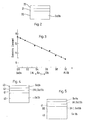
- Figure 3 depicts the variation of optical frequency dielectric constant (equal to the square of the refractive index) for different compositions in the (Al, Ga)Sb solid solution.
- the material bounding the active region In order to provide optical confinement at a heterojunction the material bounding the active region must have a refractive index less than that of the active region, preferably about 1% less. Therefore by adding AI Sb to Ga Sb it is possible to reduce the refractive index to an acceptable value. Typically this will occur in the region of (Al 0.6 Ga 0.4 )Sb.
- (AI,Ga) Sb appears to be more stable than (AI,Ga)As with respect to atmospheric attack, and it is found that (Al 0.6 Ga 0.4 )Sb is stable in air at room temperature.
- Figure 4 depicts a laser which embodies the invention in a preferred form and which is functionally analogous with the single heterostructure (A1,Ga)As laser.
- the laser is grown by epitaxy upon a Ga Sb substrate 40 and includes two, or optionally three, epitaxial layers 41, 42 and 43.
- Layer 41 has the opposite conductivity type to that of the substrate 40, and is made of material having the same lattice spacing as the substrate and it is made of ln(Sb,As) or of a multicomponent, quaternary or higher, solid solution based on ln(Sb,As).
- Layer 42 has the same conductivity type as layer 41, and is made of (A1,Ga)Sb containing a sufficient proportion of AI Sb to reduce ist refractive index beneath that of layer 41 so as to provide the requisite amount of optical confinement in addition to minority carrier confinement.
- Layer 43 has the same conductivity type as layer 42 and is an optional capping layer of Ga Sb which may be provided to protect the underlying layer 42 from atmospheric attack. This will be the more necessary if layer 42 contains a particularly large proportion of AI Sb which would make it more vulnerable to atmospheric attack. In this construction the heterojunction formed between the substrate 40 and layer 41 merely provides electrical confinement whereas that between layers 41 and 42 provides both electrical and optical confinement.
- Figure 5 depicts a laser which embodies the invention in an alternative preferred which is functionally analogous with the double heterostructure(AI,Ga)As laser.
- This is essentially similar to that previously described with reference to Figure 4, but includes an additional layer 50 of (Al, Ga)As of the same conductivity type as the substrate 40 which is located between the substrate and layer 41 which in this instance may have either conductivity type.
- This layer 50 is of a composition providing it with a refractive index the desired amount less than that of layer 41 to provide the requisite optical guidance. In this way electrical and optical confinement is provided at both the heterojunctions flanking the active region provided by layer41.
Landscapes
- Physics & Mathematics (AREA)
- Condensed Matter Physics & Semiconductors (AREA)
- General Physics & Mathematics (AREA)
- Electromagnetism (AREA)
- Optics & Photonics (AREA)
- Semiconductor Lasers (AREA)
- Led Devices (AREA)
Description
- This invention relates to infra-red light emissive devices, and in particular to such devices having active light emissive regions of the ternary solid solution In (Sb,As) and related multicomponent (quarternary or higher) solid solutions. Light emissive devices have been made that had an active light emissive region of In (Sb,As) grown epitaxially upon an In As substrate. A problem with this type of construction is that the addition of InSb or InAs to form a solid solution has the effect of changing the lattice spacing. Therefore a graded interlayer was necessary between the active region and the substrate, but even this did not entirely remove the strain from the active region which was relatively heavily dislocated.
- In an article entitled 'Electron-beam-pumped semiconductor laser utilizing multilayer Gal-xlnxAsl.ySbyheterostructures' appearing in the Soviet Journal of Quantum Electronics, Volume 6 No. 1 January 1976
pages 50 to 53 by S. A. Bondar et al there is a reference to the possibility of growing lattice matched Ga1-xInxAs1-1Sbysolid solutions on substrates of GaSb and InAs. Some work in this field is also reported by L. M. Dolgi- nov et al in an article entitled 'Luminescence and stimulated' emission from GaxIn1-xAsySb1-y appearing in the Soviet Journal of Quantum Electronic, Volume 6 No. 4 April 1976 pages 507 to 508. - GaSb has a higher band gap than In (Sb,As), and therefore if a device is made that has a p-n junction formed in a layer of lattice matched In (Sb,As) epitaxially grown upon a GaSb substrate, the heterojunction formed between the epitaxial material and the substrate will confine minority carriers injected across the p-n junction towards the substrate. This confinement of minority carriers is also present at the heterojunctions of heterostructure lasers based on (AI,Ga) As, but the heterojunction in the (AI,Ga) As device has the added advantage that it also provides optical confinement because the higher band-gap material has a lower refractive index. The converse is true in the case of a heterojunction between lattice matched In (Sb,As) and GaSb, with the result that such a heterojunction does not provide the optical waveguiding properties desired particularly for laser action.
- The present invention relates to infra-red light emissive devices in which the active material of the device is In (Sb,As) that is lattice matched with a GaSb substrate directly or indirectly supporting the active material and in which the active material is flanked upon at least one side with a lattice matched layer of (AI,Ga) Sb that has a composition providing it with a refractive index less than that of the active material. In this way the active material of the device is bounded on at least one side by a heterojunction that provides not only minority carrier confinement but also optical confinement.
- The invention is applicable not only to infra-red light emissive devices whose active material consists of the ternary In (Sb,As) solid solution, but also to those whose active material consist of quarternary and higher solid solutions based on In (Sb,As) and also having a lattice spacing matched with that of GaSb.
- GaSb has the same lattice constant as a particular compound of In (Sb,As), approximately In (Sb0.1As0.9), therefore In (Sbo.,Aso.9) grown on a GaSb substrate is substantially strain free.
- There follows a description of infra-red light emissive devices embodying the invention in preferred forms. To assist the understanding of the invention the description of the preferred embodiments of the invention is prefaced with an explanation which includes reference to a device of a construction for which patent protection is not sought. The description refers to the accompanying rawings in which:
- Figure 1 is a graph depicting the variation of lattice spacing and band-gap with composition for a number of ternary solid solutions of compound semiconductors,
- Figure 2 depicts a schematic cross-section through a light emissive diode construction for which patent protection is not sought,
- Figure 3 is a graph depicting the variation in dielectric constant of the (A1,Ga)Sb solid solution with composition, and
- Figures 4 and 5 depict schematic cross-sections through two constructions of device embodying the present invention in preferred forms.
- Referring to Figure 1, and in particular to the In (Sb,As) line between InAs and InSb, it can be seen that the addition of progressively more InSb to InAs has the effect of progressively increasing the lattice spacing at a relatively rapid rate. (The four hatchings on this line, and each of the others, mark the 20, 40, 60 and 80% points respectively.)
- The rate of increase in lattice spacing is for instance much more rapid than that produced by adding AI As to Ga As to form (AI,Ga) As. This shows why the growth of In (Sb,As) upon an In As substrate is much more difficult than growing (AI,Ga) As upon a substrate of Ga As.
- However, also from Figure 1 it is seen that Ga Sb has the same lattice constant as a particular point on the In (Sb,As) line corresponding approximately to In (Sbo.1As0.9). Therefore substantially strain free In (Sb0.1As0.9) can be grown upon a Ga Sb substrate. This enables structures of the type depicted schematically in Figure 2 to be grown. A Ga
Sb substrate 20 of one conductivity type is provided, and then the material oflayers substrate 20.Layer 21 has the same conductivity type as the substrate whilelayer 22 is arranged to have the opposite conductivity type in order to form a p-n junction between them. The growth may be performed by the conventional methods of compound semiconductor material epitaxy. We prefer to use liquid phase epitaxy, and to use for this purpose a graphite slider boat system. From Figure 1 it can be seen that In (Sb0.1As0.9) has a band gap of about 0.3 eV and therefore the radiation produced in the vicinity of a p-n junction formed in this material will be at a wavelength of about 4p,m. - The actual value of the emission wavelength may be shifted by going from the ternary In (Sb,As) solid solution to a quaternay or higher solid solution by increasing the proportion of In Sb and adding a further compound semiconductor material in sufficient quantity to restore the lattice spacing to its original value matching that of Ga Sb. To a first approximation the rate of change of lattice spacing and of band gap provided by adding a certain proportion of for instance Ga As to In (Sb,As) is the same as adding that proportion of Ga As to In As. In other words, referring to Figure 1, the effect of adding Ga As to In (Sb,As) is to a first approximation given by a translation of the (Ga,ln) As curve so that its In As end lies on the appropriate part of the In (Sb,As) curve. It is to be noted that the In (Sb,As) curve is not so steep at its lower end as the top end of the (Ga,ln)As curve. Therefore, by increasing the proportion of In Sb in In (Sb,As) above In (Sb0.1As0.9) and then adding sufficient Ga As to restore the lattice spacing to the In (Sb0.1As0.9) value, it can be seen that the band gap is reduced and hence the emission wavelength increased. Conversely it can be seen that, because the In (As,P) curve and the (Al,ln) As curve are neither as steep as the In (As,Sb) curve, the compensation of additional in Sb with the appropriate amount of in P or AI P will have the effect of increasing the band gap and hence reducing the emission wavelength.
- Therefore the device of Figure 2 may employ multicomponent, quaternary or higher, solid solution
epitaxial layers - It will be noted that Ga Sb has a higher band gap than In (Sb,As) and therefore the heterojunction formed between the
substrate 20 andlayer 21 will serve to confine minority carriers. For some applications it may therefore be advantageous similarly to confine minority carriers on the opposite side of the p-n junction by the use of an additional layer (not shown in Figure 2) of Ga Sb on top oflayer 22. - By analogy with injection lasers based on (Al, Ga) As it might superficially be expected that it should be possible to construct a laser with an In (Sb,As) layer sandwiched between a pair of layers of Ga Sb. However although the two heterojunctions of such a structure are effective in confining minority carriers they do not provide the requisite optical guidance. This is because the refractive index of Ga Sb (3.83 at 4µm) is greater than that of In As (3.51 at 4µm) and greater than that of In (Sb,As). This problem may be resolved by the use of (AI,Ga)Sb in place of Ga Sb. Figure 3 depicts the variation of optical frequency dielectric constant (equal to the square of the refractive index) for different compositions in the (Al, Ga)Sb solid solution. In order to provide optical confinement at a heterojunction the material bounding the active region must have a refractive index less than that of the active region, preferably about 1% less. Therefore by adding AI Sb to Ga Sb it is possible to reduce the refractive index to an acceptable value. Typically this will occur in the region of (Al0.6Ga0.4)Sb. (AI,Ga) Sb appears to be more stable than (AI,Ga)As with respect to atmospheric attack, and it is found that (Al0.6Ga0.4)Sb is stable in air at room temperature. Referring again to Figure 1, it is seen that the lattice spacing of (AI,Ga)Sb and (AI,Ga)As both change with composition at substantially the same slow rate. Therefore, with an active region lattice spacing matched with that of Ga Sb, it is possible, without introducing undue strain, to vary the composition of (AI,Ga)Sb within relatively wide limits so as to adjust the strengt of optical guidance to the desired value.
- Figure 4 depicts a laser which embodies the invention in a preferred form and which is functionally analogous with the single heterostructure (A1,Ga)As laser. The laser is grown by epitaxy upon a Ga
Sb substrate 40 and includes two, or optionally three,epitaxial layers Layer 41 has the opposite conductivity type to that of thesubstrate 40, and is made of material having the same lattice spacing as the substrate and it is made of ln(Sb,As) or of a multicomponent, quaternary or higher, solid solution based on ln(Sb,As).Layer 42 has the same conductivity type aslayer 41, and is made of (A1,Ga)Sb containing a sufficient proportion of AI Sb to reduce ist refractive index beneath that oflayer 41 so as to provide the requisite amount of optical confinement in addition to minority carrier confinement.Layer 43 has the same conductivity type aslayer 42 and is an optional capping layer of Ga Sb which may be provided to protect theunderlying layer 42 from atmospheric attack. This will be the more necessary iflayer 42 contains a particularly large proportion of AI Sb which would make it more vulnerable to atmospheric attack. In this construction the heterojunction formed between thesubstrate 40 andlayer 41 merely provides electrical confinement whereas that betweenlayers - Figure 5 depicts a laser which embodies the invention in an alternative preferred which is functionally analogous with the double heterostructure(AI,Ga)As laser. This is essentially similar to that previously described with reference to Figure 4, but includes an
additional layer 50 of (Al, Ga)As of the same conductivity type as thesubstrate 40 which is located between the substrate andlayer 41 which in this instance may have either conductivity type. Thislayer 50 is of a composition providing it with a refractive index the desired amount less than that oflayer 41 to provide the requisite optical guidance. In this way electrical and optical confinement is provided at both the heterojunctions flanking the active region provided by layer41. - The constructions depicted do not show any particular means for lateral confinement of photons or minority carriers in the active light emissive region. It will however be readily apparent that many of the techniques developed for such confinement in relation to (AI,Ga)As solid solutions will be applicable with little or no modifications to semiconductor devices constructed in accordance with the teachings of the present invention.
Claims (6)
Applications Claiming Priority (2)
| Application Number | Priority Date | Filing Date | Title |
|---|---|---|---|
| GB979/78A GB1585723A (en) | 1978-01-11 | 1978-01-11 | Infra-red light emissive devices |
| GB97978 | 1978-01-11 |
Publications (2)
| Publication Number | Publication Date |
|---|---|
| EP0003079A1 EP0003079A1 (en) | 1979-07-25 |
| EP0003079B1 true EP0003079B1 (en) | 1981-04-01 |
Family
ID=9713900
Family Applications (1)
| Application Number | Title | Priority Date | Filing Date |
|---|---|---|---|
| EP78300858A Expired EP0003079B1 (en) | 1978-01-11 | 1978-12-19 | Infra red light emissive devices |
Country Status (7)
| Country | Link |
|---|---|
| EP (1) | EP0003079B1 (en) |
| JP (1) | JPS5498585A (en) |
| AU (1) | AU522403B2 (en) |
| CH (1) | CH645479A5 (en) |
| DE (1) | DE2860593D1 (en) |
| ES (1) | ES476750A1 (en) |
| GB (1) | GB1585723A (en) |
Families Citing this family (5)
| Publication number | Priority date | Publication date | Assignee | Title |
|---|---|---|---|---|
| EP0608674A1 (en) * | 1993-01-26 | 1994-08-03 | Interuniversitair Microelektronica Centrum Vzw | InAsSb light emitting diodes |
| US6813296B2 (en) | 2002-04-25 | 2004-11-02 | Massachusetts Institute Of Technology | GaSb-clad mid-infrared semiconductor laser |
| JP2007266174A (en) * | 2006-03-28 | 2007-10-11 | Kyocera Corp | Light emitting device |
| EA201201243A1 (en) * | 2012-09-07 | 2013-06-28 | Ооо "Лед Микросенсор Нт" | HETEROSTRUCTURE BASED ON GaInAsSb SOLID SOLUTION, MANUFACTURING ITS AND A LED ON THE BASIS OF THIS HETEROSTRUCTURE |
| JP6908367B2 (en) * | 2016-10-19 | 2021-07-28 | 旭化成エレクトロニクス株式会社 | Infrared light emitting element |
Family Cites Families (2)
| Publication number | Priority date | Publication date | Assignee | Title |
|---|---|---|---|---|
| DE2042517A1 (en) * | 1970-08-27 | 1972-03-02 | Pilkuhn M | Semiconductor laser |
| JPS5320881A (en) * | 1976-08-11 | 1978-02-25 | Nippon Telegr & Teleph Corp <Ntt> | Photo semiconductor device |
-
1978
- 1978-01-11 GB GB979/78A patent/GB1585723A/en not_active Expired
- 1978-12-18 AU AU42645/78A patent/AU522403B2/en not_active Expired
- 1978-12-19 EP EP78300858A patent/EP0003079B1/en not_active Expired
- 1978-12-19 DE DE7878300858T patent/DE2860593D1/en not_active Expired
- 1978-12-26 JP JP16449478A patent/JPS5498585A/en active Granted
-
1979
- 1979-01-11 CH CH23779A patent/CH645479A5/en not_active IP Right Cessation
- 1979-01-11 ES ES476750A patent/ES476750A1/en not_active Expired
Also Published As
| Publication number | Publication date |
|---|---|
| AU4264578A (en) | 1979-07-19 |
| CH645479A5 (en) | 1984-09-28 |
| ES476750A1 (en) | 1979-07-16 |
| AU522403B2 (en) | 1982-06-03 |
| EP0003079A1 (en) | 1979-07-25 |
| GB1585723A (en) | 1981-03-11 |
| JPS5726438B2 (en) | 1982-06-04 |
| DE2860593D1 (en) | 1981-04-23 |
| JPS5498585A (en) | 1979-08-03 |
Similar Documents
| Publication | Publication Date | Title |
|---|---|---|
| US4207122A (en) | Infra-red light emissive devices | |
| DE69119124T2 (en) | Quaternary II-VI semiconductor material for photonic components | |
| US4819036A (en) | Semiconductor device | |
| US4099305A (en) | Fabrication of mesa devices by MBE growth over channeled substrates | |
| JP2724827B2 (en) | Infrared light emitting device | |
| JPH0418476B2 (en) | ||
| GB2139422A (en) | Semiconductor laser and method of fabricating the same | |
| US4804639A (en) | Method of making a DH laser with strained layers by MBE | |
| US5107514A (en) | Semiconductor optical element | |
| US4236122A (en) | Mesa devices fabricated on channeled substrates | |
| US5470786A (en) | Semiconductor laser device | |
| JP2969979B2 (en) | Semiconductor structures for optoelectronic components | |
| DE69826502T2 (en) | LASER DIODE WITH TRIED HETEROSTRUCTURE | |
| US4166278A (en) | Semiconductor injection laser device | |
| EP0003079A1 (en) | Infra red light emissive devices | |
| JPH07112089B2 (en) | Semiconductor light emitting device | |
| JPS6140082A (en) | Semiconductor device | |
| US4430740A (en) | Long-wavelength semiconductor laser | |
| JPH0834338B2 (en) | Semiconductor laser | |
| US5192711A (en) | Method for producing a semiconductor laser device | |
| US5170404A (en) | Semiconductor laser device suitable for optical communications systems drive | |
| US5539762A (en) | Article comprising a semiconductor laser with carrier stopper layer | |
| JPS6237557B2 (en) | ||
| Schul et al. | GaxIn1− xP− GayAl1− yAs heterojunction close− confinement injection laser | |
| KR0130066B1 (en) | Semiconductor laser devices and process for making them |
Legal Events
| Date | Code | Title | Description |
|---|---|---|---|
| PUAI | Public reference made under article 153(3) epc to a published international application that has entered the european phase |
Free format text: ORIGINAL CODE: 0009012 |
|
| AK | Designated contracting states |
Designated state(s): DE FR NL |
|
| 17P | Request for examination filed | ||
| GRAA | (expected) grant |
Free format text: ORIGINAL CODE: 0009210 |
|
| AK | Designated contracting states |
Designated state(s): DE FR NL |
|
| REF | Corresponds to: |
Ref document number: 2860593 Country of ref document: DE Date of ref document: 19810423 |
|
| PGFP | Annual fee paid to national office [announced via postgrant information from national office to epo] |
Ref country code: FR Payment date: 19841227 Year of fee payment: 7 |
|
| PGFP | Annual fee paid to national office [announced via postgrant information from national office to epo] |
Ref country code: DE Payment date: 19850123 Year of fee payment: 7 |
|
| PGFP | Annual fee paid to national office [announced via postgrant information from national office to epo] |
Ref country code: NL Payment date: 19871231 Year of fee payment: 10 |
|
| PG25 | Lapsed in a contracting state [announced via postgrant information from national office to epo] |
Ref country code: FR Free format text: LAPSE BECAUSE OF NON-PAYMENT OF DUE FEES Effective date: 19880831 |
|
| REG | Reference to a national code |
Ref country code: FR Ref legal event code: ST |
|
| PG25 | Lapsed in a contracting state [announced via postgrant information from national office to epo] |
Ref country code: DE Effective date: 19890301 |
|
| PG25 | Lapsed in a contracting state [announced via postgrant information from national office to epo] |
Ref country code: NL Effective date: 19890701 |
|
| NLV4 | Nl: lapsed or anulled due to non-payment of the annual fee | ||
| PLBE | No opposition filed within time limit |
Free format text: ORIGINAL CODE: 0009261 |
|
| STAA | Information on the status of an ep patent application or granted ep patent |
Free format text: STATUS: NO OPPOSITION FILED WITHIN TIME LIMIT |