EP0000655B1 - Semiconductor charge coupled device with split electrode configuration - Google Patents
Semiconductor charge coupled device with split electrode configuration Download PDFInfo
- Publication number
- EP0000655B1 EP0000655B1 EP78300185A EP78300185A EP0000655B1 EP 0000655 B1 EP0000655 B1 EP 0000655B1 EP 78300185 A EP78300185 A EP 78300185A EP 78300185 A EP78300185 A EP 78300185A EP 0000655 B1 EP0000655 B1 EP 0000655B1
- Authority
- EP
- European Patent Office
- Prior art keywords
- channel
- region
- electrodes
- electrode
- charge
- Prior art date
- Legal status (The legal status is an assumption and is not a legal conclusion. Google has not performed a legal analysis and makes no representation as to the accuracy of the status listed.)
- Expired
Links
Images
Classifications
-
- H—ELECTRICITY
- H03—ELECTRONIC CIRCUITRY
- H03H—IMPEDANCE NETWORKS, e.g. RESONANT CIRCUITS; RESONATORS
- H03H15/00—Transversal filters
- H03H15/02—Transversal filters using analogue shift registers
-
- G—PHYSICS
- G11—INFORMATION STORAGE
- G11C—STATIC STORES
- G11C27/00—Electric analogue stores, e.g. for storing instantaneous values
-
- H—ELECTRICITY
- H10—SEMICONDUCTOR DEVICES; ELECTRIC SOLID-STATE DEVICES NOT OTHERWISE PROVIDED FOR
- H10D—INORGANIC ELECTRIC SEMICONDUCTOR DEVICES
- H10D44/00—Charge transfer devices
- H10D44/40—Charge-coupled devices [CCD]
- H10D44/45—Charge-coupled devices [CCD] having field effect produced by insulated gate electrodes
- H10D44/472—Surface-channel CCD
- H10D44/474—Two-phase CCD
-
- H—ELECTRICITY
- H10—SEMICONDUCTOR DEVICES; ELECTRIC SOLID-STATE DEVICES NOT OTHERWISE PROVIDED FOR
- H10D—INORGANIC ELECTRIC SEMICONDUCTOR DEVICES
- H10D48/00—Individual devices not covered by groups H10D1/00 - H10D44/00
- H10D48/30—Devices controlled by electric currents or voltages
- H10D48/32—Devices controlled by only the electric current supplied, or only the electric potential applied, to an electrode which does not carry the current to be rectified, amplified or switched
- H10D48/36—Unipolar devices
-
- H—ELECTRICITY
- H10—SEMICONDUCTOR DEVICES; ELECTRIC SOLID-STATE DEVICES NOT OTHERWISE PROVIDED FOR
- H10D—INORGANIC ELECTRIC SEMICONDUCTOR DEVICES
- H10D62/00—Semiconductor bodies, or regions thereof, of devices having potential barriers
- H10D62/10—Shapes, relative sizes or dispositions of the regions of the semiconductor bodies; Shapes of the semiconductor bodies
- H10D62/17—Semiconductor regions connected to electrodes not carrying current to be rectified, amplified or switched, e.g. channel regions
- H10D62/213—Channel regions of field-effect devices
- H10D62/335—Channel regions of field-effect devices of charge-coupled devices
-
- H—ELECTRICITY
- H10—SEMICONDUCTOR DEVICES; ELECTRIC SOLID-STATE DEVICES NOT OTHERWISE PROVIDED FOR
- H10D—INORGANIC ELECTRIC SEMICONDUCTOR DEVICES
- H10D64/00—Electrodes of devices having potential barriers
Definitions
- a semiconductor charge coupled device with split electrode charge sensors is disclosed which is used as a transversal filter.
- the tocations of the gaps in the split electrodes, and hence their relative lengths determine the frequency band detected by the device.
- the semiconductor region underlying each gap between each pair of split electrodes contains a localised impurity region connecting the semiconductor transfer sites underlying each pair of split electrodes.
- Each of these connecting regions is of opposite conductivity type from that of the transfer sites and serves to equilibrate the potentials during operation of both transfer sites underlying each pair of split electrodes, that is, the connecting region distributes the surface potentials under the two electrodes so that the signal detected by each electrode is proportional to its length, as desired.
Landscapes
- Solid State Image Pick-Up Elements (AREA)
- Electrodes Of Semiconductors (AREA)
- Filters That Use Time-Delay Elements (AREA)
Description
- This invention relates to a semiconductor charge coupled device having a charge transfer channel of essentially one conductivity type and a split-electrode pair for sensing signal charge packets propagating along the channel, the split-electrode pair having a gap between its two electrodes, said gap overlying a portion of the channel which contains a connecting region of opposite conductivity type.
- In U.S. Patent 4,005,377, a semiconductor charge coupled device (CCD) with split electrode charge sensors is disclosed which is used as a transversal filter. The tocations of the gaps in the split electrodes, and hence their relative lengths determine the frequency band detected by the device. The semiconductor region underlying each gap between each pair of split electrodes contains a localised impurity region connecting the semiconductor transfer sites underlying each pair of split electrodes. Each of these connecting regions is of opposite conductivity type from that of the transfer sites and serves to equilibrate the potentials during operation of both transfer sites underlying each pair of split electrodes, that is, the connecting region distributes the surface potentials under the two electrodes so that the signal detected by each electrode is proportional to its length, as desired. However, these connecting regions undesirably serve as variable sources of spurious signal charge depending upon the size of the signal charges. This phenomenon results in an undesirable dynamic modulation effect, which is equivalent to a dynamic charge transfer inefficiency, and thereby the overall performance characteristic of the CCD is degraded.
- According to this invention a semiconductor charge coupled device having a charge transfer channel of essentially one conductivity type and a split-electrode pair for sensing signal charge packets propagating along the channel, the split-electrode pair having a gap between its two electrodes, the gap overlying a portion of the channel which contains a connecting region of opposite conductivity type is characterised by means for providing a barrier region contiguous with the entire charge transfer downstream edge of the connecting region and having a higher threshold than the channel to suppress introduction of charge from the connecting region into the channel during operation.
- The higher threshold (channel stopping) barrier region can be obtained by means of a thicker overlying oxide or a more highly doped auxiliary inpurity region of opposite conductivity type from that of the connecting region, i.e., the same conductivity type (but higher electrical conductivity) as that of the transfer sites in the device, or by means of both such thicker overlying oxide and more highly doped auxiliary region. Advantageously, the threshold voltage in the barrier region is sufficiently high that, during operation, no inversion occurs therein. In addition, for purposes of symmetry and in order to correct for misalignment, the charge input "upstream" edge of the connecting region is also bounded by a thicker overlying oxide or a more highly doped auxiliary barrier region of opposite type from that of the connecting region, or both. Moreover, in order to ensure proper contiguity of the edge boundary of the connecting region with that of the auxiliary barrier region(s), the next neighbouring transfer electrodes adjacent to each of the sense electrodes are formed with notches, thereby also reducing the undesirable parasitic coupling capacitance of these transfer electrodes with respect to the connecting region(s).
- In a specific embodiment of the invention, a CCD in a split electrode transversal filter configuration contains four types of electrodes per transfer stage: a first clock phase electrode, a second clock phase electrode, a shield gate (constant applied voltage), and a split electrode pair containing an insulating gap between the two electrodes of the pair. Each of the two electrodes of each such split electrode pair serves as a signal charge sense electrode and has a predetermined length in accordance with the desired predetermined charge signal processing weight ("tap weight"). The channel region of the semiconductor, where signal charge propagation transfer takes place, is P-type monocrystalline silicon for the presently preferred "N-channel" device in which the signal charges are electrons (rather than holes). In each of the subregions of this channel underlying the gaps between split electrode pairs, there is an N+ (strongly doped N-type) connecting region extending in the semiconductor from directly underlying one electrode to the other of each pair. This N+ connecting region is contacted along its entire upstream and downstream edges by auxiliary P+ barrier regions, in order to provide potential barriers at these edges against the movement of electron charge carriers out of the N+ connecting region. While each of the N+ connecting regions in an N-channel device produces an easy (no barrier) electrical path enabling the transfer of charge carriers from one transfer site to another through these N+ connecting regions, each of the P+ regions produces a potential barrier against such charge transfer. In addition, the oxide insulating layer overlying the auxiliary P+ barrier region is significantly thicker thereat than elsewhere overlying the transfer channel, in order to ensure even further against the movement of electron charge carriers out of the connecting region. On the downstream side of each split electrode pair is located a different first clock phase electrode, whereas on the upstream side of each split electrode pair is located a different shield gate electrode. Each such shield gate electrode and each such first clock phase electrode is notched on its edge proximate to the split electrode in a region overlying the auxiliary P+ region, thereby increasing the distances of closest approach (and hence reducing the capacitance) of both the shield gate and first clock phase electrode relative to the N+ connecting region than would otherwise be the case in the absence of such notches (i.e., than in the case of electrodes of uniform width parallel to the charge transfer direction).
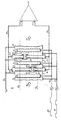
- The invention will now be described by way of example with reference to the accompanying drawing which is a top-view diagram of a charge coupled device embodying the invention. For the sake of clarity, the drawing is not necessarily to scale.
- The drawing shows two complete stages of an "N-channel" semiconductor charge coupled device in a split electrode
transversal filter configuration 10. More specifically, these stages includeshield gate electrodes 7, 11 and 15, first clock phase (P,) driven electrodes 5, 9, and 13, second clock phase (PJ drivenelectrodes - As known in the art, all electrodes are located in an oxide insulating layer on a major surface of a silicon semiconductor body. The electrodes are thus insulated from the underlying semiconductor surface by the oxide, and this oxide is thinner between electrode and semiconductor in the region between the dotted lines 28 and 29 than outside this region, in order to define the charge transfer channel for charge packet propagation in the left-to-right ("longitudinal") direction in the semiconductor between these dotted lines 28 and 29. All electrodes extend across the entire charge transfer channel, except for the gaps between segments of the split electrodes.
- The external connections to the
device 10 are as follows. A shieldelectrode metallization line 25 terminates in a terminal for application to all shield gate electrodes of a voltage bias source VSG, typically of about +8 volts for an "N-channel" device (electron charge carriers propagating in a P-type semiconductor charge transfer channel). A firstclack phase line 21 terminates in a first clock phase voltage source P for application to all the first clock phase electrodes of a first clock phasepulse voltage sequence 41, typically of about +5 volts passive phase and of about +13 volts active phase for an N-channel device. A secondclock phase line 22 terminates in a second clock phase voltage source P2 for application to all the second clock phase electrodes of a second clock phase pulse voltage sequence 42, typically of about +5 volts passive phase and + 17 volts active phase for an N-channel device. - The lower segments 8.1, 12.1 of each of the split electrodes are connected together by a first
sense electrode line 23 to a first sense electrode terminal 23.5, typically the negative input terminal of a differential sense amplifier. The upper segments 8.2, 12.2 of each of the split electrodes are connected together by a secondsense electrode line 24 to a second sense electrode terminal 24.5, typically the positive input terminal of the differential sense amplifier. Further details of a similar sense amplifier and its operation may be found, for example, in a paper by Y. P. Tsividis and P. R. Gray, published in IEEE Journal of Solid State Circuits, Vol. SC-11 (December 1976), pp. 748-753. It should be understood, however, that other known sensing techniques can be used for the purpose of detecting the output of the split electrode charge coupleddevice configuration 10. As is known, the relative lengths of the electrodes determine the frequency detected by the amplifier. - The shaded areas in the Figure represent impurity doped regions at the surface of the underlying semiconductor. More specifically, for an N-channei device, shaded regions 8.3 and 12.3 are N+ type conductivity surface connecting regions in the P-type semiconductor underlying the gaps between the split electrodes 8.1, 8.2 and 12.1, 12.2. These N+ connecting regions extend in the direction transverse to the charge packet transfer direction underneath the gap all the way from one segment to the other segment of each corresponding split electrode. In this way, each of these N+ connecting regions is of sufficient transverse extent to connect the two charge transfer sites underlying the two electrode segments of each split electrode pair, in order to provide a barrier-free equilibration path for the charge packets in the two transfer sites of each pair. With proper surface potential equilibration the contribution to output signal provided by each electrode is proportional to electrode length, as required for proper frequency selection.
- The shaded regions 8.4, 8.5 and 12.4, 12.5 are P+ conductivity surface barrier regions in the underlying semiconductor. Thus, there P+ regions are of the same conductivity type as that of the silicon substrate but are of much higher electrical conductivity. Also, ease of fabrication, using electrodes as masks, and to minimize the effects of misalignment, makes it advantageous that the longitudinal extent of each such barrier region be limited, on the side away from the N+ connecting region, by the outer contour of an electrode. Thus, for example, the left-hand edge of the second
clock phase electrode 10 delimits the right-hand edge of the P+ barrier region 8.4. This P+ barrier region 8.4 is contiguous along the entire downstream (right-hand) edge of the N+ connecting region 8.3. The purpose of this P+ region is to act as a barrier against a signal dependent injection of charges out of the N+ region 8.3 into the transfer site underneath first clock phase electrode 9 during operation. Thus, during operation, charges in the N+ connecting region 8.3 must overcome a constant potential barrier between the N+ region 8.3 and the transfer sites under the split electrode segments 8.1 and 8.2, obtained by the longer and circuitous path around the barrier region 8.4, which poses an even higher barrier, in order to enter the charge packet stream. Accordingly, in order for this path to indeed be relatively long, the P+ barrier region 8.4 advantageously extends at least about a distance in the direction transverse to the charge transfer propagation direction equal to the width of the gap between the electrode segments 8.1 and 8.2. The P+ barrier region 8.5 located on the upstream edge of the connecting region 8.3 is for purposes ot alignment and symmetry. For ease of fabrication, the barrier region 8.4 extends downstream only to the upstream edge of the secondclock phase electrode 10. It should be understood, of course, that the P+ barrier regions 12.4 and 12.5 are similar in relation to the N+ connecting region 12.3 as are the P+ barrier regions 8.4 and 8.5 in relation to the N+ connecting region 8.3. - Typically, the P-type silicon semiconductor material in the charge transfer channel contains an excess significant acceptor impurity concentration of the order of 7 x 10¹⁴ per cubic centimetre, the N+ connection regions contain an excess significant donor impurity concentration at the surface of the order of 2 x 10¹⁶ per cubic centimetre, and the P+ barrier regions contain an excess significant acceptor impurity concentration of the order of 2 x 10¹⁶ per cubic centimetre. Moreover, each P+ barrier region extends beyond the adjacent N+ connecting region, in the direction transverse to the charge transfer (or propagation) direction, for at least about a gap width on both edges of the N+ connecting region, in order to ensure a suitably geometrically complete barrier against the flow of charges out of the N+ connecting region. Thus, the transverse width of each P+ barrier region is at least about three times the width of the gap.
- In order to fabricate the device, a process including the following steps is illustrative. A first layer of silicon dioxide, typically about 50 nm thick, is grown all over a major surface of a P-type monocrystalline silicon semiconductor body. Then a layer of silicon nitride, typically about 120 nm thick, is formed on the entire exposed surface of the silicon dioxide, and a second layer of silicon dioxide, typically about 50 nm thick, is deposited over the entire exposed surface of the silicon nitride. Next, a photoresist layer, with apertures overlying those semiconductor regions where the P+ barrier regions are to be formed, is disposed over the exposed surface of the second silicon dioxide layer, and those portions of the second oxide layer in the apertures are selectively removed, as by etching. Acceptor impurities, such as boron, are then introduced through these apertures, to form the desired P+ barrier regions, as by ion implantation. The photoresist layer is then removed, and then those portions of the silicon nitride layer which are now exposed (i.e., in the apertures of the photoresist layer now removed) are removed, as by etching with a solution which dissolves silicon nitride but not the oxide. Next, an oxidation process in steam is used to grow silicon dioxide, typically 800 nm thick, over those regions where there is no nitride shielding the underlying silicon (i.e., in the complement of the removed photoresist layer). Thereby, the desired thick oxide, useful as a channel stop, is disposed in registry over the P+ barrier regions. Then an oxide etching solution is used for a sufficient time to dissolve slightly more than 50 nm of silicon dioxide, thereby removing completely the oxide layer overlying the silicon nitride but not removing the bulk of the 800 nm thick oxide, so that this latter oxide is still sufficiently thick to serve as a channel stop. Next the exposed silicon nitride is removed by an etching solution which does not dissolve the oxide, and then another slightly more than 50 nm of oxide are etched away by exposure to a solution which etches silicon dioxide, thereby exposing the silicon semiconductor surface in regions removed from the thick channel stop oxide (which still remains, being considerably more than 50 nm thick). Then a high quality gate oxide is thermally grown on the exposed silicon semiconductor surface. Next, polysilicon electrodes for the "first level of metallization" (electrodes 6, 8.1, 8.2, 10, 12.1, 12.2, 14) are laid down, as known in the art, with suitable gaps between the electrodes of every pair of split electrodes. Using these polysilicon electrodes as masks against diffusion, donor impurities, such as phosphorus, are introduced by ion implantation into the semiconductor in all the regions underlying these gaps; thereby the N+ connecting regions are formed. The outer edges of each connecting N+ region are determined in the CCD charge transfer direction by a boundary of the thick oxide, and thus by a boundary of each of the P+ barrier regions on both sides of each gap, while the outer edges of each of these N+ connecting regions in the transverse direction are determined by the extent of the gap between the corresponding split electrode, i.e. is self-aligned with the gap. Then the "second level metallization" (electrodes 5, 7, 9, 11, 13, 15) are formed of polysilicon, as known in the art, but with notches (as indicated in the drawing) in the neighbourhood of the split electrode gaps, in order to reduce the capacitance between these electrodes and the adjacent N+ connecting regions. These notches can be formed by suitable notches in the mask pattern used for the formation of these notched electrodes.
- Although the invention has been described in terms of a specific embodiment, various modifications may be made.
- For example, a P-channel CCD can be made by interchanging P with N, acceptor impurity with donor impurity, as known in the art. Also, the barrier regions can be provided solely by means of overlying thicker oxide regions or solely by means of the doped P+ regions rather than by both such means. Also, in some other fabrication techniques, it may be desirable that the P+ barrier regions be more highly doped than the N+ connecting regions, in order to ensure suitable channel stopping particularly in the absence of the use of a thick overlying channel stop oxide or to ensure proper mutual alignment of the boundary between the N+ connecting and P+ barrier regions. Finally, the invention is also applicable to bulk channel CCD split-electrode filters as well as the surface channel device described above in detail.
Claims (6)
Applications Claiming Priority (2)
| Application Number | Priority Date | Filing Date | Title |
|---|---|---|---|
| US05/818,411 US4126794A (en) | 1977-07-25 | 1977-07-25 | Semiconductor charge coupled device with split electrode configuration |
| US818411 | 1977-07-25 |
Publications (2)
| Publication Number | Publication Date |
|---|---|
| EP0000655A1 EP0000655A1 (en) | 1979-02-07 |
| EP0000655B1 true EP0000655B1 (en) | 1980-05-28 |
Family
ID=25225479
Family Applications (1)
| Application Number | Title | Priority Date | Filing Date |
|---|---|---|---|
| EP78300185A Expired EP0000655B1 (en) | 1977-07-25 | 1978-07-24 | Semiconductor charge coupled device with split electrode configuration |
Country Status (5)
| Country | Link |
|---|---|
| US (1) | US4126794A (en) |
| EP (1) | EP0000655B1 (en) |
| JP (1) | JPS5423482A (en) |
| DE (1) | DE2860017D1 (en) |
| IT (1) | IT1097398B (en) |
Families Citing this family (3)
| Publication number | Priority date | Publication date | Assignee | Title |
|---|---|---|---|---|
| FR2410908A1 (en) * | 1977-11-30 | 1979-06-29 | Thomson Csf | MULTIPLEX FILTERING DEVICE AND MODULATOR INCLUDING SUCH A DEVICE |
| US4348690A (en) * | 1981-04-30 | 1982-09-07 | Rca Corporation | Semiconductor imagers |
| JPS60178300A (en) * | 1984-02-23 | 1985-09-12 | 鹿島建設株式会社 | Method of construction of excavation of base rock |
Family Cites Families (4)
| Publication number | Priority date | Publication date | Assignee | Title |
|---|---|---|---|---|
| FR2302636A1 (en) * | 1975-02-28 | 1976-09-24 | Thomson Csf | ANALOGUE SIGNAL FILTERING PROCESS |
| US4005377A (en) * | 1975-09-02 | 1977-01-25 | General Electric Company | Conductivity coupled split capacitor signal processing device and apparatus therefor |
| JPS5277560A (en) * | 1975-12-24 | 1977-06-30 | Fujitsu Ltd | Transversal filter |
| US4075514A (en) * | 1976-12-06 | 1978-02-21 | Bell Telephone Laboratories, Incorporated | Sensing circuit for semiconductor charge transfer devices |
-
1977
- 1977-07-25 US US05/818,411 patent/US4126794A/en not_active Expired - Lifetime
-
1978
- 1978-07-21 JP JP8851478A patent/JPS5423482A/en active Granted
- 1978-07-24 EP EP78300185A patent/EP0000655B1/en not_active Expired
- 1978-07-24 DE DE7878300185T patent/DE2860017D1/en not_active Expired
- 1978-07-24 IT IT26032/78A patent/IT1097398B/en active
Also Published As
| Publication number | Publication date |
|---|---|
| DE2860017D1 (en) | 1980-10-16 |
| JPS5639060B2 (en) | 1981-09-10 |
| EP0000655A1 (en) | 1979-02-07 |
| JPS5423482A (en) | 1979-02-22 |
| IT1097398B (en) | 1985-08-31 |
| IT7826032A0 (en) | 1978-07-24 |
| US4126794A (en) | 1978-11-21 |
Similar Documents
| Publication | Publication Date | Title |
|---|---|---|
| US4314857A (en) | Method of making integrated CMOS and CTD by selective implantation | |
| US4825278A (en) | Radiation hardened semiconductor devices | |
| US3933529A (en) | Process for the production of a pair of complementary field effect transistors | |
| US4316203A (en) | Insulated gate field effect transistor | |
| US4319261A (en) | Self-aligned, field aiding double polysilicon CCD electrode structure | |
| US4910569A (en) | Charge-coupled device having improved transfer efficiency | |
| US4484209A (en) | SOS Mosfet with thinned channel contact region | |
| US4077111A (en) | Self-aligned gate field effect transistor and method for making same | |
| KR100211635B1 (en) | Semiconductor device and manufacturing method | |
| US4126794A (en) | Semiconductor charge coupled device with split electrode configuration | |
| US4725872A (en) | Fast channel single phase buried channel CCD | |
| US4142199A (en) | Bucket brigade device and process | |
| US4364164A (en) | Method of making a sloped insulator charge-coupled device | |
| US4099317A (en) | Method for fabricating self-aligned CCD devices and their output self-aligned MOS transistors on a single semiconductor substrate | |
| US5114833A (en) | Charge-coupled device and process of making the device | |
| JPS61198676A (en) | Semiconductor integrated circuit device | |
| US4906584A (en) | Fast channel single phase buried channel CCD | |
| JPH0352218B2 (en) | ||
| US4677737A (en) | Self aligned zero overlap charge coupled device | |
| US4358890A (en) | Process for making a dual implanted drain extension for bucket brigade device tetrode structure | |
| US4171229A (en) | Improved process to form bucket brigade device | |
| US4728622A (en) | Charge transfer device having a width changing channel | |
| JPH022644A (en) | Charge coupling device and its manufacture | |
| US4862235A (en) | Electrode structure for a corner turn in a series-parallel-series charge coupled device | |
| US6107124A (en) | Charge coupled device and method of fabricating the same |
Legal Events
| Date | Code | Title | Description |
|---|---|---|---|
| PUAI | Public reference made under article 153(3) epc to a published international application that has entered the european phase |
Free format text: ORIGINAL CODE: 0009012 |
|
| AK | Designated contracting states |
Designated state(s): BE DE FR GB NL SE |
|
| 17P | Request for examination filed | ||
| GRAA | (expected) grant |
Free format text: ORIGINAL CODE: 0009210 |
|
| AK | Designated contracting states |
Designated state(s): BE DE FR GB NL SE |
|
| REF | Corresponds to: |
Ref document number: 2860017 Country of ref document: DE Date of ref document: 19801016 |
|
| PGFP | Annual fee paid to national office [announced via postgrant information from national office to epo] |
Ref country code: DE Payment date: 19840625 Year of fee payment: 7 |
|
| PGFP | Annual fee paid to national office [announced via postgrant information from national office to epo] |
Ref country code: SE Payment date: 19840630 Year of fee payment: 7 Ref country code: BE Payment date: 19840630 Year of fee payment: 7 |
|
| PGFP | Annual fee paid to national office [announced via postgrant information from national office to epo] |
Ref country code: FR Payment date: 19840703 Year of fee payment: 7 |
|
| PG25 | Lapsed in a contracting state [announced via postgrant information from national office to epo] |
Ref country code: SE Effective date: 19860725 |
|
| PG25 | Lapsed in a contracting state [announced via postgrant information from national office to epo] |
Ref country code: BE Effective date: 19860731 |
|
| BERE | Be: lapsed |
Owner name: WESTERN ELECTRIC CY INC. Effective date: 19860731 |
|
| PG25 | Lapsed in a contracting state [announced via postgrant information from national office to epo] |
Ref country code: FR Free format text: LAPSE BECAUSE OF NON-PAYMENT OF DUE FEES Effective date: 19870331 |
|
| PG25 | Lapsed in a contracting state [announced via postgrant information from national office to epo] |
Ref country code: DE Effective date: 19870401 |
|
| GBPC | Gb: european patent ceased through non-payment of renewal fee | ||
| REG | Reference to a national code |
Ref country code: FR Ref legal event code: ST |
|
| PGFP | Annual fee paid to national office [announced via postgrant information from national office to epo] |
Ref country code: NL Payment date: 19870731 Year of fee payment: 10 |
|
| PG25 | Lapsed in a contracting state [announced via postgrant information from national office to epo] |
Ref country code: GB Effective date: 19881117 |
|
| PG25 | Lapsed in a contracting state [announced via postgrant information from national office to epo] |
Ref country code: NL Effective date: 19890201 |
|
| NLV4 | Nl: lapsed or anulled due to non-payment of the annual fee | ||
| EUG | Se: european patent has lapsed |
Ref document number: 78300185.2 Effective date: 19870518 |
|
| PLBE | No opposition filed within time limit |
Free format text: ORIGINAL CODE: 0009261 |
|
| STAA | Information on the status of an ep patent application or granted ep patent |
Free format text: STATUS: NO OPPOSITION FILED WITHIN TIME LIMIT |