DE202008018175U1 - Light-emitting semiconductor device - Google Patents
Light-emitting semiconductor device Download PDFInfo
- Publication number
- DE202008018175U1 DE202008018175U1 DE202008018175U DE202008018175U DE202008018175U1 DE 202008018175 U1 DE202008018175 U1 DE 202008018175U1 DE 202008018175 U DE202008018175 U DE 202008018175U DE 202008018175 U DE202008018175 U DE 202008018175U DE 202008018175 U1 DE202008018175 U1 DE 202008018175U1
- Authority
- DE
- Germany
- Prior art keywords
- light
- layer
- conductivity type
- semiconductor layer
- semiconductor device
- Prior art date
- Legal status (The legal status is an assumption and is not a legal conclusion. Google has not performed a legal analysis and makes no representation as to the accuracy of the status listed.)
- Expired - Lifetime
Links
Images

Classifications
-
- H—ELECTRICITY
- H01—ELECTRIC ELEMENTS
- H01L—SEMICONDUCTOR DEVICES NOT COVERED BY CLASS H10
- H01L33/00—Semiconductor devices with at least one potential-jump barrier or surface barrier specially adapted for light emission; Processes or apparatus specially adapted for the manufacture or treatment thereof or of parts thereof; Details thereof
- H01L33/02—Semiconductor devices with at least one potential-jump barrier or surface barrier specially adapted for light emission; Processes or apparatus specially adapted for the manufacture or treatment thereof or of parts thereof; Details thereof characterised by the semiconductor bodies
- H01L33/26—Materials of the light emitting region
- H01L33/30—Materials of the light emitting region containing only elements of group III and group V of the periodic system
- H01L33/32—Materials of the light emitting region containing only elements of group III and group V of the periodic system containing nitrogen
-
- H—ELECTRICITY
- H01—ELECTRIC ELEMENTS
- H01L—SEMICONDUCTOR DEVICES NOT COVERED BY CLASS H10
- H01L33/00—Semiconductor devices with at least one potential-jump barrier or surface barrier specially adapted for light emission; Processes or apparatus specially adapted for the manufacture or treatment thereof or of parts thereof; Details thereof
- H01L33/005—Processes
- H01L33/0093—Wafer bonding; Removal of the growth substrate
-
- H—ELECTRICITY
- H01—ELECTRIC ELEMENTS
- H01L—SEMICONDUCTOR DEVICES NOT COVERED BY CLASS H10
- H01L33/00—Semiconductor devices with at least one potential-jump barrier or surface barrier specially adapted for light emission; Processes or apparatus specially adapted for the manufacture or treatment thereof or of parts thereof; Details thereof
- H01L33/36—Semiconductor devices with at least one potential-jump barrier or surface barrier specially adapted for light emission; Processes or apparatus specially adapted for the manufacture or treatment thereof or of parts thereof; Details thereof characterised by the electrodes
- H01L33/40—Materials therefor
- H01L33/405—Reflective materials
-
- H—ELECTRICITY
- H01—ELECTRIC ELEMENTS
- H01L—SEMICONDUCTOR DEVICES NOT COVERED BY CLASS H10
- H01L33/00—Semiconductor devices with at least one potential-jump barrier or surface barrier specially adapted for light emission; Processes or apparatus specially adapted for the manufacture or treatment thereof or of parts thereof; Details thereof
- H01L33/44—Semiconductor devices with at least one potential-jump barrier or surface barrier specially adapted for light emission; Processes or apparatus specially adapted for the manufacture or treatment thereof or of parts thereof; Details thereof characterised by the coatings, e.g. passivation layer or anti-reflective coating
Abstract
Lichtemittierende Halbleitervorrichtung (100), umfassend: eine lichtemittierende Struktur (105), umfassend eine Halbleiterschicht (102) des ersten Leitungstyps, eine Halbleiterschicht (104) des zweiten Leitungstyps und eine aktive Schicht (103) zwischen der Halbleiterschicht (102) des ersten Leitungstyps und der Halbleiterschicht (104) des zweiten Leitungstyps, und eine erste Elektrode (112) auf der Halbleiterschicht (102) des ersten Leitungstyps, wobei die lichtemittierende Struktur (105) eine äußere Nut (106) umfasst, die auf einem äußeren Bereich der lichtemittierenden Struktur (105) derart ausgebildet ist, dass die Dicke des äußeren Bereichs der lichtemittierenden Struktur (105) kleiner als die Dicke eines inneren Bereichs der lichtemittierenden Struktur (105) ist.A semiconductor light emitting device (100) comprising: a light emitting structure (105) comprising a semiconductor layer (102) of the first conductivity type, a semiconductor layer (104) of the second conductivity type and an active layer (103) between the semiconductor layer (102) of the first conductivity type and the semiconductor layer (104) of the second conductivity type, and a first electrode (112) on the semiconductor layer (102) of the first conductivity type, the light-emitting structure (105) comprising an outer groove (106) which is formed on an outer region of the light-emitting structure ( 105) is designed such that the thickness of the outer region of the light-emitting structure (105) is smaller than the thickness of an inner region of the light-emitting structure (105).
Description
Technisches GebietTechnical area
Die vorliegende Offenbarung betrifft eine lichtemittierende Halbleitervorrichtung.The present disclosure relates to a semiconductor light-emitting device.
Technischer HintergrundTechnical background
III–V-Gruppen-Nitridhalbleiter sind vielfältig für optische Vorrichtungen, wie zum Beispiel blaue/grüne LEDs (Leuchtdioden), Hochgeschwindigkeitsschaltelemente, wie zum Beispiel MOSFET (Metallhalbleiterfeldeffekttransistor) und HEMT (Heteroübergangsfeldeffekttransistor; Transistor mit hoher Elektronenbeweglichkeit), eine Lichtquelle für eine Beleuchtungs- oder Anzeigevorrichtung u. d. gl. verwendet worden. Insbesondere hat eine lichtemittierende Vorrichtung, die einen Gruppe-III-Nitridhalbleiter verwendet, eine direkte Übergangsbandlücke, die dem Bereich sichtbarer Strahlung oder ultravioletter Strahlung entspricht und hocheffizient Licht emittieren kann.III-V group nitride semiconductors are versatile for optical devices such as blue / green LEDs, high speed switching elements such as MOSFET (metal semiconductor field effect transistor) and HEMT (heterojunction field effect transistor), a light source for illumination. or display device u. d. gl. has been used. In particular, a light-emitting device using a group III nitride semiconductor has a direct junction bandgap which corresponds to the range of visible radiation or ultraviolet radiation and can emit light highly efficiently.
Der Nitridhalbleiter wurde hauptsächlich als LED oder als LD (Laserdiode) verwendet und Forschung zum Verbessern des Herstellungsverfahrens oder der Lichteffizienz wurde durchgeführt.The nitride semiconductor has been mainly used as an LED or an LD (laser diode), and research for improving the manufacturing process or the light efficiency has been made.
Offenbarung der ErfindungDisclosure of the invention
Technisches ProblemTechnical problem
Ausführungsbeispiele sehen eine lichtemittierende Halbleitervorrichtung vor, bei welchen jede Schicht mit einer lichtemittierenden Struktur räumlich isolierbar ist.Embodiments provide a semiconductor light-emitting device in which each layer having a light-emitting structure is spatially isolable.
Ausführungsbeispiele sehen eine lichtemittierende Halbleitervorrichtung vor, umfassend eine äußere Schutzschicht am äußeren Umfang zwischen einer lichtemittierenden Struktur und einem leitenden Stützsubstrat und auch das Entfernen des äußeren Umfangs der lichtemittierenden Struktur.Embodiments provide a semiconductor light emitting device comprising an outer protective layer on the outer periphery between a light emitting structure and a conductive supporting substrate and also removing the outer periphery of the light emitting structure.
Technische LösungTechnical solution
Ein Ausführungsbeispiel sieht eine lichtemittierende Halbleitervorrichtung vor, umfassend: Eine lichtemittierende Struktur, umfassend eine Halbleiterschicht eines ersten Leitungstyps, eine aktive Schicht unter der Halbleiterschicht des ersten Leitungstyps und eine Halbleiterschicht eines zweiten Leitungstyps unter der aktiven Schicht, eine reflektierende Elektrodenschicht unter der lichtemittierenden Struktur, und eine äußere Schutzschicht an einem äußeren Umfang der reflektierenden Elektrodenschicht.One embodiment provides a semiconductor light emitting device comprising: a light emitting structure comprising a first conductivity type semiconductor layer, an active layer below the first conductivity type semiconductor layer and a second conductivity type semiconductor layer below the active layer, a reflective electrode layer below the light emitting structure, and an outer protective layer on an outer circumference of the reflective electrode layer.
Ein Ausführungsbeispiel sieht eine lichtemittierende Halbleitervorrichtung vor, umfassend: Eine lichtemittierende Struktur, umfassend eine Halbleiterschicht eines ersten Leitungstyps, eine aktive Schicht unter der Halbleiterschicht des ersten Leitungstyps, eine Halbleiterschicht eines zweiten Halbleitertyps unter der aktiven Schicht und eine äußere Nut an einem äußeren Umfang einer jeder der Schichten und eine reflektierende Elektrodenschicht unter der lichtemittierenden Struktur.An embodiment provides a semiconductor light emitting device comprising: a light emitting structure comprising a first conductivity type semiconductor layer, an active layer under the first conductivity type semiconductor layer, a second type semiconductive semiconductor layer under the active layer, and an outer periphery at each outer periphery thereof of the layers and a reflective electrode layer under the light-emitting structure.
Vorteilhafte EffekteAdvantageous effects
Gemäß den Ausführungsbeispielen können, falls Material, wie zum Beispiel dielektrisches Material nicht am Außenbereich der lichtemittierenden Struktur ausgebildet ist, durch Kontaktieren bzw. Aufbringen von dielektrischem Material am Außenbereich der lichtemittierenden Struktur verursachte Spannungen vermindert werden.According to the embodiments, if material such as dielectric material is not formed on the outer portion of the light-emitting structure, voltages caused by contacting dielectric material on the outer portion of the light-emitting structure can be reduced.
Gemäß den Ausführungsbeispielen kann, falls dielektrisches Material nicht am Außenbereich der lichtemittierenden Struktur ausgebildet ist, das Herstellungsverfahren der lichtemittierenden Vorrichtung verbessert werden.According to the embodiments, if dielectric material is not formed on the outer portion of the light-emitting structure, the manufacturing method of the light-emitting device can be improved.
Gemäß den Ausführungsbeispielen kann die Zuverlässigkeit der lichtemittierenden Vorrichtung verbessert werden.According to the embodiments, the reliability of the light-emitting device can be improved.
Kurze Beschreibung der ZeichnungenBrief description of the drawings
Beste Ausführungsform zum Ausführen der ErfindungBest embodiment for carrying out the invention
Nachfolgend wird eine lichtemittierende Halbleitervorrichtung und ein Verfahren zum Herstellen derselben gemäß den Ausführungsbeispielen genau unter Bezugnahme zu den beiliegenden Zeichnungen beschrieben. In der vorliegenden Beschreibung wird, wenn eine Schicht (oder ein Film) als auf/unter einer anderen Schicht bezogen wird, die Beschreibung mit Bezug zu den beiliegenden Zeichnungen ausgeführt. Die Dicke einer jeden Schicht kann als ein Beispiel beschrieben sein und ist nicht auf die Dicke der Ausführungsbeispiele gemäß den beiliegenden Zeichnungen beschränkt.Hereinafter, a semiconductor light-emitting device and a method of manufacturing the same according to the embodiments will be described in detail with reference to the accompanying drawings. In the present specification, when a layer (or a film) is referred to as being on / under another layer, the description will be made with reference to the accompanying drawings. The thickness of each layer may be described as an example and is not limited to the thickness of the embodiments shown in the accompanying drawings.
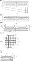
Gemäß
Die Halbleiterschicht
Die aktive Schicht
Die Halbleiterschicht
Eine Struktur aus der Halbleiterschicht
Eine transparente Schicht (nicht dargestellt) kann unter der Halbleiterschicht
Zusätzlich ist eine Schicht der lichtemittierenden Halbleitervorrichtung
Zusätzlich ist die reflektierende Elektrodenschicht
Die erste Elektrode
Zusätzlich ist die äußere Schutzschicht
Die äußere Schutzschicht
Die äußere Schutzschicht
Der Außenbereich der Halbleiterschicht
Weiterhin kann, da ein zusätzliches dielektrisches Material nicht auf der äußeren Nut
Gemäß diesem Ausführungsbeispiel kann, weil die äußere Nut
Die äußere Schutzschicht
Die Tiefe der äußeren Nut
Darüber hinaus ist die Breite W2 der äußeren Nut
Die
Gemäß den
Hier wächst die dünne Nitridschicht auf dem Wafersubstrat
Das Wafersubstrat
Gemäß
Die aktive Schicht
Eine Halbleiterschicht
Eine Struktur der Halbleiterschicht
In der lichtemittierenden Halbleitervorrichtung
Gemäß der
Eine äußere Schutzschicht
Falls die äußere Schutzschicht
In einem Chip ist die Breite W1 der äußeren Schutzschicht
Wenn einmal die äußere Schutzschicht
Gemäß
Gemäß
Gemäß den
Hier wird, wenn eine Pufferschicht oder/und eine undotierte Halbleiterschicht (nicht dargestellt) zwischen dem Wafersubstrat
Ein Polierverfahren kann mittels eines induktiv gekoppelten Plasma/Reaktiven Ionenätzen (IZP/RCE) auf der Unterseite der Halbleiterschicht
Gemäß
Eine äußere Nut
Die äußere Nut
Gemäß
Gemäß
Es versteht sich, dass in der Beschreibung, wenn eine Schicht (oder Film) als auf oder unter einer anderen Schicht bezogen wird, sie direkt oder indirekt auf oder unter der anderen Schicht sein kann.It should be understood that in the description, when a layer (or film) is referred to as being on or under another layer, it may be directly or indirectly on or below the other layer.
Jeder Bezug in dieser Beschreibung zu einem Ausführungsbeispiel, eine Ausführungsform, ein Ausführungsbeispiel, etc., bedeutet, dass ein bestimmtes Merkmal, Struktur oder Eigenschaft in Verbindung mit der Ausführungsform beschrieben wird, welches in zumindest einer Ausführungsform der vorliegenden Erfindung enthalten ist. Das Erscheinen von solchen Ausdrücken an unterschiedlichen Stellen in der Beschreibung bedeutet nicht notwendigerweise, dass sich alle auf das gleiche Ausführungsbeispiel beziehen. Weiterhin, wenn ein bestimmtes Merkmal, eine Struktur oder eine Eigenschaft in Verbindung mit einem Ausführungsbeispiel beschrieben wird, wird es innerhalb des Bereichs eines Fachmannes unterstellt, dass ein solches Merkmal, Struktur oder Eigenschaft auf andere der Ausführungsbeispiele übertragen werden kann.Any reference in this specification to an embodiment, an embodiment, an embodiment, etc., means that a particular feature, structure, or characteristic will be described in connection with the embodiment included in at least one embodiment of the present invention. The appearance of such terms in different places throughout the specification does not necessarily mean that all refer to the same embodiment. Furthermore, when describing a particular feature, structure, or characteristic in connection with one embodiment, it will be understood, within the scope of one of ordinary skill in the art, that such feature, structure or feature may be applied to other of the embodiments.
Obwohl Ausführungsbeispiele mit Bezug zu einer Anzahl von erläuternden Ausführungsbeispielen davon beschrieben worden sind, sollte verstanden werden, dass zahlreiche andere Modifikationen und Ausführungsformen, die von einem Fachmann abgeleitet werden können, in den Umfang und den Bereich der Prinzipien der vorliegenden Offenbarung fallen. Insbesondere sind unterschiedliche Abwandlungen und Modifikationen der Komponententeile und/oder Anordnungen der gegenständlichen Kombinationsanordnungen innerhalb des Umfangs der Offenbarung, der Zeichnung und der beigefügten Ansprüche möglich. Zusätzlich zu den Variationen und Modifikationen an den Komponententeilen und/oder Anordnungen können alternative Verwendungen für Fachleute augenscheinlich sein.Although embodiments have been described with reference to a number of illustrative embodiments thereof, it should be understood that numerous other modifications and embodiments that may be in the art of one of skill fall within the scope and scope of the principles of the present disclosure. In particular, various modifications and variations of the component parts and / or arrangements of the subject combination arrangements within the scope of the disclosure, the drawings and the appended claims are possible. In addition to the variations and modifications to the component parts and / or arrangements, alternative uses for those skilled in the art may be apparent.
Industrielle AnwendbarkeitIndustrial applicability
Gemäß den Ausführungsbeispielen, wenn das Material, wie zum Beispiel dielektrisches Material, nicht am Außenbereich der lichtemittierenden Struktur ausgebildet wird, kann durch die Berührung mit dem dielektrischen Material am Außenbereich der lichtemittierenden Struktur verursachte Spannung reduziert werden.According to the embodiments, when the material such as dielectric material is not formed on the outer portion of the light-emitting structure, stress caused by contact with the dielectric material at the outer portion of the light-emitting structure can be reduced.
Gemäß den Ausführungsbeispielen kann, falls das dielektrische Material nicht auf dem Außenbereich der lichtemittierenden Struktur ausgebildet ist, das Herstellungsverfahren der lichtemittierenden Vorrichtung verbessert werden.According to the embodiments, if the dielectric material is not formed on the outer portion of the light-emitting structure, the manufacturing method of the light-emitting device can be improved.
Gemäß den Ausführungsbeispielen kann die Zuverlässigkeit der lichtemittierenden Vorrichtung verbessert werden.According to the embodiments, the reliability of the light-emitting device can be improved.
Claims (15)
Applications Claiming Priority (2)
| Application Number | Priority Date | Filing Date | Title |
|---|---|---|---|
| KR20070061429 | 2007-06-22 | ||
| KR1020070061429A KR100872717B1 (en) | 2007-06-22 | 2007-06-22 | Light emitting device and manufacturing method thereof |
Publications (1)
| Publication Number | Publication Date |
|---|---|
| DE202008018175U1 true DE202008018175U1 (en) | 2011-12-08 |
Family
ID=40186144
Family Applications (1)
| Application Number | Title | Priority Date | Filing Date |
|---|---|---|---|
| DE202008018175U Expired - Lifetime DE202008018175U1 (en) | 2007-06-22 | 2008-06-18 | Light-emitting semiconductor device |
Country Status (7)
| Country | Link |
|---|---|
| US (3) | US7989820B2 (en) |
| EP (2) | EP2816614B1 (en) |
| JP (1) | JP5450399B2 (en) |
| KR (1) | KR100872717B1 (en) |
| CN (2) | CN101681959B (en) |
| DE (1) | DE202008018175U1 (en) |
| WO (1) | WO2009002040A2 (en) |
Families Citing this family (37)
| Publication number | Priority date | Publication date | Assignee | Title |
|---|---|---|---|---|
| DE102007029370A1 (en) * | 2007-05-04 | 2008-11-06 | Osram Opto Semiconductors Gmbh | Semiconductor chip and method for producing a semiconductor chip |
| KR100872717B1 (en) * | 2007-06-22 | 2008-12-05 | 엘지이노텍 주식회사 | Light emitting device and manufacturing method thereof |
| KR101534848B1 (en) | 2008-07-21 | 2015-07-27 | 엘지이노텍 주식회사 | Light emitting diode and method for fabricating the light emitting diode, and light emitting device and method for fabricating light emitting devcie |
| KR100999793B1 (en) | 2009-02-17 | 2010-12-08 | 엘지이노텍 주식회사 | Fabrication method for semiconductor light emitting device |
| US20100327300A1 (en) * | 2009-06-25 | 2010-12-30 | Koninklijke Philips Electronics N.V. | Contact for a semiconductor light emitting device |
| JP2011035017A (en) * | 2009-07-30 | 2011-02-17 | Hitachi Cable Ltd | Light-emitting device |
| KR101072034B1 (en) | 2009-10-15 | 2011-10-10 | 엘지이노텍 주식회사 | Semiconductor light emitting device and fabrication method thereof |
| KR101081193B1 (en) * | 2009-10-15 | 2011-11-07 | 엘지이노텍 주식회사 | Semiconductor light emitting device and fabrication method thereof |
| KR101014013B1 (en) | 2009-10-15 | 2011-02-10 | 엘지이노텍 주식회사 | Semiconductor light emitting device and fabrication method thereof |
| KR20110062128A (en) * | 2009-12-02 | 2011-06-10 | 엘지이노텍 주식회사 | Light emitting device, light emitting device package and method for fabricating the same |
| EP2942823B1 (en) | 2009-12-09 | 2021-05-05 | LG Innotek Co., Ltd. | Light emitting device, light emitting package, and lighting system |
| KR100999701B1 (en) | 2010-02-03 | 2010-12-08 | 엘지이노텍 주식회사 | Light emitting device, method for fabricating the light emitting device and light emitting device package |
| KR100986374B1 (en) * | 2009-12-09 | 2010-10-08 | 엘지이노텍 주식회사 | Light emitting device, method for fabricating the light emitting device and light emitting device package |
| KR100986353B1 (en) * | 2009-12-09 | 2010-10-08 | 엘지이노텍 주식회사 | Light emitting device, method for fabricating the light emitting device and light emitting device package |
| KR101039904B1 (en) * | 2010-01-15 | 2011-06-09 | 엘지이노텍 주식회사 | Light emitting device, light emitting device package and method for fabricating the same |
| KR100999779B1 (en) * | 2010-02-01 | 2010-12-08 | 엘지이노텍 주식회사 | Light emitting device, method for fabricating the same and light emitting device package |
| KR100986523B1 (en) | 2010-02-08 | 2010-10-07 | 엘지이노텍 주식회사 | Semiconductor light emitting device and fabrication method thereof |
| KR100986318B1 (en) | 2010-02-09 | 2010-10-08 | 엘지이노텍 주식회사 | Semiconductor light emitting device and fabrication method thereof |
| KR100999798B1 (en) * | 2010-02-11 | 2010-12-08 | 엘지이노텍 주식회사 | Semiconductor light emitting device and fabrication method thereof |
| KR100969100B1 (en) * | 2010-02-12 | 2010-07-09 | 엘지이노텍 주식회사 | Light emitting device, method for fabricating the same and light emitting device package |
| KR101020995B1 (en) * | 2010-02-18 | 2011-03-09 | 엘지이노텍 주식회사 | Light emitting device, method of fabricating the light emitting device and light emitting device package |
| KR100999692B1 (en) * | 2010-02-18 | 2010-12-08 | 엘지이노텍 주식회사 | Light emitting device, method for fabricating the light emitting device and light emitting device package |
| US8338317B2 (en) | 2011-04-06 | 2012-12-25 | Infineon Technologies Ag | Method for processing a semiconductor wafer or die, and particle deposition device |
| KR101028277B1 (en) | 2010-05-25 | 2011-04-11 | 엘지이노텍 주식회사 | Light emitting device, method for fabricating the light emitting device, light emitting device package and lighting unit |
| KR101182920B1 (en) * | 2010-07-05 | 2012-09-13 | 엘지이노텍 주식회사 | Light emitting device and fabrication method thereof |
| KR101000311B1 (en) * | 2010-07-27 | 2010-12-13 | (주)더리즈 | Semiconductor light emitting device and manufacturing method of the same |
| DE102010045784B4 (en) * | 2010-09-17 | 2022-01-20 | OSRAM Opto Semiconductors Gesellschaft mit beschränkter Haftung | Optoelectronic semiconductor chip |
| CN103733359A (en) * | 2011-08-09 | 2014-04-16 | 三星电子株式会社 | Method for manufacturing a semiconductor light-emitting element and semiconductor light-emitting element manufactured thereby |
| JP5992695B2 (en) * | 2012-02-29 | 2016-09-14 | スタンレー電気株式会社 | Semiconductor light emitting element array and vehicle lamp |
| CN103489965A (en) * | 2012-06-13 | 2014-01-01 | 联胜光电股份有限公司 | Light emitting diode with reflector protective layer |
| JP5440674B1 (en) * | 2012-09-18 | 2014-03-12 | ウシオ電機株式会社 | LED element and manufacturing method thereof |
| JP6068091B2 (en) * | 2012-10-24 | 2017-01-25 | スタンレー電気株式会社 | Light emitting element |
| JP5818031B2 (en) * | 2013-03-21 | 2015-11-18 | ウシオ電機株式会社 | LED element |
| CN103594594B (en) * | 2013-11-08 | 2016-09-07 | 溧阳市江大技术转移中心有限公司 | There is the inverted light-emitting diode (LED) of roughening transparency electrode |
| JP2015191976A (en) * | 2014-03-27 | 2015-11-02 | ウシオ電機株式会社 | Semiconductor light emitting element and manufacturing method of the same |
| CN113540283B (en) * | 2021-06-18 | 2023-01-24 | 西安理工大学 | Two-dimensional electron gas type photoconductive longitudinal switch and manufacturing method thereof |
| CN114336268B (en) * | 2022-03-04 | 2022-05-31 | 苏州长光华芯光电技术股份有限公司 | High-reliability low-defect semiconductor light-emitting device and preparation method thereof |
Family Cites Families (32)
| Publication number | Priority date | Publication date | Assignee | Title |
|---|---|---|---|---|
| JP2953468B2 (en) | 1989-06-21 | 1999-09-27 | 三菱化学株式会社 | Compound semiconductor device and surface treatment method thereof |
| US5358880A (en) * | 1993-04-12 | 1994-10-25 | Motorola, Inc. | Method of manufacturing closed cavity LED |
| JP3241976B2 (en) * | 1995-10-16 | 2001-12-25 | 株式会社東芝 | Semiconductor light emitting device |
| JPH114042A (en) | 1997-06-10 | 1999-01-06 | Nippon Telegr & Teleph Corp <Ntt> | Semiconductor laser and manufacture thereof |
| JP2000114666A (en) * | 1998-10-09 | 2000-04-21 | Sanyo Electric Co Ltd | Semiconductor light emitting element and manufacturing method |
| JP3469484B2 (en) | 1998-12-24 | 2003-11-25 | 株式会社東芝 | Semiconductor light emitting device and method of manufacturing the same |
| JP2001223384A (en) * | 2000-02-08 | 2001-08-17 | Toshiba Corp | Semiconductor light-emitting element |
| JP4024994B2 (en) * | 2000-06-30 | 2007-12-19 | 株式会社東芝 | Semiconductor light emitting device |
| US20020017652A1 (en) | 2000-08-08 | 2002-02-14 | Stefan Illek | Semiconductor chip for optoelectronics |
| US6555405B2 (en) | 2001-03-22 | 2003-04-29 | Uni Light Technology, Inc. | Method for forming a semiconductor device having a metal substrate |
| US7057211B2 (en) * | 2001-10-26 | 2006-06-06 | Ammono Sp. Zo.O | Nitride semiconductor laser device and manufacturing method thereof |
| TWI278995B (en) * | 2002-01-28 | 2007-04-11 | Nichia Corp | Nitride semiconductor element with a supporting substrate and a method for producing a nitride semiconductor element |
| CN101694871B (en) * | 2002-11-11 | 2012-12-05 | 株式会社半导体能源研究所 | Process for fabricating light emitting device |
| US6831309B2 (en) * | 2002-12-18 | 2004-12-14 | Agilent Technologies, Inc. | Unipolar photodiode having a schottky junction contact |
| US6806112B1 (en) * | 2003-09-22 | 2004-10-19 | National Chung-Hsing University | High brightness light emitting diode |
| JP2005191530A (en) * | 2003-12-03 | 2005-07-14 | Sumitomo Electric Ind Ltd | Light emitting device |
| DE102004021175B4 (en) | 2004-04-30 | 2023-06-29 | OSRAM Opto Semiconductors Gesellschaft mit beschränkter Haftung | Semiconductor chips for optoelectronics and methods for their manufacture |
| KR100513923B1 (en) | 2004-08-13 | 2005-09-08 | 재단법인서울대학교산학협력재단 | Growth method of nitride semiconductor layer and light emitting device using the growth method |
| JP2006073619A (en) | 2004-08-31 | 2006-03-16 | Sharp Corp | Nitride based compound semiconductor light emitting diode |
| CN100409461C (en) * | 2004-10-20 | 2008-08-06 | 晶元光电股份有限公司 | Structure of LED and its mfg method |
| JP2006228855A (en) * | 2005-02-16 | 2006-08-31 | Rohm Co Ltd | Semiconductor light emitting element and manufacturing method thereof |
| JP2006253298A (en) | 2005-03-09 | 2006-09-21 | Toshiba Corp | Semiconductor light emitting element and device therefor |
| US20060237735A1 (en) | 2005-04-22 | 2006-10-26 | Jean-Yves Naulin | High-efficiency light extraction structures and methods for solid-state lighting |
| KR100638819B1 (en) * | 2005-05-19 | 2006-10-27 | 삼성전기주식회사 | Vertical nitride based semiconductor light emitting device having improved light extraction efficiency |
| JP2007158131A (en) * | 2005-12-06 | 2007-06-21 | Toyoda Gosei Co Ltd | Group iii nitride-based compound semiconductor optical element |
| JP2007080896A (en) * | 2005-09-12 | 2007-03-29 | Sanyo Electric Co Ltd | Semiconductor element |
| JP2007157853A (en) | 2005-12-01 | 2007-06-21 | Sony Corp | Semiconductor light-emitting element, and method of manufacturing same |
| DE102006061167A1 (en) * | 2006-04-25 | 2007-12-20 | Osram Opto Semiconductors Gmbh | Optoelectronic semiconductor component |
| JP4946195B2 (en) * | 2006-06-19 | 2012-06-06 | サンケン電気株式会社 | Semiconductor light emitting device and manufacturing method thereof |
| JP4302720B2 (en) | 2006-06-28 | 2009-07-29 | 株式会社沖データ | Semiconductor device, LED head, and image forming apparatus |
| US7915624B2 (en) | 2006-08-06 | 2011-03-29 | Lightwave Photonics, Inc. | III-nitride light-emitting devices with one or more resonance reflectors and reflective engineered growth templates for such devices, and methods |
| KR100872717B1 (en) * | 2007-06-22 | 2008-12-05 | 엘지이노텍 주식회사 | Light emitting device and manufacturing method thereof |
-
2007
- 2007-06-22 KR KR1020070061429A patent/KR100872717B1/en active IP Right Review Request
-
2008
- 2008-06-18 DE DE202008018175U patent/DE202008018175U1/en not_active Expired - Lifetime
- 2008-06-18 WO PCT/KR2008/003437 patent/WO2009002040A2/en active Application Filing
- 2008-06-18 CN CN2008800151926A patent/CN101681959B/en active Active
- 2008-06-18 EP EP14178650.9A patent/EP2816614B1/en active Active
- 2008-06-18 CN CN201310054919.4A patent/CN103151439B/en active Active
- 2008-06-18 US US12/516,956 patent/US7989820B2/en not_active Expired - Fee Related
- 2008-06-18 EP EP08766398.5A patent/EP2160772B1/en active Active
- 2008-06-18 JP JP2010513109A patent/JP5450399B2/en active Active
-
2011
- 2011-06-28 US US13/171,139 patent/US8994053B2/en active Active
-
2013
- 2013-01-18 US US13/745,402 patent/US8664682B2/en active Active
Also Published As
| Publication number | Publication date |
|---|---|
| JP5450399B2 (en) | 2014-03-26 |
| CN103151439B (en) | 2016-06-22 |
| WO2009002040A3 (en) | 2009-02-26 |
| EP2160772A2 (en) | 2010-03-10 |
| US7989820B2 (en) | 2011-08-02 |
| US8664682B2 (en) | 2014-03-04 |
| US20100065872A1 (en) | 2010-03-18 |
| CN101681959A (en) | 2010-03-24 |
| KR100872717B1 (en) | 2008-12-05 |
| EP2816614B1 (en) | 2022-05-04 |
| EP2160772B1 (en) | 2014-09-03 |
| US20130126899A1 (en) | 2013-05-23 |
| JP2010531058A (en) | 2010-09-16 |
| US8994053B2 (en) | 2015-03-31 |
| EP2816614A1 (en) | 2014-12-24 |
| EP2160772A4 (en) | 2011-11-16 |
| CN103151439A (en) | 2013-06-12 |
| US20110254041A1 (en) | 2011-10-20 |
| WO2009002040A2 (en) | 2008-12-31 |
| CN101681959B (en) | 2013-03-27 |
Similar Documents
| Publication | Publication Date | Title |
|---|---|---|
| DE202008018175U1 (en) | Light-emitting semiconductor device | |
| DE202009018431U1 (en) | Semiconductor light Emmi animal-end device | |
| DE19725578B4 (en) | Reduction of crack formation in the material of III-V nitride semiconductor components while maximizing the electrical doping | |
| DE202010017388U1 (en) | Light-emitting semiconductor device | |
| DE202009018441U1 (en) | Light-emitting semiconductor device | |
| DE102018101658A1 (en) | Light-emitting device | |
| DE102005053274A1 (en) | Making semiconductor chips involves building up semiconductor layers, applying metal plating to epitaxial growth substrate and depositing metal layer galvanically before structuring and separating layers into individual chips | |
| DE10000088A1 (en) | Indium aluminum gallium nitride light-emitting device such as surface or edge emitting laser comprises host substrate, light-emitting structure, device contacts and wafer bonding layer between substrate and light-emitting structure | |
| KR101707118B1 (en) | Light emitting diode and method for fabricating the light emitting device | |
| KR102303502B1 (en) | Light emitting device and light emitting device package having thereof | |
| US8859315B2 (en) | Epitaxial wafer and manufacturing method thereof | |
| KR20160102774A (en) | Light emitting device and light unit having thereof | |
| DE112017003572T5 (en) | ULTRAVIOLETTE LIGHT-EMITTING DIODE | |
| US20100163903A1 (en) | Semiconductor light emitting device | |
| DE102004050891B4 (en) | Light-emitting III-nitride semiconductor device | |
| KR101749154B1 (en) | light-emitting diode chip and manufacturing method thereof | |
| DE10203809B4 (en) | Radiation-emitting semiconductor component | |
| KR101845611B1 (en) | High Efficiency Light Emitting Diode Having Optical Functionalized Electrodes | |
| CN101840969A (en) | Semiconductor photoelectric element capable of improving light removal rate and manufacturing method thereof | |
| DE102016116704A1 (en) | Light-emitting device and method for its production | |
| DE102018118824A1 (en) | SEMICONDUCTOR COMPONENT WITH A STRESS COMPENSATION LAYER AND METHOD FOR PRODUCING A SEMICONDUCTOR COMPONENT | |
| WO2020165029A1 (en) | Optoelectronic semiconductor component having sections of a conductive layer and method for producing an optoelectronic semiconductor component | |
| TW202046515A (en) | Infrared led device | |
| KR102489464B1 (en) | Light emitting device and method of fabricating the same | |
| WO2019002097A1 (en) | Semiconductor chip with transparent current spreading layer |
Legal Events
| Date | Code | Title | Description |
|---|---|---|---|
| R207 | Utility model specification |
Effective date: 20120202 |
|
| R150 | Utility model maintained after payment of first maintenance fee after three years | ||
| R150 | Utility model maintained after payment of first maintenance fee after three years |
Effective date: 20120306 |
|
| R151 | Utility model maintained after payment of second maintenance fee after six years |
Effective date: 20140522 |
|
| R152 | Utility model maintained after payment of third maintenance fee after eight years | ||
| R071 | Expiry of right |