DE10241301A1 - Electrooptic light control element and display and medium for television and computer screens has temperature driven control mechanism - Google Patents
Electrooptic light control element and display and medium for television and computer screens has temperature driven control mechanism Download PDFInfo
- Publication number
- DE10241301A1 DE10241301A1 DE10241301A DE10241301A DE10241301A1 DE 10241301 A1 DE10241301 A1 DE 10241301A1 DE 10241301 A DE10241301 A DE 10241301A DE 10241301 A DE10241301 A DE 10241301A DE 10241301 A1 DE10241301 A1 DE 10241301A1
- Authority
- DE
- Germany
- Prior art keywords
- electrodes
- layers
- layer
- light control
- electro
- Prior art date
- Legal status (The legal status is an assumption and is not a legal conclusion. Google has not performed a legal analysis and makes no representation as to the accuracy of the status listed.)
- Withdrawn
Links
Classifications
-
- G—PHYSICS
- G02—OPTICS
- G02F—OPTICAL DEVICES OR ARRANGEMENTS FOR THE CONTROL OF LIGHT BY MODIFICATION OF THE OPTICAL PROPERTIES OF THE MEDIA OF THE ELEMENTS INVOLVED THEREIN; NON-LINEAR OPTICS; FREQUENCY-CHANGING OF LIGHT; OPTICAL LOGIC ELEMENTS; OPTICAL ANALOGUE/DIGITAL CONVERTERS
- G02F1/00—Devices or arrangements for the control of the intensity, colour, phase, polarisation or direction of light arriving from an independent light source, e.g. switching, gating or modulating; Non-linear optics
- G02F1/01—Devices or arrangements for the control of the intensity, colour, phase, polarisation or direction of light arriving from an independent light source, e.g. switching, gating or modulating; Non-linear optics for the control of the intensity, phase, polarisation or colour
- G02F1/13—Devices or arrangements for the control of the intensity, colour, phase, polarisation or direction of light arriving from an independent light source, e.g. switching, gating or modulating; Non-linear optics for the control of the intensity, phase, polarisation or colour based on liquid crystals, e.g. single liquid crystal display cells
- G02F1/137—Devices or arrangements for the control of the intensity, colour, phase, polarisation or direction of light arriving from an independent light source, e.g. switching, gating or modulating; Non-linear optics for the control of the intensity, phase, polarisation or colour based on liquid crystals, e.g. single liquid crystal display cells characterised by the electro-optical or magneto-optical effect, e.g. field-induced phase transition, orientation effect, guest-host interaction or dynamic scattering
- G02F1/139—Devices or arrangements for the control of the intensity, colour, phase, polarisation or direction of light arriving from an independent light source, e.g. switching, gating or modulating; Non-linear optics for the control of the intensity, phase, polarisation or colour based on liquid crystals, e.g. single liquid crystal display cells characterised by the electro-optical or magneto-optical effect, e.g. field-induced phase transition, orientation effect, guest-host interaction or dynamic scattering based on orientation effects in which the liquid crystal remains transparent
- G02F1/1393—Devices or arrangements for the control of the intensity, colour, phase, polarisation or direction of light arriving from an independent light source, e.g. switching, gating or modulating; Non-linear optics for the control of the intensity, phase, polarisation or colour based on liquid crystals, e.g. single liquid crystal display cells characterised by the electro-optical or magneto-optical effect, e.g. field-induced phase transition, orientation effect, guest-host interaction or dynamic scattering based on orientation effects in which the liquid crystal remains transparent the birefringence of the liquid crystal being electrically controlled, e.g. ECB-, DAP-, HAN-, PI-LC cells
-
- G—PHYSICS
- G02—OPTICS
- G02F—OPTICAL DEVICES OR ARRANGEMENTS FOR THE CONTROL OF LIGHT BY MODIFICATION OF THE OPTICAL PROPERTIES OF THE MEDIA OF THE ELEMENTS INVOLVED THEREIN; NON-LINEAR OPTICS; FREQUENCY-CHANGING OF LIGHT; OPTICAL LOGIC ELEMENTS; OPTICAL ANALOGUE/DIGITAL CONVERTERS
- G02F1/00—Devices or arrangements for the control of the intensity, colour, phase, polarisation or direction of light arriving from an independent light source, e.g. switching, gating or modulating; Non-linear optics
- G02F1/01—Devices or arrangements for the control of the intensity, colour, phase, polarisation or direction of light arriving from an independent light source, e.g. switching, gating or modulating; Non-linear optics for the control of the intensity, phase, polarisation or colour
- G02F1/07—Devices or arrangements for the control of the intensity, colour, phase, polarisation or direction of light arriving from an independent light source, e.g. switching, gating or modulating; Non-linear optics for the control of the intensity, phase, polarisation or colour based on electro-optical liquids exhibiting Kerr effect
-
- G—PHYSICS
- G02—OPTICS
- G02F—OPTICAL DEVICES OR ARRANGEMENTS FOR THE CONTROL OF LIGHT BY MODIFICATION OF THE OPTICAL PROPERTIES OF THE MEDIA OF THE ELEMENTS INVOLVED THEREIN; NON-LINEAR OPTICS; FREQUENCY-CHANGING OF LIGHT; OPTICAL LOGIC ELEMENTS; OPTICAL ANALOGUE/DIGITAL CONVERTERS
- G02F1/00—Devices or arrangements for the control of the intensity, colour, phase, polarisation or direction of light arriving from an independent light source, e.g. switching, gating or modulating; Non-linear optics
- G02F1/01—Devices or arrangements for the control of the intensity, colour, phase, polarisation or direction of light arriving from an independent light source, e.g. switching, gating or modulating; Non-linear optics for the control of the intensity, phase, polarisation or colour
- G02F1/13—Devices or arrangements for the control of the intensity, colour, phase, polarisation or direction of light arriving from an independent light source, e.g. switching, gating or modulating; Non-linear optics for the control of the intensity, phase, polarisation or colour based on liquid crystals, e.g. single liquid crystal display cells
- G02F1/133—Constructional arrangements; Operation of liquid crystal cells; Circuit arrangements
- G02F1/1333—Constructional arrangements; Manufacturing methods
- G02F1/1343—Electrodes
- G02F1/134309—Electrodes characterised by their geometrical arrangement
- G02F1/134363—Electrodes characterised by their geometrical arrangement for applying an electric field parallel to the substrate, i.e. in-plane switching [IPS]
-
- G—PHYSICS
- G02—OPTICS
- G02F—OPTICAL DEVICES OR ARRANGEMENTS FOR THE CONTROL OF LIGHT BY MODIFICATION OF THE OPTICAL PROPERTIES OF THE MEDIA OF THE ELEMENTS INVOLVED THEREIN; NON-LINEAR OPTICS; FREQUENCY-CHANGING OF LIGHT; OPTICAL LOGIC ELEMENTS; OPTICAL ANALOGUE/DIGITAL CONVERTERS
- G02F1/00—Devices or arrangements for the control of the intensity, colour, phase, polarisation or direction of light arriving from an independent light source, e.g. switching, gating or modulating; Non-linear optics
- G02F1/01—Devices or arrangements for the control of the intensity, colour, phase, polarisation or direction of light arriving from an independent light source, e.g. switching, gating or modulating; Non-linear optics for the control of the intensity, phase, polarisation or colour
- G02F1/13—Devices or arrangements for the control of the intensity, colour, phase, polarisation or direction of light arriving from an independent light source, e.g. switching, gating or modulating; Non-linear optics for the control of the intensity, phase, polarisation or colour based on liquid crystals, e.g. single liquid crystal display cells
- G02F1/133—Constructional arrangements; Operation of liquid crystal cells; Circuit arrangements
- G02F1/1333—Constructional arrangements; Manufacturing methods
- G02F1/133382—Heating or cooling of liquid crystal cells other than for activation, e.g. circuits or arrangements for temperature control, stabilisation or uniform distribution over the cell
-
- G—PHYSICS
- G02—OPTICS
- G02F—OPTICAL DEVICES OR ARRANGEMENTS FOR THE CONTROL OF LIGHT BY MODIFICATION OF THE OPTICAL PROPERTIES OF THE MEDIA OF THE ELEMENTS INVOLVED THEREIN; NON-LINEAR OPTICS; FREQUENCY-CHANGING OF LIGHT; OPTICAL LOGIC ELEMENTS; OPTICAL ANALOGUE/DIGITAL CONVERTERS
- G02F1/00—Devices or arrangements for the control of the intensity, colour, phase, polarisation or direction of light arriving from an independent light source, e.g. switching, gating or modulating; Non-linear optics
- G02F1/01—Devices or arrangements for the control of the intensity, colour, phase, polarisation or direction of light arriving from an independent light source, e.g. switching, gating or modulating; Non-linear optics for the control of the intensity, phase, polarisation or colour
- G02F1/13—Devices or arrangements for the control of the intensity, colour, phase, polarisation or direction of light arriving from an independent light source, e.g. switching, gating or modulating; Non-linear optics for the control of the intensity, phase, polarisation or colour based on liquid crystals, e.g. single liquid crystal display cells
- G02F1/137—Devices or arrangements for the control of the intensity, colour, phase, polarisation or direction of light arriving from an independent light source, e.g. switching, gating or modulating; Non-linear optics for the control of the intensity, phase, polarisation or colour based on liquid crystals, e.g. single liquid crystal display cells characterised by the electro-optical or magneto-optical effect, e.g. field-induced phase transition, orientation effect, guest-host interaction or dynamic scattering
- G02F1/13793—Blue phases
Abstract
Description
Gebiet der ErfindungField of the Invention
Die vorliegende Erfindung betrifft
Lichtsteuerelemente sowie diese enthaltende Anzeigen. Die Lichtsteuerelemente
verwenden bevorzugt Steuermedien die bei bestimmten Temperaturen
anisotrope Eigenschaften aufweisen, wie z. B: Flüssigkristalle. Die Lichtsteuerelemente
werden bei einer Temperatur betrieben, bei der die Steuermedien
in der isotropen Phase vorliegen. Derartige Anzeigen sind in der
bislang unveröffentlichten
Patentanmeldung
Die vorliegende Erfindung betrifft ein elektrooptisches Lichtsteuerelement sowie solche Elemente enthaltende elektrooptische Anzeigen und Anzeigesysteme wie beispielsweise Fernsehbildschirme und Computermonitore. Die erfindungsgemäßen Lichtsteuerelemente enthalten ein mesogenes Steuermedium, das beim Betrieb der Lichtsteuerelemente in der isotropen Phase vorliegt. Sie sind neben einem guten Kontrast und einer geringen Blickwinkelabhängigkeit des Kontrasts besonders durch sehr kurze Schaltzeiten ausgezeichnet.The present invention relates to an electro-optical light control element and containing such elements electro-optical displays and display systems such as television screens and computer monitors. The light control elements according to the invention contain a mesogenic control medium that is used when operating the light control elements is in the isotropic phase. They are next to a good contrast and a low dependence of the contrast on the viewing angle characterized by very short switching times.
Ferner betrifft die vorliegende Erfindung Medien und deren Verwendung als Steuermedien in derartigen Lichtsteuerelementen.The present invention further relates to Media and their use as control media in such light control elements.
Aufgabe und Stand der TechnikTask and State of the art
Konventionelle elektrooptischen Flüssigkristallanzeigen
sind allgemein bekannt. Sie werden bei einer Temperatur betrieben,
bei der sich das Steuermedium in einer Mesophase, bei den meisten
Anzeigetypen in der nematischen Phase, befindet. In der Mesophase
haben die Steuermedien bereits anisotrope Eigenschaften, wie zum
Beispiel eine Doppelbrechung (Δn).
Diese wird nicht erst durch ein elektrisches Feld induziert. Am
weitesten verbreitet sind TN-(Englisch: "twisted nematic") und STN- (Englisch: "super
twisted nematic") Anzeigen. Die Flüssigkristallzellen dieser Anzeigen
haben Elektroden auf den Substraten auf den beiden einander gegenüberliegenden
Seiten des Flüssigkristallmediums.
Somit ist das elektrische Feld im wesentlichen vertikal zur Flüssigkristallschicht.
Insbesondere die zuerst genannten Anzeigen werden in Kombination
mit einer TFT (Englisch: thin film transistor) Ansteuerung für Anzeigen
mit großem
Informationsgehalt und großer Auflösung verwendet.
So zum Beispiel in "lap-top" und "note-book" Computern. Insbesondere
bei "desktop" Computermonitoren werden in neuerer Zeit zunehmend
Flüssigkristallanzeigen
des IPS-(Englisch: in-plane switching, z. B.
Allen diesen konventionellen Anzeigen ist ein relativ langsames Schalten gemein, insbesondere ist dieses für die immer stärkere Verbreitung findenden TV- und Multi-Media-Anwendungen nicht ausreichend. Dieses fällt insbesondere im Vergleich mit den nahezu ubiquitären Kathodenstrahlröhren auf. Ein weiterer Nachteil der bekannten, in Flüssigkristallanzeigen eingesetzten elektro-optischen Effekte ist die deutliche Blickwinkelabhängigkeit des erzielten Kontrasts. Diese ist in den meisten Fällen so groß, daß für Anzeigen im Direktsichtbetrieb Kompensationsschichten, typischerweise anisotrope Filme, mit zum Teil kompliziertem Aufbau, verwendet werden müssen.All of these conventional displays a relatively slow shift is common, in particular this is for the always stronger Widespread TV and multimedia applications are not sufficient. This falls in particular compared to the almost ubiquitous cathode ray tubes. Another disadvantage of the known ones used in liquid crystal displays electro-optical effects is the clear viewing angle dependency of the contrast achieved. This is the case in most cases large, that for ads in direct vision mode compensation layers, typically anisotropic Films, some with a complicated structure, must be used.
In der unveröffentlichten Anmeldung
Diese Lichtsteuerelemente schalten besonders schnell und haben eine gute Blickwinkelabhängigkeit des Kontrasts. Allerdings sind die Ansteuerspannungen für viele Anwendungen zu hoch.Switch these light controls particularly fast and have a good viewing angle dependence of the Contrast. However, the drive voltages are for many Applications too high.
Die in der noch nicht offengelegten
Anmeldung
Der vorliegenden Erfindung lag die Aufgabe zugrunde besonders schnell schaltende Lichtsteuerelemente mit guter Blickwinkelabhängigkeit und insbesondere mit niedrigen Ansteuerspannungen zu realisieren. Diese Lichtsteuerelemente sollen eine möglichst geringe Schichtdicke der Steuermedien aufweisen um als Elemente von FPDs (Englisch: flat panel displays, also flachen Anzeigen), wie zum Beispiel Flachbildschirmen für Computer, eingesetzt werden zu können. Ferner sollen sie mittels einer möglichst einfachen Elektrodenkonfiguration ansteuerbar sein und eine niedrige Betriebsspannung aufweisen. Darüber hinaus sollen sie für die Anwendung in elektrooptischen Anzeigen einen guten Kontrast mit einer geringen Blickwinkelabhängigkeit haben.The present invention was based on the object of realizing particularly quickly switching light control elements with good viewing angle dependency and in particular with low control voltages. These light control elements should have the smallest possible layer thickness of the control media in order to Elements of FPDs (English: flat panel displays), such as flat screens for computers, can be used. Furthermore, they should be controllable using the simplest possible electrode configuration and have a low operating voltage. In addition, they should have a good contrast with a low viewing angle dependence for use in electro-optical displays.
Somit besteht der Bedarf nach verbesserten Lichtsteuerelementen insbesondere mit verringerter Ansteuerspannung.Thus there is a need for improved ones Light control elements in particular with a reduced control voltage.
Vorliegende ErfindungThis invention
Überraschend
wurde gefunden, dass, wie im Folgenden beschrieben, Lichtsteuerelemente
die in der unveröffentlichten
Anmeldung
Die elektrooptischen Lichtsteuerelemente gemäß der vorliegenden Erfindung umfassen
- – ein Substrat oder mehrere Substrate,
- – eine Elektrodenanordnung,
- – mindestens ein Element oder mehrere Elemente zur Polarisation des Lichts und
- – ein
Steuermedium,
und sind dadurch gekkennzeichnet, dass
- – das Lichtsteuerelement bei einer Temperatur betrieben wird, bei der das Steuermedium im nicht angesteuerten Zustand in der isotropen Phase vorliegt und dass
- – die Elektrodenanordnung ein elektrisches Feld mit einer signifikanten Komponente parallel zur Fläche des mesogenen Steuermediums erzeugen kann und dass
- – die Elektrodenanordnung so gestaltet ist, dass mindestens eine eine der vier folgenden Bedingungen erfüllt ist
- – die in der Ebene der Steuerschicht einander benachbarten elektrisch leitfähigen Schichten haben einen Abstand von 10 μm oder weniger voneinander,
- – die leitfähige Schicht oder, wenn mehrere der elektrisch der leitfähigen Schichten vorhanden sind, eine oder mehrere dieser Schichten der Elektrodenstruktur ist bzw. sind erhaben,
- – die Elektrodenstruktur umfaßt jeweils zwei oder mehrere Schichten die einander überlagern, elektrisch leitend miteinander verbunden sind und gleichzeitig über wesentliche Teile ihrer Fläche voneinander durch eine dielektrische Schicht getrennt sind,
- – die elektrisch leitfähige Schicht oder, wenn mehrere der elektrisch der leitfähigen Schichten vorhanden sind, eine oder mehrere der leitfähigen Schichten der Elektrodenstruktur ist bzw. sind durch eine feste dielektrische Schicht vom jeweiligen darunterliegenden Substrat getrennt.
- One or more substrates,
- An electrode arrangement,
- - At least one or more elements for polarizing the light and
- - a control medium, and are characterized in that
- - The light control element is operated at a temperature at which the control medium is in the non-activated state in the isotropic phase and that
- - The electrode arrangement can generate an electric field with a significant component parallel to the surface of the mesogenic control medium and that
- - The electrode arrangement is designed so that at least one of the four following conditions is met
- The electrically conductive layers which are adjacent to one another in the plane of the control layer are at a distance of 10 μm or less from one another,
- The conductive layer or, if several of the electrically conductive layers are present, one or more of these layers of the electrode structure is or are raised,
- The electrode structure in each case comprises two or more layers which overlap one another, are electrically conductively connected to one another and at the same time are separated from one another by a dielectric layer over substantial parts of their area,
- - The electrically conductive layer or, if several of the electrically conductive layers are present, one or more of the conductive layers of the electrode structure is or are separated from the respective underlying substrate by a solid dielectric layer.
Neben der niedrigen Ansteuerspannung ist insbesondere der Kontrast dieser Anzeigen und seine Blickwinkelabhängigkeit hervorragend und die Schaltzeiten sind sehr kurz. In addition to the low control voltage is in particular the contrast of these displays and its viewing angle dependency excellent and the switching times are very short.
Im Folgenden wird die vorliegende Erfindung näher erläutert.The following is the present Invention closer explained.
Bevorzugt wird als Steuermedium des Lichtsteuerelements ein mesogenes Medium verwendet. Als mesogene Medien werden in der vorliegenden Anmeldung Medien bezeichnet, die eine Mesophase aufweisen, die in einer Mesophase löslich sind oder eine Mesophase induzieren. Die Mesophase ist eine smektische oder eine nematische Phase, bevorzugt eine nematische Phase.Is preferred as the control medium Light control element uses a mesogenic medium. As a mesogenic Media are referred to in the present application as media that have a mesophase that is soluble in a mesophase or induce a mesophase. The mesophase is a smectic or a nematic phase, preferably a nematic phase.
Als bevorzugtes Medium zur Untersuchung der mesogenen Eigenschaften der Medien die keine Mesophase aufweisen wird die nematische Mischung ZLI-4792 der Merck KGaA, Darmstadt, Deutschland verwendet. Bevorzugt haben die mesogenen Medien einen aus 10%-iger Lösung in dieser Mischung extrapolierten Klärpunkt von –100°C oder mehr, besonders bevorzugt von –50°C oder mehr und ganz besonders bevorzugt von –20°C oder mehr.As the preferred medium for investigation the mesogenic properties of the media that have no mesophase the nematic mixture ZLI-4792 from Merck KGaA, Darmstadt, Germany used. The mesogenic media preferably have one from a 10% solution in this mixture extrapolated clearing point of -100 ° C or more, particularly preferred of –50 ° C or more and most preferably from -20 ° C or more.
Die erfindungsgemäßen Lichtsteuerelemente enthalten bevorzugt ein mesogenes Medium, das bei Betriebstemperatur in der isotropen Phase vorliegt. Dieses Medium befindet sich zweckmäßiger Weise auf bzw. unter einem Substrat.The light control elements according to the invention contain preferably a mesogenic medium, which at the operating temperature in the isotropic phase. This medium is convenient on or under a substrate.
In der Regel befindet sich das Steuermedium zwischen zwei Substraten. Diese Ausführungsform ist bevorzugt. Wenn sich das Steuermedium zwischen zwei Substraten befindet ist mindestens eines dieser Substrate lichtdurchlässig. Das lichtdurchlässige Substrat, bzw. die lichtdurchlässigen Substrate können z. B. aus Glas, Quarz oder Kunststoff bestehen. Wird ein Substrat verwendet, das nicht lichtdurchlässig ist, so kann dies unter anderem aus einem Metall oder einem Halbleiter bestehen. Diese Medien können als solche verwendet werden oder auf einem Träger, z.B. einer Keramik, vorliegen. Ist das Steuermedium ein polymeres Medium so kann gegebenenfalls auf die Verwendung eines zweiten Substrats verzichtet werden. Polymere Steuermedium können sogar selbsttragend ausgeführt werden. In diesem Fall wird gar kein Substrat benötigt.The control medium is usually located between two substrates. This embodiment is preferred. If the control medium is between two substrates, at least one of these substrates is translucent. The translucent substrate, or the translucent substrates can, for. B. consist of glass, quartz or plastic. If a substrate is used that is not translucent, this can consist, among other things, of a metal or a semiconductor. These media can be used as such or can be present on a carrier, for example a ceramic. If the control medium is a polymeric medium, the use of a second substrate can optionally be dispensed with. Polymer control medium can even be self-supporting. In this case, no substrate is required.
Die Betriebstemperatur des Lichtsteuerelements liegt bevorzugt oberhalb der Übergangstemperatur des Steuermediums zur isotropen Phase, in der Regel im Bereich von 0,1° bis 50° oberhalb dieser Übergangstemperatur, bevorzugt im Bereich von 0,1° bis 10° oberhalb dieser Übergangstemperatur und besonders bevorzugt im Bereich von 0,1° bis 5° oberhalb dieser Übergangstemperatur.The operating temperature of the light control element is preferably above the transition temperature of the Control medium for the isotropic phase, usually in the range from 0.1 ° to 50 ° above this transition temperature, preferably in the range from 0.1 ° to 10 ° above this transition temperature and particularly preferably in the range from 0.1 ° to 5 ° above this transition temperature.
Bei Anlegen einer Spannung wird in dem mesogenen Medium in der isotropen Phase eine Orientierung induziert welche zu einer optischen Verzögerung führt, die auf bekannte Weise visualisiert werden kann. Bevorzugt wird ein inhomogenes elektrisches Feld angewendet.When a voltage is applied in orientation is induced in the mesogenic medium in the isotropic phase which leads to an optical delay leads, which can be visualized in a known manner. Is preferred applied an inhomogeneous electric field.
Die erfindungsgemäßen Lichtsteuerelemente enthalten mindestens ein Element zur Polarisierung des Lichts. Zusätzlich enthalten sie bevorzugt ein weiteres optisches Element. Dieses weitere optische Element ist entweder ein zweites Element zur Polarisaton des Lichts, ein Reflektor oder ein Transflektor.The light control elements according to the invention contain at least one element for polarizing light. Also included it prefers another optical element. This further optical Element is either a second element to polarize light, a reflector or a transflector.
Die optischen Elemente sind so angeordnet, dass das Licht beim Durchgang durch das mesogene Medium des Lichtsteuerelements sowohl vor dem Eintritt in das mesogene Medium, als auch nach dem Austritt aus dem mesogenen Medium mindestens einmal mindestens ein polarisierendes Element durchläuft.The optical elements are arranged that the light as it passes through the mesogenic medium of the light control element both before entering the mesogenic medium and after Leaving the mesogenic medium at least once at least passes through polarizing element.
In einer bevorzugten Ausführungsform des Lichtsteuerelements gemäß der vorliegenden Erfindung befindet sich das mesogene Medium zwischen zwei Polarisatoren, also einem Polarisator und einem Analysator. Bevorzugt werden zwei Linearpalarisatoren verwendet. In dieser Ausführungsform sind die Absorptionsachsen der Polarisatoren bevorzugt gekreuzt und bilden bevorzugt einen Winkel von 90°.In a preferred embodiment of the light control element according to the present Invention, the mesogenic medium is between two polarizers, so a polarizer and an analyzer. Two are preferred Linear palaisators used. In this embodiment, the absorption axes are the polarizers are preferably crossed and preferably form one 90 ° angle.
Optional enthält das erfindungsgemäße Lichtsteuerelement eine oder mehrere doppelbrechende Schichten. Bevorzugt enthält es eine λ/4-Schicht oder mehrere λ/4-Schichten, bevorzugt eine λ/4-Schicht. Die optische Verzögerung der λ/4-Schicht beträgt bevorzugt ca. 140 nm.The light control element according to the invention optionally contains one or more birefringent layers. It preferably contains one λ / 4 layer or several λ / 4 layers, preferably a λ / 4 layer. The optical delay the λ / 4 layer is preferably about 140 nm.
Die Schichtdicke (d) des mesogenen Steuermediums beträgt bevorzugt 0,1 μm bis 5.000 μm (i.e. 5 mm), besonders bevorzugt 0,5 μm bis 1.000 μm (i.e. 1 mm), besonders bevorzugt 1,0 μm bis 100 μm und ganz besonders bevorzugt 3,0 μm bis 30 μm und insbesondere 3,5 μm bis 20 μm. In einer bevorzugten Ausführungsform beträgt die Schichtdicke des mesogenen Steuermediums bevorzugt 0,5 μm bis 50 μm, besonders bevorzugt 1,0 μm bis 20 μm und ganz besonders bevorzugt 1,0 μm bis 8,0 μm.The layer thickness (d) of the mesogenic Control medium is preferably 0.1 μm up to 5,000 μm (i.e. 5 mm), particularly preferably 0.5 μm to 1,000 μm (i.e. 1 mm), particularly preferred 1.0 μm to 100 μm and very particularly preferably 3.0 μm up to 30 μm and in particular 3.5 μm up to 20 μm. In a preferred embodiment is the layer thickness of the mesogenic control medium is preferably 0.5 μm to 50 μm, particularly preferably 1.0 μm up to 20 μm and most preferably 1.0 μm up to 8.0 μm.
Gegenstand der vorliegenden Erfindung sind auch elektrooptische Anzeigen, die ein oder mehrere erfindungsgemäße Lichtsteuerelemente enthalten. Bevorzugt werden diese elektrooptischen Anzeigen mittels einer aktiven Matrix angesteuert.Object of the present invention are also electro-optical displays, the one or more light control elements according to the invention contain. These electro-optical displays are preferred by means of a active matrix.
Gegenstand der varliegenden Erfindung sind des weiteren elektrooptische Anzeigesysteme enthaftend eine oder mehrere erfindungsgemäße elektrooptische Anzeigen. Diese elektrooptische Anzeigesysteme werden bevorzugt zur Darstellung von Information, unter anderem, bevorzugt als Fernsehbildschirm oder als Computermonitor verwendet. Bei der darzustellenden Information handelt es sich bevorzugt um digitale Signale oder um Videosignale.The subject of the invention are also electro-optical display systems containing one or more electro-optical according to the invention Show. These electro-optical display systems are preferred to display information, among other things, preferably as a television screen or used as a computer monitor. With the information to be displayed it is preferably digital signals or video signals.
Das erfindungsgemäße Lichtsteuerelement kann zusätzlich ein oder mehrere weitere übliche optische Elemente wie doppelbrechende Schichten (z.B. Kompensationsschichten), Diffusorschichten, und Elemente zur Erhöhung der Helligkeit und/oder der Lichtausbeute und/oder der Blickwinkeiabhängigkeit enthalten, wobei diese Aufzählung nicht abschließend ist.The light control element according to the invention can additionally one or more other common ones optical elements such as birefringent layers (e.g. compensation layers), Diffuser layers, and elements to increase brightness and / or contain the luminous efficacy and / or the viewing angle dependency, these enumeration not concluding is.
Die erfindungsgemäßen Lichtsteuerelemente sind durch einen guten Kontrast gekennzeichnet, der stark und nahezu überwiegend von den Eigenschaften der verwendeten Polarisatoren abhängt. Zum Vergleich mit herkömmlichen TN-Zellen werden hier TN-Zellen mit einer optischen Verzögerung von 0,50 μm, positivem Kontrast und der Absorptionsachse der Polarisatoren senkrecht zu der Vorzugsorientierung der nematischen Flüssigkristalle am benachbarten Substrat, die nicht chirale Flüssigkristalle enthalten, herangezogen. Werden bei den erfindungsgemäßen Lichtsteuerelementen und bei diesen herkömmlichen TN-Zellen die gleichen Polarisatoren verwendet, ist der Kontrast der erfindungsgemäßen Lichtsteuerelemente um 40% oder mehr größer als der der TN-Zellen.The light control elements according to the invention are characterized by a good contrast that is strong and almost predominant depends on the properties of the polarizers used. To the Comparison with conventional ones TN cells become TN cells with an optical delay of 0.50 μm, positive contrast and the absorption axis of the polarizers perpendicular on the preferred orientation of the nematic liquid crystals on the neighboring one Substrate that is not chiral liquid crystals included. Are in the light control elements of the invention and with these conventional ones TN cells using the same polarizers is the contrast the light control elements according to the invention by 40% or more than that of TN cells.
Die Blickwinkelabhängigkeit des Kontrasts der erfindungsgemäßen Lichtsteuerelemente ist sehr gut. Sie ist deutlich besser als die der bekannten ECB-Zellen. Sie ist eher vergleichbar mit der bei den kommerziell verfügbaren IPS-Anzeigen (z.B. von Hitachi und NEC, beide Japan) und MVA-Anzeigen (z.B. von Fujitsu, Japan) beobachteten Blickwinkelabhängigkeit. Sie ist viel geringer als die der konventionellen TN-Anzeigen. So schließt eine Isokontrastkurve eines gegebenen Kontrastverhältnisses bei den erfindungsgemäßen Lichtsteuerelementen in der Regel einen Winkelbereich ein, die mehr als doppelt so groß, oft sogar mehr als dreimal so groß ist wie die entsprechende Isokontrastkurve für das gleiche Kontrastverhältnis bei der TN-Anzeige.The viewing angle dependency the contrast of the light control elements according to the invention is very good. It is significantly better than that of the known ECB cells. It is more comparable to that of the commercially available IPS advertisements (e.g. from Hitachi and NEC, both Japan) and MVA ads (e.g. from Fujitsu, Japan) observed viewing angle dependency. It is much less than that of conventional TN displays. So one closes Isocontrast curve of a given contrast ratio in the light control elements according to the invention usually an angular range that is more than twice as large, often even is more than three times the size like the corresponding isocontrast curve for the same contrast ratio the TN display.
Die Schaltzeiten der erfindungsgemäßen Lichtsteuerelemente sind sehr klein. Sie liegen in der Regel bei Werten von 1 ms oder weniger, bevorzugt bei 0,5 ms oder weniger besonders bevorzugt bei 0,1 ms oder weniger.The switching times of the light control elements according to the invention are very small. They are usually 1 ms or less less, preferably at 0.5 ms or less, particularly preferably at 0.1 ms or less.
Besonders vorteilhaft ist die Tatsache , dass beim Schalten zwischen verschiedenen Graustufen sowohl die Schaltzeit für das Ausschalten, als auch, besonders überraschend, die für das Einschalten nahezu unabhängig von der verwendeten Ansteuerspannung sind. Dies stellt einen wesentliche Vorteil gegenüber herkömmlichen Lichtsteuerelementen wie Flüssigkristallzellen, z.B. TN-Zellen, dar.The fact is particularly advantageous that when switching between different grayscale both the Switching time for turning it off, as well, particularly surprisingly, for turning it on almost independent of the control voltage used. This represents an essential one advantage over usual Light control elements such as liquid crystal cells, e.g. TN cells.
Zur Untersuchung des Schaltverhaltens bei der Ansteuerung von Graustufen wurden die erfindungsgemäßen Lichtsteuerelemente jeweils verschiedenen Ansteuerspannungen geschaltet. Dabei wurden charakteristische Spannungen der elektrooptischen Kennlinie als Endpunkte gewählt, z.B. V10, V2 0, V3 0,... bis V9 0. Dann wurde von einer gegebenen charakteristischen Spannung auf die anderen Spannungen und zurück geschaltet, z.B. von V10 auf jede der Spannungen V90, V80, V70 bis V2 0. Als nächstes wurde eine andere der charakteristischen Spannungen gewählt und von dieser auf jeder der höheren charakteristischen Spannungen und zurück geschaltet, z.B. von V20 auf jede der Spannungen V9 0, V80, V70 bis V30 und so weiter bis zur Ausgangsspannung V80 von der auf V9 0 und zurück geschaltet wird. Bei den Lichtsteuerelementen gemäß der vorliegenden Erfindung ist in allen diesen Fällen die Einschaltzeit vom Zeitpunkt des Einschaltens der neuen Spannung bis zum Erreichen von 90% der jeweiligen maximalen Transmissionsänderung für alle diese Schaltvorgänge in erster Näherung identisch.To investigate the switching behavior in the control of gray levels, the light control elements according to the invention were each switched to different control voltages. Characteristic voltages of the electro-optical characteristic were chosen as end points, for example V 10 , V 2 0 , V 3 0 , ... to V 9 0 . Then there was a switch from a given characteristic voltage to the other voltages and back, for example from V 10 to each of the voltages V 90 , V 80 , V 70 to V 2 0 . Another one of the characteristic voltages is selected next and on each of the higher characteristic voltages and switched back by this, for example, from V 20 on each of the voltages V 9 0, V 80, V 70 to V 30, and so on until the output voltage V 80 from which is switched to V 9 0 and back. In the case of the light control elements according to the present invention, the switch-on time from the point in time at which the new voltage is switched on until 90% of the respective maximum transmission change has been reached is identical for all of these switching processes in a first approximation.
Elektrooptische Anzeigen gemäß der vorliegenden Erfindung enthalten ein oder mehrere erfindungsgemäße Lichtsteuerelemente. Diese werden in einer bevorzugten Ausführungsform mittels einer Aktiven Matrix angesteuert.Electro-optical displays according to the present Invention contain one or more light control elements according to the invention. In a preferred embodiment, these are activated Matrix driven.
In einer anderen bevorzugten Ausführungsform werden die erfindungsgemäßen Lichtsteuerelemente im sogenannten „field sequential mode" angesteuert. Hierbei werden die Schaltelemente synchron zur Ansteuerung nacheinander mit verschieden farbigem Licht beleuchtet. Zur Erzeugung des gepulsten farbigen Lichts können beispielsweise ein Farbrad („color wheel"), Stroboskoplampen oder Blitzlampen eingesetzt. werden.In another preferred embodiment the light control elements according to the invention in so-called "field sequential mode ". The switching elements synchronized with the control one after the other with different colored light illuminated. To generate the pulsed colored light, for example a color wheel ("color wheel "), strobe lamps or flash lamps.
Elektrooptische Anzeigen gemäß der vorliegenden Erfindung können, insbesondere wenn sie für Fernsehbildschirme, Computermonitore oder ähnliches verwendet werden, zur Darstellung farbiger Bilder einen Farbfilter enthalten. Dieser Farbfilter besteht zweckmäßiger Weise aus einem Mosaik von Filterelementen verschiedener Farben. Hierbei ist typischer Weise jedem elektro-optischen Schaltelement ein Element des Farbfiltermosaiks einer Farbe zugeordnet.Electro-optical displays according to the present Invention can especially if they're for TV screens, Computer monitors or the like a color filter is used to display colored images contain. This color filter expediently consists of a mosaic of filter elements of different colors. Here is more typical Assign each element of the color filter mosaic to each electro-optical switching element assigned to a color.
Die erfindungsgemäßen Lichtsteuerelemente enthalten eine Elektrodenstruktur die ein elektrisches Feld mit einer signifikanten Komponente parallel zur Schicht des mesogenen Mediums erzeugt. Diese Elektrodenstruktur kann in der Form von interdigitalen Elektroden ausgeführt sein. Sie kann in Form von Kämmen oder Leitern ausgeführt sein. Auch Ausführungen in Form von überlagerten "H"s und doppel-"T"s bzw. "I"s sind vorteilhaft. Die Elektrodenstruktur befindet sich vorteilhaft auf nur einer Seite des mesogenen Mediums, bei Verwendung mindestens eines Substrats bevorzugt zwischen diesem und dem mesogenen Medium. Bevorzugt liegt die Elektrodenstruktur in mindestens zwei unterschiedlichen Ebenen die sich beide auf einer Seite des mesogenen Steuermediums befinden, vor, dies gilt insbesondere wenn die Elektrodenstruktur überlappende Teilstrukturen enthält. Diese Teilstrukturen werden vorteilhafter Weise durch eine dielektrische Schicht voneinander getrennt. Wenn sich die Teilstrukturen auf den gegenüberliegenden Seiten einer Isolationsschicht befinden kann ein "Lay-Out" gewählt werden, das die Realisierung von Kondensatoren erlaubt. Dies ist insbesondere bei der Ansteuerung von Anzeigen mittels einer aktiven Matrix vorteilhaft. Derartige aktiv Matrix Anzeigen verwenden eine Matrix von den einzelnen Lichtsteuerelementen zugeordneten Ansteuerelementen mit einer nichtlinearen Strom-Spannungs-Kennlinie, wie z. B. TFTs oder MIM-(Englisch: metal insulator metal) Dioden.The light control elements according to the invention contain an electrode structure which has an electrical field with a significant Component generated parallel to the layer of the mesogenic medium. This Electrode structure can be in the form of interdigital electrodes accomplished his. It can be in the form of combs or Executed ladders his. Also executions in the form of layered "H" s and double "T" s or "I" s are advantageous. The electrode structure is advantageously located on only one side of the mesogenic medium, when using at least one substrate, preferably between them and the mesogenic medium. The electrode structure is preferably located in at least two different levels, both on one Side of the mesogenic control medium, this applies in particular if the electrode structure is overlapping Contains substructures. These substructures are advantageously made by a dielectric Layer separated from each other. If the substructures refer to the opposite "Lay-Out" can be selected on the sides of an insulation layer, that allows the realization of capacitors. This is particularly so advantageous when controlling displays by means of an active matrix. Such active matrix displays use a matrix of each Control elements assigned to light control elements with a non-linear one Current-voltage characteristic, such as. B. TFTs or MIM- (English: metal insulator metal) diodes.
Ein wesentlicher Aspekt der vorliegenden Erfindung besteht in der Ausgestaltung der Elektrodenstruktur der erfindungsgemäßen elektrooptischen Schaltelemente. Hierbei sind verschiedene Ausführungsformen möglich. Im folgenden werden die bevorzugten Ausführungsformen den Elektroden der erfindungsgemäßen Lichtsteuerelemente gegebenenfalls unter Hinzuziehung der entsprechenden Abbildungen beschrieben.An essential aspect of the present Invention consists in the configuration of the electrode structure of the electro-optical according to the invention Switching elements. Various embodiments are possible here. in the Following are the preferred embodiments of the electrodes the light control elements according to the invention if necessary, using the corresponding illustrations described.
Der Aufbau von Lichtsteuerelementen
mit einem mesogenen Steuermaterial ist im Prinzip in
Die Abbildung zeigt schematisch im
Querschnitt den Aufbau eines Schaltelements oder eines Teils eines
Schaltelements nach
Die Elektroden können aus durchsichtigem Material bestehen, wie z. B. Indiumzinnoxid (ITO). In diesem Fall kann es vorteilhaft und gegebenenfalls nötig sein einen Teil oder Teile des Lichtsteuerelements mittels einer schwarzen Maske abzudecken. Dies erlaubt Bereiche in denen das elektrische Feld nicht effektiv ist abzuschirmen und so den Kontrast zu verbessern. Die Elektroden können aber auch aus undurchsichtigem Material bestehen, üblicherweise aus Metall, z.B. aus Chrom, Aluminium, Kupfer, Silber oder Gold, bevorzugt aus Chrom. In diesem Fall kann der Einsatz einer separaten schwarzen Maske gegebenenfalls entfallen.The electrodes can be made of transparent material exist, such as B. Indium Tin Oxide (ITO). In this case it can advantageous and possibly necessary be a part or parts of the light control element by means of a cover black mask. This allows areas where the electrical Field is not effective to shield and so improve the contrast. The electrodes can but also consist of opaque material, usually made of metal, e.g. made of chrome, aluminum, copper, silver or gold, preferably made of chrome. In this case, the use of a separate black mask may be omitted.
Das verwendete elektrische Feld ist bevorzugt ein inhomogenes Feld.The electric field used is prefers an inhomogeneous field.
Es wurde gefunden, dass der seitliche Abstand der Elektroden, die mit verschiedenem Potential beaufschlagt werden können, voneinander einen starken Einfluß auf die charakteristischen Spannungen der Lichtsteuerelemente hat. Mit abnehmendem Abstand nimmt die benötigte Ansteuerspannung ab. Wenn der Abstand jedoch kleiner wird, wird auch das Öffnungsverhältnis des Lichtsteuerelements kleiner und die Helligkeit nimmt ab. Bevorzugt haben die Elektroden einen Abstand voneinander der im Bereich von 0,5 μm bis 100 μm, bevorzugt im Bereich von 1 μm bis 20 μm, besonders bevorzugt im Bereich von 1 μm bis 15 μm, ganz besonders bevorzugt im Bereich von 2 μm bis 12 μm und am meisten bevorzugt im Bereich von 3 μm bis 11 μm liegt. Bevorzugt beträgt der Abstand der Elektroden zueinander 19 μm oder weniger, besonders bevorzugt 15 μm oder weniger, ganz besonders bevorzugt 10 μm oder weniger und insbesondere bevorzugt 9 μm oder weniger.It has been found that the lateral spacing of the electrodes, which can be acted upon with different potentials, from one another has a strong influence on the characteristic voltages of the light control elements. The required control voltage decreases as the distance decreases. However, when the distance becomes smaller, the opening ratio of the light control element also becomes smaller and the brightness speed decreases. The electrodes are preferably at a distance from one another in the range from 0.5 μm to 100 μm, preferably in the range from 1 μm to 20 μm, particularly preferably in the range from 1 μm to 15 μm, very particularly preferably in the range from 2 μm to 12 µm and most preferably in the range of 3 µm to 11 µm. The distance between the electrodes is preferably 19 μm or less, particularly preferably 15 μm or less, very particularly preferably 10 μm or less and particularly preferably 9 μm or less.
Die Breite der Elektroden in der Richtung zu den Nachbarelektroden, die mit verschiedenem Potential beaufschlagt werden können, ist weniger kritisch als der Abstand der Elektroden in dieser Richtung. Er hat nahezu keinen Einfluß auf die charakteristischen Spannungen der Lichtsteuerelemente. Mit zunehmender Breite der Elektroden wird jedoch das Öffnungsverhältnis des Lichtsteuerelements kleiner und die Helligkeit nimmt ab, insbesondere wenn die Elektroden aus lichtundurchlässigem Material bestehen. Mit abnehmender Breite der Elektroden nimmt dagegen ihr elektrischer Widerstand zu. Bevorzugt haben die Elektroden eine Breite die im Bereich von 0,5 μm bis 30 μm, bevorzugt im Bereich von 0,5 μm bis 20 μm, besonders bevorzugt im Bereich von 0,7 μm bis 19 μm, ganz besonders bevorzugt im Bereich von 1 μm bis 9 μm und am meisten bevorzugt im Bereich von 1,5 μm bis 6 μm liegt.The width of the electrodes in the Direction to the neighboring electrodes, which has different potentials can be is less critical than the distance between the electrodes in this direction. He has almost no influence on the characteristic voltages of the light control elements. With increasing However, the width of the electrodes becomes the opening ratio of the light control element smaller and the brightness decreases, especially when the electrodes from opaque Material. In contrast, the width of the electrodes decreases their electrical resistance too. The electrodes preferably have one Width in the range of 0.5 μm up to 30 μm, preferably in the range of 0.5 μm up to 20 μm, particularly preferably in the range from 0.7 μm to 19 μm, very particularly preferred in the range of 1 μm up to 9 μm and most preferably in the range of 1.5 µm to 6 µm.
In der einer ersten besonders bevorzugten Ausführungsform (Ausführungsform A) sind die Elektroden erhaben ausgeführt. Hierbei bedeutet erhaben, dass die Elektroden eine Schichtdicke aufweisen, die nicht gegenüber der Schichtdicke der Steuerschicht zu vernachlässigen ist. Bevorzugt beträgt die Schichtdicke der Elektroden jeweils 5 % oder mehr, bevorzugt 10 % oder mehr, besonders bevorzugt 20 % oder mehr des Abstands zwischen den Substraten, also der Schichtdicke des Steuermediums an den Stellen der Zelle an denen sich keine Elektroden befinden.In the first particularly preferred embodiment (embodiment A) the electrodes are raised. Here sublime means that the electrodes have a layer thickness that is not compared to the Layer thickness of the control layer is negligible. The layer thickness is preferably the electrodes each 5% or more, preferably 10% or more, particularly preferably 20% or more of the distance between the substrates, that is, the layer thickness of the control medium at the locations of the cell where there are no electrodes.
In dieser Ausführungsform mit den erhabenen Elektroden haben diese also eine bestimmte Dicke, die gegenüber der Schichtdicke des mesogenen Mediums nicht zu vernachlässigen ist. In diesem Fall kann die Elektrodenstruktur verschiedene Topographien haben. Die Elektrodenstruktur kann sich durch einen signifikanten Anteil der gesamten Dicke der Schicht des mesogenen Steuermediums erstrecken. Bevorzugt ist die maximale Höhe der Elektrodenschicht, bzw. der Elektrodenschicht jedoch deutlich kleiner als die Dicke des mesogenen Mediums. Bevorzugt beträgt das Verhältnis 1:3 oder weniger, besonders bevorzugt 1:10 oder weniger und ganz besonders 1:50 oder weniger. In manchen Fällen kann die Dicke der Elektrodenschicht gegenüber der Dicke des mesogenen Mediums vernachlässigt werden, dann ist das Verhältnis bevorzugt 1:100 oder kleiner.In this embodiment with the sublime So electrodes have a certain thickness compared to the Layer thickness of the mesogenic medium should not be neglected. In this case, the electrode structure can have different topographies to have. The electrode structure can be characterized by a significant Proportion of the total thickness of the layer of the mesogenic control medium extend. The maximum height of the electrode layer or the electrode layer, however, is significantly smaller than the thickness of the mesogenic Medium. Is preferably The relationship 1: 3 or less, particularly preferably 1:10 or less and entirely especially 1:50 or less. In some cases the thickness of the electrode layer across from the thickness of the mesogenic medium, then that is relationship preferably 1: 100 or less.
Bevorzugt ist aber auch eine Ausführungsform in der die Elektrodenanordnung des Lichtsteuerelements so gestaltet sind, dass sie sich über einen überwiegenden Anteil der Schichtdicke des mesogenen Steuermediums, bevorzugt über mehr als 60 %, bevorzugt im wesentlichen über die gesamte Schichtdicke des mesogenen Steuermediums, besonders bevorzugt über 80 % oder mehr und ganz besonders bevorzugt über 90 % oder mehr, erstreckt.However, an embodiment is also preferred in which the electrode arrangement of the light control element is designed in this way are that they are over a predominant one Proportion of the layer thickness of the mesogenic control medium, preferably over more than 60%, preferably essentially over the entire layer thickness of the mesogenic control medium, particularly preferably over 80% or more, and most preferably over 90% or more.
In einer bevorzugten Ausführungsform beträgt die untere Grenze der Schichtdicke der Elektroden 0,5 μm, besonders bevorzugt 1 μm und ganz besonders bevorzugt 2 μm und die obere Grenze bevorzugt 10 μm, bevorzugt 5 μm und ganz besonders bevorzugt 3 μm.In a preferred embodiment is the lower limit of the layer thickness of the electrodes 0.5 μm, especially preferably 1 μm and very particularly preferably 2 μm and the upper limit is preferably 10 μm, preferably 5 μm and entirely particularly preferably 3 μm.
Die
Bei der in
Bei der in
Bei der in
Bei der in
Bei der in
Hierbei sind auch Ausführungsformen umfaßt, bei denen ein Paar von Elektroden mit einem gemeinsamen Potential eine Elektrode mit anderem Potential flankieren. oder sich mit mindestens einem Paar von Elektroden, die mit dem anderen Potential beaufschlagt werden oder werden können, abwechseln. Hierbei können die Elektroden in einer Ebene oder in verschiedenen Ebenen vorliegen. Bevorzugt liegen die Elektroden, die das gleiche Potential aufweisen oder mit dem gleichen Potential beaufschlagt werden oder werden können, in der selben Ebene.Here are also embodiments comprises where a pair of electrodes with a common potential flank an electrode with a different potential. or deal with at least a pair of electrodes applied with the other potential become or can become alternate. Here you can the electrodes are in one plane or in different planes. The electrodes which have the same potential are preferably located or can be or can be acted on with the same potential, in the same level.
In einer bevorzugten Ausführungsform der erfindungsgemäßen Lichtsteuerelemente bei der die leitfähigen Schichten der Elektroden erhaben sind, sind die einander benachbarten Elektroden der Elektrodenstruktur, zumindest teilweise, bevorzugt im wesentlichen, besonders bevorzugt weitestgehend horizontal durch eine feste dielektrische Schicht voneinander isoliert.In a preferred embodiment the light control elements according to the invention where the conductive Layers of the electrodes are raised, are the neighboring ones Electrodes of the electrode structure, at least partially, are preferred essentially, particularly preferably largely horizontally a solid dielectric layer insulated from each other.
In einer anderen Ausführungsform befinden sich die Teilstrukturen der Elektrodenstruktur auf den beiden gegenüberliegenden Seiten des mesogenen Mediums. In diesem Fall stehen sich die entsprechenden Teile der Elektroden nicht senkrecht gegenüber, sondern sind gegeneinander seitlich so versetzt, dass eine Komponente des elektrischen Felds parallel zur Schicht des mesogenen Mediums entsteht.In another embodiment are the substructures of the electrode structure on the two opposite Sides of the mesogenic medium. In this case, the corresponding ones stand Parts of the electrodes are not perpendicular to each other, but are against each other laterally offset so that a component of the electrical field arises parallel to the layer of the mesogenic medium.
In einer besonders bevorzugten Ausführungsform
(Ausführungsform
B) der vorliegenden Erfindung ist die Elektrodenstruktur so ausgebildet,
dass sich die Elektroden in einem Abstand oberhalb ihres jeweiligen Substrats
befinden und bevorzugt über
einen wesentlichen Teil ihrer Fläche,
bevorzugt über
den überwiegenden
Teil ihrer Fläche
und besonders bevorzugt nahezu über
ihre gesamte Fläche
oder über
ihre gesamte Fläche
gegen dieses isoliert sind. Hierzu sind die Elektroden bevorzugt
auf einem festen Dielektrikum ausgebildet. Dies ist beispielhaft
in
Im Zusammenhang mit den Anteilen der Flächen der Elektrodenstruktur bedeutet
- – der wesentliche Teil: bevorzugt 20 % oder mehr, besonders bevorzugt 30 % oder mehr und ganz besonders bevorzugt 40 % oder mehr,
- – der überwiegende Teil: bevorzugt 55 % oder mehr, besonders bevorzugt 60 % oder mehr und ganz besonders bevorzugt 70 % oder mehr,
- – nahezu gesamt: bevorzugt 80 % oder mehr, besonders bevorzugt 90 % oder mehr und ganz besonders bevorzugt 95 % oder mehr, und
- – gesamt: bevorzugt 98 % oder mehr, besonders bevorzugt 99 % oder mehr und ganz besonders bevorzugt 100 %.
- The essential part: preferably 20% or more, particularly preferably 30% or more and very particularly preferably 40% or more,
- The predominant part: preferably 55% or more, particularly preferably 60% or more and very particularly preferably 70% or more,
- - almost total: preferably 80% or more, particularly preferably 90% or more and very particularly preferably 95% or more, and
- - Total: preferably 98% or more, particularly preferably 99% or more and very particularly preferably 100%.
Die
Die leitfähigen Schichten der Elektrodenstrukturen sind in dieser bevorzugten Ausführungsform (B) über der Oberfläche des benachbarten Substrats erhoben. In dieser Ausführungsform befindet sich eine feste, isolierende Schicht zwischen dem jeweiligen Substrat und der benachbarten leitfähigen Schicht. Diese feste, isolierende Schicht kann aus Glas, Quarz, einer oder mehreren anorganischen Schichten, wie z.B. SiO2 oder SiN, organischen Polymeren oder ähnlichem bestehen.In this preferred embodiment (B), the conductive layers of the electrode structures are raised above the surface of the adjacent substrate. In this embodiment, there is a solid, insulating layer between the respective substrate and the adjacent conductive layer. This solid, insulating layer can consist of glass, quartz, one or more inorganic layers, such as SiO 2 or SiN, organic polymers or the like.
In einer bevorzugten Ausführungsform der vorliegenden Erfindung ist die isolierende Schicht als erhabene Teile des Substrats realisiert z.B. in Form eines Podests. Diese Ausführungsform kann einfach und bevorzugt erhalten werden, indem das Substrat an den Stellen an denen kein Podest gewünscht ist entsprechend tief weggeätzt wird. Dabei kann gegebenenfalls die jeweilige leitfähige Schicht der Elektrodenstruktur als Maske beim Ätzen dienen oder beide Schichten können in einem Schritt durch die selbe Maske geätzt werden. In einer anderen Ausführungsform wird die feste, isolierende Schicht auf dem Substrat in bekannter Weise strukturiert oder unstrukturiert über die Fläche aufgebracht oder abgeschieden und nötigenfalls anschließend strukturiert.In a preferred embodiment In the present invention, the insulating layer is as raised Parts of the substrate are realized e.g. in the form of a pedestal. This embodiment can easily and preferably be obtained by attaching the substrate the places where no pedestal is desired is correspondingly deep etched becomes. If necessary, the respective conductive layer serve the electrode structure as a mask during the etching or both layers can be etched through the same mask in one step. In another embodiment the solid, insulating layer on the substrate in known Structured or unstructured applied or deposited over the surface and if necessary subsequently structured.
Bevorzugt ist die Schichtdicke der festen, isolierenden Schicht im Bereich von 0,1 μm bis 10 μm, besonders bevorzugt im Bereich von 0,2 μm bis 7 μm, ganz besonders bevorzugt im Bereich von 0,4 μm bis 5 μm und insbesondere bevorzugt im Bereich von 0,5 μm bis 4 μm.The layer thickness is preferably solid, insulating layer in the range from 0.1 μm to 10 μm, particularly preferably in the range of 0.2 μm up to 7 μm, very particularly preferably in the range from 0.4 μm to 5 μm and particularly preferred in the range of 0.5 μm up to 4 μm.
In einer ganz besonderes bevorzugten Ausführungsform (Ausführungsform C) der vorliegenden Erfindung bestehen die Elektroden der Elektrodenstruktur, die mit dem gleichen Potential beaufschlagt werden, aus zwei oder mehr elektrisch leitfähigen Schichten. Diese Schichten sind in der Zelle des Schaltelements übereinander angeordnet und bevorzugt über einen wesentlichen Teil ihrer Fläche, bevorzugt über den überwiegenden Teil ihrer Fläche und besonders bevorzugt nahezu über ihre gesamte Fläche oder über ihre gesamte Fläche durch ein Dielektrikum von einander getrennt und elektrisch isoliert. Wenn die leitfähigen Schichten im Lichtsteuerelement über 100 % ihrer Flache isoliert sind, werden sie außerhalb des Lichtsteuerelements elektrisch leitend miteinander oder mit einer Spannungs-, Ladungs- oder Stromquelle verbunden.In a very special preferred embodiment (embodiment C) the present invention consists of the electrodes of the electrode structure, that have the same potential, from two or more electrically conductive Layers. These layers are one above the other in the cell of the switching element arranged and preferably over a substantial part of their area, preferably over the vast majority Part of their area and particularly preferably almost over their entire area or about their entire area separated from each other by a dielectric and electrically isolated. If the conductive Layers over in the light control 100% of their area is insulated, they will be outside the light control electrically conductive with each other or with a voltage, charge or power source connected.
In einer bevorzugten Ausführungsform der vorliegenden Erfindung befindet sich mindestens je eine leitfähige Schicht der Elektrodenstruktur auf jeweils einem der Substrate. In dieser Ausführungsform bildet die Schicht des Steuermediums das Dielektrikum zwischen den Elektrodenschichten.In a preferred embodiment In the present invention there is at least one conductive layer each the electrode structure on one of the substrates. In this embodiment the layer of the control medium forms the dielectric between the Electrode layers.
In einer anderen bevorzugten Ausführungsform sind die jeweils zwei oder mehr elektrisch leitfähigen Schichten der Elektrodenstruktur jeweils durch ein festes Dielektrikum voneinander getrennt.In another preferred embodiment are each two or more electrically conductive layers of the electrode structure each separated by a solid dielectric.
Die
Bevorzugt weist die Elektrodenstruktur jeweils zwei Paare einander zugeordneter Elektroden auf, von denen jeweils mindestens ein Paar einander zugeordneter Elektroden mit dem gleichen elektrischen Potential beaufschlagt werden oder werden können.The electrode structure preferably has each have two pairs of electrodes, one of which is assigned to the other each with at least one pair of electrodes associated with each other the same electrical potential are or will be applied can.
Bei dieser Ausführungsform besteht die Möglichkeit,
dass sich die einander paarweise zugeordneten leitfähigen Schichten
der Elektroden auf den gegenüberliegenden
Substraten (vergleiche
Bevorzugt bestehen die Elektroden der Elektrodenanordnung in dieser Ausführungsform (C), sowie in den Weiterbildungen der Ausführungsform (B) aus zwei oder mehr leitfähig miteinander verbundenen Schichten.The electrodes preferably consist the electrode arrangement in this embodiment (C), as well as in the Developments of the embodiment (B) two or more conductive interconnected layers.
Hierbei sind die einzelnen Schichten der Elektroden jeweils im wesentlichenHere are the individual layers of the electrodes essentially each
- – über ihre gesamte Fläche durch ein Dielektrikum voneinander getrennt- about their the whole area separated from each other by a dielectric
- – flächengleich und- equal area and
- – deckungsgleich übereinanderliegend.- lying congruently one above the other.
Die beschriebenen Ausführungsformen können auch miteinander kombiniert werden. So kann z. B. in der zuletzt beschriebenen, ganz besonders bevorzugten Ausführungsform der Ausführungsform (C), die dem Substrat zugewandte erste leitfähige Schicht der durch ein festes Dielektrikum voneinander getrennten, jeweils zwei oder mehr elektrisch leitfähigen Schichten der Elektrodenstruktur, wie in der als zweites beschrieben, bevorzugten Ausführungsform, durch eine feste dielektrische Schicht vom jeweiligen Substrat getrennt sein.The described embodiments can can also be combined with each other. So z. B. in the last described, very particularly preferred embodiment of the embodiment (C), the first conductive layer facing the substrate by a solid dielectric separated from each other, two or more each electrically conductive Layers of the electrode structure, as described in the second, preferred embodiment, separated from the respective substrate by a solid dielectric layer his.
Die
Bei der
Bei der
Bei der
Bei der
Zwischen den elektrisch leitfähigen Schichten
der Elektroden der Elektrodenstruktur kann sich als Dielektrikum
die Schicht oder Teile der Schicht des mesogenen Steuermediums (vergleiche
z.B.
Die leitfähige Schicht, oder im Fall,
dass die Elektroden zwei oder mehrere leitfähige Schichten umfassen, die
jeweils untere leitfähige
Schicht der Elektroden, kann erhöht
auf einer isolierenden Schicht über einem
der Substrate angeordnet sein (vergleiche
In einer bevorzugten Ausführungsform
der vorliegenden Erfindung enthält
jede Elektrode mindestens vier leitfähige Schichten (vergleiche
Es ist möglich die leitfähigen Schichten der Elektroden sowohl in der bevorzugten Ausführungsform (B), als auch in der besonders bevorzugten Ausführungsform (C), wie in der Ausführungsform (A) beschrieben, erhaben auszuführen.It is possible to use the conductive layers of the electrodes both in the preferred embodiment (B) and in the particularly preferred embodiment (C) as in the embodiment (A) described to perform sublime.
Besonders bevorzugt können in
der Ausführungsform
(C) auch zwei der übereinander
liegenden leitfähigen
Elektrodenschichten, die mit dem gleichen Potential beaufschlagt
werden, sowohl durch die dielektrische Steuerschicht voneinander
getrennt, als gleichzeitig auch durch eine feste dielektrische Schicht
vom jeweiligen darunter liegenden Substrat oder gegebenenfalls einer
darunter liegenden weiteren elektrisch leitfähigen Schicht getrennt sein
(vergleiche
Nach den vorliegenden Ergebnissen hängt die Stärke des beobachteten elektro-optischen Effekts von der Schichtdicke des isotropen Steuermediums ab. Bei kleinen Schichtdicken im Bereich von unterhalb einem Mikrometer nimmt die nötige Ansteuerspannung mit steigender Schichtdicke ab. Dieser Effekt hält an bis zu einer charakteristischen Schichtdicke (dc), bei der Sättigung eintritt. Eine weitere Erhöhung der Schichtdicke zu Werten oberhalb dieser charakteristischen Schichtdicke führt zu keiner weiteren signifikanten Verbesserung, also einer Erniedrigung, der charakteristischen Spannungen. Typischerweise liegt die charakteristische Schichtdicke im Bereich von 0,5 μm bis 10 μm, meist im Bereich von 1,0 μm bis 5,0 μm. Für die meisten praktisch relevanten Fällen sind Werte von ca. 2 μm bis 3 μm insbesondre ein Wert von ca. 3 μm anzunehmen.According to the available results, the strength of the electro-optical effect observed depends on the layer thickness of the isotropic control medium. With small layer thicknesses in the range of less than one micrometer, the necessary control voltage decreases with increasing layer thickness. This effect persists up to a characteristic layer thickness (d c ) at which saturation occurs. A further increase in the layer thickness to values above this characteristic layer thickness does not lead to any further significant improvement, that is to say a decrease in the characteristic tensions. The characteristic layer thickness is typically in the range from 0.5 μm to 10 μm, mostly in the range from 1.0 μm to 5.0 μm. For most practically relevant cases, values from approx. 2 μm to 3 μm are to be assumed, in particular a value of approx. 3 μm.
Die Schichtdicke der isotropen Steuerschicht ist bei den Lichtsteuerelementen der Ausführungsform (A) bevorzugt mindestens so groß wie die charakteristische Schichtdicke.The layer thickness of the isotropic control layer is preferably at least in the light control elements of embodiment (A) as big as the characteristic layer thickness.
Bei den Ausführungsformen (B) und (C) beträgt die Schichtdicke der isotropen Steuerschicht bevorzugt das doppelte der charakteristischen Schichtdicke oder mehr. Diese bevorzugte Untergrenze der Schichtdicke des Steuermediums gilt für den Fall, dass in der Ausführungsform (B) die Elektrodenstruktur jeweils zwei Schichten umfaßt, die mit dem selben Potential beaufschlagt werden oder werden können sowie für den Fall, dass in der Ausführungsform (C) die Elektrodenstruktur genau eine elektrisch leitfähige Schicht enthält, die mit dem gegebenen Potential beaufschlagt wird oder werden kann.In the embodiments (B) and (C), the layer thickness is the isotropic control layer prefers twice the characteristic Layer thickness or more. This preferred lower limit of layer thickness of the control medium applies to the case that in the embodiment (B) the electrode structure comprises two layers each can be or can be acted upon with the same potential as well for the Case that in the embodiment (C) the electrode structure is exactly an electrically conductive layer contains which is or can be exposed to the given potential.
Die Ausführungsform (C) mit genau einer leitfähigen Schicht in der Elektrodenstruktur führt zu ähnlichen Ergebnissen wie die Ausführungsform (B). Mit Vergrößerung der Dicke der festen, isolierenden Schicht zwischen dem Substrat und der leitfähigen Schicht verringern sich die charakteristischen Spannungen bis zu einer Sättigung, die eintritt, wenn die Schichtdicke der festen isolierenden Schicht den Wert der charakteristischen Schichtdicke erreicht, solange die gesamte Schichtdicke der Steuerschicht groß genug ist. In dieser Ausführungsform ist die Höhe der isolierenden Schicht unter der ersten, dem Substrat zugewandten leitfähigen Schicht bevorzugt gleich der charakteristischen Schichtdicke oder größer als diese. Die Dicke des verbleibenden Teils der Steuerschicht oberhalb der leitfähigen Schicht der Elektrodenstruktur ist ebenfalls gleich der charakteristischen Schichtdicke oder größer als diese, somit ist bevorzugte Untergrenze der gesamten Schichtdicke der Steuerschicht in dieser Ausführungsform, ebenso wie in der Ausführungsform (B), doppelt so groß wie die charakteristische Schichtdicke. Der optimale Effekt wird erzielt, wenn die leitfähige Schicht sich in der Mitte, oder nahezu in der Mitte der Dicke der Steuerschicht befindet und sich diese in Richtung zu jedem der Substrate um die charakteristische Schichtdicke oder mehr erstreckt.The embodiment (C) with exactly one conductive layer in the electrode structure leads to similar results as the embodiment (B). With an increase in the thickness of the solid, insulating layer between the substrate and the conductive layer, the characteristic voltages decrease to a saturation which occurs when the layer thickness of the solid, insulating layer has the value of the characteristics layer thickness reached as long as the total layer thickness of the control layer is large enough. In this embodiment, the height of the insulating layer under the first conductive layer facing the substrate is preferably equal to or greater than the characteristic layer thickness. The thickness of the remaining part of the control layer above the conductive layer of the electrode structure is also equal to or larger than the characteristic layer thickness, so preferred lower limit of the total layer thickness of the control layer in this embodiment, as in embodiment (B), is twice as large the characteristic layer thickness. The optimal effect is achieved if the conductive layer is in the middle, or almost in the middle, of the thickness of the control layer and extends in the direction of each of the substrates by the characteristic layer thickness or more.
Werden mehrere leitfähige Schichten übereinander verwendet, die jeweils durch eine feste isolierende Schicht voneinander getrennt sind, so erhöht sich die Untergrenze der Schichtdicke der Steuermediums mit jeder weiteren hinzukommenden leitfähigen Schicht um das Doppelte der charakteristischen Schichtdicke.Are several conductive layers on top of each other used, each by a solid insulating layer from each other are separated, so increased the lower limit of the layer thickness of the control medium with each other additional conductive Layer twice the characteristic layer thickness.
Die mesogenen Medien gemäß der vorliegenden Endung weisen bevorzugt eine nematische Phase auf. Es können jedoch auch Medien verwendet werden, bei denen der Temperaturbereich der nematischen Phase so schmal ist, dass praktisch ein Übergang von der kristallinen Phase oder von der smektischen Phase in die isotrope Phase erfolgt.The mesogenic media according to the present Endings preferably have a nematic phase. However, it can media are also used in which the temperature range of nematic phase is so narrow that practically a transition from the crystalline phase or from the smectic phase to the Isotropic phase takes place.
Der Klärpunkt der eine nematische Phase aufweisenden mesogenen Medien liegt bevorzugt im Bereich von –20°C bis 80°C, besonders bevorzugt im Bereich von 0°C bis 60°C und ganz besonders bevorzugt im Bereich von 20°C bis 60°C. Bei Anzeigen mit Hintergrundbeleuchtung liegt der Klärpunkt bevorzugt im Bereich von 10°C bis 70°C und besonders bevorzugt im Bereich von 30°C bis 50°C.The clearing point of a nematic Phase-containing mesogenic media is preferably in the range from -20 ° C to 80 ° C, especially preferably in the range of 0 ° C up to 60 ° C and very particularly preferably in the range from 20 ° C to 60 ° C. For backlit displays lies the clearing point preferably in the range of 10 ° C up to 70 ° C and particularly preferably in the range from 30 ° C to 50 ° C.
Die nematische Phase ist bevorzugt stabil bis –10°C, besonders bevorzugt bis –30°C und ganz besonders bevorzugt bis –40°C.The nematic phase is preferred stable to –10 ° C, especially preferably down to –30 ° C and whole particularly preferred down to -40 ° C.
Die mesogenen Medien gemäß der vorliegenden Erfindung weisen in der nematischen Phase bei einer Temperatur von 4 Grad unter dem Klärpunkt bevorzugt eine Doppelbrechung (Δn) von 0,090 oder mehr, bevorzugt von 0,100 oder mehr, besonders bevorzugt von 0,150 oder mehr, ganz besonders bevorzugt von 0,200 oder mehr auf. Der Wert der Doppelbrechung ist für die erfindungsgemäße Anwendung so gut wie unbegrenzt. Praktisch ist er jedoch in der Regel 0,500 oder kleiner und meist 0,450 oder kleiner. Der Wert der Doppelbrechung der erfindungsgemäßen Medien wird hier in der nematischen Phase bei einer Temperatur von 4° unterhalb des Klärpunkts gemessen. Ist das Medium bei dieser Temperatur nicht stabil nematisch oder zumindest bis zu dieser Temperatur in der nematischen Phase unterkühlbar so wird die Doppelbrechung einer Mischung aus 15% des Mediums und 85% der nematischen Mischung ZLI-4792 der Merck KGaA bei 20°C bestimmt und aus der Änderung gegenüber der Mischung ZLI-4792 auf den Wert des reinen Mediums extrapoliert.The mesogenic media according to the present Invention show in the nematic phase at a temperature of 4 degrees below the clearing point preferably birefringence (Δn) of 0.090 or more, preferably 0.100 or more, particularly preferred 0.150 or more, most preferably 0.200 or more on. The value of the birefringence is for the application according to the invention almost unlimited. In practice, however, it is usually 0.500 or less and usually 0.450 or less. The value of birefringence the media of the invention is here in the nematic phase at a temperature of 4 ° below of the clearing point measured. If the medium is not stable nematically at this temperature or at least up to this temperature in the nematic phase unterkühlbar so the birefringence of a mixture of 15% of the medium and 85% of the nematic mixture ZLI-4792 from Merck KGaA determined at 20 ° C and from the change across from the mixture ZLI-4792 extrapolated to the value of the pure medium.
Die mesogenen Medien gemäß der vorliegenden Erfindung weisen bevorzugt ein Dipolmoment von 4 Debye oder mehr, besonders bevorzugt von 6 Debye oder mehr und besonders bevorzugt von 8 Debye oder mehr auf.The mesogenic media according to the present Invention preferably have a dipole moment of 4 Debye or more, particularly preferred from 6 Debye or more and particularly preferred from 8 Debye or more.
Für die Lichtsteuerelemente gemäß der vorliegenden Endung können sowohl mesogene Steuermedien verwendet werden, die in der Mesophase eine positive dielektrische Anisotropie (Δε) aufweisen, als auch solche die eine negative dielektrische Anisotropie aufweisen. Bevorzugt werden mesogene Steuermedien verwendet, die in der Mesophase eine positive dielektrische Anisotropie (Δε) aufweisen.For the light control elements according to the present Can end Both mesogenic control media are used in the mesophase have a positive dielectric anisotropy (Δε) as well which have negative dielectric anisotropy. Prefers mesogenic control media are used, the one in the mesophase have positive dielectric anisotropy (Δε).
Wenn die mesogenen Steuermedien eine positive dielektrische Anisotropie haben, hat diese bei 1 kHz und einer Temperatur von 4° unterhalb des Klärpunkts, bevorzugt in der nematischen Phase, einen Wert von bevorzugt 15 oder mehr, besonders bevorzugt 30 oder mehr und ganz besonders bevorzugt 45 oder mehr. Hat das Medium keine nematische Phase oder liegt es bei einer Temperatur von 4° unterhalb des Klärpunkts nicht in der nematischen Phase vor, so wird seine dielektrische Anisotropie wie die Doppelbrechung durch Extrapolation der Werte einer Mischung von 15% in der Mischung ZLI-4792 ermittelt.If the mesogenic control media a have positive dielectric anisotropy, this has at 1 kHz and a temperature of 4 ° below of the clearing point, preferably in the nematic phase, preferably 15 or more, particularly preferably 30 or more and very particularly preferred 45 or more. Does the medium have no nematic phase or does it lie at a temperature of 4 ° below of the clearing point not in the nematic phase before, so its dielectric Anisotropy like birefringence by extrapolation of the values a mixture of 15% determined in the mixture ZLI-4792.
Wenn die mesogenen Steuermedien eine negative dielektrische Anisotropie haben, hat diese einen Wert von bevorzugt –5 oder weniger, besonders bevorzugt –7 oder weniger und ganz besonders bevorzugt –10 oder weniger.If the mesogenic control media a have negative dielectric anisotropy, it has a value of preferably -5 or less, particularly preferably -7 or less and very particularly preferably -10 Or less.
Besonders bevorzugt sind Steuermedien mit einer positiven dielektrischen Anisotropie.Control media are particularly preferred with a positive dielectric anisotropy.
Die mesogenen Medien gemäß der vorliegenden Endung bestehen bevorzugt aus zwei bis 40 Verbindungen, besonders bevorzugt aus fünf bis 30 Verbindungen und ganz besonders bevorzugt aus sieben bis 25 Verbindungen.The mesogenic media according to the present Endings preferably consist of two to 40 compounds, especially preferably from five up to 30 compounds and very particularly preferably from seven to 25 connections.
Die erfindungsgemäßen mesogenen Medien mit positiver dielektrischer Anisotropie gemäß der vorliegenden Erfindung enthalten bevorzugt
- – eine Komponente A bestehend aus einer oder mehreren Verbindungen mit einer sehr stark positiven dielektrischen Anisotropie von 30 oder mehr,
- – optional eine Komponente B bestehend aus einer oder mehreren Verbindungen mit einer stark positiven dielektrischen Anisotropie von 10 bis < 30,
- – optional eine Komponente C bestehend aus einer oder mehreren Verbindungen mit einer moderat positiven dielektrischen Anisotropie von > 1,5 bis < 10,
- – optional eine Komponente D bestehend aus einer oder mehreren dielektrisch neutralen Verbindungen mit einer dielektrischen Anisotropie im Bereich von –1,5 bis +1,5 und
- – gegebenenfalls optional eine Komponente E bestehend aus einer oder mehreren Verbindungen mit einer negativen dielektrischen Anisotropie von weniger als –1,5.
- A component A consisting of one or more compounds with a very strongly positive dielectric anisotropy of 30 or more,
- Optionally a component B consisting of one or more compounds with a highly positive dielectric anisotropy from 10 to <30,
- - Optionally, a component C consisting of one or more compounds with a moderately positive dielectric anisotropy from> 1.5 to <10,
- Optionally a component D consisting of one or more dielectrically neutral compounds with a dielectric anisotropy in the range from -1.5 to +1.5 and
- - optionally, a component E consisting of one or more compounds with a negative dielectric anisotropy of less than -1.5.
Die Komponente A dieser Medien enthält bevorzugt
eine oder mehrere Verbindungen der Formel I und besteht besonders
bevorzugt überwiegend
und ganz besonders bevorzugt nahezu vollständig aus einer oder mehreren
Verbindungen der Formel I, 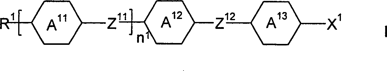
R1 Alkyl,
Alkoxy, bevorzugt n-Alkyl, n-Alkoxy, jeweils mit 1 bis 7 C-Atomen,
Alkenyl, Alkenyloxy, Alkinyl oder Alkoxyalkyl jeweils mit 2 bis
7 C-Atomen, 

X1 F, -OCF3, -CF3, -OCFZH, Cl, CN,
-C≡C-CN
oder NCS, bevorzugt CN, -C≡C-CN
oder NCS und
n1 0 oder 1 bedeuten,
wobei
im
Fall X1 = F die Phenylringe insgesamt mindestens
2, bevorzugt mindestens 3, weitere F-Atome tragen,
im Fall
X1 = -OCF3, -CF3, -OCF2H oder Cl
die Phenylringe insgesamt mindestens 1 weiteres F-Atom, bevorzugt mindestens
2 weitere, F-Atome tragen und
im Fall X1 =
CN, -C≡C-CN
oder NCS die Phenylringe bevorzugt mindestens 1 weiteres F-Atom tragen.Component A of these media preferably contains one or more compounds of the formula I and particularly preferably consists predominantly and very particularly preferably almost completely of one or more compounds of the formula I,
R 1 is alkyl, alkoxy, preferably n-alkyl, n-alkoxy, each having 1 to 7 C atoms, alkenyl, alkenyloxy, alkynyl or alkoxyalkyl each having 2 to 7 C atoms,
X 1 F, -OCF 3 , -CF 3 , -OCF Z H, Cl, CN, -C≡C-CN or NCS, preferably CN, -C≡C-CN or NCS and
n 1 denotes 0 or 1,
in which
in the case X 1 = F, the phenyl rings carry a total of at least 2, preferably at least 3, further F atoms,
in the case of X 1 = -OCF 3 , -CF 3 , -OCF 2 H or Cl, the phenyl rings carry a total of at least 1 further F atom, preferably at least 2 further F atoms, and
in the case of X 1 = CN, -C≡C-CN or NCS the phenyl rings preferably carry at least 1 further F atom.
Bevorzugt enthalten die erfindungsgemäßen Medien
eine oder mehrere Verbindungen ausgewählt aus der Gruppe der Verbindungen
der Formeln I-1 bis I-7 und/oder eine oder mehrere Verbindungen
ausgewählt
aus der Gruppe der Verbindungen der Formeln II-1 bis II-5, die ebenfalls
Teilformeln der Formel 1 sind. 
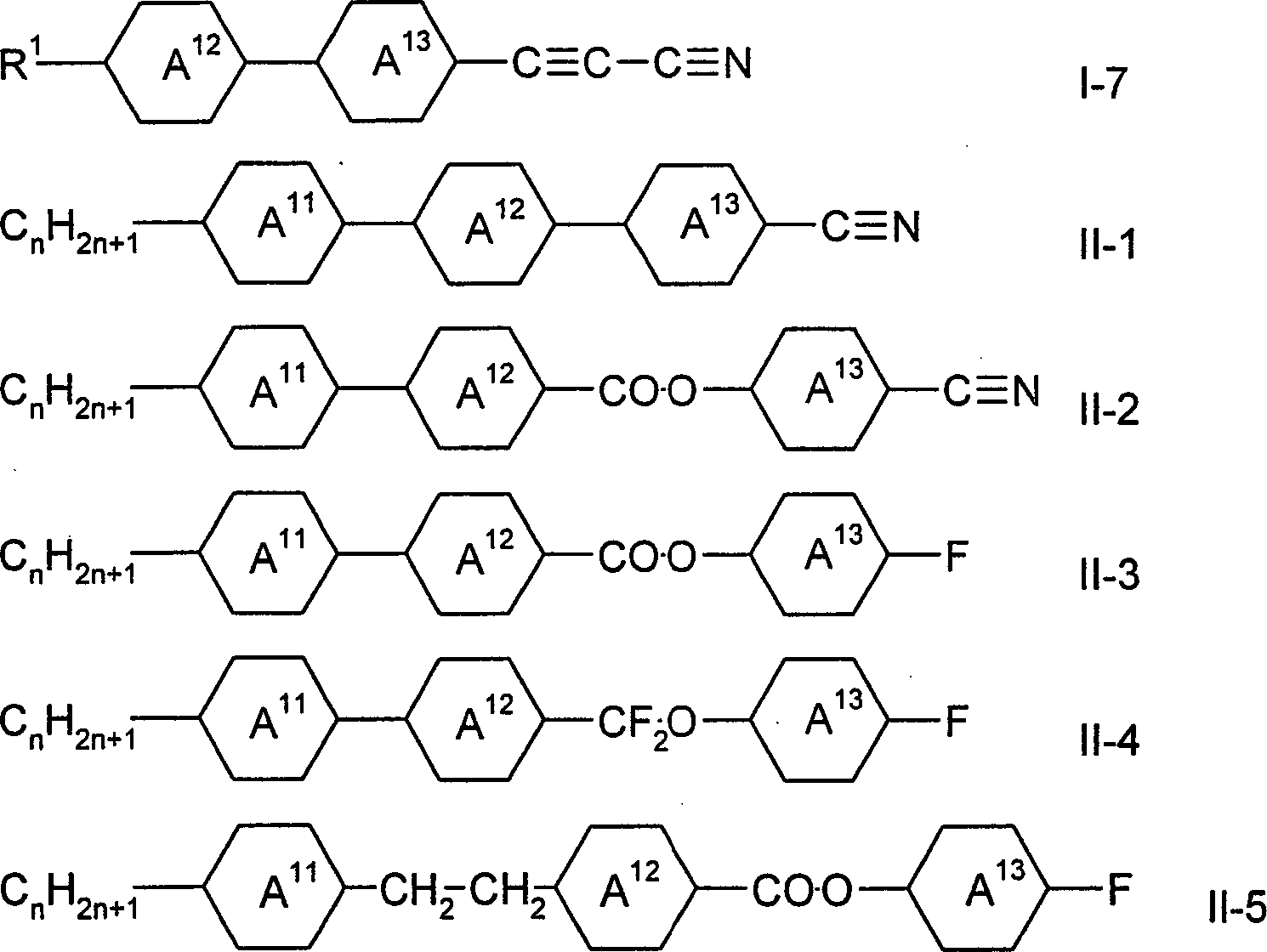
Besonders bevorzugt enthalten die
erfindungsgemäßen Medien
eine oder mehrere Verbindungen ausgewählt aus der Gruppe der Verbindungen
der Formeln I-1a bis I-1e, I-2a bis I-2c, I-3a bis I-3c, I-4a bis
I-4c, I-5a bis I-5c, I-6a bis I-6c und I-7a bis I-7c und/oder eine
oder mehrere Verbindungen ausgewählt
aus der Gruppe der Verbindungen der Formeln II-1a bis II-1c, II-2a
bis II-2c, II-3a, II3b, II-3a, II-4b, II-5a und II-5b. 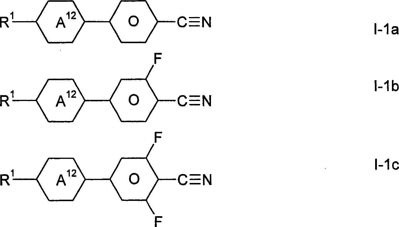
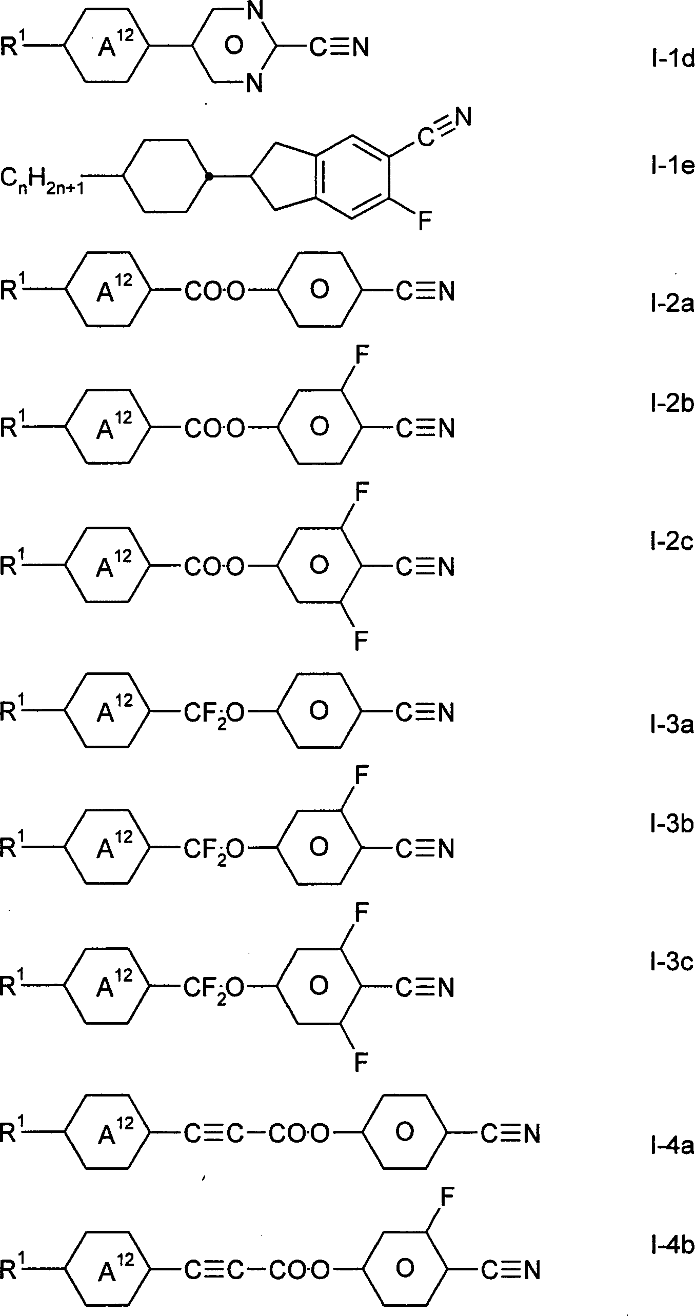

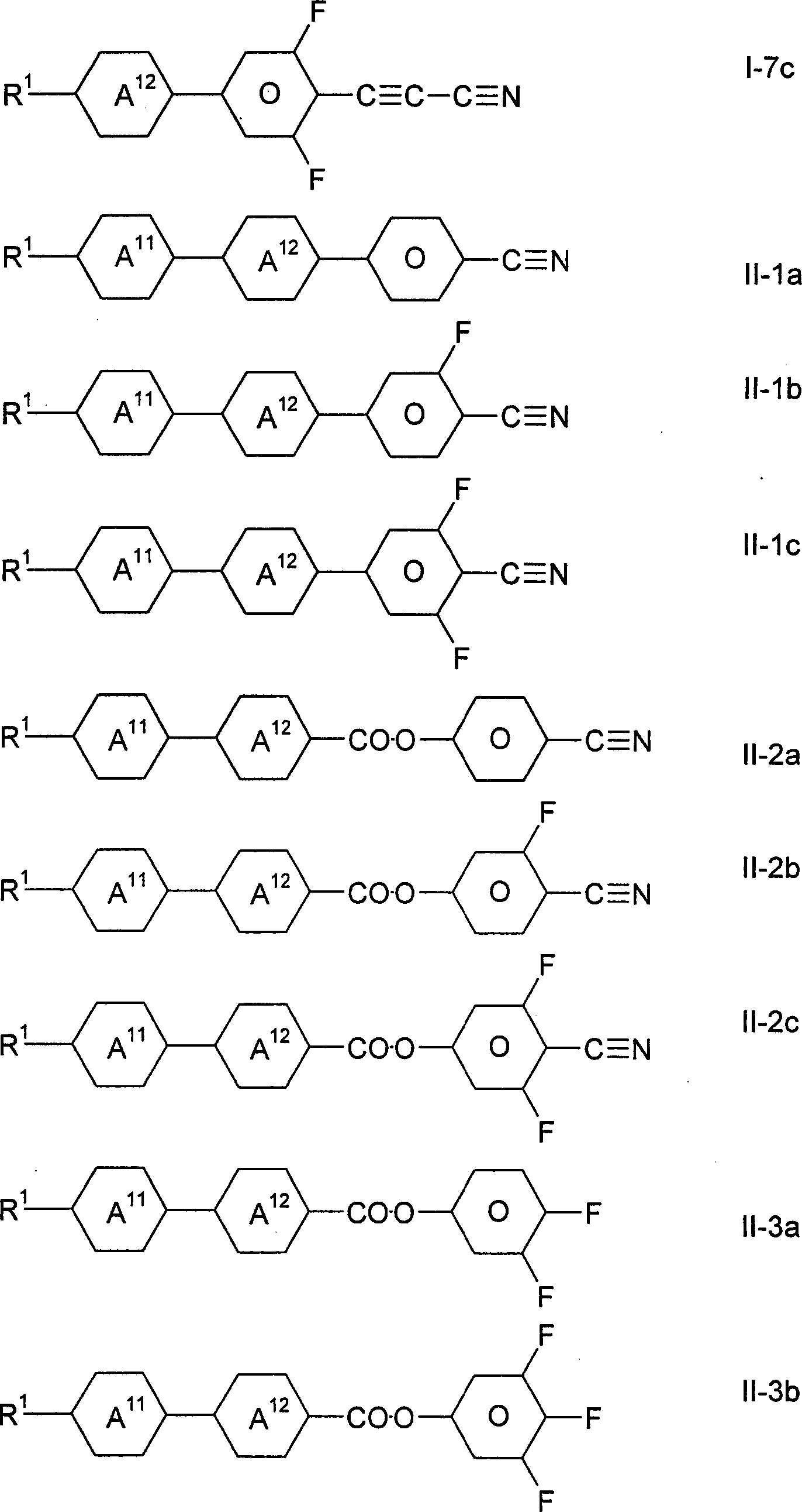
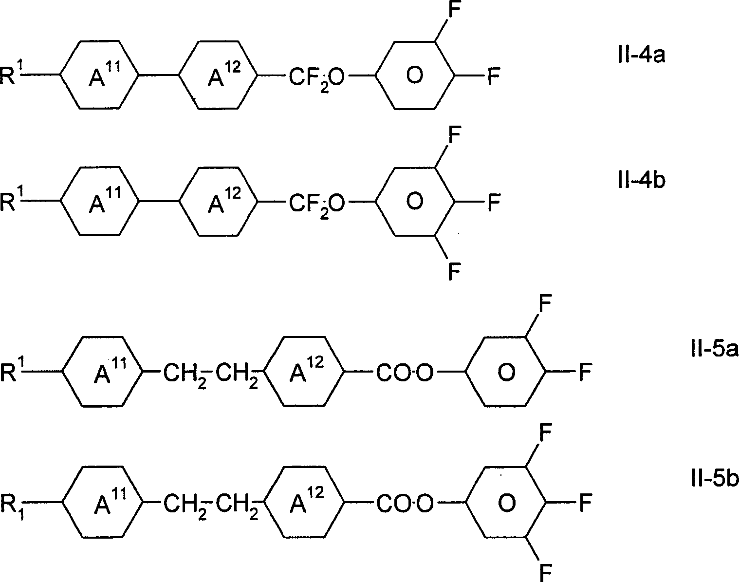
Die Verbindungen der Formeln I-1a
bis I-1e sind bevorzugt ausgesucht aus der Gruppe der Verbindungen
der Formeln I-1a-1 bis I-1a-6, I-1b-1 bis I-1b-9, I-1c-1 bis I-1c-9,
I-1d-1 bis I-1d-5 und I-1e-1 und I-1e-2. 
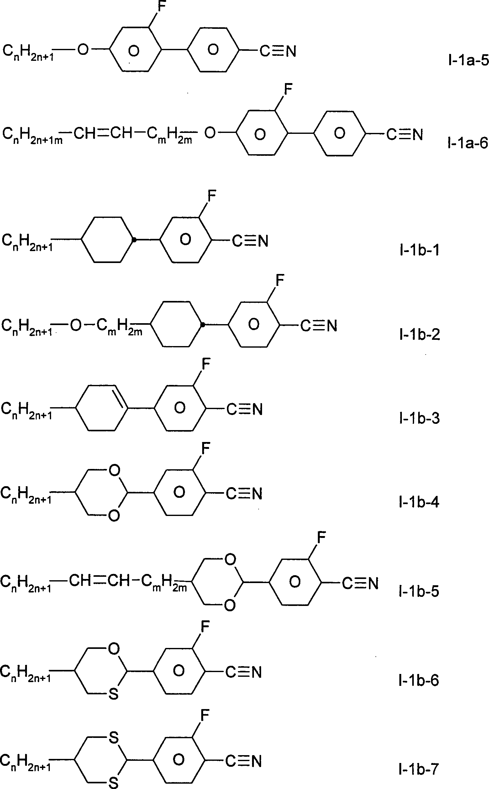

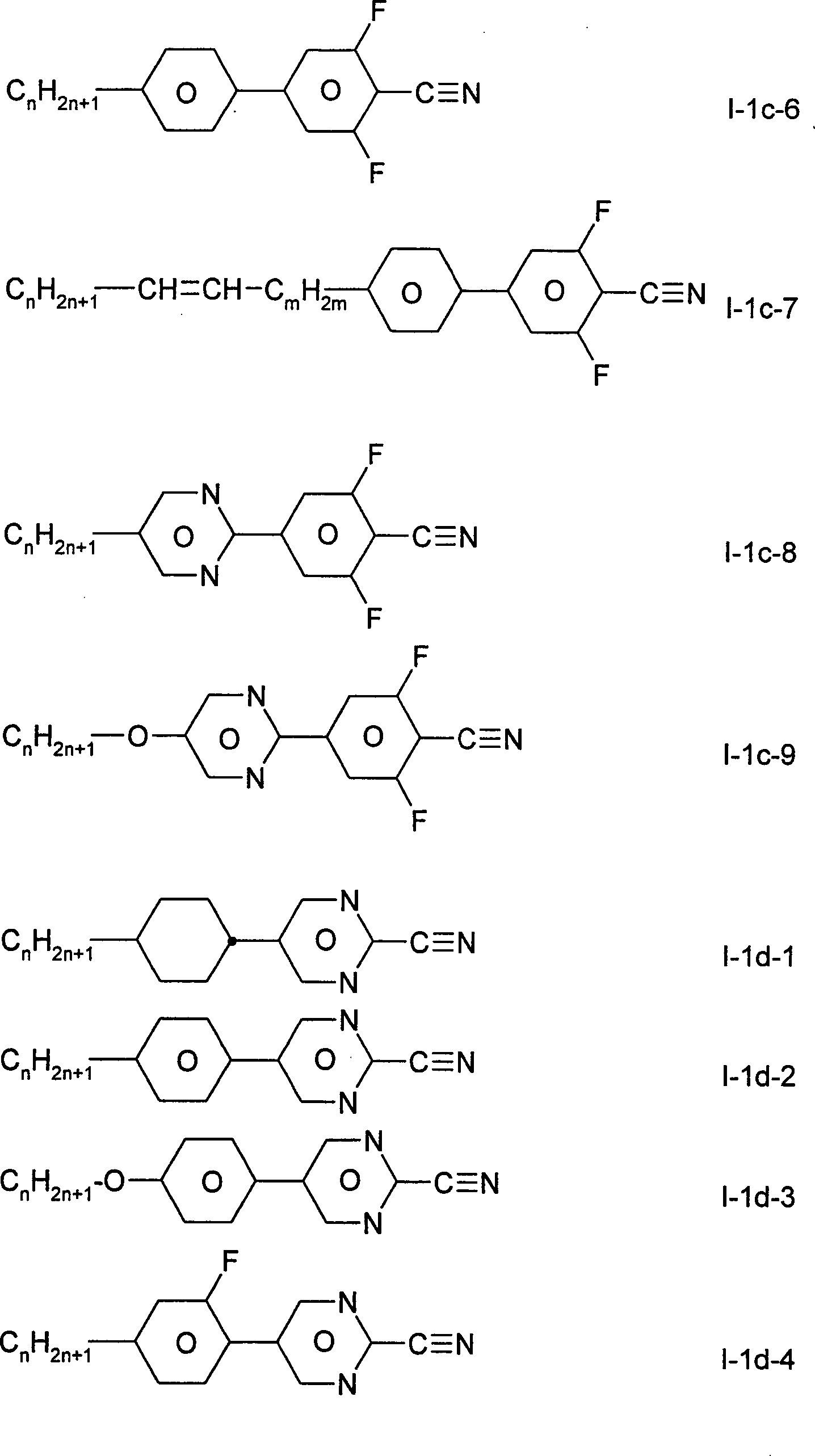

n
eine ganze Zahl von 0 bis 7, bevorzugt 1 bis 7,
m eine ganze
Zahl von 0 bis 5
n+m eine ganze Zahl von 0 bis 7, bevorzugt
von 1 bis 5
bedeuten.The compounds of the formulas I-1a to I-1e are preferably selected from the group of the compounds of the formulas I-1a-1 to I-1a-6, I-1b-1 to I-1b-9, I-1c-1 to I-1c-9, I-1d-1 to I-1d-5 and I-1e-1 and I-1e-2.
n is an integer from 0 to 7, preferably 1 to 7,
m is an integer from 0 to 5
n + m is an integer from 0 to 7, preferably from 1 to 5
mean.
Die Verbindungen der Formeln I-2a
bis I-2c sind bevorzugt ausgesucht aus der Gruppe der Verbindungen
der Formeln I-2a-1 bis I-2a-5, I-2b-1 bis I-2b-9 und I-2c-1 bis
I-2c-17. 
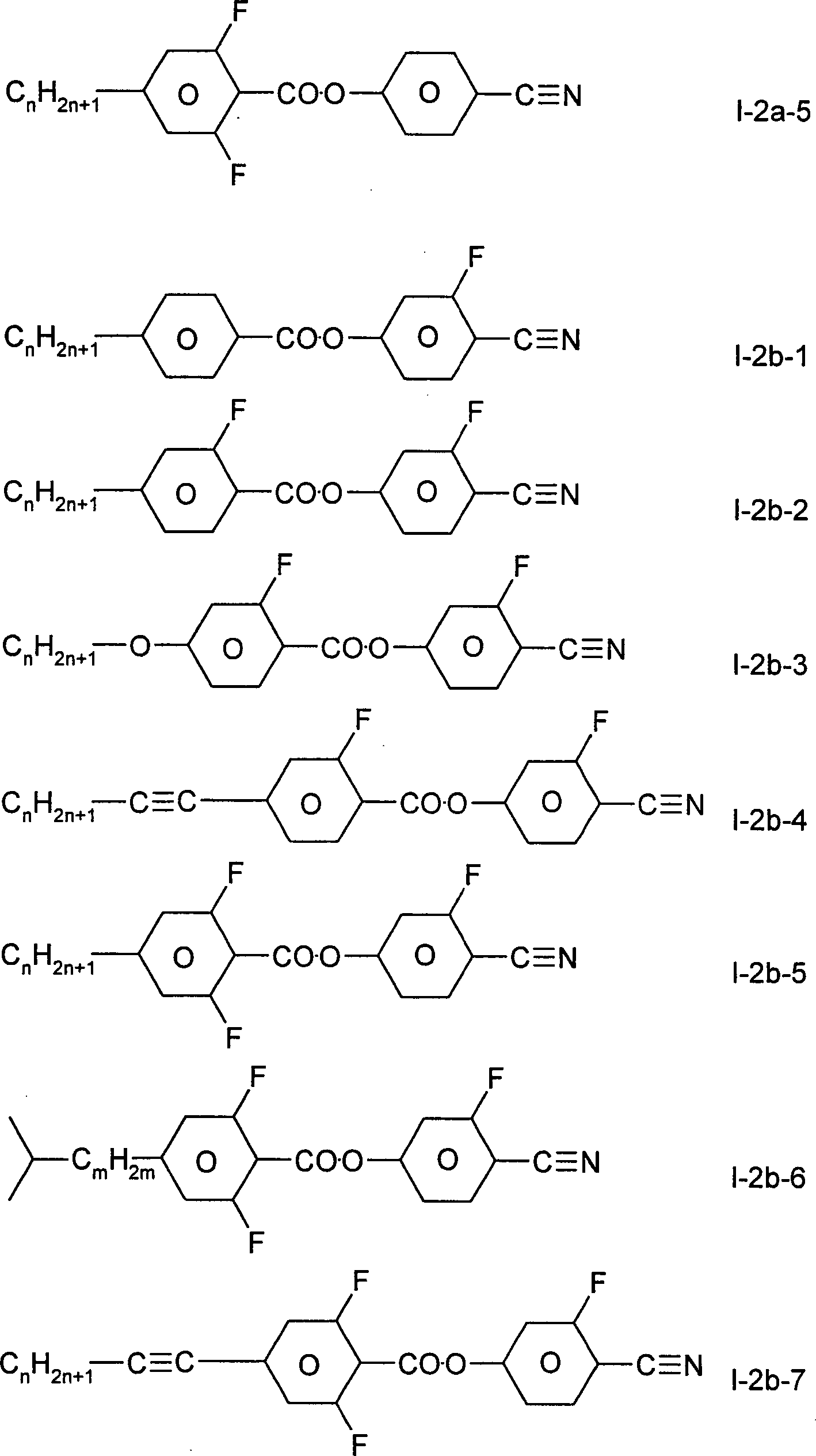

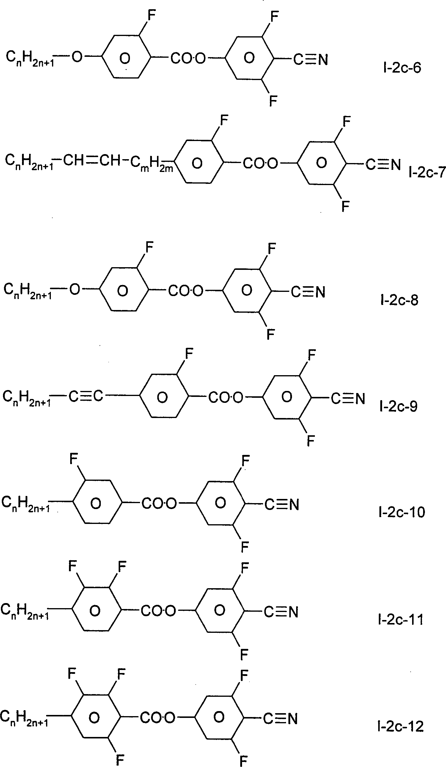

n
eine ganze Zahl von 0 bis 7, bevorzugt von 0 bis 5 und besonders
bevorzugt von 1 bis 5,
m eine ganze Zahl von 0 bis 5 und
n+m
eine ganze Zahl von 0 bis 7, bevorzugt von 1 bis 5
bedeutet.The compounds of the formulas I-2a to I-2c are preferably selected from the group of the compounds of the formulas I-2a-1 to I-2a-5, I-2b-1 to I-2b-9 and I-2c-1 to I-2c-17.
n is an integer from 0 to 7, preferably from 0 to 5 and particularly preferably from 1 to 5,
m is an integer from 0 to 5 and
n + m is an integer from 0 to 7, preferably from 1 to 5
means.
Die Verbindungen der Formeln I-3a
bis I-3c sind bevorzugt ausgesucht aus der Gruppe der Verbindungen
der Formeln I-3a-1 bis I-3a-4, I-3b-1 bis I-3b-4 und I-3c-1 bis
I-3c-4. 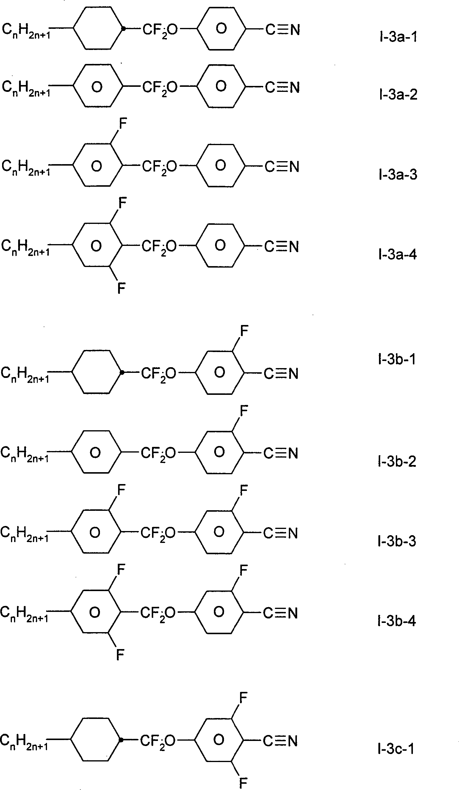
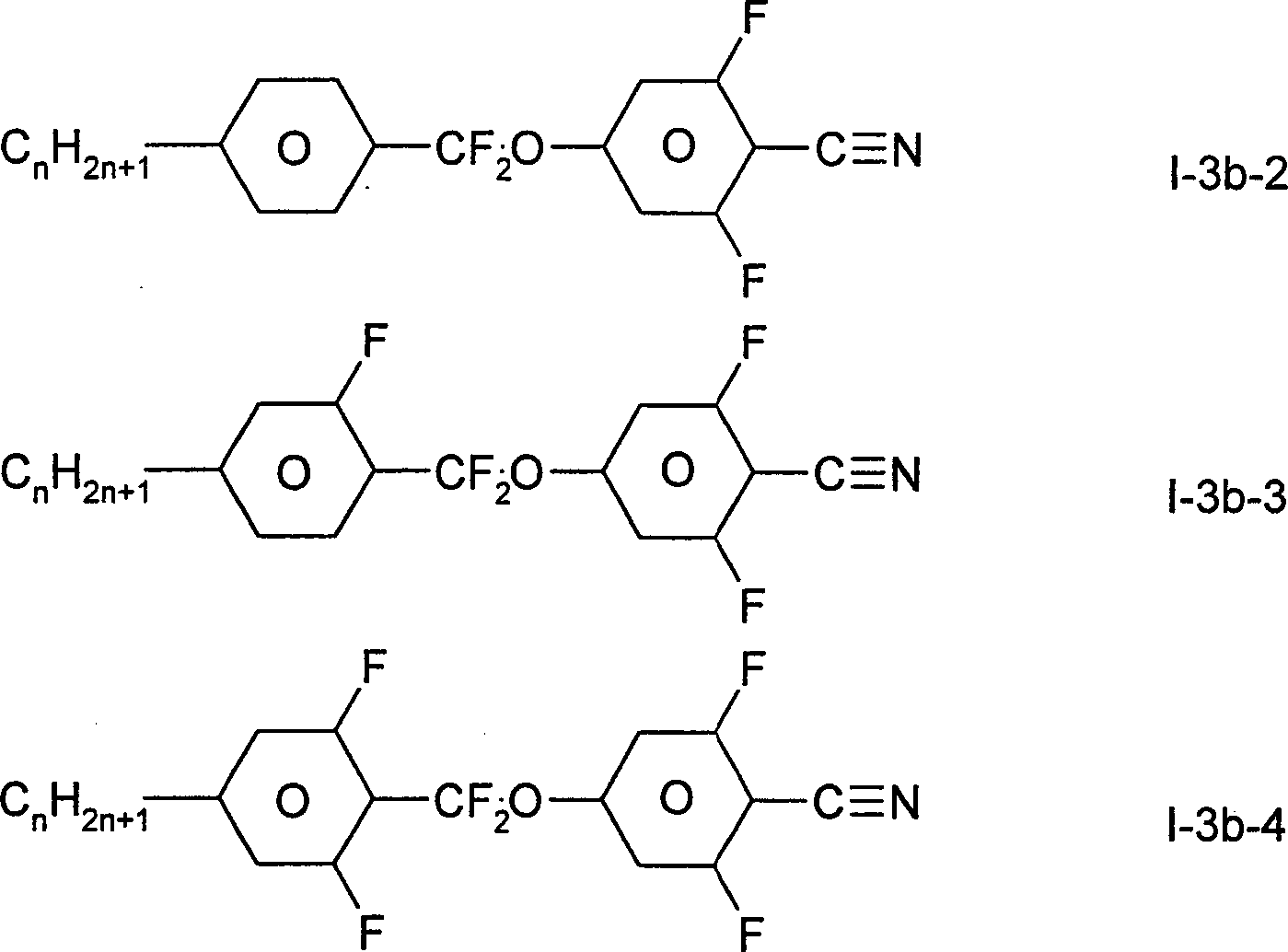
Die Verbindungen der Formeln I-4a
bis I-4c sind bevorzugt ausgesucht aus der Gruppe der Verbindungen
der Formeln I-4a-1 bis I-4a-3, I-4b-1 bis I-4b-3 und I-4e-1 bis
I-4c-3. 

Die Verbindungen der Formeln I-5a
bis I-5c sind bevorzugt ausgesucht aus der Gruppe der Verbindungen
der Formeln I-5a-1 b bis I-5a-3, I-5b-1 bis I-5b-3 und I-5c-1 bis
I-5a-1 I-5ca-3. 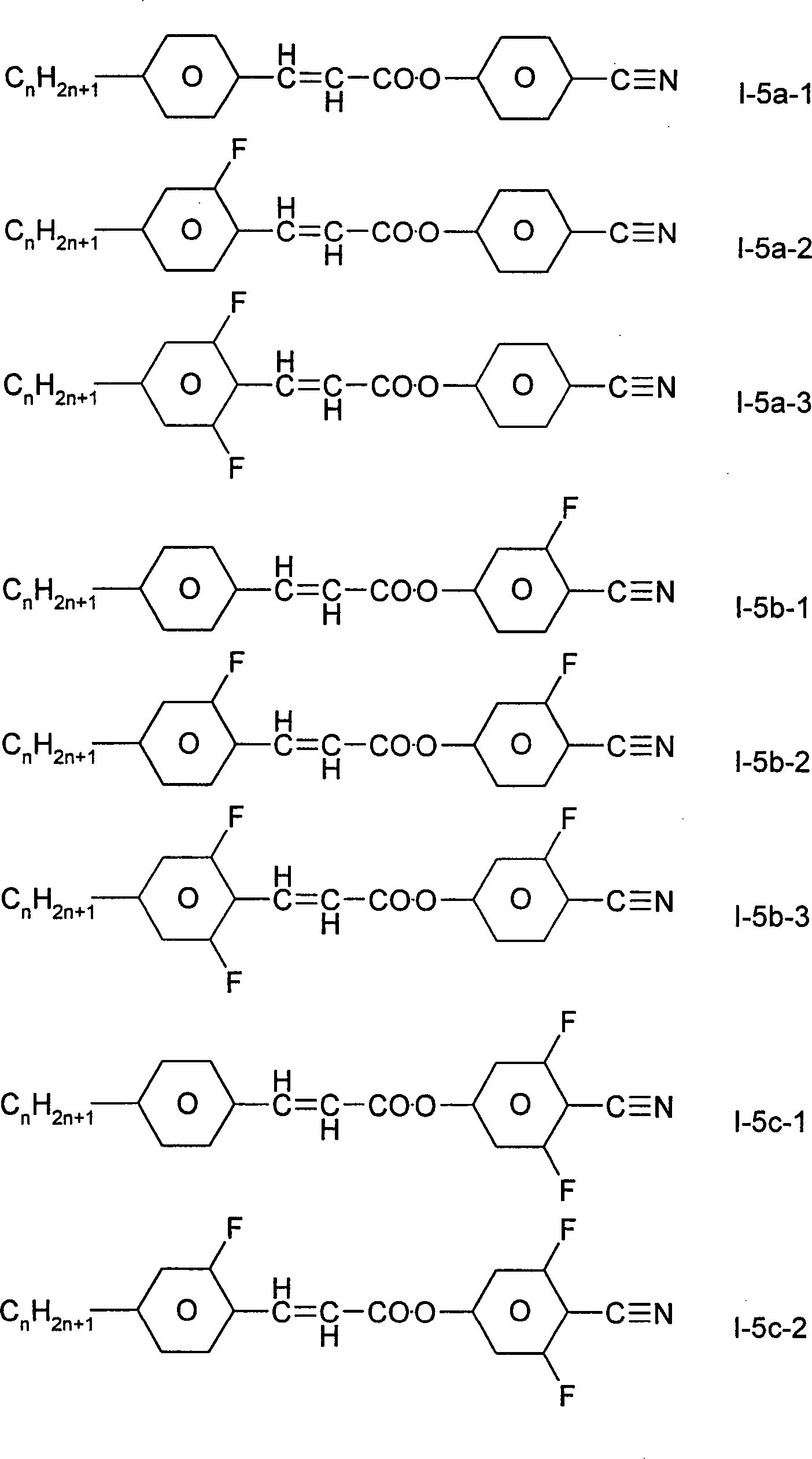

Die Verbindungen der Formeln I-6a
bis I-6c sind bevorzugt ausgesucht aus der Gruppe der Verbindungen
der Formeln I-6a-1 bis I-6a-3, I-6b-1 bis I-6a-3 und I-6c-1 bis
I-6a-3. 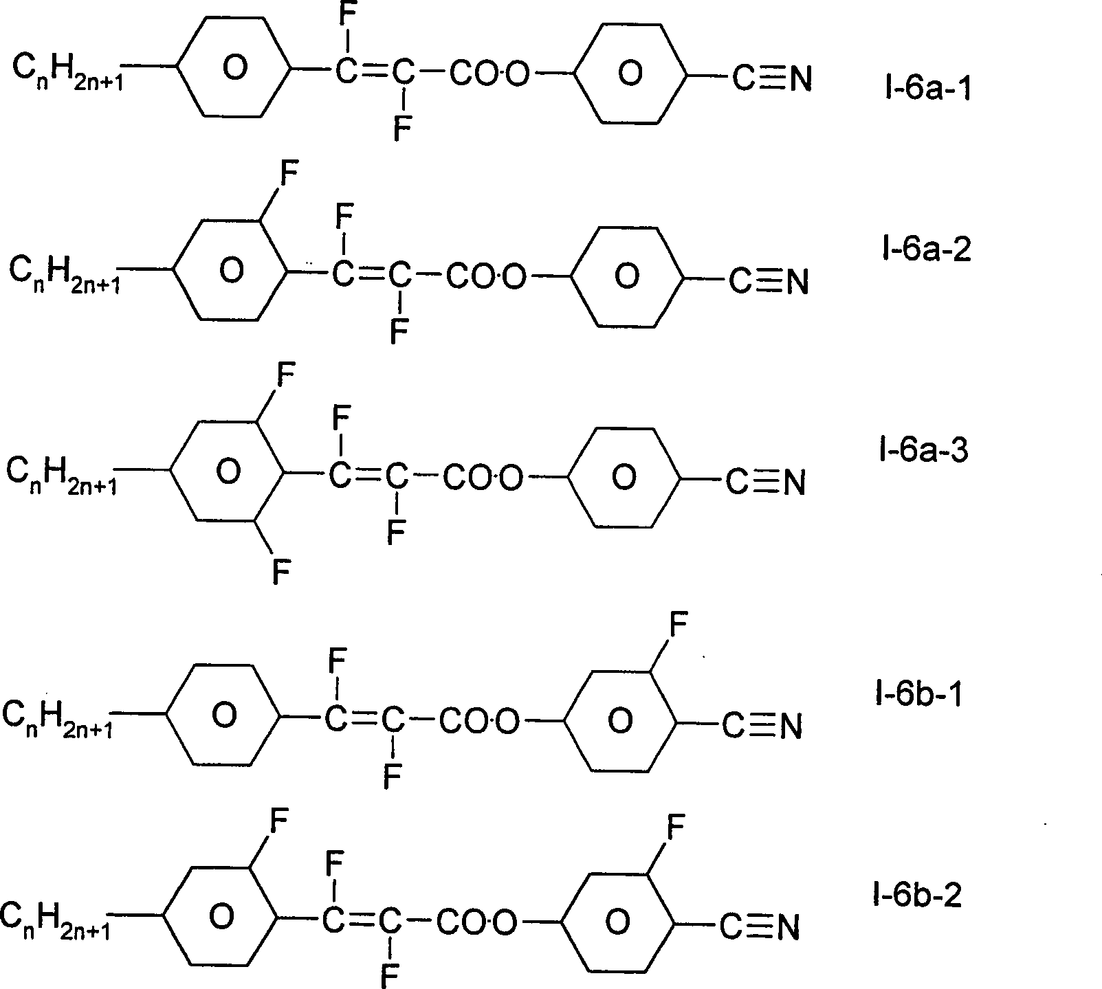

Die Verbindungen der Formeln I-7a
bis I-7c sind bevorzugt ausgesucht aus der Gruppe der Verbindungen
der Formeln I-7a-1 und I-7a-2, I-7b-1 und I-7b-2 und I-7c-1 und
I-7c-2. 
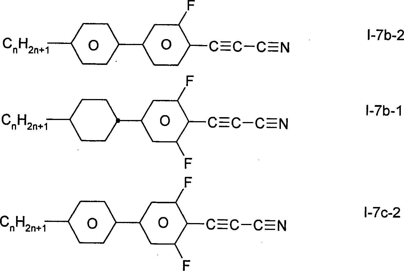
Besonders bevorzugt enthalten die
erfindungsgemäßen Medien
eine oder mehrere Verbindungen ausgewählt aus der Gruppe der Verbindungen
der Formeln II-1c-1, II-2c-1, II-3b-1, II-4b-1 und II-5b-1. 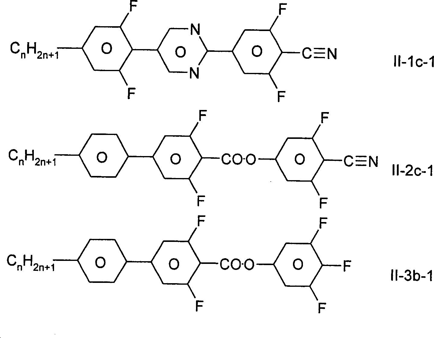
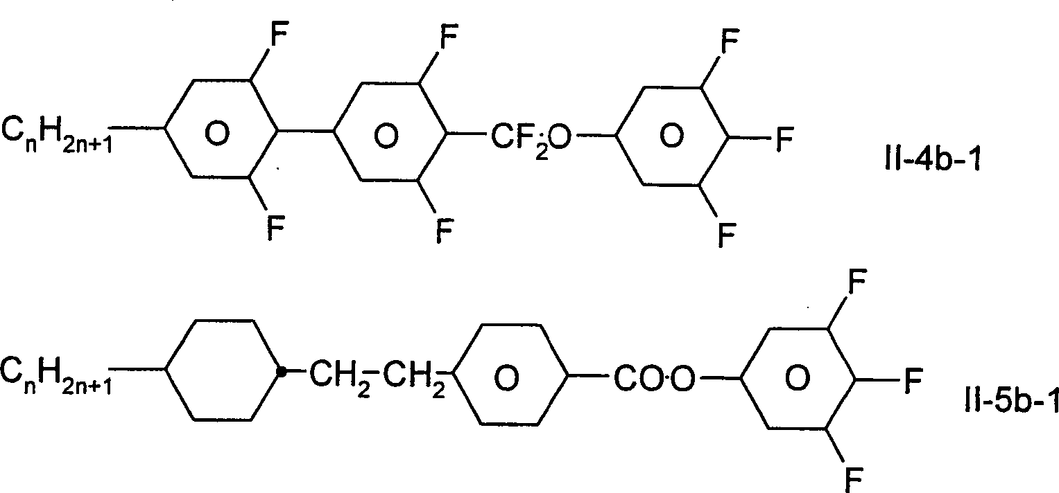
Bevorzugt enthalten die erfindungsgemäßen Medien eine oder mehrere Verbindungen ausgewählt aus der Gruppe der Verbindungen der Formeln I-1 bis I-7 und eine oder mehrere Verbindungen ausgewählt aus der Gruppe der Verbindungen der Formeln II-1 bis II-5.The media according to the invention preferably contain one or more compounds selected from the group of compounds of the formulas I-1 to I-7 and one or more compounds selected from the group of compounds of the formulas II-1 to II-5.
In der folgenden Tabelle sind einige Beispiele von Verbindungen der besonders bevorzugten Formeln zusammengestellt, die sich besonders zur Herstellung erfindungsgemäßer Medien eignen zusammengestellt.The following table are some Examples of compounds of the particularly preferred formulas compiled, which are particularly suitable for the production of media according to the invention.
Tabelle
1: Beispiele bevorzugter Verbindungen 
Tabelle
1 (Fortsetzung): Beispiele bevorzugter Verbindungen 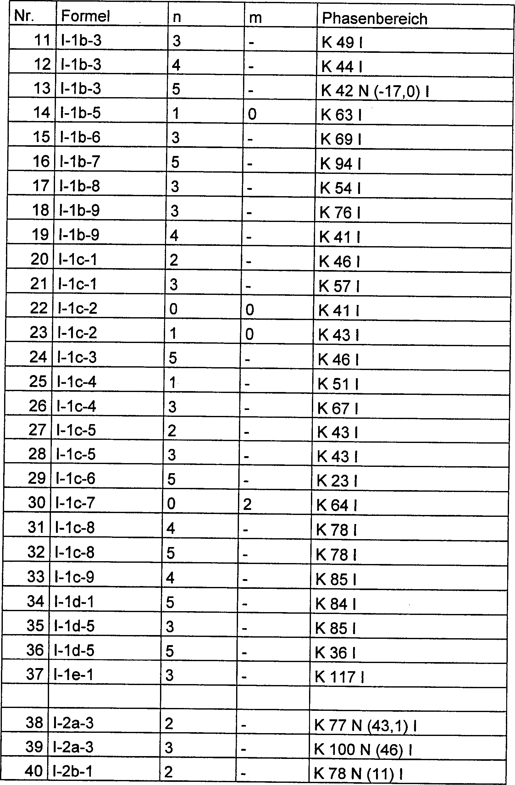
Tabelle
1 (Fortsetzung): Beispiele bevorzugter Verbindungen 
Tabelle
1 (Fortsetzung): Beispiele bevorzugter Verbindungen 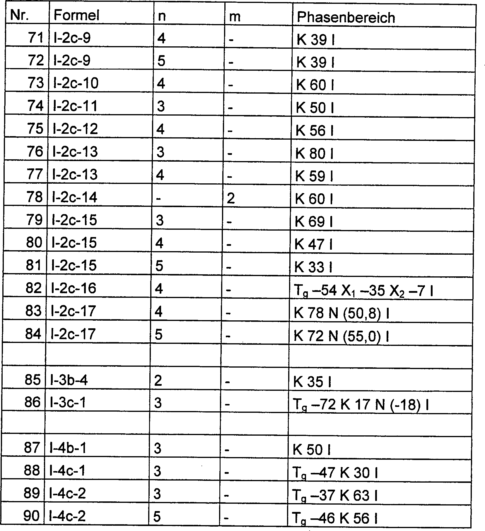
Tabelle
1 (Fortsetzung): Beispiele bevorzugter Verbindungen 
Die mesogenen Medien gemäß der vorliegenden Erfindung mit positiver dielektrischen Anisotropie bestehen besonders bevorzugt überwiegend und ganz besonders bevorzugt nahezu vollständig aus der Komponente A.The mesogenic media according to the present Invention with positive dielectric anisotropy exist particularly preferably predominantly and very particularly preferably almost completely from component A.
In einer bevorzugten Ausführungsform enthalten die mesogenen Medien gemäß der vorliegenden Erfindung mit positiver dielektrischer Anisotropie eine oder mehrere Komponenten ausgewählt aus der Gruppe der Komponenten B bis D, bevorzugt ausgewählt aus der Gruppe der Komponenten B und D.In a preferred embodiment contain the mesogenic media according to the present invention with positive dielectric anisotropy one or more components selected from the group of components B to D, preferably selected from the group of components B and D.
Die Komponente D dieser Medien enthält bevorzugt eine oder mehrere Verbindungen. Die mesogenen Medien mit negativer dielektrischen Anisotropie gemäß der vorliegenden Erfindung enthalten bevorzugt
- – eine Komponente A' bestehend aus einer oder mehreren Verbindungen mit einer stark negativen dielektrischen Anisotropie von –5 oder weniger,
- – optional eine Komponente B' bestehend aus einer oder mehreren Verbindungen mit einer moderat negativen dielektrischen Anisotropie von –1,5 bis < –5,
- – optional eine Komponente C' bestehend aus einer oder mehreren dielektrisch neutralen Verbindungen mit einer dielektrischen Anisotropie von –1,5 bis +1,5 und
- – gegebenenfalls eine Komponente D' bestehend aus einer oder mehreren Verbindungen mit einer positiven dielektrischen Anisotropie von mehr als 1,5.
- A component A 'consisting of one or more compounds with a strongly negative dielectric anisotropy of -5 or less,
- Optionally a component B 'consisting of one or more compounds with a moderately negative dielectric anisotropy from -1.5 to <-5,
- - Optionally a component C 'consisting of one or more dielectrically neutral compounds with a dielectric anisotropy of -1.5 to +1.5 and
- - optionally a component D 'consisting of one or more compounds with a positive dielectric anisotropy of more than 1.5.
Das mesogene Medium gemäß der vorliegenden Erfindung kann weitere Additive und chirale Dotierstoffe in üblichen Konzentrationen enthalten. Die Gesamtkonzentration dieser weiteren Bestandteile liegt im Bereich von 0% bis 10%, bevorzugt im Bereich von 0,.1 % bis 6%, bezogen auf die Gesamtmischung. Die Konzentrationen der einzelnen dieser Verbindungen liegen im Bereich von 0,1 bis 3%. Die Konzentration dieser Verbindungen und ähnlicher Bestandteile der Mischung werden bei der Angabe der Konzentrationsbereiche der übrigen Mischungsbestandteile nicht berücksichtigt.The mesogenic medium according to the present invention can contain further additives and chiral dopants in conventional concentrations. The total concentration of these further constituents is in the range from 0% to 10%, preferably in the range from 0.1% to 6%, based on the total mixture. The concentrations of the individual of these compounds are in the range from 0.1 to 3%. The concentration of these compounds and similar components of the mixture are given when specifying the concentration ranges the other components of the mixture are not taken into account.
Die Medien werden auf übliche Weise aus den Verbindungen erhalten. Zweckmäßiger Weise werden die Verbindungen die in geringerer Menge eingesetzt werden in den in größerer Menge eingesetzten Verbindungen gelöst. Wird die Temperatur während des Mischvorgangs über den Klärpunkt der überwiegenden Komponente erhöht, kann die Vollständigkeit der Auflösung leicht beobachtet werden. Die erfindungsgemäßen Medien können jedoch auch auf andere Weisen hergestellt werden. So durch den Einsatz von Vormischungen. Als Vormischungen könne unter anderem Homologenmischungen und/oder eutektische Mischungen eingesetzt werden. Die Vormischungen können aber auch bereits selbst einsatzfähige Medien sein. Dies ist bei sogenannten Zwei- oder Mehr-Flaschen-Systemen (Englisch: two-bottle or multi-bottle systems) der Fall.)The media are made in the usual way obtained from the connections. The connections are expedient which are used in smaller quantities in larger quantities used connections solved. Will the temperature during of the mixing process the clearing point the predominant Component increased, can completeness the dissolution can be easily observed. However, the media according to the invention can can also be made in other ways. So through the effort of premixes. Homolog mixtures can be used as premixes and / or eutectic mixtures are used. The premixes can but also be usable media itself. This is in so-called two-bottle or multi-bottle systems (English: two-bottle or multi-bottle systems) the case.)
In der vorliegenden Anmeldung gilt, soweit nicht explizit anders angegeben, das Folgende.In the present application, unless explicitly stated otherwise, the following.
Dielektrisch positive Verbindungen haben ein Δε > 1,5, dielektrisch neutrale Verbindungen haben ein Δε im Bereich –1,5 ≤ 5 Δε ≤ 1,5 und dielektrisch negative Verbindungen haben ein Δε < –1,5. Die selben Definitionen gelten auch für Komponenten von Mischungen und für Mischungen.Dielectric positive connections have a Δε> 1.5, dielectric neutral connections have a Δε in the range –1.5 ≤ 5 Δε ≤ 1.5 and dielectric negative compounds have a Δε <-1.5. The The same definitions also apply to components of mixtures and for Mixtures.
Die dielektrische Anisotropie Δε der Verbindungen wird bei 1 kHz und 20°C durch Extrapolation der Werte einer 10%-igen Lösung der jeweiligen Verbindung in einer Wirtsmischung auf einen Anteil der jeweiligen Verbindung von 100% bestimmt. Die Kapazitäten der Testmischungen werden sowohl in einer Zelle mit homeotroper, als auch in einer Zelle mit homogener Randorientierung bestimmt. Die Schichtdicke beider Zellentypen beträgt circa 20 μm. Zur Messung wird eine Rechteckwelle mit einer Frequenz von 1 kHz und einer effektiven Spannung (rms, Englisch: root mean square) von typischer Weise 0.2 V bis 1.0 V verwendet. In jedem Fall ist die verwendete Spannung niedriger als die kapazitive Schwelle der jeweils untersuchten Mischung.The dielectric anisotropy Δε of the connections is at 1 kHz and 20 ° C by extrapolating the values of a 10% solution of the respective compound in a host mixture on a portion of the respective compound determined by 100%. The capacities of the test mixtures are both in a cell with homeotropic, as well as in a cell with a homogeneous edge orientation. The layer thickness of both cell types is approximately 20 μm. For measurement becomes a square wave with a frequency of 1 kHz and an effective voltage (rms, English: root mean square) of typically 0.2 V to 1.0 V used. In any case, the voltage used is lower than the capacitive threshold of the mixture examined in each case.
Für dielektrisch positive Verbindungen wird die Mischung ZLI-4792 und für dielektrisch neutrale, sowie für dielektrisch negative Verbindungen, die Mischung ZLI-3086, beide von Merck KGaA, Deutschland, als Wirtsmischung verwendet.For the mixture ZLI-4792 and dielectric positive connections for dielectric neutral, as well as for dielectric negative compounds, the mixture ZLI-3086, both from Merck KGaA, Germany, used as the host mixture.
Der Begriff Schwellenspannung bedeutet in der vorliegenden Anmeldung die optische Schwelle und wird für einen relativen Kontrast von 10 % (V10) angegeben. Die Mittgrauspannung und die Sättigungsspannung werden ebenfalls optisch bestimmt und für einen relativen Kontrast von 50%, bzw. von 90 % angegeben. Die kapazitive Schwellenspannung (V0), auch Freedericksz-Schwelle genannt, angegeben, so wird dies explizit angegeben.In the present application, the term threshold voltage means the optical threshold and is indicated for a relative contrast of 10% (V 10 ). The mid-gray voltage and the saturation voltage are also determined optically and specified for a relative contrast of 50% and 90%, respectively. The capacitive threshold voltage (V 0 ), also called the Freedericksz threshold, is given, so this is stated explicitly.
Die angegebenen Bereiche von Werten schließen die Grenzwerte ein.The specified ranges of values conclude the limits.
Die Konzentrationen sind in Massen-% gegeben und beziehen sich auf die vollständige Mischung. Temperaturen sind in Grad Celsius und Temperaturdifferenzen in Differenzgrad Celsius angegeben. Alle physikalischen Eigenschaften wurden bestimmt wie in "Merck Liquid Crystals, Physical Properties of Liquid Crystals", Stand Nov. 1997, Merck KGaA, Deutschland und sind für eine Temperatur von 20 °C angegeben. Die optische Anisotropie (Δn), auch Doppelbrechung genannt, wird bei einer Wellenlänge von 589,3 nm bestimmt. Die dielektrische Anisotropie (Δε) wird bei einer Frequenz von 1 kHz bestimmt.The concentrations are in mass% given and refer to the complete mix. temperatures are in degrees Celsius and temperature differences in degrees of difference Celsius specified. All physical properties were determined as in "Merck Liquid Crystals, Physical Properties of Liquid Crystals", As of Nov. 1997, Merck KGaA, Germany and are for one temperature of 20 ° C specified. Optical anisotropy (Δn), also called birefringence, becomes at a wavelength determined from 589.3 nm. The dielectric anisotropy (Δε) is at determined at a frequency of 1 kHz.
In einer Aufzählung alternativer Möglichkeiten bedeutet bei Angabe nur des Plurals dieser auch den Singular.In a list of alternative options if only the plural is specified, this also means the singular.
Im Zusammenhang mit Angaben zur Zusammensetzung der Medien, bzw. ihrer Komponenten, bedeutet
- – „enthalten", dass die Konzentration des jeweiligen genannten Materials, also der Komponente oder der Verbindung, in der Bezugseinheit, also dem Medium bzw. der Komponente, bevorzugt 10% oder mehr, besonders bevorzugt 20 % oder mehr und ganz besonders bevorzugt 30% oder mehr beträgt,
- – „überwiegend bestehen aus", dass die Konzentration des genannten Materials in der Bezugseinheit bevorzugt 50% oder mehr, besonders bevorzugt 60 % oder mehr und ganz besonders bevorzugt 70% oder mehr beträgt und
- – „nahezu vollständig bestehen aus", dass die Konzentration des genannten Materials in der Bezugseinheit bevorzugt 80% oder mehr, besonders bevorzugt 90 % oder mehr und ganz besonders bevorzugt 95% oder mehr beträgt.
- - "contain" that the concentration of the respective material mentioned, ie the component or the compound, in the reference unit, ie the medium or the component, preferably 10% or more, particularly preferably 20% or more and very particularly preferably 30% or more,
- "Predominantly consist of" that the concentration of the material mentioned in the reference unit is preferably 50% or more, particularly preferably 60% or more and very particularly preferably 70% or more and
- "Almost completely consist of" that the concentration of the material mentioned in the reference unit is preferably 80% or more, particularly preferably 90% or more and very particularly preferably 95% or more.
Die dielektrischen Eigenschaften, elektrooptischen Eigenschaften (z.B. die Schwellenspannungen) und die Schaltzeiten wurden in bei der Merck KGaA, Darmstadt, Deutschland hergestellten Testzellen, bestimmt. Die Testzellen zur Bestimmung von Δε hatten eine Schichtdicke von 22 μm und eine kreisförmige Elektrode aus Indiumzinnoxid (ITO) mit einer Fläche von 1,13 cm2 und einem Schutzring. Für homeotrope Orientierung zu Bestimmung von ε|| wurden Zellen mit einer homeotrop orientierenden Polyimid-Orientierungsschicht verwendet. Alternativ kann Lezithin (Merck KGaA) als Orientierungsmittel verwendet. Die Zellen zur Bestimmung von ε⫠ hatten Orientierungsschichten aus dem Polyimid AL-1054 der Firma Japan Synthetic Rubber, Japan. Die Kapazitäten wurden in der Regel mit einem Frequenzanalysator Solatron 1260 mit einer Rechteckwelle mit einer Effektivspannung von 0.3 Vrms gemessen. Die elektooptischen Untersuchungen wurden mit weißem Licht durchgeführt. Die charakteristischen Spannungen wurden unter senkrechter Beobachtung bestimmt.The dielectric properties, electro-optical properties (eg the threshold voltages) and the switching times were determined in test cells manufactured by Merck KGaA, Darmstadt, Germany. The test cells for determining Δε had a layer thickness of 22 μm and a circular electrode made of indium tin oxide (ITO) with an area of 1.13 cm 2 and a protective ring. For homeotropic orientation to determine ε || cells with a homeotropically oriented polyimide orientation layer were used. Alternatively, lecithin (Merck KGaA) can be used as an orientation aid. The cells for determining ε ε had orientation layers made of the polyimide AL-1054 from Japan Synthetic Rubber, Japan. The capacitances were generally measured with a Solatron 1260 frequency analyzer with a square wave with an effective voltage of 0.3 V rms . The electro-optical examinations were carried out with white light. The characteristic tensions were determined under vertical observation.
In der vorliegenden Anmeldung, besonders
in den im folgenden beschriebenen Beispielen werden die Strukturen
der chemischen Verbindungen mittels Abkürzungen angegeben. Die Bedeutung
der jeweiligen Abkürzungen
ist in den folgenden Tabellen A und B zusammengestellt. Alle Gruppen
CnH2n+1 und CmH2m+1 sind geradkettige
Alkylgruppen mit n bzw. m C-Atomen. Tabelle B ist aus sich selbst
heraus verständlich,
da sie jeweils die vollständige
Abkürzung
für eine
Formel homologer Verbindungen angibt. In Tabelle A sind nur die Abkürzungen
für die
Kernstrukturen der Verbindungstypen zusammengestellt. Die Abkürzungen
für die
jeweiligen einzelnen Verbindungen setzen sich aus der jeweils zutreffenden
dieser Abkürzungen
für den
Kern der Verbindung und der mittels einem Bindestrich angehängten Abkürzung für die Gruppen
R1, R2, L1 und L2 gemäß folgender
Tabelle zusammen. 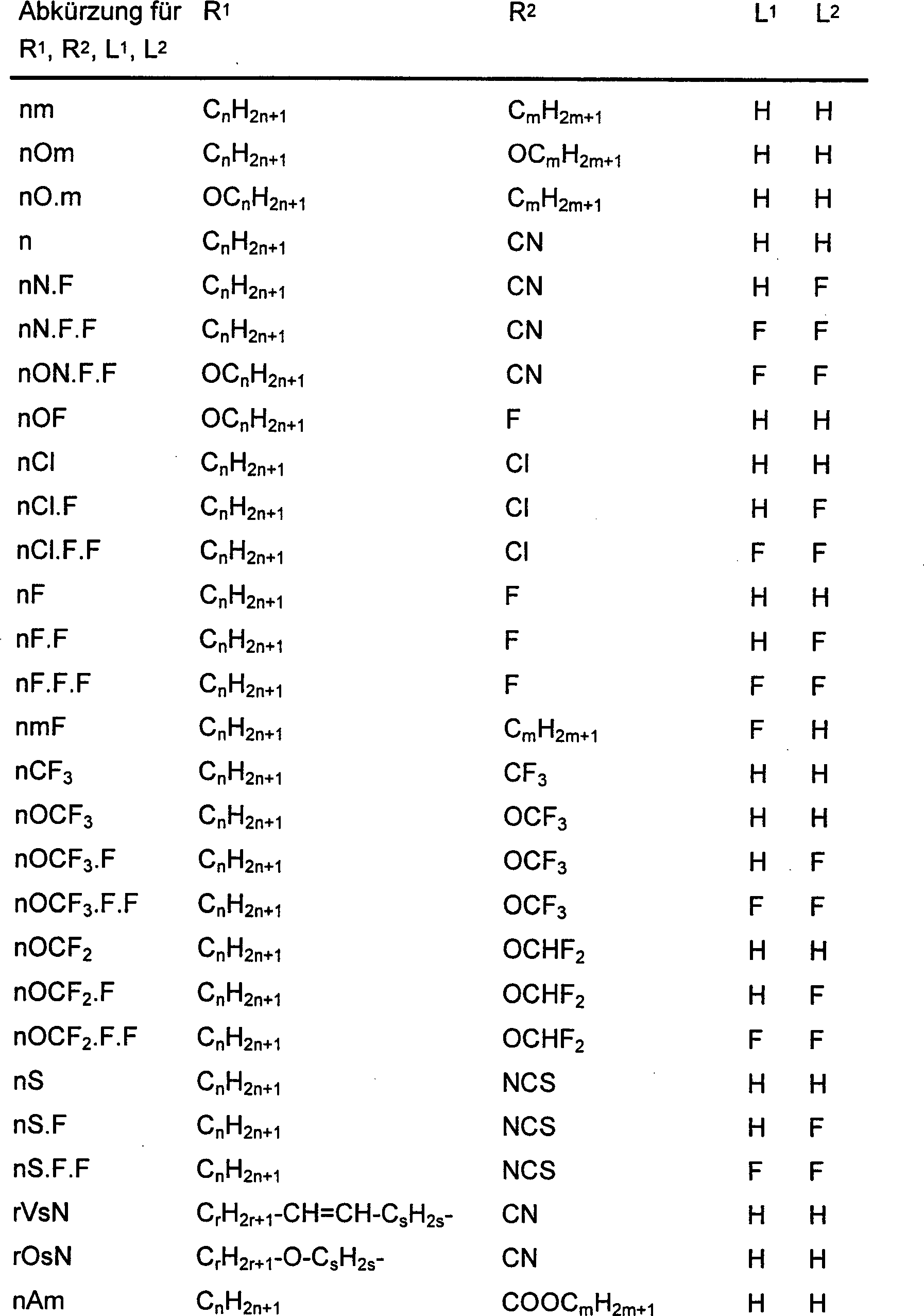

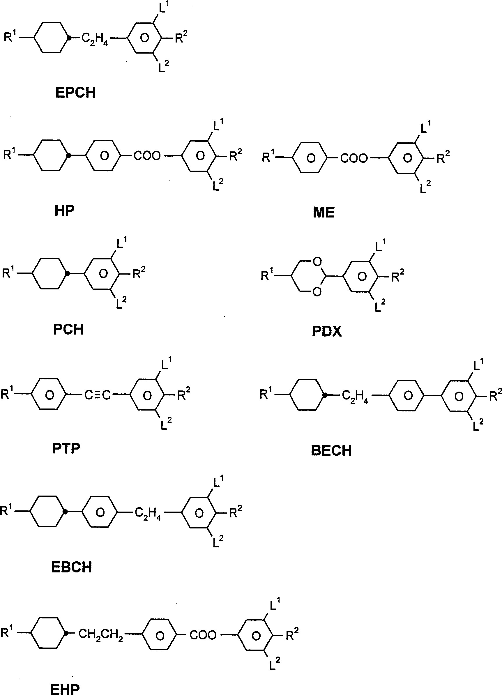

Table
B: 

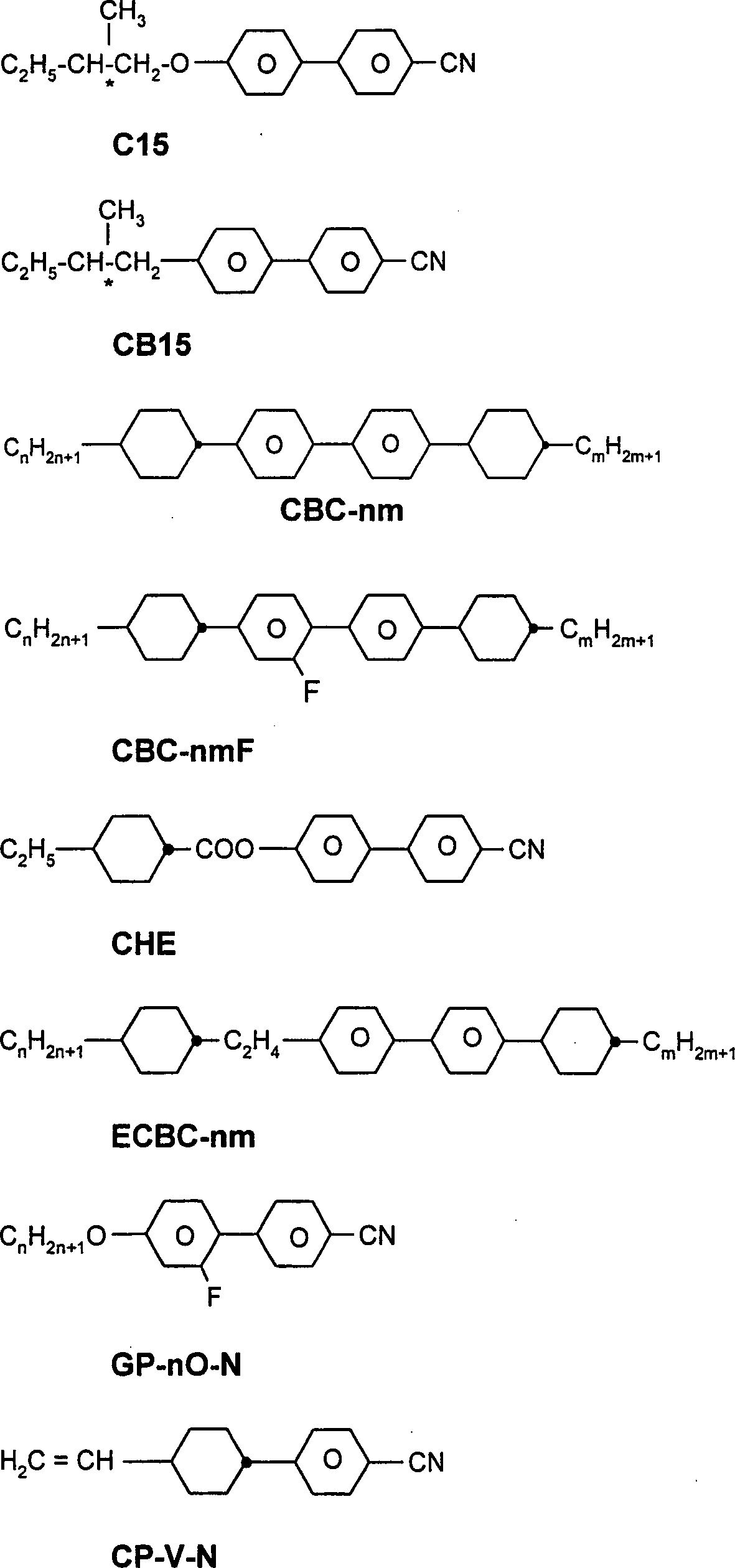

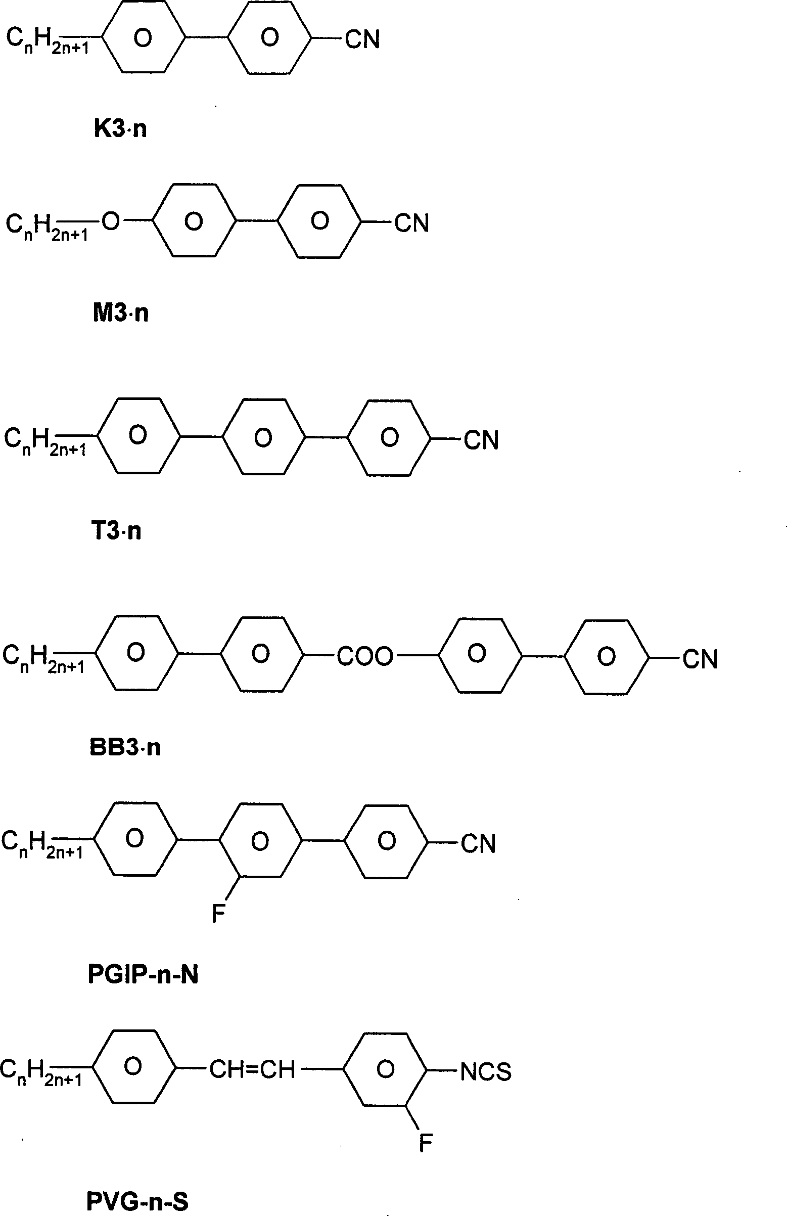
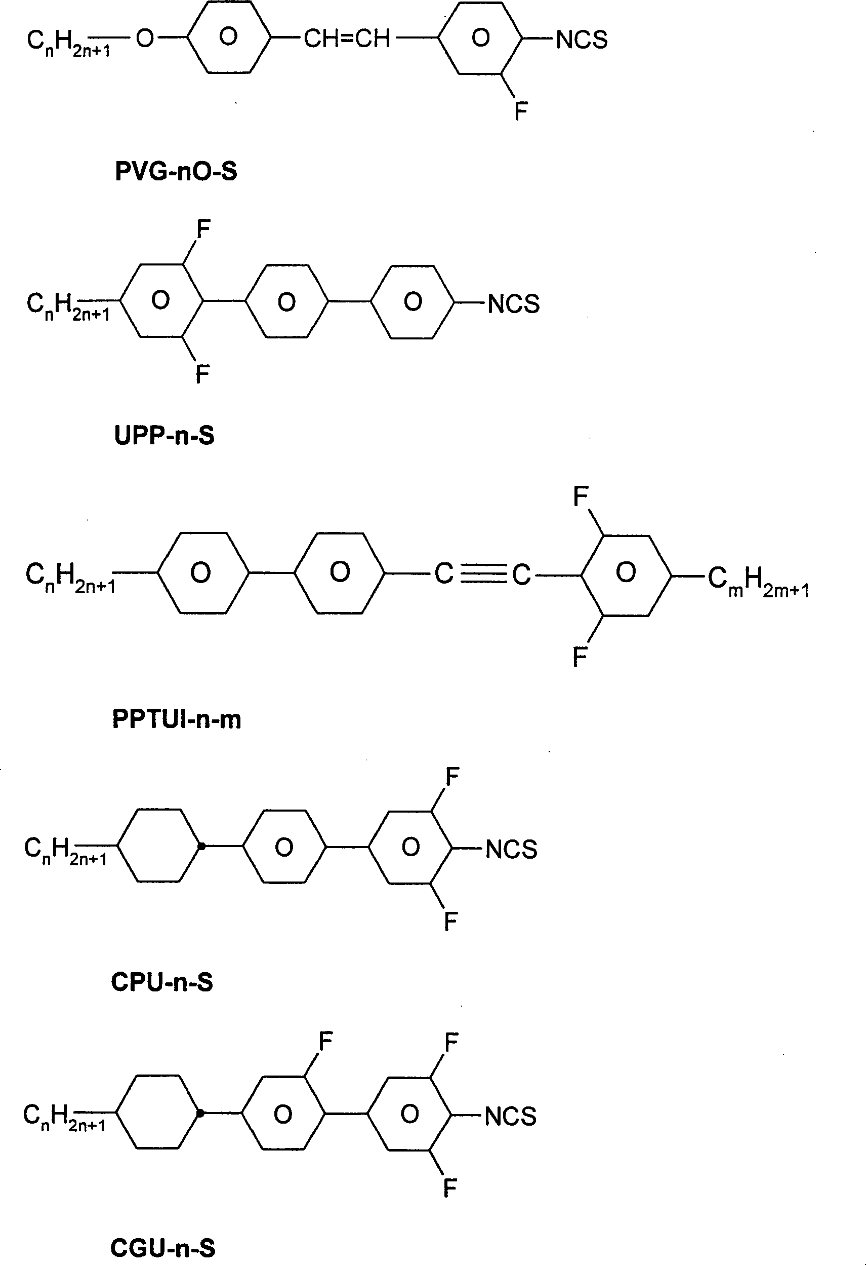


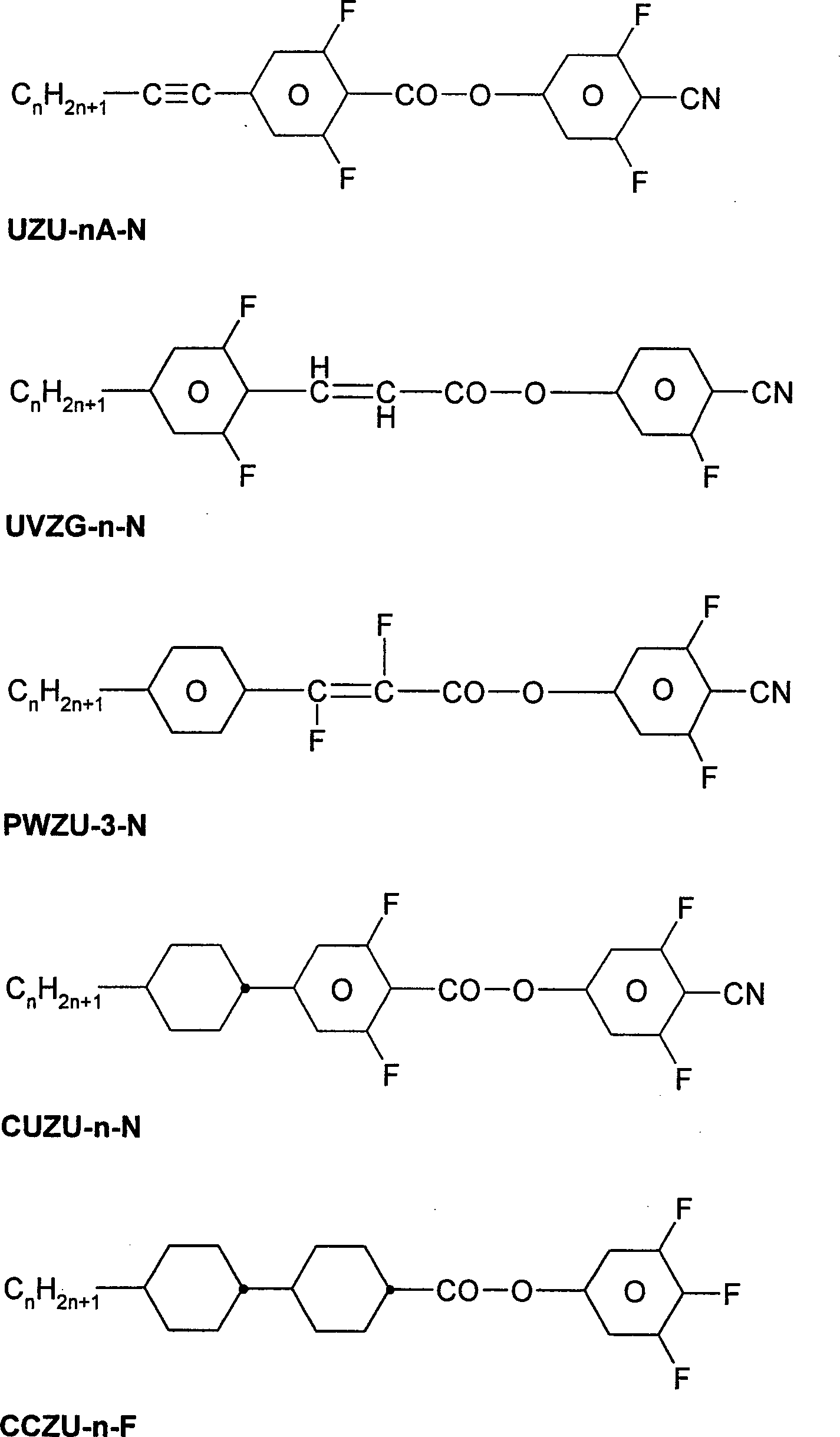
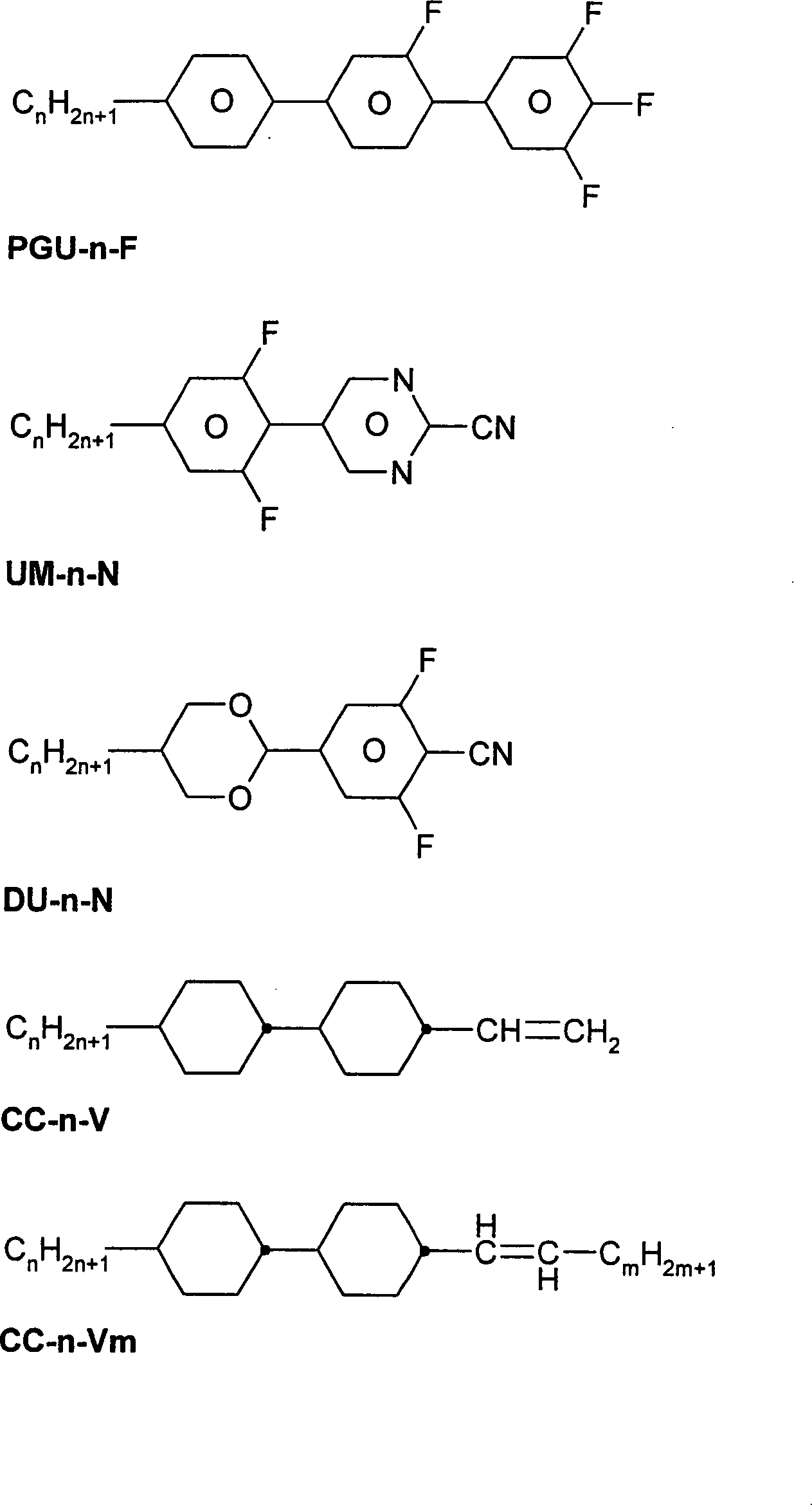
Die mesogenen Medien gemäß der vorliegenden Anmeldung enthalten bevorzugt
- – vier oder mehr, bevorzugt sechs oder mehr, Verbindungen ausgewählt aus der Gruppe der Verbindungen der Tabellen A und B und/oder
- – fünf oder mehr Verbindungen ausgewählt aus der Gruppe der Verbindungen der Tabelle B und/oder
- – zwei oder mehr Verbindungen ausgewählt aus der Gruppe der Verbindungen der Tabelle A.
- - Four or more, preferably six or more, compounds selected from the group of compounds of Tables A and B and / or
- - Five or more compounds selected from the group of compounds in Table B and / or
- Two or more compounds selected from the group of compounds in Table A.
BeispieleExamples
Die im Folgenden beschriebenen Beispiele illustrieren die vorliegende Erfindung ohne sie in irgend einer Art zu beschränken. Ferner zeigen sie dem Fachmann welche Eigenschaften und insbesondere welche Eigenschaftskombinationen mit der vorliegenden Endung erreicht werden können.The examples described below illustrate the present invention without it in any Kind of restrict. Furthermore, they show the skilled person which properties and in particular which combinations of properties achieved with the present ending can be.
VergleichsbeispielComparative example
Die mesogene mit der folgenden Zusammensetzung
wurde hergestellt.
Diese Mischung hat die folgenden
Eigenschaften.
Diese Flüssigkristallmischung Patentanmeldung
Die verwendete Testzelle wies, wie in der Anmeldung 1 dargestellt, Elektroden auf nur einem der beiden Substrate auf. Eine elektrooptische Testzelle mit einem Lichtschaltelement enthaltend die Flüssigkristallmischung wurde hergestellt. Die Substrate bestanden aus Glas. Es wurden Substrate ohne Orientierungsschicht verwendet. Die Elektrodenstruktur bestand aus ineinander verzahnten kammförmigen Elektroden. Der Abstand der Elektroden betrug 20 μm und die Breite der Elektroden voneinander betrug 10 μm. Die Schichtdicke der Elektroden betrug 60 nm. Die Elektroden befanden sich alle in einer gemeinsamen Ebene. Die Schichtdicke des Steuermediums betrug 6,8 μm.The test cell used showed how shown in application 1, electrodes on only one of the two Substrates. An electro-optical test cell with a light switching element containing the liquid crystal mixture was produced. The substrates were made of glass. There were substrates used without orientation layer. The electrode structure existed from interdigitated comb-shaped Electrodes. The distance between the electrodes was 20 μm and The width of the electrodes from each other was 10 μm. The layer thickness of the electrodes was 60 nm. The electrodes were all in one Level. The layer thickness of the control medium was 6.8 μm.
Es wurde ein erster Polarisator vor und als Analysator ein zweiter Polarisator hinter der Zelle benutzt. Die Absorptionsachsen der beiden Polarisatoren bildeten einen Winkel von 90° zueinander. Der Winkel zwischen der Achse der maximalen Absorption der Polarisatoren und der Komponente des elektrischen Felds in der Ebene der Anzeige betrug jeweils 45°. Die Spannungs-Transmissions-Kennlinie wurde mit einem elektrooptischen Messplatz DMS 703 der Firma Autronic-Melchers, Karlsruhe, Deutschland bestimmt. Die Betriebstemperatur betrug 24,0°C. Bei senkrechter Beobachtung wurde eine Kurve erhalten wie sie für eine Zelle mit elektrisch kontrollierter Doppelbrechung (z. B. ECB) typisch ist. Der Wert der Schwellenspannung (V10) lag bei 40,5 V, der Wert der Mittgrauspannung (V50) bei 56 V und der Wert der Sättigungsspannung (V90) bei 65 V. Der maximale Kontrast wurde bei 73 V erreicht. Bei Spannungen von 80 V bzw. 90 V sank der relative Kontrast wieder auf 90 % bzw. 50 % ab. Diese Ergebnisse sind auch in der folgenden Tabelle zusammengestellt.A first polarizer was used in front and a second polarizer behind the cell as the analyzer. The absorption axes of the two polarizers formed an angle of 90 ° to one another. The angle between the axis of maximum absorption of the polarizers and the component of the electric field in the plane of the display was 45 ° in each case. The voltage transmission characteristic was determined with an electro-optical measuring station DMS 703 from Autronic-Melchers, Karlsruhe, Germany. The operating temperature was 24.0 ° C. When observed vertically, a curve was obtained which is typical for a cell with electrically controlled birefringence (e.g. ECB). The value of the threshold voltage (V 10 ) was 40.5 V, the value of the medium gray voltage (V 50 ) was 56 V and the value of the saturation voltage (V 90 ) was 65 V. The maximum contrast was reached at 73 V. At voltages of 80 V or 90 V, the relative contrast dropped again to 90% or 50%. These results are also summarized in the following table.
Tabelle
1: Charakteristische Spannungen 
Beispiel 1example 1
Die Mischung des Vergleichsbeispiels wurde in eine Testzelle gemäß der Lehre der vorliegenden Anmeldung gefüllt und ihre elektrooptischen Eigenschaften ebenfalls bei einer Temperatur von 24°C bestimmt. Die Testzelle hatte den selben Aufbau wie die im Vergleichsbeispiel verwendete, jedoch betrug hier der Abstand zwischen den Elektroden 10 μm und die Breite der Elektroden 5 μm.The mixture of the comparative example was placed in a test cell according to the teaching filled the present application and their electro-optical properties also at one temperature of 24 ° C certainly. The test cell had the same structure as that in the comparative example used, but here was the distance between the electrodes 10 μm and the width of the electrodes 5 μm.
Die so erhaltene Zelle erreichte bei einer Spannung von 26,5 V 10 relativen Kontrast, bei 38 V 50 % relativen Kontrast und bei 46 V 90 % relativen Kontrast. Der maximale Kontrast wurde bei 51 V erreicht. Bei Spannungen von 60 V sank der relative Kontrast wieder auf 90 %. Diese Ergebnisse sind zum Vergleich mit denen des Vergleichsbeispiels in Tabelle 1 enthalten.The cell thus obtained reached at a voltage of 26.5 V 10 relative contrast, at 38 V 50 % relative contrast and at 46 V 90% relative contrast. The maximum Contrast was achieved at 51 V. At voltages of 60 V, the relative contrast back to 90%. These results are for comparison with those of the comparative example in Table 1.
Wie man aus dieser Tabelle ersehen kann, sind alle charakteristischen Spannungen des Flüssigkristallschaltelements des Beispiels 1 signifikant niedriger als die des Vergleichsbeispiels. Die Erniedrigung liegt im Durchschnitt für die ersten vier Werte bei etwa 31 %.As you can see from this table can, are all characteristic voltages of the liquid crystal switching element Example 1 significantly lower than that of the comparative example. The degradation is on average for the first four values about 31%.
Beispiel 2Example 2
Die im Vergleichsbeispiel und im
Beispiel 1 verwendete Mischung wurde in eine Testzelle gemäß einer anderen
Ausführungsform
der Lehre der vorliegenden Anmeldung gefüllt und ihre elektrooptischen
Eigenschaften ebenfalls bei einer Temperatur von 24 C bestimmt.
Die Testzelle hatte einen Aufbau gemäß
Die so erhaltene Zelle erreichte bei einer Spannung von 25 V 10 % relativen Kontrast, bei 33,5 V 50 % relativen Kontrast und bei 41 V 90 relativen Kontrast. Der maximale Kontrast wurde bei 45 V erreicht. Diese Ergebnisse sind ebenfalls in Tabelle 1 enthalten.The cell thus obtained reached at a voltage of 25 V 10% relative contrast, at 33.5 V 50% relative contrast and at 41 V 90 relative contrast. The maximum contrast was achieved at 45 V. These results are also included in Table 1.
Wie man hier sehen kann, sind alle charakteristischen Spannungen des Flüssigkristallschaltelements des Beispiels 2 noch einmal signifikant niedriger als die des Beispiels 1. Die Erniedrigung der entsprechenden Werte im Vergleich zu denen des Vergleichsbeispiels liegt hier im Durchschnitt bei etwa 38 %.As you can see here, everyone is characteristic voltages of the liquid crystal switching element of the Example 2 again significantly lower than that of the example 1. The lowering of the corresponding values compared to those of the comparative example here is on average around 38%.
Beispiel 3Example 3
Die im Vergleichsbeispiel und in den vorigen Beispielen 1 und 2 verwendete Mischung wurde in eine Testzelle gemäß noch einer weiteren Ausführungsform nach der Lehre der vorliegenden Anmeldung gefüllt und ihre elektrooptischen Eigenschaften ebenfalls bei einer Temperatur von 24 C bestimmt.The in the comparative example and in The mixture used in previous Examples 1 and 2 was placed in a test cell according to another another embodiment filled according to the teaching of the present application and its electro-optical Properties also determined at a temperature of 24 C.
Die Testzelle hatte Elektrodenpaaren
auf den Innenseiten beider Substrate wie in
Die so erhaltene Zelle erreichte bei einer Spannung von 21 V 10 relativen Kontrast, bei 29 V 50 % relativen Kontrast und bei 35 V 90 relativen Kontrast. Der maximale Kontrast wurde bei 37,5 V erreicht. Bei Spannungen von 41 V bzw. 47 V sank der relative Kontrast wieder auf 90 % bzw. 50 % ab. Diese Ergebnisse sind ebenfalls in Tabelle 1 enthalten.The cell thus obtained reached at a voltage of 21 V 10 relative contrast, at 29 V 50% relative contrast and at 35 V 90 relative contrast. The maximum Contrast was reached at 37.5 V. At voltages of 41 V or 47 V, the relative contrast dropped back to 90% and 50%, respectively. This Results are also shown in Table 1.
Wie man aus dieser Tabelle ersehen kann, sind alle charakteristischen Spannungen des Flüssigkristallschaltelement des Beispiels 2 erneut erniedrigt worden. Die Erniedrigung der entsprechenden Werte im Vergleich zu denen des Vergleichsbeispiels liegt hier im Durchschnitt bei etwa 48 %, somit sind die Werte nur etwa halb so groß wie die des Vergleichsbeispiels.As you can see from this table can, are all characteristic voltages of the liquid crystal switching element of Example 2 have been lowered again. The humiliation of the corresponding Values compared to those of the comparative example are in here Average at about 48%, so the values are only about half that as big as that of the comparative example.
Beispiel 4Example 4
Die Flüssigkristallmischung mit der
folgenden Zusammensetzung wurde hergestellt.
Diese Mischung hat die folgenden
Eigenschaften.
Wie bei Beispiel 3 wird eine elektro-optische Anzeige realisiert und deren Kennline vermessen. Die Temperatur beträgt 24,0°C. Der Wert der Schwellenspannung (V10) liegt bei 22 V, der Wert der Mittgrauspannung (V50) bei 35,5 V und der Wert der Sättigungsspannung (V90) bei 44,5 V.As in example 3, an electro-optical display is implemented and its characteristic is measured. The temperature is 24.0 ° C. The value of the threshold voltage (V 10 ) is 22 V, the value of the medium gray voltage (V 50 ) is 35.5 V and the value of the saturation voltage (V 90 ) is 44.5 V.
Beispiel 5Example 5
Die Flüssigkristallmischung mit der
folgenden Zusammensetzung wurde hergestellt.
Diese Mischung hat die folgenden
Eigenschaften.
Wie bei Beispiel 3 wird eine elektro-optische Anzeige realisiert und deren Kennline vermessen. Die Temperatur beträgt 26,5°C. Die Kennlinie beginnt bei niedriger Spannung mit einer relativen Intensität von 0% und steigt mit steigender Spannung an. Der Wert der Schwellenspannung (V10) liegt bei 18 V, der Wert der Mittgrauspannung (V5 0) bei 28 V und der Wert der Sättigungsspannung (V9 0) bei 34 V. Bei einer Spannung von 37 V wird das Maximum der Intensität erreicht.As in example 3, an electro-optical display is implemented and its characteristic is measured. The temperature is 26.5 ° C. The characteristic curve begins at a low voltage with a relative intensity of 0% and increases with increasing voltage. The value of the threshold voltage (V 10 ) is 18 V, the value of the medium gray voltage (V 5 0 ) is 28 V and the value of the saturation voltage (V 9 0 ) is 34 V. At a voltage of 37 V the maximum of the intensity reached.
Beispiel 6Example 6
Die Flüssigkristallmischung mit der
folgenden Zusammensetzung wurde hergestellt.
Diese Mischung hat die folgenden
Eigenschaften.
Wie bei Beispiel 3 wird eine elektro-optische Anzeige realisiert und deren Kennline vermessen. Die Temperatur bei der die Messungen durchgeführt wurden beträgt 23,1 °C.As in Example 3, an electro-optical Realized the display and measured its characteristic. The temperature at which the measurements were made were amounts 23.1 ° C.
Der Wert der Schwellenspannung (V10) liegt bei 36,5 V, der Wert der Mittgrauspannung (V50) bei 28 V und der Wert der Sättigungsspannung (V9 0) bei 31,5 V. Das Maximum des relativen Kontrasts liegt bei 34 V.The value of the threshold voltage (V 10 ) is 36.5 V, the value of the mid-gray voltage (V 50 ) is 28 V and the value of the saturation voltage (V 9 0 ) is 31.5 V. The maximum of the relative contrast is 34 V.
Beispiel 7Example 7
Die Flüssigkristallmischung mit der
folgenden Zusammensetzung wurde hergestellt.
Diese Mischung hat die folgenden
Eigenschaften.
Beispiel 8Example 8
Die Flüssigkristallmischung mit der
folgenden Zusammensetzung wurde hergestellt.
Diese Mischung hat die folgenden
Eigenschaften.
Beispiel 9Example 9
Die Flüssigkristallmischung mit der
folgenden Zusammensetzung wurde hergestellt.
Beispiel 10Example 10
Die Flüssigkristallmischung mit der
folgenden Zusammensetzung wurde hergestellt.
Diese Mischung hat die folgenden
Eigenschaften.
Beispiel 11Example 11
Die Flüssigkristallmischung mit der
folgenden Zusammensetzung wurde hergestellt.
Diese Mischung hat die folgenden
Eigenschaften.
Beispiel 12Example 12
Die Flüssigkristallmischung mit der
folgenden Zusammensetzung wurde hergestellt.
Diese Mischung hat die folgenden
Eigenschaften.
Δε (20 °C, 1 kHz) > 0 This mixture has the following properties.
Δε (20 ° C, 1 kHz)> 0
Beispiel 13Example 13
Die Flüssigkristallmischung mit der
folgenden Zusammensetzung wurde hergestellt.
Diese Mischung hat die folgenden
Eigenschaften.
Beispiel 14Example 14
Die Flüssigkristallmischung mit der
folgenden Zusammensetzung wurde hergestellt.
Diese Mischung hat die folgenden
Eigenschaften.
Beispiel 15Example 15
Die Flüssigkristallmischung mit der
folgenden Zusammensetzung wurde hergestellt.
Diese Mischung hat die folgenden
Eigenschaften.
Beispiel 16Example 16
Die Flüssigkristallmischung mit der
folgenden Zusammensetzung wurde hergestellt.
Diese Mischung hat die folgenden
Eigenschaften.
Beispiel 17Example 17
Die Flüssigkristallmischung mit der
folgenden Zusammensetzung wurde hergestellt.
Diese Mischung hat die folgenden
Eigenschaften.
Δε (20 °C, 1 kHz) < 0 This mixture has the following properties.
Δε (20 ° C, 1 kHz) <0
Beispiel 18Example 18
Die Flüssigkristallmischung mit der
folgenden Zusammensetzung wurde hergestellt.
Diese Mischung hat die folgenden
Eigenschaften.
Δε (20 °C, 1 kHz) < 0 This mixture has the following properties.
Δε (20 ° C, 1 kHz) <0
Beispiel 19Example 19
Die Flüssigkristallmischung mit der
folgenden Zusammensetzung wurde hergestellt.
Diese Mischung hat die folgenden
Eigenschaften.
Beispiel 20Example 20
Die Flüssigkristallmischung mit der
folgenden Zusammensetzung wurde hergestellt.
Diese Mischung hat die folgenden
Eigenschaften.
Beispiel 21Example 21
Die Flüssigkristallmischung mit der
folgenden Zusammensetzung wurde hergestellt.
Diese Mischung hat die folgenden
Eigenschaften.
Beispiel 22Example 22
Die Flüssigkristallmischung mit der
folgenden Zusammensetzung wurde hergestellt.
Diese Mischung hat die folgenden
Eigenschaften.
Beispiel 23Example 23
Die Flüssigkristallmischung mit der
folgenden Zusammensetzung wurde hergestellt.
Diese Mischung hat die folgenden
Eigenschaften.
Beispiel 24 Example 24
Die Flüssigkristallmischung mit der
folgenden Zusammensetzung wurde hergestellt.
Diese Mischung hat die folgenden
Eigenschaften.
Die Mischungen der Beispiele 4 bis 24 werden in Testzellen gemäß der Lehre gefüllt, wie in den Beispielen 1 bis 3 beschrieben. Die resultierenden Lichtsteuerelemente haben ähnlich gute Eigenschaften wie die in diesen drei Beispielen beschriebenen Lichtsteuerelemente.The mixtures of Examples 4 to 24 are in test cells according to the teaching filled, as described in Examples 1 to 3. The resulting light controls have similar good properties like those described in these three examples Light controls.
Beschreibung der Abbildungendescription of the pictures
Bei der
Bei der
Bei der
Bei der
Bei der
Bei der
Bei der
Bei der
Bei der
- 1 : 1 :
- Oberfläche des ersten Substrats,Surface of the first substrate,
- 1 ' :1 ':
- Oberfläche des 2. Substrats,Surface of the 2. substrate,
- 2 :2 :
- Steuerschicht,Control layer,
- 3 bis 3''': 3 to 3''':
- Erste bis vierte leitfähige Schicht der Elektrodenstruktur, die mit dem 1. Potential beaufschlagt werden kann,First to fourth conductive Layer of the electrode structure to which the 1st potential is applied can
- 4 bis 4''': 4 to 4''':
- Erste bis vierte leitfähige Schicht der Elektrodenstruktur, die mit dem 2. Potential beaufschlagt werden kann,First to fourth conductive Layer of the electrode structure to which the 2nd potential is applied can
- 5 bis 5'''': 5 until 5'''':
- Erste bis fünfte feste, isolierende Schicht der Elektrodenstruktur, die leitfähigen Schichten der Elektrodenstruktur, die mit dem 1. Potential beaufschlagt werden können, trennt,First to fifth solid, insulating layer of the electrode structure, the conductive layers the electrode structure to which the 1st potential is applied can, separates,
- 6 bis 6"": 6 until 6"":
- Erste bis fünfte feste, isolierende Schicht der Elektrodenstruktur, die leitfähigen Schichten der Elektrodenstruktur, die mit dem 2. Potential beaufschlagt werden können, trennt,First to fifth solid, insulating layer of the electrode structure, the conductive layers the electrode structure to which the 2nd potential is applied can, separates,
- Vop : Vop :
- Spannungs-, Ladungs- bzw. Stromquellevoltage, Charge or current source
Die von Vop ausgehenden Linien veranschaulichen die welche leitfähigen Schichten der Elektrodenstruktur mit dem gleichen Potential beaufschlagt werden.Illustrate the lines from Vop which are conductive Layers of the electrode structure are exposed to the same potential become.
Claims (14)
Priority Applications (6)
| Application Number | Priority Date | Filing Date | Title |
|---|---|---|---|
| DE10241301A DE10241301A1 (en) | 2002-09-04 | 2002-09-04 | Electrooptic light control element and display and medium for television and computer screens has temperature driven control mechanism |
| PCT/EP2003/009402 WO2004029697A1 (en) | 2002-09-04 | 2003-08-25 | Electro-optic light control element comprising a medium with an optical isotropic phase and electro-optic displays equipped with said element |
| DE10392930.4T DE10392930B4 (en) | 2002-09-04 | 2003-08-25 | Electro-optical light control element with medium with optically isotropic phase and thus equipped electro-optical displays |
| AU2003264099A AU2003264099A1 (en) | 2002-09-04 | 2003-08-25 | Electro-optic light control element comprising a medium with an optical isotropic phase and electro-optic displays equipped with said element |
| JP2004538836A JP5106753B2 (en) | 2002-09-04 | 2003-08-25 | ELECTRO-OPTICAL LIGHT MODULATION ELEMENT CONTAINING MEDIUM HAVING OPTICALLY ISOTOPE PHASE, AND ELECTRO-OPTICAL DISPLAY HAVING SAME |
| TW092123574A TW200408865A (en) | 2002-09-04 | 2003-08-27 | Electro-optical light modulation element, display and medium |
Applications Claiming Priority (1)
| Application Number | Priority Date | Filing Date | Title |
|---|---|---|---|
| DE10241301A DE10241301A1 (en) | 2002-09-04 | 2002-09-04 | Electrooptic light control element and display and medium for television and computer screens has temperature driven control mechanism |
Publications (1)
| Publication Number | Publication Date |
|---|---|
| DE10241301A1 true DE10241301A1 (en) | 2004-03-18 |
Family
ID=31724428
Family Applications (2)
| Application Number | Title | Priority Date | Filing Date |
|---|---|---|---|
| DE10241301A Withdrawn DE10241301A1 (en) | 2002-09-04 | 2002-09-04 | Electrooptic light control element and display and medium for television and computer screens has temperature driven control mechanism |
| DE10392930.4T Expired - Fee Related DE10392930B4 (en) | 2002-09-04 | 2003-08-25 | Electro-optical light control element with medium with optically isotropic phase and thus equipped electro-optical displays |
Family Applications After (1)
| Application Number | Title | Priority Date | Filing Date |
|---|---|---|---|
| DE10392930.4T Expired - Fee Related DE10392930B4 (en) | 2002-09-04 | 2003-08-25 | Electro-optical light control element with medium with optically isotropic phase and thus equipped electro-optical displays |
Country Status (5)
| Country | Link |
|---|---|
| JP (1) | JP5106753B2 (en) |
| AU (1) | AU2003264099A1 (en) |
| DE (2) | DE10241301A1 (en) |
| TW (1) | TW200408865A (en) |
| WO (1) | WO2004029697A1 (en) |
Cited By (18)
| Publication number | Priority date | Publication date | Assignee | Title |
|---|---|---|---|---|
| WO2005019381A1 (en) * | 2003-08-25 | 2005-03-03 | Merck Patent Gmbh | Liquid crystalline medium |
| WO2005095544A1 (en) * | 2004-03-25 | 2005-10-13 | Merck Patent Gmbh | Liquid crystal compounds, liquid crystal medium and liquid crystal display |
| WO2006015683A1 (en) * | 2004-08-10 | 2006-02-16 | Merck Patent Gmbh | Liquid crystal compounds, liquid crystal medium and liquid crystal display |
| DE102011011836A1 (en) | 2010-03-09 | 2011-09-15 | Merck Patent Gmbh | Polymerizable compounds and their use in liquid crystal media and liquid crystal displays |
| EP2380945A1 (en) | 2010-04-26 | 2011-10-26 | Merck Patent GmbH | Polymerisable compounds and use of same in liquid crystal media and liquid crystal displays |
| DE102012009631A1 (en) | 2011-05-27 | 2012-11-29 | Merck Patent Gmbh | Polymerizable compounds and their use in liquid crystal media and liquid crystal displays |
| WO2012163470A1 (en) | 2011-06-01 | 2012-12-06 | Merck Patent Gmbh | Liquid crystal medium and liquid crystal display |
| WO2013017197A1 (en) | 2011-08-01 | 2013-02-07 | Merck Patent Gmbh | Liquid crystal medium and liquid crystal display |
| EP2568032A2 (en) | 2011-09-06 | 2013-03-13 | Merck Patent GmbH | Liquid crystal medium and liquid crystal display |
| WO2013034219A1 (en) | 2011-09-06 | 2013-03-14 | Merck Patent Gmbh | Liquid crystal medium and liquid crystal display |
| US8420235B2 (en) | 2009-06-04 | 2013-04-16 | Nitto Denko Corporation | Emissive diaryl acetylenes |
| WO2013156113A1 (en) | 2012-04-20 | 2013-10-24 | Merck Patent Gmbh | Liquid crystal medium and liquid crystal display |
| EP2708587A1 (en) | 2012-09-18 | 2014-03-19 | Merck Patent GmbH | Liquid crystal medium and liquid crystal display |
| WO2014053204A1 (en) | 2012-10-02 | 2014-04-10 | Merck Patent Gmbh | Liquid crystal medium and liquid crystal display |
| WO2014169985A1 (en) | 2013-04-19 | 2014-10-23 | Merck Patent Gmbh | Mesogenic compound, liquid crystal medium and liquid crystal display |
| WO2015101405A1 (en) | 2013-12-30 | 2015-07-09 | Merck Patent Gmbh | Liquid crystal medium and liquid crystal display |
| EP3124573A1 (en) | 2015-07-31 | 2017-02-01 | Merck Patent GmbH | Liquid crystal medium and liquid crystal display |
| EP2886627B1 (en) * | 2013-12-19 | 2019-05-15 | Merck Patent GmbH | Liquid crystalline medium |
Families Citing this family (19)
| Publication number | Priority date | Publication date | Assignee | Title |
|---|---|---|---|---|
| JP4138759B2 (en) | 2005-02-03 | 2008-08-27 | セイコーエプソン株式会社 | Liquid crystal display device and electronic device |
| JP5577566B2 (en) | 2007-08-31 | 2014-08-27 | Jnc株式会社 | Liquid crystal composition and liquid crystal element |
| US8339556B2 (en) | 2008-03-03 | 2012-12-25 | Hitachi Displays, Ltd. | Electro-optical device and display device with interdigital electrode portions on at least first and second substrates which are non-overlapping in a direction normal to the substrates |
| JP5236529B2 (en) * | 2008-03-03 | 2013-07-17 | 株式会社ジャパンディスプレイイースト | ELECTRO-OPTICAL ELEMENT AND DISPLAY DEVICE |
| US8496850B2 (en) * | 2008-09-01 | 2013-07-30 | Jnc Corporation | Liquid crystal composition and liquid crystal display device |
| JP5623433B2 (en) | 2009-02-19 | 2014-11-12 | メルク パテント ゲゼルシャフト ミット ベシュレンクテル ハフツングMerck Patent Gesellschaft mit beschraenkter Haftung | Thiophene derivative and liquid crystal medium containing the same |
| JP4550152B2 (en) * | 2009-07-13 | 2010-09-22 | シャープ株式会社 | Display element |
| JP5765227B2 (en) | 2009-10-01 | 2015-08-19 | Jnc株式会社 | Liquid crystalline compound having negative dielectric anisotropy, liquid crystal composition using the same, and liquid crystal display device |
| TWI427379B (en) * | 2010-10-26 | 2014-02-21 | Au Optronics Corp | Liquid crystal display panel |
| CN102062978A (en) * | 2010-11-10 | 2011-05-18 | 友达光电股份有限公司 | Liquid crystal display panel |
| CN104854217B (en) | 2012-12-17 | 2017-06-23 | 捷恩智株式会社 | Liquid-crystal composition, mixture, composite, liquid crystal cell and chipal compounds |
| WO2014094973A1 (en) | 2012-12-21 | 2014-06-26 | Merck Patent Gmbh | Liquid-crystalline media, components for high-frequency technology, and mesogenic compounds |
| CN108239538B (en) * | 2016-12-23 | 2022-02-08 | 江苏和成显示科技有限公司 | Liquid crystal composition with negative dielectric anisotropy and application thereof |
| DE102017000406A1 (en) * | 2017-01-18 | 2018-07-19 | Stephanie Faustig | Electrically controllable optical element, in particular thin-layer cell and method for its production |
| GB2575579B (en) | 2017-03-21 | 2022-08-10 | Merck Patent Gmbh | Light modulation element |
| GB2575591B (en) | 2017-03-28 | 2022-10-19 | Merck Patent Gmbh | Liquid crystal device |
| US11124705B2 (en) | 2017-04-20 | 2021-09-21 | Merck Patent Gmbh | Light modulation element |
| DE112018005653T5 (en) | 2017-11-21 | 2020-07-02 | Merck Patent Gmbh | Liquid crystal medium and light modulation element |
| CN110109295B (en) * | 2019-04-08 | 2022-01-04 | Tcl华星光电技术有限公司 | Blue phase liquid crystal display panel |
Family Cites Families (10)
| Publication number | Priority date | Publication date | Assignee | Title |
|---|---|---|---|---|
| CH540500A (en) * | 1971-07-16 | 1973-08-15 | Hoffmann La Roche | Electro-optical light control cell |
| EP0588568B1 (en) * | 1992-09-18 | 2002-12-18 | Hitachi, Ltd. | A liquid crystal display device |
| JPH06250210A (en) * | 1993-02-23 | 1994-09-09 | Hitachi Ltd | Liquid crystal display device and its production |
| JP3238230B2 (en) * | 1993-02-26 | 2001-12-10 | 株式会社東芝 | Liquid crystal display |
| JPH09185080A (en) * | 1995-12-28 | 1997-07-15 | Semiconductor Energy Lab Co Ltd | Liquid crystal electro-optical device |
| JP3712772B2 (en) * | 1996-01-29 | 2005-11-02 | 株式会社半導体エネルギー研究所 | Liquid crystal electro-optical device |
| JP3174497B2 (en) * | 1996-03-19 | 2001-06-11 | シャープ株式会社 | Liquid crystal display |
| JP3504159B2 (en) * | 1997-10-16 | 2004-03-08 | 株式会社東芝 | Liquid crystal optical switch element |
| JP2001249363A (en) * | 2000-03-06 | 2001-09-14 | Matsushita Electric Ind Co Ltd | Display device |
| US7701628B2 (en) * | 2001-05-16 | 2010-04-20 | Merck Patent Gmbh | Electro-optic light control element, display and medium |
-
2002
- 2002-09-04 DE DE10241301A patent/DE10241301A1/en not_active Withdrawn
-
2003
- 2003-08-25 AU AU2003264099A patent/AU2003264099A1/en not_active Abandoned
- 2003-08-25 JP JP2004538836A patent/JP5106753B2/en not_active Expired - Fee Related
- 2003-08-25 WO PCT/EP2003/009402 patent/WO2004029697A1/en active Application Filing
- 2003-08-25 DE DE10392930.4T patent/DE10392930B4/en not_active Expired - Fee Related
- 2003-08-27 TW TW092123574A patent/TW200408865A/en unknown
Cited By (23)
| Publication number | Priority date | Publication date | Assignee | Title |
|---|---|---|---|---|
| US7419706B2 (en) | 2003-08-25 | 2008-09-02 | Merck Patent Gesellschaft Mit Beschrankter Haftung | Liquid crystalline medium |
| WO2005019381A1 (en) * | 2003-08-25 | 2005-03-03 | Merck Patent Gmbh | Liquid crystalline medium |
| WO2005095544A1 (en) * | 2004-03-25 | 2005-10-13 | Merck Patent Gmbh | Liquid crystal compounds, liquid crystal medium and liquid crystal display |
| DE112005000732T5 (en) | 2004-03-25 | 2008-09-04 | Merck Patent Gmbh | Liquid crystal compounds, liquid crystal medium and liquid crystal display |
| WO2006015683A1 (en) * | 2004-08-10 | 2006-02-16 | Merck Patent Gmbh | Liquid crystal compounds, liquid crystal medium and liquid crystal display |
| US8420235B2 (en) | 2009-06-04 | 2013-04-16 | Nitto Denko Corporation | Emissive diaryl acetylenes |
| DE102011011836A1 (en) | 2010-03-09 | 2011-09-15 | Merck Patent Gmbh | Polymerizable compounds and their use in liquid crystal media and liquid crystal displays |
| WO2011110287A1 (en) | 2010-03-09 | 2011-09-15 | Merck Patent Gmbh | Polymerizable compounds and their use in liquid-crystal media and liquid-crystal displays |
| EP2380945A1 (en) | 2010-04-26 | 2011-10-26 | Merck Patent GmbH | Polymerisable compounds and use of same in liquid crystal media and liquid crystal displays |
| DE102011015546A1 (en) | 2010-04-26 | 2012-01-26 | Merck Patent Gmbh | Polymerizable compounds and their use in liquid crystal media and liquid crystal displays |
| WO2012163478A1 (en) | 2011-05-27 | 2012-12-06 | Merck Patent Gmbh | Polymerizable compounds and their use in liquid crystal media and liquid crystal displays |
| DE102012009631A1 (en) | 2011-05-27 | 2012-11-29 | Merck Patent Gmbh | Polymerizable compounds and their use in liquid crystal media and liquid crystal displays |
| WO2012163470A1 (en) | 2011-06-01 | 2012-12-06 | Merck Patent Gmbh | Liquid crystal medium and liquid crystal display |
| WO2013017197A1 (en) | 2011-08-01 | 2013-02-07 | Merck Patent Gmbh | Liquid crystal medium and liquid crystal display |
| EP2568032A2 (en) | 2011-09-06 | 2013-03-13 | Merck Patent GmbH | Liquid crystal medium and liquid crystal display |
| WO2013034219A1 (en) | 2011-09-06 | 2013-03-14 | Merck Patent Gmbh | Liquid crystal medium and liquid crystal display |
| WO2013156113A1 (en) | 2012-04-20 | 2013-10-24 | Merck Patent Gmbh | Liquid crystal medium and liquid crystal display |
| EP2708587A1 (en) | 2012-09-18 | 2014-03-19 | Merck Patent GmbH | Liquid crystal medium and liquid crystal display |
| WO2014053204A1 (en) | 2012-10-02 | 2014-04-10 | Merck Patent Gmbh | Liquid crystal medium and liquid crystal display |
| WO2014169985A1 (en) | 2013-04-19 | 2014-10-23 | Merck Patent Gmbh | Mesogenic compound, liquid crystal medium and liquid crystal display |
| EP2886627B1 (en) * | 2013-12-19 | 2019-05-15 | Merck Patent GmbH | Liquid crystalline medium |
| WO2015101405A1 (en) | 2013-12-30 | 2015-07-09 | Merck Patent Gmbh | Liquid crystal medium and liquid crystal display |
| EP3124573A1 (en) | 2015-07-31 | 2017-02-01 | Merck Patent GmbH | Liquid crystal medium and liquid crystal display |
Also Published As
| Publication number | Publication date |
|---|---|
| JP2005537520A (en) | 2005-12-08 |
| JP5106753B2 (en) | 2012-12-26 |
| DE10392930D2 (en) | 2005-07-07 |
| DE10392930B4 (en) | 2015-09-03 |
| TW200408865A (en) | 2004-06-01 |
| AU2003264099A1 (en) | 2004-04-19 |
| WO2004029697A1 (en) | 2004-04-08 |
Similar Documents
| Publication | Publication Date | Title |
|---|---|---|
| DE10392930B4 (en) | Electro-optical light control element with medium with optically isotropic phase and thus equipped electro-optical displays | |
| EP1560895B1 (en) | Electrooptic light control element, electrooptic display and control medium | |
| DE10217273A1 (en) | Electro-optical light control element, for use in display systems e.g. television and computer screens, is operated at a temperature at which the mesogenic control medium is in the isotropic phase | |
| DE102008039750B4 (en) | Electro-optical light control element, electro-optical display and electro-optical display system and uses thereof | |
| EP1561150A1 (en) | Electrooptical light modulating element, electrooptical display and modulating medium | |
| DE4042747B4 (en) | Electro-optical liquid crystal switching element | |
| DE4000451B4 (en) | Electro-optical liquid crystal switching element | |
| DE69333414T2 (en) | Liquid crystal device having a plurality of domains with different threshold voltages for switching liquid crystals | |
| DE10253606A1 (en) | Electro-optical light control element used in an electro-optical display system comprises one or more substrate, an electrode arrangement, one or more elements for polarizing light, and a control medium | |
| DE2418364A1 (en) | NEMATIC LIQUID CRYSTAL SYSTEM FOR ELECTROOPTIC DISPLAY ELEMENTS | |
| DE10313979A1 (en) | Electrooptical light modulating element for data display in electrooptical, video or digital system, e.g. active matrix display, television screen and computer monitor, uses mesogenic modulating medium with blue phase | |
| EP1558965B1 (en) | Electro-optical light control element and display having a control medium with an optically isotropic phase | |
| EP0376029B1 (en) | Black/white liquid-crystal display | |
| DE10135247B4 (en) | Liquid-crystalline medium and its use in liquid-crystal display | |
| DE3138518C1 (en) | Field effect liquid crystal cell | |
| EP1208182B1 (en) | Smectic liquid crystal high-contrast control or display device | |
| DE4212744C2 (en) | TN cell with d. DELTAn between 0.15 and 0.70 mum | |
| DE4422218A1 (en) | Dye-doped TN-LCD with retardation films for a wide viewing angle | |
| DE60115015T2 (en) | Liquid crystal cell system and method for improving a liquid crystal cell system | |
| DE10336783A1 (en) | Electrooptical light modulating element for data display in electrooptical, video or digital system, e.g. active matrix display, television screen and computer monitor, uses mesogenic modulating medium with blue phase | |
| DE2705399A1 (en) | LIQUID CRYSTAL INDICATOR WITH WOUNDED NEMATIC LIQUID CRYSTAL AND PROCEDURE TO REMOVE DISCLINATIONS IN SUCH ADVERTISEMENTS | |
| DE112018005653T5 (en) | Liquid crystal medium and light modulation element | |
| DE19911923A1 (en) | Ferroelectric liquid crystal display with active matrix elements and asymmetrical orientation layers | |
| DE4340271A1 (en) | Liq. crystal display with contrast independent of viewing angle | |
| DE19934124A1 (en) | Manufacturing LCDs involves applying electric field during display cell filling process, nematic liquid crystal medium in display cell is homeotropically oriented when in rest state |
Legal Events
| Date | Code | Title | Description |
|---|---|---|---|
| 8181 | Inventor (new situation) |
Inventor name: CZANTA, MARKUS, DR., 55116 MAINZ, DE Inventor name: HECKMEIER, MICHAEL, DR., 69502 HEMSBACH, DE Inventor name: GöTZ, ACHIM, 64665 ALSBACH-HäHNLEIN, DE Inventor name: PLACH, HERBERT, DR., 64291 DARMSTADT, DE |
|
| 8143 | Withdrawn due to claiming internal priority |