DE102012222927A1 - Organic layer deposition apparatus, method of manufacturing organic light emitting display devices using the same and organic light emitting display devices manufactured using the method - Google Patents
Organic layer deposition apparatus, method of manufacturing organic light emitting display devices using the same and organic light emitting display devices manufactured using the method Download PDFInfo
- Publication number
- DE102012222927A1 DE102012222927A1 DE102012222927A DE102012222927A DE102012222927A1 DE 102012222927 A1 DE102012222927 A1 DE 102012222927A1 DE 102012222927 A DE102012222927 A DE 102012222927A DE 102012222927 A DE102012222927 A DE 102012222927A DE 102012222927 A1 DE102012222927 A1 DE 102012222927A1
- Authority
- DE
- Germany
- Prior art keywords
- substrate
- deposition
- unit
- organic layer
- organic layers
- Prior art date
- Legal status (The legal status is an assumption and is not a legal conclusion. Google has not performed a legal analysis and makes no representation as to the accuracy of the status listed.)
- Pending
Links
Images


Classifications
-
- H—ELECTRICITY
- H05—ELECTRIC TECHNIQUES NOT OTHERWISE PROVIDED FOR
- H05B—ELECTRIC HEATING; ELECTRIC LIGHT SOURCES NOT OTHERWISE PROVIDED FOR; CIRCUIT ARRANGEMENTS FOR ELECTRIC LIGHT SOURCES, IN GENERAL
- H05B33/00—Electroluminescent light sources
- H05B33/10—Apparatus or processes specially adapted to the manufacture of electroluminescent light sources
-
- C—CHEMISTRY; METALLURGY
- C23—COATING METALLIC MATERIAL; COATING MATERIAL WITH METALLIC MATERIAL; CHEMICAL SURFACE TREATMENT; DIFFUSION TREATMENT OF METALLIC MATERIAL; COATING BY VACUUM EVAPORATION, BY SPUTTERING, BY ION IMPLANTATION OR BY CHEMICAL VAPOUR DEPOSITION, IN GENERAL; INHIBITING CORROSION OF METALLIC MATERIAL OR INCRUSTATION IN GENERAL
- C23C—COATING METALLIC MATERIAL; COATING MATERIAL WITH METALLIC MATERIAL; SURFACE TREATMENT OF METALLIC MATERIAL BY DIFFUSION INTO THE SURFACE, BY CHEMICAL CONVERSION OR SUBSTITUTION; COATING BY VACUUM EVAPORATION, BY SPUTTERING, BY ION IMPLANTATION OR BY CHEMICAL VAPOUR DEPOSITION, IN GENERAL
- C23C14/00—Coating by vacuum evaporation, by sputtering or by ion implantation of the coating forming material
- C23C14/06—Coating by vacuum evaporation, by sputtering or by ion implantation of the coating forming material characterised by the coating material
- C23C14/12—Organic material
-
- C—CHEMISTRY; METALLURGY
- C23—COATING METALLIC MATERIAL; COATING MATERIAL WITH METALLIC MATERIAL; CHEMICAL SURFACE TREATMENT; DIFFUSION TREATMENT OF METALLIC MATERIAL; COATING BY VACUUM EVAPORATION, BY SPUTTERING, BY ION IMPLANTATION OR BY CHEMICAL VAPOUR DEPOSITION, IN GENERAL; INHIBITING CORROSION OF METALLIC MATERIAL OR INCRUSTATION IN GENERAL
- C23C—COATING METALLIC MATERIAL; COATING MATERIAL WITH METALLIC MATERIAL; SURFACE TREATMENT OF METALLIC MATERIAL BY DIFFUSION INTO THE SURFACE, BY CHEMICAL CONVERSION OR SUBSTITUTION; COATING BY VACUUM EVAPORATION, BY SPUTTERING, BY ION IMPLANTATION OR BY CHEMICAL VAPOUR DEPOSITION, IN GENERAL
- C23C14/00—Coating by vacuum evaporation, by sputtering or by ion implantation of the coating forming material
- C23C14/22—Coating by vacuum evaporation, by sputtering or by ion implantation of the coating forming material characterised by the process of coating
- C23C14/50—Substrate holders
-
- H—ELECTRICITY
- H01—ELECTRIC ELEMENTS
- H01L—SEMICONDUCTOR DEVICES NOT COVERED BY CLASS H10
- H01L21/00—Processes or apparatus adapted for the manufacture or treatment of semiconductor or solid state devices or of parts thereof
- H01L21/67—Apparatus specially adapted for handling semiconductor or electric solid state devices during manufacture or treatment thereof; Apparatus specially adapted for handling wafers during manufacture or treatment of semiconductor or electric solid state devices or components ; Apparatus not specifically provided for elsewhere
- H01L21/67005—Apparatus not specifically provided for elsewhere
- H01L21/67011—Apparatus for manufacture or treatment
- H01L21/67155—Apparatus for manufacturing or treating in a plurality of work-stations
- H01L21/67161—Apparatus for manufacturing or treating in a plurality of work-stations characterized by the layout of the process chambers
- H01L21/67173—Apparatus for manufacturing or treating in a plurality of work-stations characterized by the layout of the process chambers in-line arrangement
-
- H—ELECTRICITY
- H01—ELECTRIC ELEMENTS
- H01L—SEMICONDUCTOR DEVICES NOT COVERED BY CLASS H10
- H01L21/00—Processes or apparatus adapted for the manufacture or treatment of semiconductor or solid state devices or of parts thereof
- H01L21/67—Apparatus specially adapted for handling semiconductor or electric solid state devices during manufacture or treatment thereof; Apparatus specially adapted for handling wafers during manufacture or treatment of semiconductor or electric solid state devices or components ; Apparatus not specifically provided for elsewhere
- H01L21/677—Apparatus specially adapted for handling semiconductor or electric solid state devices during manufacture or treatment thereof; Apparatus specially adapted for handling wafers during manufacture or treatment of semiconductor or electric solid state devices or components ; Apparatus not specifically provided for elsewhere for conveying, e.g. between different workstations
- H01L21/67703—Apparatus specially adapted for handling semiconductor or electric solid state devices during manufacture or treatment thereof; Apparatus specially adapted for handling wafers during manufacture or treatment of semiconductor or electric solid state devices or components ; Apparatus not specifically provided for elsewhere for conveying, e.g. between different workstations between different workstations
- H01L21/67709—Apparatus specially adapted for handling semiconductor or electric solid state devices during manufacture or treatment thereof; Apparatus specially adapted for handling wafers during manufacture or treatment of semiconductor or electric solid state devices or components ; Apparatus not specifically provided for elsewhere for conveying, e.g. between different workstations between different workstations using magnetic elements
-
- H—ELECTRICITY
- H01—ELECTRIC ELEMENTS
- H01L—SEMICONDUCTOR DEVICES NOT COVERED BY CLASS H10
- H01L21/00—Processes or apparatus adapted for the manufacture or treatment of semiconductor or solid state devices or of parts thereof
- H01L21/67—Apparatus specially adapted for handling semiconductor or electric solid state devices during manufacture or treatment thereof; Apparatus specially adapted for handling wafers during manufacture or treatment of semiconductor or electric solid state devices or components ; Apparatus not specifically provided for elsewhere
- H01L21/677—Apparatus specially adapted for handling semiconductor or electric solid state devices during manufacture or treatment thereof; Apparatus specially adapted for handling wafers during manufacture or treatment of semiconductor or electric solid state devices or components ; Apparatus not specifically provided for elsewhere for conveying, e.g. between different workstations
- H01L21/67739—Apparatus specially adapted for handling semiconductor or electric solid state devices during manufacture or treatment thereof; Apparatus specially adapted for handling wafers during manufacture or treatment of semiconductor or electric solid state devices or components ; Apparatus not specifically provided for elsewhere for conveying, e.g. between different workstations into and out of processing chamber
- H01L21/6776—Continuous loading and unloading into and out of a processing chamber, e.g. transporting belts within processing chambers
-
- H—ELECTRICITY
- H01—ELECTRIC ELEMENTS
- H01L—SEMICONDUCTOR DEVICES NOT COVERED BY CLASS H10
- H01L21/00—Processes or apparatus adapted for the manufacture or treatment of semiconductor or solid state devices or of parts thereof
- H01L21/67—Apparatus specially adapted for handling semiconductor or electric solid state devices during manufacture or treatment thereof; Apparatus specially adapted for handling wafers during manufacture or treatment of semiconductor or electric solid state devices or components ; Apparatus not specifically provided for elsewhere
- H01L21/683—Apparatus specially adapted for handling semiconductor or electric solid state devices during manufacture or treatment thereof; Apparatus specially adapted for handling wafers during manufacture or treatment of semiconductor or electric solid state devices or components ; Apparatus not specifically provided for elsewhere for supporting or gripping
- H01L21/6831—Apparatus specially adapted for handling semiconductor or electric solid state devices during manufacture or treatment thereof; Apparatus specially adapted for handling wafers during manufacture or treatment of semiconductor or electric solid state devices or components ; Apparatus not specifically provided for elsewhere for supporting or gripping using electrostatic chucks
-
- H—ELECTRICITY
- H10—SEMICONDUCTOR DEVICES; ELECTRIC SOLID-STATE DEVICES NOT OTHERWISE PROVIDED FOR
- H10K—ORGANIC ELECTRIC SOLID-STATE DEVICES
- H10K71/00—Manufacture or treatment specially adapted for the organic devices covered by this subclass
-
- H—ELECTRICITY
- H10—SEMICONDUCTOR DEVICES; ELECTRIC SOLID-STATE DEVICES NOT OTHERWISE PROVIDED FOR
- H10K—ORGANIC ELECTRIC SOLID-STATE DEVICES
- H10K19/00—Integrated devices, or assemblies of multiple devices, comprising at least one organic element specially adapted for rectifying, amplifying, oscillating or switching, covered by group H10K10/00
-
- H—ELECTRICITY
- H10—SEMICONDUCTOR DEVICES; ELECTRIC SOLID-STATE DEVICES NOT OTHERWISE PROVIDED FOR
- H10K—ORGANIC ELECTRIC SOLID-STATE DEVICES
- H10K59/00—Integrated devices, or assemblies of multiple devices, comprising at least one organic light-emitting element covered by group H10K50/00
- H10K59/10—OLED displays
- H10K59/12—Active-matrix OLED [AMOLED] displays
- H10K59/1201—Manufacture or treatment
-
- H—ELECTRICITY
- H10—SEMICONDUCTOR DEVICES; ELECTRIC SOLID-STATE DEVICES NOT OTHERWISE PROVIDED FOR
- H10K—ORGANIC ELECTRIC SOLID-STATE DEVICES
- H10K71/00—Manufacture or treatment specially adapted for the organic devices covered by this subclass
- H10K71/10—Deposition of organic active material
- H10K71/16—Deposition of organic active material using physical vapour deposition [PVD], e.g. vacuum deposition or sputtering
- H10K71/164—Deposition of organic active material using physical vapour deposition [PVD], e.g. vacuum deposition or sputtering using vacuum deposition
Abstract
Ein Gerät zur Abscheidung organischer Schichten (1), ein Verfahren zum Fertigen einer Vorrichtung mit organischer lichtemittierender Anzeige unter Verwendung desselben und ein unter Verwendung des Verfahrens gefertigte Vorrichtung mit organischer lichtemittierender Anzeige, und insbesondere ein Gerät zur Abscheidung organischer Schichten (1), das zur Verwendung in der Massenfertigung eines großen Substrats geeignet ist und eine hochauflösende Strukturierung ermöglicht, ein Verfahren zum Fertigen einer Vorrichtung mit organischer lichtemittierender Anzeige unter Verwendung desselben und eine unter Verwendung des Verfahrens gefertigte Vorrichtung mit organischer lichtemittierender Anzeige.An organic layer deposition apparatus (1), a method of fabricating an organic light emitting display device using the same, and an organic light emitting display device fabricated using the method, and more particularly to an organic layer deposition apparatus (1) useful in Is suitable for mass production of a large substrate and enables high resolution patterning, a method of fabricating an organic light emitting display device using the same, and an organic light emitting display device manufactured using the method.
Description
Hintergrundbackground
1. Gebiet1st area
Aspekte der vorliegenden Erfindung beziehen sich auf ein Gerät zur Abscheidung organischer Schichten, ein Verfahren zum Fertigen einer Vorrichtung mit organischer lichtemittierender Anzeige unter Verwendung desselben und eine unter Verwendung des Verfahrens gefertigte Vorrichtung mit organischer lichtemittierender Anzeige.Aspects of the present invention relate to an organic layer deposition apparatus, a method of fabricating an organic light emitting display device using the same, and an organic light emitting display device manufactured using the method.
2. Einschlägiger Stand der Technik2. Relevant prior art
Vorrichtungen mit organischer lichtemittierender Anzeige haben größere Betrachtungswinkel, bessere Kontrasteigenschaften und höhere Ansprechgeschwindigkeiten als andere Anzeigevorrichtungen und sind daher als Anzeigevorrichtung der nächsten Generation von Interesse.Organic light-emitting display devices have larger viewing angles, better contrast characteristics, and higher response speeds than other display devices, and are therefore of interest as the next generation display device.
Eine Vorrichtung mit organischer lichtemittierender Anzeige umfasst Zwischenschichten (umfassend eine Emissionsschicht), die zwischen einer ersten Elektrode und einer zweiten Elektrode angeordnet sind. Die Elektroden und die Zwischenschichten können unter Verwendung verschiedener Verfahren, darunter ein unabhängiges Abscheidungsverfahren, ausgebildet sein. Bei der Fertigung einer Vorrichtung mit organischer lichtemittierender Anzeige unter Verwendung des Abscheidungsverfahrens wird eine Feinmetallmaske (FMM) mit derselben Strukturierung wie der einer auszubildenden organischen Schicht so angeordnet, dass sie in engem Kontakt mit einem Substrat steht, auf dem die organische Schicht und dergleichen ausgebildet werden, und ein organisches Schichtmaterial wird auf der FMM abgeschieden, um die organische Schicht mit der gewünschten Strukturierung auszubilden.An organic light emitting display device includes intermediate layers (including an emission layer) disposed between a first electrode and a second electrode. The electrodes and the interlayers may be formed using various methods, including an independent deposition method. In fabricating an organic light emitting display device using the deposition method, a fine metal mask (FMM) having the same patterning as that of an organic layer to be formed is disposed so as to be in close contact with a substrate on which the organic layer and the like are formed and an organic layer material is deposited on the FMM to form the organic layer having the desired patterning.
Das Abscheidungsverfahren unter Verwendung einer solchen FMM bereitet allerdings bei der Fertigung größerer Vorrichtungen mit organischer lichtemittierender Anzeige unter Verwendung eines großen Mutterglases Schwierigkeiten. Wird beispielsweise eine solche große Maske verwendet, kann sich die Maske aufgrund der Eigengravitation krümmen und dadurch eine Strukturierung verzerren. Diese Mängel sind der aktuellen Entwicklung in Richtung hochauflösender Strukturierungen nicht zuträglich.However, the deposition method using such FMM is troublesome in manufacturing larger organic light emitting display devices using a large mother glass. For example, if such a large mask is used, the mask may curve due to intrinsic gravitation and thereby distort structuring. These shortcomings are not conducive to the current trend towards high-resolution structuring.
Darüber hinaus sind Vorgänge des Ausrichtens eines Substrats und einer FMM, um miteinander in engem Kontakt zu stehen, des Abscheidens darauf und des Trennens der FMM vom Substrat zeitaufwändig und führen zu langen Fertigungszeiten und geringer Produktionseffizienz.In addition, aligning a substrate and an FMM to be in close contact with each other, depositing thereon, and separating the FMM from the substrate are time consuming, resulting in long manufacturing times and low production efficiency.
Die in diesem Abschnitt zum Hintergrund genannten Informationen waren den Erfindern der vorliegenden Erfindung bereits vor deren Vollendung bekannt oder sind technische Informationen, die im Zuge der Vollendung der vorliegenden Erfindung erworben wurden. Sie können daher Informationen enthalten, die nicht zu dem in diesem Land einem Fachmann bekannten Stand der Technik gehören.The background information in this Background has been known to the inventors of the present invention prior to their completion, or is technical information acquired in the course of completing the present invention. They may therefore contain information which does not belong to the state of the art known to a person skilled in the art in this country.
ZusammenfassungSummary
Um die Mängel des Abscheidungsverfahrens unter Verwendung einer Feinmetallmaske (FMM) und/oder andere Probleme zu überwinden, zielen Aspekte der vorliegenden Erfindung auf Geräte zur Abscheidung organischer Schichten, die zur Verwendung in der Massenfertigung eines großen Substrats geeignet sind und eine hochauflösende Strukturierung ermöglichen, auf Verfahren zum Fertigen von Vorrichtungen mit organischer lichtemittierender Anzeige unter Verwendung derselben und auf unter Verwendung der Verfahren gefertigte Vorrichtungen mit organischer lichtemittierender Anzeige ab.In order to overcome the deficiencies of the deposition process using a fine metal mask (FMM) and / or other problems, aspects of the present invention are directed to apparatus for depositing organic layers suitable for use in mass production of a large substrate and enabling high resolution patterning A method of manufacturing organic light emitting display devices using the same and organic light emitting display devices fabricated using the method.
Gemäß einer Ausführungsform der vorliegenden Erfindung wird ein Gerät zur Abscheidung organischer Schichten bereitgestellt, umfassend: eine Fördereinheit, umfassend eine Transfereinheit, an der ein Substrat befestigt ist und die so ausgebildet ist, dass sie sich mit dem Substrat bewegt, eine erste Fördereinheit, welche die Transfereinheit, an der das Substrat befestigt ist, in eine erste Richtung bewegt, und eine zweite Fördereinheit, welche die Transfereinheit, von der das Substrat nach Abschluss der Abscheidung getrennt wurde, in eine zur ersten Richtung entgegengesetzten zweiten Richtung bewegt; eine Ladeeinheit zum Befestigen des Substrats an der Transfereinheit; eine Abscheidungseinheit, umfassend eine Kammer, die in einem Vakuumzustand gehalten wird, und zumindest eine Baugruppe zur Abscheidung organischer Schichten zum Abscheiden einer organischen Schicht auf dem Substrat, das an der Transfereinheit befestigt ist, die aus der Ladeeinheit transferiert wird; und eine Entladeeinheit zum Trennen des Substrats, auf dem die Abscheidung während des Passierens der Abscheidungseinheit abgeschlossen wurde, von der Transfereinheit, wobei die Transfereinheit ausgebildet ist, um sich zyklisch zwischen der ersten Fördereinheit und der zweiten Fördereinheit zu bewegen, und wobei das an der Transfereinheit befestigte Substrat mit einem eingestellten Abstand von der zumindest einen Baugruppe zur Abscheidung organischer Schichten beabstandet ist, während es von der ersten Fördereinheit transferiert wird.According to one embodiment of the present invention, there is provided an organic layer deposition apparatus comprising: a conveyer unit comprising a transfer unit to which a substrate is attached and which is adapted to move with the substrate, a first conveyer unit which supports the transfer unit A transfer unit to which the substrate is attached is moved in a first direction, and a second conveyer unit which moves the transfer unit from which the substrate has been separated after completion of the deposition in a second direction opposite to the first direction; a loading unit for fixing the substrate to the transfer unit; a deposition unit comprising a chamber maintained in a vacuum state and at least one organic layer deposition assembly for depositing an organic layer on the substrate attached to the transfer unit transferred from the loading unit; and a discharging unit for separating the substrate on which deposition has been completed while passing the depositing unit from the transfer unit, wherein the transfer unit is configured to move cyclically between the first conveyer unit and the second conveyer unit, and the one on the transfer unit fixed substrate is spaced at a set distance from the at least one organic layer deposition assembly while being transferred from the first conveying unit.
Wenn die erste Fördereinheit und die zweite Fördereinheit die Abscheidungseinheit passieren, können die erste Fördereinheit und die zweite Fördereinheit jeweils über- bzw. untereinander parallel zueinander angeordnet sein.When the first conveyor unit and the second conveyor unit pass through the deposition unit, the first conveyor unit and the second conveyor unit can Feed unit each be above or below each other to be arranged parallel to each other.
Eine Mehrzahl der Abscheidungseinheiten kann parallel zueinander angeordnet sein, zwischen zwei benachbarten Abscheidungseinheiten der Mehrzahl von Abscheidungseinheiten kann eine Strukturierungsschlitzblattaustauscheinheit angeordnet sein und ein Strukturierungsschlitzblatt zweier benachbarter Abscheidungseinheiten kann in die eine Strukturierungsschlitzblattaustauscheinheit eingeführt und aus dieser herausgeführt werden.A plurality of the deposition units may be arranged in parallel with each other, a patterning slot blade replacement unit may be disposed between two adjacent deposition units of the plurality of deposition units, and a patterning slot sheet of two adjacent deposition units may be inserted into and out of the one patterning slot blade replacement unit.
Die erste Fördereinheit kann die Transfereinheit sequenziell in die Ladeeinheit, die Abscheidungseinheit und die Entladeeinheit bewegen.The first conveyor unit may sequentially move the transfer unit into the loading unit, the separation unit and the unloading unit.
Die zweite Fördereinheit kann die Transfereinheit sequenziell in die Entladeeinheit, die Abscheidungseinheit und die Ladeeinheit bewegen.The second conveyor unit may sequentially move the transfer unit into the unloading unit, the depositing unit and the loading unit.
Die zumindest eine Baugruppe zur Abscheidung organischer Schichten kann Folgendes umfassen: eine Abscheidungsquelle zum Abgeben eines Abscheidungsmaterials; eine Abscheidungsquellendüseneinheit, die auf einer Seite der Abscheidungsquelle angeordnet ist und eine Mehrzahl von Abscheidungsquellendüsen umfasst; und ein Strukturierungsschlitzblatt, das der Abscheidungsquellendüseneinheit zugewandt ist und eine Mehrzahl von Strukturierungsschlitzen umfasst, die entlang einer Richtung angeordnet sind, wobei das von der Abscheidungsquelle abgegebene Abscheidungsmaterial das Strukturierungsschlitzblatt passieren kann, um in einer bestimmten Strukturierung auf dem Substrat abgeschieden zu werden.The at least one organic layer deposition assembly may include: a deposition source for dispensing a deposition material; a deposition source nozzle unit disposed on a side of the deposition source and including a plurality of deposition source nozzles; and a patterning slot sheet facing the deposition source nozzle unit and including a plurality of patterning slots arranged along one direction, wherein the deposition material discharged from the deposition source may pass through the patterning slot sheet to be deposited in a particular pattern on the substrate.
Das Strukturierungsschlitzblatt der zumindest einen Baugruppe zur Abscheidung organischer Schichten kann zumindest in der ersten Richtung und/oder in einer rechtwinklig zur ersten Richtung verlaufenden zweiten Richtung kleiner als das Substrat ausgebildet sein.The patterning slot sheet of the at least one organic layer deposition assembly may be smaller than the substrate at least in the first direction and / or in a second direction perpendicular to the first direction.
Das Gerät zur Abscheidung organischer Schichten kann eine Mehrzahl der Baugruppen zur Abscheidung organischer Schichten umfassen, und jeweilige Abscheidungsquellen der Mehrzahl von Baugruppen zur Abscheidung organischer Schichten können unterschiedliche Abscheidungsmaterialien umfassen.The organic layer deposition apparatus may include a plurality of the organic layer deposition assemblies, and respective deposition sources of the plurality of organic layer deposition assemblies may include different deposition materials.
Während das Substrat relativ zu dem das Gerät zur Abscheidung organischer Schichten bewegt wird, können jeweilige Abscheidungsmaterialien der zumindest einen Baugruppe zur Abscheidung organischer Schichten sequenziell auf dem Substrat abgeschieden werden.As the substrate is moved relative to the organic layer deposition apparatus, respective deposition materials of the at least one organic layer deposition assembly may be sequentially deposited on the substrate.
Das Gerät zur Abscheidung organischer Schichten und das Substrat können entlang einer Fläche, die parallel zu einer Fläche des Substrats ist, auf dem das Abscheidungsmaterial abgeschieden wird, in relativ zueinander bewegt werden.The organic layer deposition apparatus and the substrate may be moved relative to each other along a surface which is parallel to a surface of the substrate on which the deposition material is deposited.
Die Transfereinheit kann einen Träger, der von der ersten Fördereinheit und der zweiten Fördereinheit bewegt wird, und eine elektrostatische Einspannvorrichtung, die fest mit dem Träger verbunden ist, um das Substrat zu befestigen, umfassen.The transfer unit may include a carrier that is moved by the first conveyor unit and the second conveyor unit, and an electrostatic chuck that is fixedly connected to the carrier to secure the substrate.
An einer Fläche des Trägers kann eine Magnetschiene ausgebildet sein, jede der ersten Fördereinheit und der zweiten Fördereinheit kann eine Mehrzahl von Spulen umfassen, wobei die Magnetschiene und die. Mehrzahl von Spulen miteinander kombiniert werden, um eine Betriebseinheit zum Generieren einer Antriebskraft zum Bewegen der Transfereinheit zu bilden.On a surface of the carrier, a magnetic rail may be formed, each of the first conveying unit and the second conveying unit may comprise a plurality of coils, wherein the magnetic rail and the. A plurality of coils are combined with each other to form an operating unit for generating a driving force for moving the transfer unit.
Die erste Fördereinheit kann Führungselemente, die jeweils eine Aufnahmenut umfassen, wobei die jeweiligen Aufnahmenuten beide Seiten der Transfereinheit aufnehmen, um die Transfereinheit so zu führen, dass sie sich in die erste Richtung bewegt; und ein Magnetlager zum Lagern der Transfereinheit relativ zu den Aufnahmenuten, um die Transfereinheit zu bewegen, ohne dass sie mit den Aufnahmenuten in Kontakt kommt, umfassen.The first conveying unit may include guide members each including a receiving groove, the respective receiving grooves receiving both sides of the transfer unit to guide the transfer unit to move in the first direction; and a magnetic bearing for supporting the transfer unit relative to the receiving grooves to move the transfer unit without coming into contact with the receiving grooves.
Das Magnetlager kann seitliche Magnetlager, die an beiden Seitenflächen der Träger angeordnet sind, und obere Magnetlager, die über dem Träger angeordnet sind, umfassen.The magnetic bearing may include lateral magnetic bearings disposed on both side surfaces of the carriers and upper magnetic bearings disposed over the carrier.
Die erste Fördereinheit kann ferner einen Spaltsensor umfassen, der einen Abstand zwischen dem Führungselement und dem Träger misst.The first conveyor unit may further include a gap sensor that measures a distance between the guide member and the carrier.
Die Mehrzahl von Spulen kann in einem Atmosphärenkasten (ATM-Kasten) ausgebildet sein.The plurality of coils may be formed in an atmosphere box (ATM box).
Der ATM-Kasten kann durch Faltenbälge mit der Kammer verbunden sein.The ATM box may be connected to the chamber by bellows.
An beiden Seitenflächen des Träger kann zumindest ein Nockenstößel angeordnet sein, die zweite Fördereinheit kann eine Rollenführung umfassen, um den zumindest einen Nockenstößel zu tragen, wobei der zumindest eine Nockenstößel des Trägers entlang der Rollenführung bewegt wird.At least one cam follower may be arranged on both side faces of the carrier, the second feed unit may comprise a roller guide for carrying the at least one cam follower, wherein the at least one cam follower of the carrier is moved along the roller guide.
Im Träger ist ein Modul zur berührungslosen Energieversorgung (Contactleses Power Supply, CPS) angeordnet und in einem Abschnitt der zweiten Fördereinheit, der dem CPS-Modul entspricht, ist eine Ladespur ausgebildet, wobei, wenn der Träger in die zweite Fördereinheit transferiert wird, zwischen der Ladespur und dem CPS-Modul ein Magnetfeld ausgebildet wird, um dem CPS-Modul in einer berührungsfreien Weise Energie bereitzustellen.In the carrier, a contactless power supply module (CPS) is arranged and in a portion of the second conveyor unit, which corresponds to the CPS module, a charging track is formed, wherein when the carrier is transferred to the second conveyor unit, between the Charging track and the CPS module a magnetic field is formed to provide energy to the CPS module in a non-contact manner.
Die Kammer kann ferner ein oberes Gehäuse, das die erste Fördereinheit und die zumindest eine Baugruppe zur Abscheidung organischer Schichten aufnimmt, und ein unteres Gehäuse, das die zweite Fördereinheit aufnimmt, umfassen.The chamber may further include an upper housing housing the first conveyor unit and the at least one organic layer deposition assembly and a lower housing housing the second conveyor unit.
Im oberen Gehäuse können die Abscheidungsquelle und eine Abscheidungsquellendüse ausgebildet sein, wobei eine erste Stufe zum Transferieren des Strukturierungsschlitzblatts in die erste Richtung und in eine rechtwinklig zur ersten Richtung verlaufende zweite Richtung, eine zweite Stufe zum Transferieren des Strukturierungsschlitzblatts in eine jeweils rechtwinklig zur ersten und zweiten Richtung verlaufenden Richtung transferiert, und das Strukturierungsschlitzblatt sequenziell auf der Abscheidungsquelle und der Abscheidungsquellendüse gestapelt sind.In the upper case, the deposition source and a deposition source nozzle may be formed, wherein a first stage for transferring the patterning slit sheet in the first direction and in a second direction perpendicular to the first direction, a second stage for transferring the structuring slit sheet into each at right angles to the first and second Direction extending direction transferred, and the structuring slit sheet are stacked sequentially on the deposition source and the deposition source nozzle.
Das Strukturierungsschlitzblatt und das Substrat können durch die Bewegung der ersten Stufe und der zweiten Stufe zueinander ausgerichtet werden.The patterning slot sheet and the substrate may be aligned with each other by the movement of the first stage and the second stage.
Das Gerät zur Abscheidung organischer Schichten kann ferner ein Abschirmelement umfassen, das zwischen der Abscheidungsquelle und dem Strukturierungsschlitzblatt angeordnet ist, wobei sich das Abschirmelement mit dem Substrat bewegt, um zumindest einen Abschnitt des Substrats abzuschirmen.The organic layer deposition apparatus may further include a shielding member disposed between the deposition source and the patterning slot sheet, the shielding member moving with the substrate to shield at least a portion of the substrate.
Das Abschirmelement kann ausgebildet sein, um einen nichtschichtbildenden Bereich des Substrats abzuschirmen.The shielding member may be formed to shield a non-film-forming region of the substrate.
Das Strukturierungsschlitzblatt kann eine erste Ausrichtungsmarkierung umfassen, das Substrat kann eine zweite Ausrichtungsmarkierung umfassen, und die Abscheidungseinheit kann ferner eine Kamera umfassen, welche die erste Ausrichtungsmarkierung und die zweite Ausrichtungsmarkierung aufnimmt, um eine relative Position des Substrats relativ zum Strukturierungsschlitzblatt zu ermitteln.The patterning slot sheet may include a first alignment mark, the substrate may include a second alignment mark, and the deposition unit may further include a camera that receives the first alignment mark and the second alignment mark to determine a relative position of the substrate relative to the patterning slot sheet.
Die Abscheidungseinheit kann ferner einen Sensor zum Messen eines Abstands zwischen dem Substrat und dem Strukturierungsschlitzblatt umfassen und der Sensor kann am Substrat angeordnet sein und eine Fläche des Substrats sowie eine Fläche des Strukturierungsschlitzblatts erfassen, um einen Abstand zwischen dem Substrat und dem Strukturierungsschlitzblatt zu messen.The deposition unit may further include a sensor for measuring a distance between the substrate and the patterning slit sheet, and the sensor may be disposed on the substrate and detect a surface of the substrate and a surface of the patterning slit sheet to measure a distance between the substrate and the patterning slit sheet.
Der Sensor kann ein konfokaler Sensor sein.The sensor can be a confocal sensor.
Gemäß einer weiteren Ausführungsform der vorliegenden Erfindung wird ein Verfahren zum Fertigen einer Vorrichtung mit organischer lichtemittierender Anzeige unter Verwendung eines Geräts zur Abscheidung organischer Schichten zum Ausbilden einer organische Schicht auf einem Substrat bereitgestellt, umfassend folgende Schritte: Befestigen des Substrats an einer Transfereinheit in einer Ladeeinheit; Befördern der Transfereinheit, an der das Substrat befestigt ist, in eine Kammer unter Verwendung einer ersten Fördereinheit, die installiert ist, um die Kammer zu passieren; Ausbilden einer organischen Schicht durch Abscheiden eines Abscheidungsmaterials, das von einer Baugruppe zur Abscheidung organischer Schichten abgegeben wird, auf dem Substrat, während das Substrat relativ zu der Baugruppe zur Abscheidung organischer Schichten bewegt wird, wobei die Baugruppe zur Abscheidung organischer Schichten in der Kammer mit einem vorgegebenen Abstand vom Substrat beabstandet ist; Trennen des Substrats, auf dem das Abscheiden abgeschlossen wurde, von der Transfereinheit in einer Entladeeinheit; und Befördern der Transfereinheit, von der das Substrat getrennt wurde, zur Ladeeinheit unter Verwendung einer zweiten Fördereinheit, die installiert ist, um die Kammer zu passieren.According to another embodiment of the present invention, there is provided a method of fabricating an organic light emitting display device using an organic layer deposition apparatus for forming an organic layer on a substrate, comprising the steps of: attaching the substrate to a transfer unit in a loading unit; Conveying the transfer unit to which the substrate is mounted into a chamber using a first delivery unit installed to pass the chamber; Forming an organic layer by depositing a deposition material released from an assembly for depositing organic layers on the substrate while moving the substrate relative to the assembly for depositing organic layers, the assembly for depositing organic layers within the chamber predetermined distance from the substrate is spaced; Separating the substrate on which the deposition has been completed from the transfer unit in a discharge unit; and conveying the transfer unit from which the substrate has been separated to the loading unit by using a second conveyer unit installed to pass the chamber.
Die Kammer kann eine Mehrzahl der Baugruppen zur Abscheidung organischer Schichten umfassen, und die Abscheidung kann sequenziell unter Verwendung jeder der Mehrzahl von Baugruppen zur Abscheidung organischer Schichten auf dem Substrat ausgeführt werden.The chamber may include a plurality of the organic layer deposition assemblies, and the deposition may be performed sequentially using each of the plurality of organic layer deposition assemblies on the substrate.
Die Transfereinheit kann zyklisch zwischen der ersten Fördereinheit und der zweiten Fördereinheit bewegt werden.The transfer unit can be moved cyclically between the first conveyor unit and the second conveyor unit.
Die erste Fördereinheit und die zweite Fördereinheit können jeweils über- bzw. untereinander parallel zueinander angeordnet sein.The first conveyor unit and the second conveyor unit can each be arranged above or below each other parallel to each other.
Die Transfereinheit kann in die Kammer transferiert werden, ohne mit der ersten Fördereinheit in Kontakt zu kommen.The transfer unit can be transferred into the chamber without coming into contact with the first conveyor unit.
Das Gerät zur Abscheidung organischer Schichten kann eine Mehrzahl der Baugruppen zur Abscheidung organischer Schichten umfassen, die unterschiedliche Abscheidungsmaterialien abgeben.The organic layer deposition apparatus may include a plurality of the organic layer deposition assemblies that dispense different deposition materials.
Das Ausbilden kann das gleichzeitige Abscheiden jeweiliger Abscheidungsmaterialien, die von einer Mehrzahl der Baugruppen zur Abscheidung organischer Schichten abgegeben werden, auf dem Substrat umfassen.The forming may include simultaneously depositing respective deposition materials dispensed from a plurality of the organic layer deposition assemblies on the substrate.
Die Baugruppe zur Abscheidung organischer Schichten kann Folgendes umfassen: eine Abscheidungsquelle zum Abgeben eines Abscheidungsmaterials; eine Abscheidungsquellendüseneinheit, die auf einer Seite der Abscheidungsquelle angeordnet ist und eine Mehrzahl von Abscheidungsquellendüsen umfasst; und ein Strukturierungsschlitzblatt, das der Abscheidungsquellendüseneinheit zugewandt ist und eine Mehrzahl von Strukturierungsschlitzen umfasst, die entlang einer rechtwinklig zur ersten Richtung verlaufenden zweiten Richtung angeordnet sind, wobei das von der Abscheidungsquelle abgegebene Abscheidungsmaterial das Strukturierungsschlitzblatt passieren kann, um in einer bestimmten Strukturierung auf dem Substrat abgeschieden zu werden.The organic layer deposition assembly may include: a deposition source for outputting a Deposition material; a deposition source nozzle unit disposed on a side of the deposition source and including a plurality of deposition source nozzles; and a patterning slit sheet facing the deposition source nozzle unit and including a plurality of patterning slits arranged along a second direction perpendicular to the first direction, wherein the deposition material discharged from the deposition source may pass through the patterning slit sheet to be deposited on the substrate in a predetermined pattern to become.
Das Strukturierungsschlitzblatt der Baugruppe zur Abscheidung organischer Schichten kann zumindest in der ersten Richtung und/oder in einer rechtwinklig zur ersten Richtung verlaufenden zweiten Richtung kleiner als das Substrat ausgebildet sein.The patterning slot sheet of the assembly for depositing organic layers may be formed smaller than the substrate at least in the first direction and / or in a second direction perpendicular to the first direction.
Gemäß einer weiteren Ausführungsform der vorliegenden Erfindung wird eine Vorrichtung mit organischer lichtemittierender Anzeige bereitgestellt, die Folgendes umfasst: ein Substrat; zumindest einen Dünnschichttransistor, der auf dem Substrat angeordnet ist und eine aktive Halbleiterschicht, eine von der aktiven Halbleiterschicht isolierte Gate-Elektrode sowie Source- und Drain-Elektroden, die jeweils mit der aktiven Halbleiterschicht in Kontakt stehen, umfasst; eine Mehrzahl von Pixelelektroden, die auf dem zumindest einen Dünnschichttransistor angeordnet sind; eine Mehrzahl organischer Schichten, die auf der Mehrzahl von Pixelelektroden angeordnet sind; und eine Gegenelektrode, die auf der Mehrzahl organischer Schichten angeordnet ist, wobei eine Länge einer Hypotenuse zumindest einer der Mehrzahl von auf dem Substrat ausgebildeten organischen Schichten, die weiter von einer Mitte des Abscheidungsbereichs entfernt ist, größer ist als Längen von Hypotenusen anderer organischer Schichten, die nah zur Mitte des Abscheidungsbereichs angeordnet sind, und wobei die zumindest eine der Mehrzahl von auf dem Substrat ausgebildeten organische Schichten eine linear strukturierte organische Schicht ist, die unter Verwendung des vorstehend beschriebenen Geräts zur Abscheidung organischer Schichten ausgebildet wurde.According to another embodiment of the present invention, there is provided an organic light emitting display device comprising: a substrate; at least one thin film transistor disposed on the substrate and including an active semiconductor layer, a gate electrode insulated from the active semiconductor layer, and source and drain electrodes respectively in contact with the active semiconductor layer; a plurality of pixel electrodes disposed on the at least one thin film transistor; a plurality of organic layers disposed on the plurality of pixel electrodes; and a counter electrode disposed on the plurality of organic layers, wherein a length of a hypotenuse of at least one of the plurality of organic layers formed on the substrate farther from a center of the deposition area is larger than lengths of hypotenuses of other organic layers. which are arranged close to the center of the deposition area, and wherein the at least one of the plurality of organic layers formed on the substrate is a linearly structured organic layer formed using the above-described organic layer deposition apparatus.
Das Substrat kann eine Größe von 40 Inch oder mehr aufweisen.The substrate may have a size of 40 inches or more.
Die Mehrzahl organischer Schichten kann zumindest eine Emissionsschicht umfassen.The plurality of organic layers may comprise at least one emission layer.
Die Mehrzahl organischer Schichten kann eine uneinheitliche Dicke aufweisen.The plurality of organic layers may have a nonuniform thickness.
Bei jeder der organischen Schichten, die von der Mitte des Abscheidungsbereichs weiter entfernt ausgebildet sind, kann eine Hypotenuse, die weiter von der Mitte des Abscheidungsbereichs entfernt ist, größer als die andere Hypotenuse sein.In each of the organic layers formed farther from the center of the deposition area, a hypotenuse farther from the center of the deposition area may be larger than the other hypotenuse.
Bei einer Ausführungsform ist, je weiter eine aus der Mehrzahl von im Abscheidungsbereich ausgebildeten organischen Schichten von der Mitte des Abscheidungsbereichs entfernt ist, ein Überlappungsbereich zweier Seiten der einen aus der Mehrzahl organischer Schichten umso enger ausgebildet.In one embodiment, the farther one of the plurality of organic layers formed in the deposition region is away from the center of the deposition region, the narrower is an overlap region of two sides of the one of the plurality of organic layers.
Hypotenusen der organischen Schicht, die an der Mitte des Abscheidungsbereichs angeordnet sind, können im Wesentlichen dieselbe Länge aufweisen.Hypotenuses of the organic layer located at the center of the deposition area may have substantially the same length.
Die Mehrzahl organischer Schichten, die im Abscheidungsbereich angeordnet sind, kann bezüglich der Mitte des Abscheidungsbereichs symmetrisch angeordnet sein.The plurality of organic layers disposed in the deposition area may be symmetrically arranged with respect to the center of the deposition area.
Kurze Beschreibung der ZeichnungenBrief description of the drawings
Die vorstehend genannten und sonstigen Eigenschaften und Vorteile der vorliegenden Erfindung werden durch die detaillierte Beschreibung erfindungsgemäßer Ausführungsbeispiele unter Bezugnahme auf die beigefügten Zeichnungen genauer verdeutlicht. Es zeigen: The foregoing and other features and advantages of the present invention will become more apparent from the detailed description of embodiments of the invention with reference to the accompanying drawings. Show it:
Detaillierte Beschreibung der ErfindungDetailed description of the invention
Im Folgenden wird auf die vorliegenden Ausführungsformen der vorliegenden Erfindung, deren Beispiele in den beigefügten Zeichnungen dargestellt sind, genauer Bezug genommen, wobei sich gleiche Bezugszeichen stets auf gleiche Bauteile beziehen. Die Ausführungsformen werden nachstehend beschrieben, um Aspekte der vorliegenden Erfindung unter Bezugnahme auf die Figuren zu erläutern. Wenn Ausdrücke, wie „zumindest eine(r) von” einer Aufzählung von Elementen voranstehen, beziehen sie sich auf die gesamte Liste und nicht nur auf einzelne Elemente der Aufzählung.Hereinafter, reference will be made in detail to the present embodiments of the present invention, examples of which are illustrated in the accompanying drawings, wherein like reference characters always refer to like components. The embodiments will be described below to explain aspects of the present invention with reference to the figures. When phrases such as "at least one of an enumeration of elements precede, they refer to the entire list and not just to individual enumeration items.
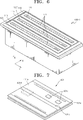
Wie
Die Ladeeinheit
Eine Mehrzahl von Substraten
Die erste Umkehrkammer
Wie
Die Entladeeinheit
Die vorliegende Erfindung ist allerdings nicht auf das vorstehend beschriebene Beispiel beschränkt. Beim Anordnen des Substrats
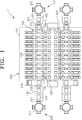
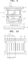
Die Abscheidungseinheit
In diesem Zusammenhang können einige der 11 Baugruppen zur Abscheidung organischer Schichten für die Abscheidung zum Ausbilden einer allgemeinen Schicht genutzt werden und die verbleibenden der 11 Baugruppen zur Abscheidung organischer Schichten können für die Abscheidung zum Auszubilden einer Strukturschicht verwendet werden. Bei dieser Ausführungsform brauchen die Baugruppen zur Abscheidung organischer Schichten, die für die Abscheidung zum Ausbilden einer allgemeinen Schicht genutzt werden, kein Strukturierungsschlitzblatt
Bei der in
Die erste Fördereinheit
Bei der vorliegenden Ausführungsform ist das Gerät zur Abscheidung organischer Schichten
Bei einer Ausführungsform kann die Abscheidungseinheit
Wie
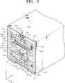
Im Folgenden wird ein Gesamtaufbau der Abscheidungseinheit
Die Kammer
Das obere Gehäuse
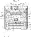
Im Folgenden werden die Komponenten der Baugruppe zur Abscheidung organischer Schichten
Die erste Baugruppe zur Abscheidung organischer Schichten
Um insbesondere ein Abscheidungsmaterial
Das Substrat
Gemäß einer Ausführungsform kann der Abscheidevorgang ausgeführt werden, indem das Substrat
Bei einem herkömmlichen Abscheidungsverfahren unter Verwendung einer FMM muss die Größe der FMM mit der eines Substrates übereinstimmen. Je größer das Substrat ist, umso größer muss daher die FMM sein. Aufgrund dieser Probleme ist es schwierig, die FMM herzustellen und die FMM durch Dehnung der FMM zu einer genauen Strukturierung auszurichten.In a conventional deposition method using an FMM, the size of the FMM must match that of a substrate. The larger the substrate, the larger the FMM must be. Because of these problems, it is difficult to manufacture the FMM and to align the FMM by stretching the FMM to a precise patterning.
Zur Lösung dieser Probleme kann die Abscheidung bei der Baugruppe zur Abscheidung organischer Schichten
Somit kann bei der Baugruppe zur Abscheidung organischer Schichten
Um eine Abscheidung auszuführen, während die Baugruppe zur Abscheidung organischer Schichten
Die Abscheidungsquelle
Die Abscheidungsquelle
Die Abscheidungsquelle
Wie
Wenngleich in
Wie
Bei einer Ausführungsform kann das Strukturierungsschlitzblatt
Bei einer Ausführungsform können die Abscheidungsquelle
Wie vorstehend beschrieben, wird die Abscheidung ausgeführt, während die Baugruppe zur Abscheidung organischer Schichten
Bei einem herkömmlichen Abscheidungsverfahren unter Verwendung einer FMM wird die Abscheidung ausgeführt, während die FMM in engem Kontakt mit einem Substrat steht, um die Entstehung von Schatten auf dem Substrat zu verhindern. Wenn die FMM in engem Kontakt mit dem Substrat ausgebildet ist, können allerdings aufgrund des Kontakts zwischen dem Substrat und der FMM Schäden auftreten. Da es schwierig ist, die Maske relativ zum Substrat zu bewegen, müssen ferner die Maske und das Substrat in derselben Größe ausgebildet sein. Dementsprechend muss die Maske umso größer sein, je größer eine Anzeigevorrichtung ist. Es ist allerdings schwierig, eine große Maske auszubilden.In a conventional deposition process using an FMM, the deposition is performed while the FMM is in intimate contact with a substrate to prevent the formation of shadows on the substrate. However, if the FMM is formed in close contact with the substrate, damage may occur due to the contact between the substrate and the FMM. Further, since it is difficult to move the mask relative to the substrate, the mask and the substrate must be formed in the same size. Accordingly, the larger a display device, the larger the mask must be. However, it is difficult to form a large mask.
Zur Lösung dieser Probleme ist bei der Baugruppe zur Abscheidung organischer Schichten
Gemäß der vorliegenden Ausführungsform kann die Abscheidung ausgeführt werden, während eine Maske, die kleiner als ein Substrat ausgebildet ist, relativ zum Substrat bewegt wird, und somit ist es einfach, die Maske zu fertigen. Darüber hinaus lassen sich Schäden durch den Kontakt zwischen dem Substrat und der Maske vermeiden. Da das Substrat während eines Abscheidevorgangs nicht in engem Kontakt mit der Maske zu stehen braucht, kann ferner die Fertigungsgeschwindigkeit verbessert werden.According to the present embodiment, the deposition can be carried out while a mask formed smaller than a substrate is moved relative to the substrate, and thus it is easy to manufacture the mask. In addition, damage due to contact between the substrate and the mask can be avoided. Further, since the substrate need not be in close contact with the mask during a deposition process, the production speed can be improved.
Im Folgenden werden besondere Anordnungen der einzelnen Elemente des oberen Gehäuses
Die Abscheidungsquelle
In diesem Zusammenhang ist die erste Stufe
Die zweite Stufe
Das Strukturierungsschlitzblatt
Darüber hinaus können das obere Gehäuse
Das Abschirmelement
Um zu verhindern, dass organisches Material auf dem nichtschichtbildenden Bereich des Substrats
Wenn das Substrat
Wie vorstehend beschrieben, wird der nichtschichtbildende Bereich des Substrats
Im Folgenden wird die Fördereinheit
Die erste Fördereinheit
Die zweite Fördereinheit
Die Transfereinheit
Im Folgenden werden die einzelnen Elemente der Fördereinheit
Zunächst wird der Träger
Wie
Das Hauptbauteil
Die Führungsnuten
Die Magnetschiene
Die CPS-Module
Die elektrostatische Einspannvorrichtung
Im Folgenden werden die erste Fördereinheit
Wie
Die Spule
Die Führungselemente
Insbesondere nehmen die Führungselemente
Die seitlichen Magnetlager
Jedes obere Magnetlager
Jedes Führungselement
Magnetische Kräfte der oberen und seitlichen Magnetlager
Im Folgenden wird der Betrieb der Transfereinheit
Der LMS-Magnet
In diesem Zusammenhang kann die Spule
Da der ATM-Kasten
Im Folgenden werden die zweite Fördereinheit
Wie
Die Spule
Wie die erste Fördereinheit
Die Rollenführungen
Die zweite Fördereinheit
Die Baugruppe zur Abscheidung organischer Schichten
Die Kamera
Da das Substrat
Dies bedeutet, dass der Sensor
Da ein Abstand zwischen dem Substrat
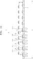
Im Folgenden wird ein Aufbau einer organischen Schicht, die unter Verwendung des vorstehend beschriebenen Geräts zur Abscheidung organischer Schichten
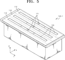
Bei dieser Ausführungsform ist ein Einfallswinkel eines Abscheidungsmaterials, das entlang einer Mittellinie C eines Abscheidungsraums S abgegeben werden soll, im Wesentlichen rechtwinklig zum Substrat
Ein kritischer Einfallswinkel θ des Abscheidungsmaterials, das die Strukturierungsschlitze passiert, die von der Mittellinie C des Abscheidungsraums S weiter entfernt angeordnet sind, wird stufenweise größer, und somit beträgt der kritische Einfallswinkel θ des Abscheidungsmaterials, das den äußersten Strukturierungsschlitz
Dies bedeutet, dass mit zunehmendem kritischem Einfallswinkel θ des Abscheidungsmaterials auch die Größe des Schattens zunimmt. Insbesondere nimmt die Größe des Schattens an einer Position, die weiter von der Mittellinie C des Abscheidungsraums S entfernt ist, zu. Darüber hinaus nimmt mit zunehmendem Abstand zwischen der Mittellinie C des Abscheidungsraum S und den jeweiligen Strukturierungsschlitzen der kritische Einfallswinkel θ des Abscheidungsmaterials zu. Somit weisen organische Schichten, die unter Verwendung des Abscheidungsmaterials ausgebildet wurden, das die weiter von der Mittellinie C des Abscheidungsraums S angeordneten Strukturierungsschlitze passiert, einen größeren Schatten auf. Insbesondere ist von den Schatten auf beiden Seiten der jeweiligen organischen Schichten derjenige Schatten, der sich an einer Position befindet, die weiter von der Mittellinie C des Abscheidungsraums S entfernt ist, größer als der andere.This means that as the critical angle of incidence θ of the deposition material increases, so does the size of the shadow. Specifically, the size of the shadow increases at a position farther from the center line C of the deposition space S. Moreover, as the distance between the center line C of the deposition space S and the respective patterning slots increases, the critical angle of incidence θ of the deposition material increases. Thus, organic layers formed using the deposition material that passes through the patterning slots located farther from the centerline C of the deposition space S have a larger shadow. In particular, of the shadows on both sides of the respective organic layers, that shadow which is located at a position farther from the center line C of the deposition space S is larger than the other.
Dies bedeutet, wie
Außerdem nimmt bei den organischen Schichten, die linksseitig der Mittellinie C des Abscheidungsraums S ausgebildet sind, die Länge der linken Hypotenuse nach links zu. Bei den organischen Schichten, die rechtsseitig der Mittellinie C des Abscheidungsraums S ausgebildet sind, nimmt die Länge der rechten Hypotenuse nach rechts zu. Folglich können die organischen Schichten, die im Abscheidungsraum S ausgebildet sind, bezüglich der Mittellinie C des Abscheidungsraums S symmetrisch zueinander ausgebildet sein.In addition, in the organic layers formed on the left side of the center line C of the deposition space S, the length of the left hypotenuse increases to the left. In the organic layers formed on the right side of the center line C of the deposition space S, the length of the right hypotenuse increases to the right. Thus, the organic layers formed in the deposition space S may be formed symmetrically with respect to the center line C of the deposition space S.
Dieser Aufbau wird im Folgenden genauer beschrieben.This structure will be described in more detail below.
Das Abscheidungsmaterial, das einen Strukturierungsschlitz
In diesem Zusammenhang erfüllen die kritischen Einfallswinkel folgende Bedingung: θb < θc < θd < θe, und somit erfüllen die Größen der Schatten der organischen Schichten ferner folgende Bedingung: SL1 < SL2 < SL3 < SL4 < SL5.In this connection, the critical incident angles satisfy the following condition: θ b <θ c <θ d <θ e , and thus the sizes of the shadows of the organic layers further satisfy the following condition: SL 1 <SL 2 <SL 3 <SL 4 <SL 5 ,
Wie
Auf der Isolierschicht
An einer oberen Fläche der Isolierschicht
In einem der aktiven Halbleiterschicht
Auf der Zwischenschicht-Isolierschicht
Darüber hinaus zeigt die OLED eingestellte oder vorgegebene Bildinformationen an, indem sie gemäß dem Strom rotes, grünes oder blaues Licht emittiert. Die OLED umfasst eine auf der Passivierungsschicht
Eine Pixeldefinitionsschicht
Die Pixeldefinitionsschicht
Die erste Elektrode
Die organische Schicht
Die organische Schicht
Nachdem die organische Schicht
Die erste Elektrode
Die erste Elektrode
Die zweite Elektrode
Das Gerät zur Abscheidung organischer Schichten gemäß den vorstehend beschriebenen Ausführungsformen der vorliegenden Erfindung kann angewandt werden, um eine organische Schicht oder eine anorganische Schicht eines organischen TFT auszubilden und um Schichten aus verschiedenen Materialien auszubilden.The organic film deposition apparatus according to the above-described embodiments of the present invention may be applied to form an organic layer or an inorganic layer of an organic TFT and to form layers of various materials.
Wie vorstehend beschrieben, stellen die eine oder mehreren Ausführungsformen der vorliegenden Erfindung Geräte zur Abscheidung organischer Schichten, die zur Verwendung in der Massenfertigung eines großen Substrats geeignet sind und eine hochauflösende Strukturierung ermöglichen, Verfahren zur Fertigung von Vorrichtung mit organischer lichtemittierender Anzeige unter Verwendung derselben und unter Verwendung des Verfahrens gefertigte Vorrichtungen mit organischer lichtemittierender Anzeige bereit. Wenngleich nur einige Ausführungsformen der vorliegenden Erfindung gezeigt und beschrieben wurden, wird der Fachmann erkennen, dass an dieser Ausführungsform Änderungen vorgenommen werden können, ohne von den Grundsätzen der Erfindung, deren Umfang in den Ansprüchen und deren Entsprechungen definiert ist, abzuweichen.As described above, the one or more embodiments of the present invention provide organic layer deposition apparatuses suitable for use in mass production of a large substrate and enabling high resolution patterning, methods of fabricating an organic light emitting display device using the same and others Use of the method prepared devices with organic light emitting display ready. Although only a few embodiments of the present invention have been shown and described, it will be appreciated by those skilled in the art that changes may be made to this embodiment without departing from the principles of the invention, the scope of which is defined in the claims and their equivalents.
Claims (40)
Applications Claiming Priority (2)
| Application Number | Priority Date | Filing Date | Title |
|---|---|---|---|
| KR10-2012-0067303 | 2012-06-22 | ||
| KR1020120067303A KR102015872B1 (en) | 2012-06-22 | 2012-06-22 | Apparatus for organic layer deposition, method for manufacturing of organic light emitting display apparatus using the same, and organic light emitting display apparatus manufactured by the method |
Publications (1)
| Publication Number | Publication Date |
|---|---|
| DE102012222927A1 true DE102012222927A1 (en) | 2013-12-24 |
Family
ID=49713801
Family Applications (1)
| Application Number | Title | Priority Date | Filing Date |
|---|---|---|---|
| DE102012222927A Pending DE102012222927A1 (en) | 2012-06-22 | 2012-12-12 | Organic layer deposition apparatus, method of manufacturing organic light emitting display devices using the same and organic light emitting display devices manufactured using the method |
Country Status (6)
| Country | Link |
|---|---|
| US (1) | US9260778B2 (en) |
| JP (1) | JP6272662B2 (en) |
| KR (1) | KR102015872B1 (en) |
| CN (2) | CN103515543B (en) |
| DE (1) | DE102012222927A1 (en) |
| TW (1) | TWI594477B (en) |
Families Citing this family (42)
| Publication number | Priority date | Publication date | Assignee | Title |
|---|---|---|---|---|
| JP5328726B2 (en) | 2009-08-25 | 2013-10-30 | 三星ディスプレイ株式會社 | Thin film deposition apparatus and organic light emitting display device manufacturing method using the same |
| JP5677785B2 (en) | 2009-08-27 | 2015-02-25 | 三星ディスプレイ株式會社Samsung Display Co.,Ltd. | Thin film deposition apparatus and organic light emitting display device manufacturing method using the same |
| US8876975B2 (en) | 2009-10-19 | 2014-11-04 | Samsung Display Co., Ltd. | Thin film deposition apparatus |
| KR101084184B1 (en) | 2010-01-11 | 2011-11-17 | 삼성모바일디스플레이주식회사 | Apparatus for thin layer deposition |
| KR101193186B1 (en) | 2010-02-01 | 2012-10-19 | 삼성디스플레이 주식회사 | Apparatus for thin layer deposition, method for manufacturing of organic light emitting display apparatus using the same, and organic light emitting display apparatus manufactured by the method |
| KR101156441B1 (en) | 2010-03-11 | 2012-06-18 | 삼성모바일디스플레이주식회사 | Apparatus for thin layer deposition |
| US8894458B2 (en) | 2010-04-28 | 2014-11-25 | Samsung Display Co., Ltd. | Thin film deposition apparatus, method of manufacturing organic light-emitting display device by using the apparatus, and organic light-emitting display device manufactured by using the method |
| KR101223723B1 (en) | 2010-07-07 | 2013-01-18 | 삼성디스플레이 주식회사 | Apparatus for thin layer deposition, method for manufacturing of organic light emitting display apparatus using the same, and organic light emitting display apparatus manufactured by the method |
| KR101723506B1 (en) | 2010-10-22 | 2017-04-19 | 삼성디스플레이 주식회사 | Apparatus for organic layer deposition and method for manufacturing of organic light emitting display apparatus using the same |
| KR101738531B1 (en) | 2010-10-22 | 2017-05-23 | 삼성디스플레이 주식회사 | Method for manufacturing of organic light emitting display apparatus, and organic light emitting display apparatus manufactured by the method |
| KR20120045865A (en) | 2010-11-01 | 2012-05-09 | 삼성모바일디스플레이주식회사 | Apparatus for organic layer deposition |
| KR20120065789A (en) | 2010-12-13 | 2012-06-21 | 삼성모바일디스플레이주식회사 | Apparatus for organic layer deposition |
| KR101760897B1 (en) | 2011-01-12 | 2017-07-25 | 삼성디스플레이 주식회사 | Deposition source and apparatus for organic layer deposition having the same |
| KR101840654B1 (en) | 2011-05-25 | 2018-03-22 | 삼성디스플레이 주식회사 | Apparatus for organic layer deposition and method for manufacturing of organic light emitting display apparatus using the same |
| KR101852517B1 (en) | 2011-05-25 | 2018-04-27 | 삼성디스플레이 주식회사 | Apparatus for organic layer deposition and method for manufacturing of organic light emitting display apparatus using the same |
| KR101857249B1 (en) | 2011-05-27 | 2018-05-14 | 삼성디스플레이 주식회사 | Patterning slit sheet assembly, apparatus for organic layer deposition, method for manufacturing organic light emitting display apparatus and organic light emitting display apparatus |
| KR101826068B1 (en) | 2011-07-04 | 2018-02-07 | 삼성디스플레이 주식회사 | Apparatus for thin layer deposition |
| KR20130004830A (en) | 2011-07-04 | 2013-01-14 | 삼성디스플레이 주식회사 | Apparatus for thin layer deposition and method for manufacturing of organic light emitting display apparatus using the same |
| KR101461037B1 (en) * | 2012-02-29 | 2014-11-13 | 엘지디스플레이 주식회사 | Apparatus and method of fabricating organic electroluminescence device |
| KR102015872B1 (en) * | 2012-06-22 | 2019-10-22 | 삼성디스플레이 주식회사 | Apparatus for organic layer deposition, method for manufacturing of organic light emitting display apparatus using the same, and organic light emitting display apparatus manufactured by the method |
| KR101959974B1 (en) * | 2012-07-10 | 2019-07-16 | 삼성디스플레이 주식회사 | Apparatus for organic layer deposition, method for manufacturing of organic light emitting display apparatus using the same, and organic light emitting display apparatus manufactured by the method |
| CN103545460B (en) * | 2012-07-10 | 2017-04-12 | 三星显示有限公司 | Organic light-emitting display device, organic light-emitting display apparatus, and method of manufacturing organic light-emitting display apparatus |
| KR101994838B1 (en) * | 2012-09-24 | 2019-10-01 | 삼성디스플레이 주식회사 | Apparatus for organic layer deposition, method for manufacturing of organic light emitting display apparatus using the same, and organic light emitting display apparatus manufactured by the method |
| KR102084696B1 (en) * | 2013-01-23 | 2020-03-05 | 삼성디스플레이 주식회사 | Thin layer deposition apparatus for display device, mask unit for depositing thin layer in display device, display device and method of manufacturing the same |
| KR102081284B1 (en) * | 2013-04-18 | 2020-02-26 | 삼성디스플레이 주식회사 | Deposition apparatus, method for manufacturing organic light emitting display apparatus using the same, and organic light emitting display apparatus manufactured by the same |
| KR102098741B1 (en) * | 2013-05-27 | 2020-04-09 | 삼성디스플레이 주식회사 | Substrate transfer unit for deposition, apparatus for organic layer deposition comprising the same, and method for manufacturing of organic light emitting display apparatus using the same |
| KR102096887B1 (en) * | 2013-05-30 | 2020-04-06 | 삼성디스플레이 주식회사 | Organic light emitting display device and method manufacturing the same |
| KR102086550B1 (en) * | 2013-05-31 | 2020-03-10 | 삼성디스플레이 주식회사 | Deposition apparatus, method for manufacturing organic light emitting display apparatus using the same, and organic light emitting display apparatus manufactured by the same |
| KR102162797B1 (en) * | 2013-12-23 | 2020-10-08 | 삼성디스플레이 주식회사 | Method for manufacturing of organic light emitting display apparatus |
| KR102211969B1 (en) * | 2014-01-03 | 2021-02-05 | 삼성디스플레이 주식회사 | Depostion device |
| KR102391346B1 (en) * | 2015-08-04 | 2022-04-28 | 삼성디스플레이 주식회사 | Organic light display apparatus, apparatus for organic layer deposition, and method for manufacturing of organic light emitting display apparatus using the same |
| KR102109375B1 (en) * | 2015-10-02 | 2020-05-12 | 주식회사 원익아이피에스 | Device for aligning substrate |
| KR102432348B1 (en) * | 2015-12-04 | 2022-08-16 | 삼성디스플레이 주식회사 | Apparatus for organic layer deposition, and method for manufacturing of organic light emitting display apparatus using the same |
| KR102519797B1 (en) * | 2016-04-12 | 2023-04-10 | 삼성디스플레이 주식회사 | Deposition apparatus and deposition |
| KR102610026B1 (en) * | 2016-06-30 | 2023-12-06 | 삼성디스플레이 주식회사 | Organic light-emitting display apparatus and method for manufacturing the same |
| WO2018110953A1 (en) * | 2016-12-12 | 2018-06-21 | Applied Materials, Inc. | Substrate processing apparatus and method using the same |
| WO2019081043A1 (en) * | 2017-10-27 | 2019-05-02 | Applied Materials, Inc. | Carrier for contactless transportation in a deposition system, apparatus for contactless transportation of a carrier, and method for contactless transportation of a carrier in a deposition system |
| CN108893709B (en) * | 2018-02-11 | 2021-04-06 | 清华大学 | Mask-substrate spacing control system for direct-write vacuum evaporation system |
| JP7249142B2 (en) * | 2018-12-14 | 2023-03-30 | キヤノントッキ株式会社 | Transport carriers, vapor deposition equipment, and electronic device manufacturing equipment |
| JP7316782B2 (en) * | 2018-12-14 | 2023-07-28 | キヤノントッキ株式会社 | Vapor deposition apparatus, electronic device manufacturing apparatus, and vapor deposition method |
| US11856833B2 (en) | 2020-01-22 | 2023-12-26 | Applied Materials, Inc. | In-line monitoring of OLED layer thickness and dopant concentration |
| KR20220129598A (en) * | 2020-01-22 | 2022-09-23 | 어플라이드 머티어리얼스, 인코포레이티드 | In-line monitoring of OLED layer thickness and dopant concentration |
Family Cites Families (146)
| Publication number | Priority date | Publication date | Assignee | Title |
|---|---|---|---|---|
| JPS6053745B2 (en) | 1981-07-31 | 1985-11-27 | アルバツク成膜株式会社 | Method for forming heterogeneous optical thin films by binary deposition |
| JPH02247372A (en) | 1989-03-17 | 1990-10-03 | Mitsubishi Electric Corp | Thin film formation |
| JP3125279B2 (en) | 1991-02-25 | 2001-01-15 | 東海カーボン株式会社 | Graphite crucible for vacuum evaporation |
| JP3395801B2 (en) | 1994-04-28 | 2003-04-14 | 株式会社ニコン | Catadioptric projection optical system, scanning projection exposure apparatus, and scanning projection exposure method |
| JPH0851137A (en) * | 1994-08-08 | 1996-02-20 | Shinko Electric Co Ltd | Transferring device for semiconductor manufacturing apparatus |
| JPH0995776A (en) | 1995-09-29 | 1997-04-08 | Sony Corp | Vacuum deposition device |
| JPH1050478A (en) | 1996-04-19 | 1998-02-20 | Toray Ind Inc | Organic field emission element and manufacture thereof |
| US6274198B1 (en) | 1997-02-24 | 2001-08-14 | Agere Systems Optoelectronics Guardian Corp. | Shadow mask deposition |
| KR100257219B1 (en) | 1997-10-23 | 2000-05-15 | 박용관 | Method and device for making a safety operation of a polyethylene gas pipe valve arrangement |
| JP2000068054A (en) | 1998-08-26 | 2000-03-03 | Hokuriku Electric Ind Co Ltd | Manufacture of el element |
| KR20000019254A (en) | 1998-09-08 | 2000-04-06 | 석창길 | Device for improving thin film thickness uniformity of cvd |
| US6384529B2 (en) | 1998-11-18 | 2002-05-07 | Eastman Kodak Company | Full color active matrix organic electroluminescent display panel having an integrated shadow mask |
| CA2374448A1 (en) | 1999-01-26 | 2000-08-03 | Dbs Beschichtung Und Systeme-Technik Gmbh | Method for coating the inside of pipes and coating system |
| JP2001052862A (en) | 1999-08-04 | 2001-02-23 | Hokuriku Electric Ind Co Ltd | Manufacture of organic el element and device therefor |
| JP4187367B2 (en) | 1999-09-28 | 2008-11-26 | 三洋電機株式会社 | ORGANIC LIGHT EMITTING ELEMENT, ITS MANUFACTURING DEVICE, AND ITS MANUFACTURING METHOD |
| TW474114B (en) | 1999-09-29 | 2002-01-21 | Junji Kido | Organic electroluminescent device, organic electroluminescent device assembly and method of controlling the emission spectrum in the device |
| AU3331700A (en) | 1999-10-29 | 2001-05-08 | E. One Co., Ltd. | Scent diffusion apparatus and method thereof |
| KR100302159B1 (en) | 1999-10-29 | 2001-09-22 | 최중호 | Scent diffusion apparatus and method therefor |
| TW490714B (en) | 1999-12-27 | 2002-06-11 | Semiconductor Energy Lab | Film formation apparatus and method for forming a film |
| KR100653515B1 (en) | 1999-12-30 | 2006-12-04 | 주식회사 팬택앤큐리텔 | Mobile station for mobile communication system |
| JP3754859B2 (en) | 2000-02-16 | 2006-03-15 | キヤノン株式会社 | Manufacturing method of image display device |
| JP4053209B2 (en) | 2000-05-01 | 2008-02-27 | 三星エスディアイ株式会社 | Manufacturing method of organic EL display |
| EP1167566B1 (en) | 2000-06-22 | 2011-01-26 | Panasonic Electric Works Co., Ltd. | Apparatus for and method of vacuum vapor deposition |
| KR20020000201A (en) | 2000-06-23 | 2002-01-05 | 최승락 | Method cleaning Liquid Chrystal Display using Laser and Vapor Phase |
| JP2002175878A (en) | 2000-09-28 | 2002-06-21 | Sanyo Electric Co Ltd | Forming method of layer, and manufacturing method of color luminous device |
| KR100726132B1 (en) | 2000-10-31 | 2007-06-12 | 엘지.필립스 엘시디 주식회사 | A method for fabricating array substrate for liquid crystal display device and the same |
| US7078070B2 (en) | 2000-11-07 | 2006-07-18 | Helix Technology Inc. | Method for fabricating an organic light emitting diode |
| US6468496B2 (en) | 2000-12-21 | 2002-10-22 | Arco Chemical Technology, L.P. | Process for producing hydrogen peroxide |
| KR100625403B1 (en) | 2000-12-22 | 2006-09-18 | 주식회사 하이닉스반도체 | Virtual Channel SDRAM |
| KR100698033B1 (en) | 2000-12-29 | 2007-03-23 | 엘지.필립스 엘시디 주식회사 | Organic Electroluminescence Device and Fabrication Method for the same |
| KR100405080B1 (en) | 2001-05-11 | 2003-11-10 | 엘지.필립스 엘시디 주식회사 | A method of crystallizing Si |
| KR100463212B1 (en) | 2001-05-19 | 2004-12-23 | 주식회사 아이엠티 | Apparatus for dry surface-cleaning of materials |
| JP4704605B2 (en) | 2001-05-23 | 2011-06-15 | 淳二 城戸 | Continuous vapor deposition apparatus, vapor deposition apparatus and vapor deposition method |
| JP2003077662A (en) | 2001-06-22 | 2003-03-14 | Junji Kido | Method and device for manufacturing organic electroluminescent element |
| JP2003003250A (en) | 2001-06-22 | 2003-01-08 | Alps Electric Co Ltd | Vacuum deposition polymerization system and method for depositing organic film using the system |
| JP3705237B2 (en) | 2001-09-05 | 2005-10-12 | ソニー株式会社 | Display device manufacturing system and method using organic electroluminescent element |
| TW591202B (en) | 2001-10-26 | 2004-06-11 | Hermosa Thin Film Co Ltd | Dynamic film thickness control device/method and ITS coating method |
| US20030101937A1 (en) | 2001-11-28 | 2003-06-05 | Eastman Kodak Company | Thermal physical vapor deposition source for making an organic light-emitting device |
| JP3481232B2 (en) * | 2002-03-05 | 2003-12-22 | 三洋電機株式会社 | Manufacturing method of organic electroluminescence panel |
| US20030168013A1 (en) | 2002-03-08 | 2003-09-11 | Eastman Kodak Company | Elongated thermal physical vapor deposition source with plural apertures for making an organic light-emitting device |
| JP2003297562A (en) | 2002-03-29 | 2003-10-17 | Sanyo Electric Co Ltd | Vapor deposition method |
| US6749906B2 (en) | 2002-04-25 | 2004-06-15 | Eastman Kodak Company | Thermal physical vapor deposition apparatus with detachable vapor source(s) and method |
| ES2677348T3 (en) | 2002-05-03 | 2018-08-01 | The Government Of The United States Of America, As Represented By The Secretary, Department Of Health And Human Services | A recombinant chimeric dengue virus rDEN3 / 4delta 30 (ME), rDEN2 / 4delta30 (ME) or rDEN1 / 4delta30 (ME) that contains a deletion of 30 nucleotides (delta30) in a section of the 3 'non-translated region of the genome of type 4 dengue, wherein said 30 nucleotide deletion corresponds to the stem-loop structure of TL2 |
| US20030232563A1 (en) | 2002-05-09 | 2003-12-18 | Isao Kamiyama | Method and apparatus for manufacturing organic electroluminescence device, and system and method for manufacturing display unit using organic electroluminescence devices |
| JP4292777B2 (en) | 2002-06-17 | 2009-07-08 | ソニー株式会社 | Thin film forming equipment |
| KR100908232B1 (en) | 2002-06-03 | 2009-07-20 | 삼성모바일디스플레이주식회사 | Mask frame assembly for thin film deposition of organic electroluminescent device |
| JP4440563B2 (en) | 2002-06-03 | 2010-03-24 | 三星モバイルディスプレイ株式會社 | Mask frame assembly for thin film deposition of organic electroluminescent devices |
| US20030221620A1 (en) * | 2002-06-03 | 2003-12-04 | Semiconductor Energy Laboratory Co., Ltd. | Vapor deposition device |
| JP2004043898A (en) | 2002-07-12 | 2004-02-12 | Canon Electronics Inc | Vapor deposition mask, and organic electroluminescence display device |
| KR100397196B1 (en) | 2002-08-27 | 2003-09-13 | 에이엔 에스 주식회사 | Organic material point source feeding unit in organic semiconductor device and method thereof |
| JP2004103269A (en) | 2002-09-05 | 2004-04-02 | Sanyo Electric Co Ltd | Manufacture method for organic electroluminescence display device |
| TWI252706B (en) | 2002-09-05 | 2006-04-01 | Sanyo Electric Co | Manufacturing method of organic electroluminescent display device |
| JP2004103341A (en) | 2002-09-09 | 2004-04-02 | Matsushita Electric Ind Co Ltd | Manufacturing method of organic electroluminescent element |
| US6911671B2 (en) | 2002-09-23 | 2005-06-28 | Eastman Kodak Company | Device for depositing patterned layers in OLED displays |
| US20040086639A1 (en) | 2002-09-24 | 2004-05-06 | Grantham Daniel Harrison | Patterned thin-film deposition using collimating heated mask asembly |
| JP4139186B2 (en) | 2002-10-21 | 2008-08-27 | 東北パイオニア株式会社 | Vacuum deposition equipment |
| JP2004143521A (en) | 2002-10-24 | 2004-05-20 | Sony Corp | Thin-film deposition device |
| JP2004183044A (en) | 2002-12-03 | 2004-07-02 | Seiko Epson Corp | Mask vapor deposition method and apparatus, mask and mask manufacturing method, display panel manufacturing apparatus, display panel and electronic equipment |
| JP2004199919A (en) | 2002-12-17 | 2004-07-15 | Tohoku Pioneer Corp | Method for manufacturing organic el display panel |
| JP2004207142A (en) | 2002-12-26 | 2004-07-22 | Seiko Epson Corp | Manufacturing method for organic electroluminescent device, organic electroluminescent device, and electronic equipment |
| KR100646160B1 (en) | 2002-12-31 | 2006-11-14 | 엘지.필립스 엘시디 주식회사 | A mask for sequential lateral solidification and a silicon crystallizing method using the same |
| US20040144321A1 (en) | 2003-01-28 | 2004-07-29 | Eastman Kodak Company | Method of designing a thermal physical vapor deposition system |
| JP3966292B2 (en) | 2003-03-27 | 2007-08-29 | セイコーエプソン株式会社 | Pattern forming method and pattern forming apparatus, device manufacturing method, conductive film wiring, electro-optical device, and electronic apparatus |
| JP2007500794A (en) | 2003-05-16 | 2007-01-18 | エスブイティー アソーシエイツ インコーポレイテッド | Thin film evaporation evaporator |
| JP2004349101A (en) | 2003-05-22 | 2004-12-09 | Seiko Epson Corp | Film forming method, film forming device, manufacturing method of organic electroluminescent device, and organic electroluminescent device |
| US6837939B1 (en) | 2003-07-22 | 2005-01-04 | Eastman Kodak Company | Thermal physical vapor deposition source using pellets of organic material for making OLED displays |
| JP2005044592A (en) | 2003-07-28 | 2005-02-17 | Toyota Industries Corp | Depositing mask, film formation method using it, and film formation device using it |
| KR100889764B1 (en) | 2003-10-04 | 2009-03-20 | 삼성모바일디스플레이주식회사 | Mask frame assembly for depositing thin layer of organic electro luminescence device and deposition method using the same |
| KR100520159B1 (en) | 2003-11-12 | 2005-10-10 | 삼성전자주식회사 | Apparatus and method for interference cancellation of ofdm system using multiple antenna |
| JP4475967B2 (en) | 2004-01-29 | 2010-06-09 | 三菱重工業株式会社 | Vacuum evaporation machine |
| JP4441282B2 (en) | 2004-02-02 | 2010-03-31 | 富士フイルム株式会社 | Vapor deposition mask and organic EL display device manufacturing method |
| US20050166844A1 (en) | 2004-02-03 | 2005-08-04 | Nicholas Gralenski | High reflectivity atmospheric pressure furnace for preventing contamination of a work piece |
| JP2005235568A (en) | 2004-02-19 | 2005-09-02 | Seiko Epson Corp | Deposition device and manufacturing device of organic el device |
| JP2005293968A (en) | 2004-03-31 | 2005-10-20 | Sanyo Electric Co Ltd | Manufacturing method of organic electroluminescent element |
| JP2005296737A (en) | 2004-04-07 | 2005-10-27 | Mikuni Corp | Beat plate |
| US20050244580A1 (en) | 2004-04-30 | 2005-11-03 | Eastman Kodak Company | Deposition apparatus for temperature sensitive materials |
| JP4455937B2 (en) | 2004-06-01 | 2010-04-21 | 東北パイオニア株式会社 | Deposition source, vacuum film formation apparatus, organic EL panel manufacturing method |
| KR20060008602A (en) | 2004-07-21 | 2006-01-27 | 엘지전자 주식회사 | Method for depositing organic electroluminescent layer |
| US7273663B2 (en) | 2004-08-20 | 2007-09-25 | Eastman Kodak Company | White OLED having multiple white electroluminescence units |
| KR100579406B1 (en) | 2004-08-25 | 2006-05-12 | 삼성에스디아이 주식회사 | Vertical Moving Type Apparatus for Depositing Organic Material |
| KR101070539B1 (en) | 2004-09-08 | 2011-10-05 | 도레이 카부시키가이샤 | Deposition mask and manufacturing method of organic electroluminescent device using the same |
| EP1802177A4 (en) | 2004-09-08 | 2010-04-14 | Toray Industries | Organic electroluminescent device and manufacturing method thereof |
| JP2006147488A (en) * | 2004-11-24 | 2006-06-08 | Canon Inc | Manufacturing apparatus for organic el element |
| KR20060060994A (en) | 2004-12-01 | 2006-06-07 | 삼성에스디아이 주식회사 | Deposition source and deposition apparatus therewith |
| KR100700641B1 (en) | 2004-12-03 | 2007-03-27 | 삼성에스디아이 주식회사 | Laser irradiation device, patterning method and fabrication method of organic electroluminescence display device using the same |
| KR20060073367A (en) | 2004-12-24 | 2006-06-28 | 엘지전자 주식회사 | Apparatus for organic matter treatment of cleaning room |
| JP4384109B2 (en) | 2005-01-05 | 2009-12-16 | 三星モバイルディスプレイ株式會社 | Drive shaft of vapor deposition source for vapor deposition system and vapor deposition system having the same |
| KR100645719B1 (en) | 2005-01-05 | 2006-11-14 | 삼성에스디아이 주식회사 | Effusion cell for depositing material and deposition apparatus having it |
| KR100600357B1 (en) | 2005-01-05 | 2006-07-18 | 삼성에스디아이 주식회사 | Apparatus for sealing the driving shaft for the effusion cell in the deposition system and deposition system having it |
| KR100796148B1 (en) | 2005-01-05 | 2008-01-21 | 삼성에스디아이 주식회사 | Vertical movement type effusion cell for depositing material and deposition system having it |
| KR20060083510A (en) | 2005-01-17 | 2006-07-21 | 삼성전자주식회사 | Photomask apparatus removing defective byproducts of a photomask |
| KR100666574B1 (en) | 2005-01-31 | 2007-01-09 | 삼성에스디아이 주식회사 | Vapor deposition source |
| JP4440837B2 (en) | 2005-01-31 | 2010-03-24 | 三星モバイルディスプレイ株式會社 | Evaporation source and vapor deposition apparatus employing the same |
| KR100719314B1 (en) | 2005-03-31 | 2007-05-17 | 세메스 주식회사 | Apparatus for transferring substrate and apparatus for depositing organic film on substrate |
| US7918940B2 (en) | 2005-02-07 | 2011-04-05 | Semes Co., Ltd. | Apparatus for processing substrate |
| KR100687007B1 (en) | 2005-03-22 | 2007-02-26 | 세메스 주식회사 | Apparatus for depositing organic film used in manufacturing organicelectro luminescence device |
| JP2006275433A (en) | 2005-03-29 | 2006-10-12 | National Institute Of Advanced Industrial & Technology | Absorption type small cooling and refrigerating device |
| KR100637714B1 (en) | 2005-03-31 | 2006-10-25 | 세메스 주식회사 | Apparatus for treating substrate |
| KR100773249B1 (en) | 2005-04-18 | 2007-11-05 | 엘지전자 주식회사 | Mask used for forming an electroluminescent layer |
| EP1717339A2 (en) * | 2005-04-20 | 2006-11-02 | Applied Films GmbH & Co. KG | Continuous coating apparatus |
| KR100700493B1 (en) | 2005-05-24 | 2007-03-28 | 삼성에스디아이 주식회사 | Catalytic Enhanced Chemical Vapor Deposition Apparatus having Effective filament of Arrangement Structure |
| KR100797787B1 (en) | 2005-06-03 | 2008-01-24 | 주식회사 아이엠티 | Dry cleaning system using a laser |
| US7432201B2 (en) * | 2005-07-19 | 2008-10-07 | Applied Materials, Inc. | Hybrid PVD-CVD system |
| US20070017445A1 (en) * | 2005-07-19 | 2007-01-25 | Takako Takehara | Hybrid PVD-CVD system |
| JP4655812B2 (en) | 2005-08-08 | 2011-03-23 | カシオ計算機株式会社 | Musical sound generator and program |
| KR100711885B1 (en) | 2005-08-31 | 2007-04-25 | 삼성에스디아이 주식회사 | Source for organic layer and the method for controlling heating source thereof |
| KR20070035796A (en) | 2005-09-28 | 2007-04-02 | 엘지전자 주식회사 | Apparatus for fabricating organic electro luminescence display device |
| KR100697663B1 (en) | 2005-10-27 | 2007-03-20 | 세메스 주식회사 | Apparatus for deposition organic compounds |
| JP4767000B2 (en) | 2005-11-28 | 2011-09-07 | 日立造船株式会社 | Vacuum deposition equipment |
| KR100696547B1 (en) | 2005-12-09 | 2007-03-19 | 삼성에스디아이 주식회사 | Method for depositing film |
| JP5064810B2 (en) | 2006-01-27 | 2012-10-31 | キヤノン株式会社 | Vapor deposition apparatus and vapor deposition method |
| KR20070080635A (en) | 2006-02-08 | 2007-08-13 | 주식회사 아바코 | Organic boat |
| WO2007099929A1 (en) * | 2006-02-28 | 2007-09-07 | Ulvac, Inc. | Organic thin film depositing method and organic thin film depositing apparatus |
| JP2007270188A (en) * | 2006-03-30 | 2007-10-18 | Hoya Corp | Film forming equipment |
| KR20070105595A (en) | 2006-04-27 | 2007-10-31 | 두산메카텍 주식회사 | Evaporation apparatus |
| KR100770653B1 (en) | 2006-05-25 | 2007-10-29 | 에이엔 에스 주식회사 | Depositing apparatus forming thin film |
| KR101248004B1 (en) | 2006-06-29 | 2013-03-27 | 엘지디스플레이 주식회사 | A deposit system for OLED and method of fabricating of OLED using the same |
| KR100800125B1 (en) | 2006-06-30 | 2008-01-31 | 세메스 주식회사 | Source shutter and substrate control method of Organic Light-Emitting DeviceOLED evaporation apparatus |
| KR100980729B1 (en) | 2006-07-03 | 2010-09-07 | 주식회사 야스 | Multiple nozzle evaporator for vacuum thermal evaporation |
| KR100723627B1 (en) | 2006-08-01 | 2007-06-04 | 세메스 주식회사 | Evaporator for organic thin film vapor deposition |
| KR100815265B1 (en) | 2006-08-28 | 2008-03-19 | 주식회사 대우일렉트로닉스 | Method for manufacturing micro heater and crucible, and vacuum deposition apparatus of organic substances having the micro heater and crucible |
| KR100823508B1 (en) | 2006-10-19 | 2008-04-21 | 삼성에스디아이 주식회사 | Evaporation source and organic matter sputtering apparatus with the same |
| KR100839380B1 (en) | 2006-10-30 | 2008-06-19 | 삼성에스디아이 주식회사 | Vacuum evaporation apparatus for organic light emission display |
| JP4768584B2 (en) | 2006-11-16 | 2011-09-07 | 財団法人山形県産業技術振興機構 | Evaporation source and vacuum deposition apparatus using the same |
| KR20080045886A (en) | 2006-11-21 | 2008-05-26 | 삼성전자주식회사 | Big-size hybrid open mask and manufacturing is packaged and manufacturing method of organic electro-luminescence display the same |
| US20080131587A1 (en) | 2006-11-30 | 2008-06-05 | Boroson Michael L | Depositing organic material onto an oled substrate |
| KR20080060400A (en) | 2006-12-27 | 2008-07-02 | 엘지디스플레이 주식회사 | Method of manufacturing array substrate and method of manufacturing organic light emitting device using the method |
| KR20080061132A (en) | 2006-12-28 | 2008-07-02 | 엘지디스플레이 주식회사 | Apparatus for forming organic layer |
| KR20080062212A (en) | 2006-12-29 | 2008-07-03 | 세메스 주식회사 | Apparatus for depositing organic film on substrate |
| JP5081516B2 (en) | 2007-07-12 | 2012-11-28 | 株式会社ジャパンディスプレイイースト | Vapor deposition method and vapor deposition apparatus |
| JP4974832B2 (en) | 2007-09-10 | 2012-07-11 | 株式会社アルバック | Vapor deposition source, vapor deposition equipment |
| KR20090038733A (en) | 2007-10-16 | 2009-04-21 | 주식회사 실트론 | Heat treatment method for improvement of surface roughness of soi-wafer and apparatus for the same |
| KR20090079765A (en) | 2008-01-17 | 2009-07-22 | 이태환 | A power-driven machinery that is utilized gravity |
| KR100994114B1 (en) | 2008-03-11 | 2010-11-12 | 삼성모바일디스플레이주식회사 | Evaporating method for forming thin film |
| KR100922763B1 (en) | 2008-03-13 | 2009-10-21 | 삼성모바일디스플레이주식회사 | Organic light emitting display apparatus and method of manufacturing thereof |
| US7943202B2 (en) | 2008-05-07 | 2011-05-17 | Qualcomm Mems Technologies, Inc. | Apparatus and methods for providing a static interferometric display device |
| KR20100002381A (en) | 2008-06-30 | 2010-01-07 | (주)드림젯코리아 | The flat-board printer |
| JP5277015B2 (en) * | 2009-02-13 | 2013-08-28 | 株式会社日立ハイテクノロジーズ | Organic EL device manufacturing apparatus, film forming apparatus, and shadow mask exchange apparatus |
| KR101097311B1 (en) * | 2009-06-24 | 2011-12-21 | 삼성모바일디스플레이주식회사 | Organic light emitting display apparatus and apparatus for thin layer deposition for manufacturing the same |
| JP5677785B2 (en) * | 2009-08-27 | 2015-02-25 | 三星ディスプレイ株式會社Samsung Display Co.,Ltd. | Thin film deposition apparatus and organic light emitting display device manufacturing method using the same |
| KR101174877B1 (en) * | 2009-08-27 | 2012-08-17 | 삼성디스플레이 주식회사 | Apparatus for thin layer deposition and method for manufacturing of organic light emitting display apparatus using the same |
| KR101193192B1 (en) * | 2009-09-01 | 2012-10-19 | 삼성디스플레이 주식회사 | Apparatus for thin layer deposition |
| KR101084184B1 (en) * | 2010-01-11 | 2011-11-17 | 삼성모바일디스플레이주식회사 | Apparatus for thin layer deposition |
| KR101156441B1 (en) * | 2010-03-11 | 2012-06-18 | 삼성모바일디스플레이주식회사 | Apparatus for thin layer deposition |
| WO2012046672A1 (en) * | 2010-10-04 | 2012-04-12 | 東京エレクトロン株式会社 | Deposition apparatus and deposition material supply method |
| KR102015872B1 (en) * | 2012-06-22 | 2019-10-22 | 삼성디스플레이 주식회사 | Apparatus for organic layer deposition, method for manufacturing of organic light emitting display apparatus using the same, and organic light emitting display apparatus manufactured by the method |
-
2012
- 2012-06-22 KR KR1020120067303A patent/KR102015872B1/en active IP Right Grant
- 2012-10-17 US US13/654,378 patent/US9260778B2/en active Active
- 2012-11-20 TW TW101143351A patent/TWI594477B/en active
- 2012-12-12 DE DE102012222927A patent/DE102012222927A1/en active Pending
-
2013
- 2013-05-13 CN CN201310174098.8A patent/CN103515543B/en active Active
- 2013-05-13 CN CN2013202576435U patent/CN203351668U/en not_active Expired - Lifetime
- 2013-06-21 JP JP2013130320A patent/JP6272662B2/en active Active
Also Published As
| Publication number | Publication date |
|---|---|
| US9260778B2 (en) | 2016-02-16 |
| CN103515543A (en) | 2014-01-15 |
| CN103515543B (en) | 2018-03-27 |
| KR102015872B1 (en) | 2019-10-22 |
| TWI594477B (en) | 2017-08-01 |
| JP6272662B2 (en) | 2018-01-31 |
| CN203351668U (en) | 2013-12-18 |
| KR20140000041A (en) | 2014-01-02 |
| JP2014005536A (en) | 2014-01-16 |
| TW201401609A (en) | 2014-01-01 |
| US20130341598A1 (en) | 2013-12-26 |
Similar Documents
| Publication | Publication Date | Title |
|---|---|---|
| DE102012222927A1 (en) | Organic layer deposition apparatus, method of manufacturing organic light emitting display devices using the same and organic light emitting display devices manufactured using the method | |
| DE102012222673A1 (en) | Organic layer deposition apparatus, method of manufacturing organic light emitting display devices using the same, and organic light emitting display device | |
| DE102012222672A1 (en) | Organic layer deposition apparatus and method for manufacturing organic light devices of the display using the same | |
| US9306191B2 (en) | Organic light-emitting display apparatus and method of manufacturing the same | |
| DE102011017648B4 (en) | A thin film deposition apparatus, a method of manufacturing an organic light emitting display using the thin film deposition apparatus and an organic light emitting display produced by the method | |
| US10431779B2 (en) | Organic layer deposition apparatus, method of manufacturing organic light-emitting display apparatus using the same, and organic light-emitting display apparatus manufactured using the method | |
| DE102011005419A1 (en) | Thin-film deposition apparatus | |
| KR101959975B1 (en) | Apparatus for organic layer deposition, method for manufacturing of organic light emitting display apparatus using the same, and organic light emitting display apparatus manufactured by the method | |
| KR101959974B1 (en) | Apparatus for organic layer deposition, method for manufacturing of organic light emitting display apparatus using the same, and organic light emitting display apparatus manufactured by the method | |
| KR101182448B1 (en) | Apparatus for thin layer deposition and method for manufacturing of organic light emitting display apparatus using the same | |
| US20140131667A1 (en) | Organic layer deposition apparatus, method of manufacturing organic light-emitting display apparatus by using the same, and organic light-emitting display apparatus manufactured by the method | |
| US20140014921A1 (en) | Organic layer deposition apparatus, method of manufacturing organic light-emitting display apparatus by using the same, and organic light-emitting display apparatus manufactured by the method | |
| KR101202348B1 (en) | Apparatus for thin layer deposition and method for manufacturing of organic light emitting display apparatus using the same | |
| DE102010039725A1 (en) | Thin-film deposition apparatus and method for producing an organic light-emitting display using the same | |
| US9887378B2 (en) | Organic light-emitting display apparatus and method of manufacturing the same | |
| US9466647B2 (en) | Flat panel display device and method of manufacturing the same | |
| KR20150011236A (en) | Organic light emitting display apparatus and method for manufacturing the same | |
| US20220255050A1 (en) | Organic layer deposition apparatus and method of manufacturing organic light-emitting display apparatus using the same | |
| DE102013223214A1 (en) | Organic layer deposition apparatus and method for producing an organic light emitting display device using the organic layer deposition apparatus | |
| DE102014107918B4 (en) | A method for producing an organic light-emitting display device by means of an apparatus for depositing an organic layer | |
| US9640784B2 (en) | Deposition apparatus, method of manufacturing organic light emitting display apparatus using the same, and organic light emitting display apparatus manufactured by using the method | |
| DE112007001873T5 (en) | Deposition apparatus, deposition system and deposition method | |
| US9136476B2 (en) | Method of manufacturing organic light-emitting display apparatus, and organic light-emitting display apparatus manufactured by the method | |
| KR20140141377A (en) | Apparatus for organic layer deposition, and method for manufacturing of organic light emitting display apparatus using the same | |
| KR102044865B1 (en) | Apparatus for organic layer deposition and method for manufacturing of organic light emitting display apparatus using the same |
Legal Events
| Date | Code | Title | Description |
|---|---|---|---|
| R082 | Change of representative |
Representative=s name: GULDE HENGELHAUPT ZIEBIG & SCHNEIDER, DE Representative=s name: GULDE & PARTNER PATENT- UND RECHTSANWALTSKANZL, DE |
|
| R012 | Request for examination validly filed | ||
| R016 | Response to examination communication |