Die Erfindung betrifft das Gebiet der Halbleitervorrichtungen mit einer Überstromschutzfunktion eines Halbleiterschaltelements und insbesondere die Verhinderung eines fehlerhaften Betriebs einer Überstromschutzschaltung des Halbleiterschaltelements mit einer unmittelbar nach dem Einschalten vorhandene Spiegelzeitdauer.The invention relates to the field of semiconductor devices having an overcurrent protection function of a semiconductor switching element, and more particularly to preventing erroneous operation of an overcurrent protection circuit of the semiconductor switching element with a mirror period existing immediately after the power-on.
Als eine Halbleitervorrichtung, die mit einem Halbleiterschaltelement versehen ist (im Folgenden einfach als ”Schaltelement” bezeichnet), wie etwa einen Wechselrichter, gibt es eine Halbleitervorrichtung mit einer Überstromschutzschaltung, die einen Schutzbetrieb wie etwa das Abschalten des Schaltelements ausführt, um das Schaltelement zu schützen, wenn ein über das Schaltelement fließender Hauptstrom eine bestimmte Stärke übersteigt.As a semiconductor device provided with a semiconductor switching element (hereinafter simply referred to as a "switching element"), such as an inverter, there is a semiconductor device having an overcurrent protection circuit that performs a protection operation such as turning off the switching element to protect the switching element when a main current flowing through the switching element exceeds a certain level.
Verfahren zum Detektieren des über das Schaltelement fließenden Hauptstroms enthalten ein direktes Verfahren zum Detektieren durch Verbinden eines Nebenschlusswiderstands mit einer Hauptelektrode des Schaltelements oder dergleichen und ein indirektes Verfahren zum Detektieren durch Abzweigen eines Teils des Hauptstroms in ein Stromdetektierungselement (eine Stromdetektierungszelle), das (die) zu dem Schaltelement parallelgeschaltet ist und den abgezweigten Strom (Abtaststrom) detektiert. Ein System, das das Stromdetektierungselement (Stromabtastelement) verwendet, besitzt im Vergleich zu einem System, das den Nebenschlusswiderstand verwendet, dahingehend Vorteile, dass der Leistungsverlust wegen des Nebenschlusswiderstands nicht auftritt und eine Systemgröße verringert werden kann.A method of detecting the main current flowing through the switching element includes a direct method of detecting by connecting a shunt resistor to a main electrode of the switching element or the like, and an indirect method of detecting by shunting a part of the main current into a current detecting element (a current detecting cell) that is connected in parallel to the switching element and detects the branched current (sense current). A system using the current detecting element (current sensing element) has advantages in comparison with a system using the shunt resistor in that the power loss due to the shunt resistance does not occur and a system size can be reduced.
Allgemein werden in einer Halbleitervorrichtung, die mit dem System ausgestattet ist, das das Stromabtastelement verwendet, Dimensionen und elektrische Eigenschaften des Stromabtastelements in der Weise eingestellt, dass ein Verhältnis (das Stromteilungsverhältnis) des Abtaststroms zu dem Hauptstrom des Schaltelements etwa 1/1000 bis 1/100000 beträgt. Der Abtaststrom wird unter Verwendung eines Widerstands oder dergleichen in eine Spannung (die Abtastspannung) umgesetzt und in die Überstromschutzschaltung eingegeben. Falls die Abtastspannung einen vorgegebenen Schwellenwert übersteigt, bestimmt die Überstromschutzschaltung, dass ein Überstrom über das Schaltelement geflossen ist, und führt sie einen Schutzbetrieb wie etwa das Abschalten des Schaltelements aus, um eine Beschädigung des Schaltelements zu verhindern. Ein Wert des Hauptstroms des Schaltelements, mit dem die Überstromschutzschaltung den Schutzbetrieb beginnt, wird als Kurzschlussschutz-Auslösestärke (im Folgenden als ”SC-Auslösestärke”) bezeichnet.Generally, in a semiconductor device equipped with the system using the current sensing element, dimensions and electrical characteristics of the current sensing element are set such that a ratio (current dividing ratio) of the sensing current to the main current of the switching element is about 1/1000 to 1 / 100,000. The sense current is converted to a voltage (the sense voltage) using a resistor or the like and input to the overcurrent protection circuit. If the sense voltage exceeds a predetermined threshold, the overcurrent protection circuit determines that an overcurrent has flowed through the switching element, and performs a protective operation such as turning off the switching element to prevent damage to the switching element. A value of the main current of the switching element with which the overcurrent protection circuit starts the protection operation is referred to as a short-circuit protection trip level (hereinafter referred to as "SC trip level").
JP2008-206348 offenbart eine Halbleitervorrichtung, die eine SC-Auslösestärke in Übereinstimmung mit einer Elementtemperatur einstellen kann. JP2008-206348 discloses a semiconductor device that can adjust an SC trigger strength in accordance with an element temperature.
Unmittelbar nach Einschalten des Schaltelements wie etwa eines IGBT oder eines MOSFET gibt es eine als ”Spiegelzeitdauer” bezeichnete Zeitdauer, in der eine Gate-Emitter-Spannung konstant gehalten wird, um eine Gate-Kollektor-Kapazität zu laden, während der Gate-Strom eine Gate-Emitter-Kapazität lädt.Immediately after turning on the switching element such as an IGBT or a MOSFET, there is a period of time called a "mirror period" in which a gate-emitter voltage is kept constant to charge a gate-collector capacitance while the gate current is one Gate-emitter capacitance charges.
Obgleich erwünscht ist, dass ein Stromteilungsverhältnis des Abtaststroms zu dem über das Schaltelement fließenden Hauptstrom konstant ist, unterscheidet sich das Stromteilungsverhältnis zwischen der Zeit, in der das Schaltelement in einem Spiegelzeitdauerzustand ist, und der Zeit, in der das Schaltelement in einem stationären Zustand ist, wobei der durch das Stromabtastelement fließende Abtaststrom üblicherweise während der Spiegelzeitdauer höher ist (d. h. das Stromteilungsverhältnis größer ist). Somit erhöht sich ebenfalls die während der Spiegelzeitdauer in die Überstromschutzschaltung einzugebende Abtastspannung.Although it is desired that a current dividing ratio of the sense current to the main current flowing through the switching element be constant, the current dividing ratio differs between the time in which the switching element is in a mirror duration state and the time in which the switching element is in a steady state. wherein the sense current flowing through the current sensing element is usually higher during the mirror period (ie, the current sharing ratio is greater). Thus, also increases during the mirror period in the overcurrent protection circuit to be input scanning voltage.
Diese Erscheinung ist insbesondere dann problematisch, wenn mit dem Schaltelement eine Freilaufdiode (FWD) verbunden ist, um einen zum Zeitpunkt des Ausschaltens des Schaltelements durch eine induktive Last fließenden Freilaufstrom (Rückflussstrom) aufrechtzuerhalten. Das heißt, wenn das Schaltelement in einem Zustand eingeschaltet wird, in dem der Freilaufstrom zwischen der induktiven Last und der Freilaufdiode fließt, fließt während der Spiegelzeitdauer unmittelbar nach dem Einschalten ein Strom nahezu mit derselben Stärke wie der Freilaufstrom. Da der durch das Stromabtastelement fließende Abtaststrom während der Spiegelzeitdauer größer als im stationären Zustand ist, tritt wegen der Tatsache, dass die Abtastspannung selbst dann einen Schwellenwert übersteigt, wenn ein über das Schaltelement fließender Strom nicht höher als die SC-Auslösestärke ist, eine fehlerhafte Überstromdetektierung auf, was veranlasst, dass die Überstromschutzschaltung einen fehlerhaften Betrieb ausführt.This phenomenon is particularly problematic when a freewheeling diode (FWD) is connected to the switching element to maintain a freewheeling current (reflow current) flowing at the time of turn-off of the switching element by an inductive load. That is, when the switching element is turned on in a state in which the freewheeling current flows between the inductive load and the freewheeling diode, during the mirror period immediately after the turn-on, a current of almost the same magnitude as the freewheeling current flows. Since the sense current flowing through the current sensing element is greater than the steady state during the mirror period, due to the fact that the sense voltage exceeds a threshold even if a current flowing through the switching element is not higher than the SC sense strength, erroneous overcurrent detection occurs which causes the overcurrent protection circuit to perform erroneous operation.
Als ein Verfahren zum Verhindern dieses fehlerhaften Betriebs werden bisher ein Verfahren zum Versehen der Überstromschutzschaltung mit einem Tiefpassfilter mit einer Zeitkonstante, die der Länge der Spiegelzeitdauer entspricht, ein Verfahren (Austasten der steigenden Flanke) zum Maskieren der in die Überstromschutzschaltung einzugebenden Abtastspannung während der Spiegelzeitdauer oder dergleichen verwendet.As a method for preventing this erroneous operation, a method of providing the overcurrent protection circuit with a low-pass filter having a time constant corresponding to the length of the mirror period, a method (blanking the rising edge) for masking the sample voltage to be input to the overcurrent protection circuit during the mirror period or used the same.
Allerdings arbeitet die Überstromschutzschaltung bei diesen Verfahren zum Verhindern des fehlerhaften Betriebs während der Spiegelzeitdauer unmittelbar nach dem Einschalten des Schaltelements nicht oder tritt zu Beginn des Betriebs eine Verzögerung auf. Dies führt in einer anomalen Situation wie etwa einem Kurzschluss im oberen und im unteren Zweig oder bei einem Kurzschluss in einer H-Brücke eines Dreiphasenwechselrichters in einer Last, bei der unmittelbar nach dem Einschalten des Schaltelements ein Überstrom fließt, zu einem Problem von Verzögerungen bei dem Überstromdetektierungs- und -schutzbetrieb.However, the overcurrent protection circuit operates in these methods to prevent the erroneous operation during the mirror period immediately after switching on of the switching element or occurs at the beginning of the operation, a delay. This results in a problem of delays in an abnormal situation such as a short circuit in the upper and lower branches or a short in an H-bridge of a three-phase inverter in a load in which an overcurrent flows immediately after the switching element is turned on Overcurrent detection and protection operation.
Der Erfindung liegt daher die Aufgabe zugrunde, eine Halbleitervorrichtung zu schaffen, in der eine Überstromschutzschaltung einen Schutz eines fehlerhaften Betriebs mit der Verhinderung einer Verzögerung der Überstromdetektierung unmittelbar nach Einschalten des Schaltelements vereinbaren kann.The invention is therefore based on the object to provide a semiconductor device in which an overcurrent protection circuit can arrange protection of erroneous operation with the prevention of a delay of the overcurrent detection immediately after switching the switching element.
Diese Aufgabe wird erfindungsgemäß gelöst durch eine Halbleitervorrichtung nach Anspruch 1 bzw. nach Anspruch 8. Weiterbildungen der Erfindung sind in den abhängigen Ansprüchen angegeben.This object is achieved by a semiconductor device according to claim 1 or claim 8. Further developments of the invention are specified in the dependent claims.
Eine Halbleitervorrichtung in Übereinstimmung mit der Erfindung enthält ein Schaltelement, ein passives Element, das eine Abtastspannung erzeugt, die durch Umsetzen eines von einem über das Schaltelement fließenden Hauptstrom abgezweigten Abtaststroms in eine Spannung erhalten wird, und eine Schutzschaltung, die zu der Zeit, zu der die Abtastspannung einen Schwellenwert übersteigt, einen Schutzbetrieb für das Schaltelement ausführt. Ferner enthält die Halbleitervorrichtung eine Schaltung zum Verhindern eines fehlerhaften Betriebs, um zu verhindern, dass die Abtastspannung während einer bestimmten Zeitdauer unmittelbar nach Einschalten des Schaltelements den Schwellenwert erreicht. Die Schaltung zum Verhindern eines fehlerhaften Betriebs verringert einen Betrag der Abtastspannung in Bezug auf den des Abtaststroms während der bestimmten Zeitdauer.A semiconductor device in accordance with the invention includes a switching element, a passive element that generates a sense voltage obtained by converting a sense current branched from a main current flowing through the switching element into a voltage, and a protection circuit that operates at the time the sense voltage exceeds a threshold, performs protection operation for the switching element. Further, the semiconductor device includes a circuit for preventing erroneous operation to prevent the sensing voltage from reaching the threshold value for a certain period of time immediately after the switching element is turned on. The erroneous operation prevention circuit reduces an amount of the sense voltage with respect to that of the sense current during the certain time period.
In Übereinstimmung mit der Erfindung kann eine fehlerhafte Überstromdetektierung unmittelbar nach Einschalten des Schaltelements selbst dann verhindert werden, wenn ein Tiefpassfilter weggelassen ist oder wenn eine Zeitkonstante des Tiefpassfilters klein ist, um so den fehlerhaften Betrieb der Überstromschutzschaltung zu verhindern. Das heißt, eine Verzögerung des Überstromschutzes kann verringert werden, während der fehlerhafte Betrieb der Überstromschutzschaltung verhindert wird. Somit kann eine Beschädigung des Schaltelements selbst dann verhindert werden, wenn eine Anomalie wie ein unmittelbar nach dem Einschalten des Schaltelements fließender Strom auftritt.According to the invention, erroneous overcurrent detection immediately after the switching element is turned on can be prevented even when a low-pass filter is omitted or when a time constant of the low-pass filter is small so as to prevent the erroneous operation of the overcurrent protection circuit. That is, a delay of the overcurrent protection can be reduced while preventing the erroneous operation of the overcurrent protection circuit. Thus, damage of the switching element can be prevented even if an abnormality such as a current flowing immediately after the switching element is turned on occurs.
Weitere Merkmale und Zweckmäßigkeiten der Erfindung ergeben sich aus der Beschreibung von Ausführungsformen der Erfindung anhand der Figuren. Von den Figuren zeigen:Further features and advantages of the invention will become apparent from the description of embodiments of the invention with reference to FIGS. From the figures show:
1 ein Diagramm zur Erläuterung einer Änderung der Abtastspannung zum Zeitpunkt des Einschaltens eines mit einer induktiven Last verbundenen IGBT; 1 a diagram for explaining a change of the scanning voltage at the time of switching on an IGBT connected to an inductive load;
2 einen Stromlaufplan einer Halbleitervorrichtung in Übereinstimmung mit einer ersten bevorzugten Ausführungsform; 2 a circuit diagram of a semiconductor device in accordance with a first preferred embodiment;
3 ein Diagramm zur Erläuterung einer Änderung der Abtastspannung zum Zeitpunkt eines Kurzschlusses im oberen und im unteren Zweig von IGBTs in einer Brückenschaltung; 3 a diagram for explaining a change of the scanning voltage at the time of a short circuit in the upper and in the lower branch of IGBTs in a bridge circuit;
4 einen Stromlaufplan einer Halbleitervorrichtung in Übereinstimmung mit einer zweiten bevorzugten Ausführungsform; 4 a circuit diagram of a semiconductor device in accordance with a second preferred embodiment;
5 einen Stromlaufplan einer Halbleitervorrichtung in Übereinstimmung mit einer dritten bevorzugten Ausführungsform; 5 a circuit diagram of a semiconductor device in accordance with a third preferred embodiment;
6 einen Stromlaufplan einer Halbleitervorrichtung in Übereinstimmung mit einer vierten bevorzugten Ausführungsform; und 6 a circuit diagram of a semiconductor device in accordance with a fourth preferred embodiment; and
7 einen Stromlaufplan einer Halbleitervorrichtung in Übereinstimmung mit einer fünften bevorzugten Ausführungsform. 7 a circuit diagram of a semiconductor device in accordance with a fifth preferred embodiment.
Erste bevorzugte AusführungsformFirst preferred embodiment
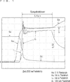
Zunächst wird das Problem genauer beschrieben, das während der Spiegelzeitdauer des Schaltelements auftritt. 1 ist ein Beispiel der Verhaltensweisen einer Gate-Emitter-Spannung VGE, einer Kollektor-Emitter-Spannung VCE, eines Kollektorstroms IC und einer Abtastspannung VS (die durch Umsetzen eines Abtaststroms, der durch ein Stromabtastelement eines IGBT geflossen ist, unter Verwendung eines Widerstandselements in eine Spannung erhalten wurde) zum Zeitpunkt des Einschaltens des mit einer induktiven Last verbundenen IGBT. In diesem Beispiel fließt durch einen IGBT mit einem Nennstrom von 300 A unmittelbar nach dem Einschalten ein Kollektorstrom IC von etwa 260 A.First, the problem that occurs during the mirror period of the switching element will be described in more detail. 1 is an example of the behaviors of a gate-emitter voltage V GE , a collector-emitter voltage V CE , a collector current I C and a sense voltage V S (which is converted by converting a sense current that has flowed through a current sensing element of an IGBT a resistance element was obtained in a voltage) at the time of turning on the IGBT connected to an inductive load. In this example, an IGBT with a nominal current of 300 A flows immediately after switching on a collector current I C of about 260 A.
Beim Anstieg eines in ein Gate des IGBT einzugebenden Ansteuersignals steigt die Gate-Emitter-Spannung VGE, um den IGBT einzuschalten, wobei es aber unmittelbar danach eine Zeitdauer gibt, in der die Gate-Emitter-Spannung VGE vorübergehend konstant ist. In 1 wird die Gate-Emitter-Spannung VGE unmittelbar nach dem Einschalten des IGBT während einer Zeitdauer von etwa 2,4 μs auf etwa 10,8 V gehalten. Diese Zeitdauer ist eine ”Spiegelzeitdauer”. In 1 ist zu sehen, dass die Abtastspannung VS nach dem Nachschwingen eine Größenordnung von 0,5 V erreicht und nach der Spiegelzeitdauer abnimmt, trotzdem der Kollektorstrom IC nach dem Nachschwingen unmittelbar nach dem Einschalten des IGBT nahezu konstant ist.Upon the rise of a drive signal to be input to a gate of the IGBT, the gate-emitter voltage V GE rises to turn on the IGBT, but immediately thereafter, there is a period in which the gate-emitter voltage V GE is temporarily constant. In 1 For example, the gate-emitter voltage V GE immediately after turning on the IGBT during a period of about 2.4 microseconds held about 10.8V. This period of time is a "mirror period". In 1 It can be seen that the sense voltage V S after the ringing reaches an order of 0.5 V and decreases after the mirror period, despite the fact that the collector current I C after ringing is almost constant immediately after the IGBT is turned on.
Dieser Anstieg der Abtastspannung VS erzeugt eine fehlerhafte Detektierung des Überstroms unmittelbar nach dem Einschalten des IGBT, was dazu führt, dass die Überstromschutzschaltung einen fehlerhaften Betrieb ausführt. Wenn in dem Beispiel ausThis rise of the sense voltage V S generates erroneous detection of the overcurrent immediately after the IGBT is turned on, resulting in the overcurrent protection circuit performing erroneous operation. If in the example off
1 ein Schwellenwert der Abtastspannung VS, bei dem die Überstromschutzschaltung einen Schutzbetrieb beginnt, nicht höher als 0,5 V eingestellt worden ist, beginnt die Überstromschutzschaltung mit dem Schutzbetrieb für den IGBT, trotzdem der Kollektorstrom IC höchstens gleich dem Nennstrom ist. 1 When a threshold value of the sense voltage V S at which the overcurrent protection circuit starts a protection operation has not been set higher than 0.5 V, the overcurrent protection circuit starts the protection operation for the IGBT, although the collector current I C is at most equal to the rated current.
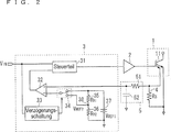
2 ist ein Stromlaufplan einer Halbleitervorrichtung in Übereinstimmung mit einer ersten bevorzugten Ausführungsform. Die Halbleitervorrichtung ist mit einem Schaltelement 1, mit einer Ansteuerschaltung 2, mit einer Überstromschutzschaltung 3, mit einem Abtastwiderstand 4 und mit einem Tiefpassfilter 5 versehen. 2 FIG. 10 is a circuit diagram of a semiconductor device in accordance with a first preferred embodiment. FIG. The semiconductor device is provided with a switching element 1 , with a drive circuit 2 , with an overcurrent protection circuit 3 , with a sense resistor 4 and with a low pass filter 5 Mistake.
In der derzeit bevorzugten Ausführungsform wird als das Schaltelement 1 ein IGBT 11 mit einem darin eingebauten Stromabtastelement verwendet. Durch einen Ausgangsanschluss (Abtastanschluss) des Stromabtastelements fließt ein Abtaststrom, der proportional zu einem Kollektorstrom (Hauptstrom) des IGBT 11 ist.In the presently preferred embodiment, as the switching element 1 an IGBT 11 used with a current sensing element incorporated therein. Through an output terminal (sense terminal) of the current sensing element, a sense current flows in proportion to a collector current (main current) of the IGBT 11 is.
Der Abtastwiderstand 4 ist zwischen den Abtastanschluss und einen Emitteranschluss des IGBT 11 geschaltet und ist ein passives Element, das einen Abtaststrom in eine Spannung (Abtastspannung) umsetzt. Es wird angemerkt, dass ein Widerstandswert RS des Abtastwiderstands 4 äquivalent dem eines Abtastwiderstands in einer herkömmlichen Halbleitervorrichtung ist.The sense resistor 4 is between the sense terminal and an emitter terminal of the IGBT 11 and is a passive element that converts a sense current into a voltage (sense voltage). It is noted that a resistance value R S of the sense resistor 4 equivalent to that of a sense resistor in a conventional semiconductor device.
Die Abtastspannung wird über ein Tiefpassfilter 5, das aus einem Widerstand 51 und aus einem Kondensator 52 besteht, in die Überstromschutzschaltung 3 eingegeben. Eine Zeitkonstante des Tiefpassfilters 5 ist wenigstens so groß wie ein Nachschwingzyklus, während sie ausreichend kürzer als die Spiegelzeitdauer des Schaltelements 1 ist und erwünscht ist, dass sie höchstens so groß wie die Hälfte der Spiegelzeitdauer ist. Genauer kann sie z. B. genauso lang wie die Erholungszeit für eine Freilaufdiode (nicht gezeigt) sein, die zusammen mit dem Schaltelement 1 verwendet wird. Um einen fehlerhaften Betrieb wegen des Nachschwingens zu verhindern, wird der Überstromschutzschaltung 3 eine Abtastspannung zugeführt, aus der das Nachschwingen durch das Tiefpassfilter 5 entfernt worden ist.The scanning voltage is via a low-pass filter 5 that comes from a resistance 51 and from a capacitor 52 exists in the overcurrent protection circuit 3 entered. A time constant of the low-pass filter 5 is at least as large as a ringing cycle while being sufficiently shorter than the mirror period of the switching element 1 is and is desired to be at most as large as half the mirror period. More precisely, she can z. B. as long as the recovery time for a freewheeling diode (not shown), which together with the switching element 1 is used. To prevent erroneous operation due to the ringing, the overcurrent protection circuit 3 supplied a scanning voltage, from which the ringing through the low-pass filter 5 has been removed.
Die Ansteuerschaltung 2 erzeugt auf der Grundlage eines Eingangssignals VIN als eines von außen einzugebenden Steuersignals ein Ansteuersignal, das in ein Gate des IGBT 11 eingegeben werden soll. Hier ist angenommen, dass das Schaltelement 1 in der Weise gesteuert wird, dass es eingeschaltet wird, wenn das Eingangssignal VIN auf einem H-Pegel ist, und ausgeschaltet wird, wenn das Eingangssignal VIN auf einem L-Pegel ist.The drive circuit 2 generates, on the basis of an input signal V IN as a control signal to be externally input, a drive signal which is input to a gate of the IGBT 11 should be entered. Here it is assumed that the switching element 1 is controlled so that it is turned on when the input signal V IN is at an H level, and is turned off when the input signal V IN is at an L level.
Das Eingangssignal VIN wird der Ansteuerschaltung 2 über die Überstromschutzschaltung 3 zugeführt. Die Überstromschutzschaltung 3 überwacht anhand der Abtastspannung einen über das Schaltelement 1 fließenden Hauptstrom und überträgt normalerweise das Eingangssignal VIN zu der Ansteuerschaltung 2. Wenn sie dagegen detektiert, dass über das Schaltelement 1 ein Überstrom geflossen ist (dass der Hauptstrom höher als die SC-Auslösestärke gewesen ist), hält die Überstromschutzschaltung 3 die Zufuhr des Eingangssignals VIN zu der Ansteuerschaltung 2 an, um einen vorgegebenen Schutzbetrieb wie etwa das Abschalten des Schaltelements 1 auszuführen.The input signal V IN becomes the drive circuit 2 via the overcurrent protection circuit 3 fed. The overcurrent protection circuit 3 monitored on the basis of the scanning voltage via the switching element 1 flowing main current and normally transmits the input signal V IN to the drive circuit 2 , If, on the other hand, it detects that via the switching element 1 an overcurrent has flowed (that the main current has been higher than the SC trip level), holds the overcurrent protection circuit 3 the supply of the input signal V IN to the drive circuit 2 to a predetermined protective operation such as switching off the switching element 1 perform.
Die Überstromschutzschaltung 3 ist durch einen Steuerteil 31, durch einen Komparator 32, durch eine Verzögerungsschaltung 33, durch einen Schalter 34, durch Widerstände 35 und 36 und durch eine Referenzspannungsquelle 37 konfiguriert. Eine Reihenschaltung der Widerstände 35 und 36 ist zu der Referenzspannungsquelle 37 parallelgeschaltet, und eine zweite Referenzspannung VREF2, die dadurch erhalten wird, dass die Widerstände 35 und 36 eine von der Referenzspannungsquelle 37 ausgegebene erste Referenzspannung VREF1 teilen, wird an einen Verbindungsknoten 38 zwischen den Widerständen 35 und 36 ausgegeben. Im Folgenden ist der Verbindungsknoten 38 zwischen den Widerständen 35 und 36 als ein ”Spannungsteiler-Referenzpunkt” bezeichnet.The overcurrent protection circuit 3 is through a control part 31 , through a comparator 32 , by a delay circuit 33 , by a switch 34 , by resistances 35 and 36 and by a reference voltage source 37 configured. A series connection of the resistors 35 and 36 is to the reference voltage source 37 connected in parallel, and a second reference voltage V REF2 , which is obtained by the resistors 35 and 36 one from the reference voltage source 37 outputted first reference voltage V REF1 is sent to a connection node 38 between the resistances 35 and 36 output. The following is the connection node 38 between the resistances 35 and 36 referred to as a "voltage divider reference point".
Eine Abtastspannung wird über das Tiefpassfilter 5 in einen nicht invertierenden Eingangsanschluss (positiven Anschluss (”+”- Anschluss)) des Komparators 32 eingegeben. Die Referenzspannungsquelle 37 oder der Spannungsteiler-Referenzpunkt 38 wird wahlweise mit einem invertierenden Eingangsanschluss (negativen Anschluss (”–”-Anschluss)) des Komparators 32 verbunden. Die von dem Spannungsteiler-Referenzpunkt 38 ausgegebene zweite Referenzspannung VREF2 wird durch Teilung der durch die Referenzspannungsquelle 37 ausgegebenen ersten Referenzspannung VREF1 in einem Spannungsteilungsverhältnis zwischen den Widerständen 35 und 36 erhalten, wobei die zweite Referenzspannung VREF2 somit niedriger als die erste Referenzspannung VREF1 ist. Die von dem Spannungsteiler-Referenzpunkt 38 ausgegebene zweite Referenzspannung VREF2 wird auf einen Wert einer Abtastspannung eingestellt, der zu dem Zeitpunkt erscheint, zu dem die Stärke des über das Schaltelement 1 fließenden Hauptstroms der SC-Auslösestärke entspricht (d. h., der Wert ist äquivalent einem Schwellenwert, mit dem eine Überstromschutzschaltung der herkömmlichen Halbleitervorrichtung den Schutzbetrieb beginnt). Die von der Referenzspannungsquelle 37 ausgegebene erste Referenzspannung VREF1 wird auf einen Wert einer Abtastspannung eingestellt, die zu dem Zeitpunkt erscheint, zu dem die Stärke des während der Spiegelzeitdauer über das Schaltelement 1 fließenden Hauptstroms der SC-Auslösestärke entspricht (d. h. auf einen Wert, der angesichts eines während der Spiegelzeitdauer in Bezug auf den Schwellenwert, mit dem die Überstromschutzschaltung der herkömmlichen Halbleitervorrichtung der Schutzbetrieb beginnt, erhöhten Abtaststroms (Stromteilungsverhältnis) erhöht ist).A scanning voltage is passed through the low-pass filter 5 into a non-inverting input terminal (positive terminal ("+" terminal)) of the comparator 32 entered. The reference voltage source 37 or the voltage divider reference point 38 is optionally provided with an inverting input terminal (negative terminal ("-" terminal)) of the comparator 32 connected. That of the voltage divider reference point 38 output second reference voltage V REF2 is divided by the by the reference voltage source 37 outputted first reference voltage V REF1 in a voltage dividing ratio between the resistors 35 and 36 Thus, the second reference voltage V REF2 is lower than the first reference voltage V REF1 . That of the voltage divider reference point 38 outputted second reference voltage V REF2 is set to a value of a sense voltage appearing at the time when the magnitude of the over the switching element 1 flowing SC current (that is, the value is equivalent to a threshold value at which an overcurrent protection circuit of the conventional semiconductor device starts the protection operation). The from the reference voltage source 37 output first reference voltage V REF1 is set to a value of a scanning voltage appearing at the time when the intensity of the same during the mirror period via the switching element 1 current peak current of the SC trigger strength (ie, increased to a value increased during the mirror period with respect to the threshold at which the overcurrent protection circuit of the conventional semiconductor device, the protection operation starts increased sense current (current division ratio)).
Das Schalten, ob der negative Anschluss des Komparators 32 mit der Referenzspannungsquelle 37 oder mit dem Spannungsteiler-Referenzpunkt 38 verbunden wird, wird durch den Schalter 34 ausgeführt, wobei sein Betrieb durch eine Verzögerungsschaltung 33 gesteuert wird. Die Verzögerungsschaltung 33 steuert den Schalter 34, um nur während einer Zeitdauer vom Anstieg des Eingangssignals VIN bis zum Verstreichen einer vorgegebenen Verzögerungszeit danach die Referenzspannungsquelle 37 mit dem negativen Anschluss des Komparators 32 zu verbinden und während der anderen Zeitdauern den Spannungsteiler-Referenzpunkt 38 mit dem negativen Anschluss des Komparators 32 zu verbinden.The switching, whether the negative terminal of the comparator 32 with the reference voltage source 37 or with the voltage divider reference point 38 is connected through the switch 34 executed, its operation by a delay circuit 33 is controlled. The delay circuit 33 controls the switch 34 for only the reference voltage source for a period of time from the rise of the input signal V IN until the lapse of a predetermined delay time thereafter 37 with the negative terminal of the comparator 32 and during the other periods, the voltage divider reference point 38 with the negative terminal of the comparator 32 connect to.
Die in der Verzögerungsschaltung 33 eingestellte Verzögerungszeit ist äquivalent oder wenigstens gleich der Länge der Spiegelzeitdauer des Schaltelements 1 eingestellt worden. In der derzeit bevorzugten Ausführungsform ist in der Verzögerungsschaltung 33 die der Spiegelzeitdauer äquivalente Verzögerungszeit eingestellt worden.The in the delay circuit 33 set delay time is equivalent or at least equal to the length of the mirror period of the switching element 1 been discontinued. In the presently preferred embodiment, in the delay circuit 33 the delay time equivalent to the mirror period has been set.
Eine Ausgabe des Komparators 32 ist auf einem L-Pegel (Tief-Pegel), wenn eine in den positiven Anschluss eingegebene Abtastspannung niedriger als die Spannung des negativen Anschlusses (die erste Referenzspannung VREF1 oder die zweite Referenzspannung VREF2) ist, während die Ausgabe auf einem H-Pegel (Hoch-Pegel) ist, wenn die Abtastspannung eine Spannung des negativen Anschlusses übersteigt. Die Ausgabe des Komparators 32 wird zum Steuern eines Betriebs des Steuerteils 31 verwendet.An output of the comparator 32 is at an L level (low level) when a sense voltage input to the positive terminal is lower than the voltage of the negative terminal (the first reference voltage V REF1 or the second reference voltage V REF2 ) while the output is at an H level (High level) when the sense voltage exceeds a voltage of the negative terminal. The output of the comparator 32 is used to control an operation of the control part 31 used.
Das Eingangssignal VIN wird in den Steuerteil 31 eingegeben. Der Steuerteil 31 sendet das Eingangssignal VIN zu der Ansteuerschaltung 2, wenn der Ausgang des Komparators 32 auf dem L-Pegel ist. Wenn die Ausgabe des Komparators 32 dagegen auf den H-Pegel übergeht, bestimmt der Steuerteil 31, dass ein Überstrom über das Schaltelement 1 geflossen ist, und gibt zu der Ansteuerschaltung 2 ein Signal zum Abschalten des Schaltelements 1 aus, um das Schaltelement 1 zu schützen.The input signal V IN is in the control part 31 entered. The control part 31 sends the input signal V IN to the drive circuit 2 when the output of the comparator 32 is at the L level. If the output of the comparator 32 on the other hand, goes to the H level, determines the control part 31 in that an overcurrent over the switching element 1 has flowed, and gives to the drive circuit 2 a signal for switching off the switching element 1 off to the switching element 1 to protect.
Wenn die Abtastspannung in der Halbleitervorrichtung aus 2 niedriger als eine Spannung des negativen Anschlusses des Komparators 32 ist, sendet der Steuerteil 31 in der Überstromschutzschaltung 3 das Eingangssignal VIN zu der Ansteuerschaltung 2, sodass das Schaltelement 1 in Übereinstimmung mit dem Eingangssignal VIN arbeitet. Ferner führt der Steuerteil 31 in der Überstromschutzschaltung 3 den Schutzbetrieb für das Schaltelement 1 aus, wenn die Abtastspannung wenigstens gleich der Spannung des negativen Anschlusses des Komparators 32 ist.When the scanning voltage in the semiconductor device is off 2 lower than a voltage of the negative terminal of the comparator 32 is, sends the control part 31 in the overcurrent protection circuit 3 the input signal V IN to the drive circuit 2 so that the switching element 1 operates in accordance with the input signal V IN . Furthermore, the control part leads 31 in the overcurrent protection circuit 3 the protective operation for the switching element 1 when the sense voltage is at least equal to the voltage of the negative terminal of the comparator 32 is.
Die Spannung des negativen Anschlusses des Komparators 32 dient als der Schwellenwert der Abtastspannung, mit dem die Überstromschutzschaltung 3 den Schutzbetrieb für das Schaltelement 1 beginnt, wobei der Schwellenwert aber durch den Schalter 34 geschaltet werden kann. Das heißt, der Schwellenwert ist während einer bestimmten Zeitdauer (die der in der Verzögerungsschaltung 33 eingestellten Verzögerungszeit entspricht) ab dem Anstieg des Eingangssignals VIN die erste Referenzspannung VREF1, während der Schwellenwert während der anderen Zeitdauern die zweite Referenzspannung VREF2 ist.The voltage of the negative terminal of the comparator 32 serves as the threshold of the sense voltage with which the overcurrent protection circuit 3 the protective operation for the switching element 1 starts, but the threshold is set by the switch 34 can be switched. That is, the threshold is during a certain period of time (that in the delay circuit 33 adjusted delay time) from the rise of the input signal V IN, the first reference voltage V REF1 , while the threshold during the other periods, the second reference voltage V REF2 .
In der derzeit bevorzugten Ausführungsform ist die zweite Referenzspannung VREF2 niedriger als die erste Referenzspannung VREF1 eingestellt worden und ist die Verzögerungszeit der Verzögerungsschaltung 33 äquivalent der Länge der Spiegelzeitdauer des Schaltelements 1 eingestellt worden. Somit wird der Schwellenwert der Abtastspannung, mit dem die Überstromschutzschaltung 3 den Schutzbetrieb für das Schaltelement 1 beginnt, in der Halbleitervorrichtung aus 2 nur während der Spiegelzeitdauer unmittelbar nach Einschalten des Halbleiterelements 1 hoch eingestellt.In the currently preferred embodiment, the second reference voltage V REF2 has been set lower than the first reference voltage V REF1 and is the delay time of the delay circuit 33 equivalent to the length of the mirror period of the switching element 1 been discontinued. Thus, the threshold of the scanning voltage with which the overcurrent protection circuit 3 the protective operation for the switching element 1 begins in the semiconductor device 2 only during the mirror period immediately after switching on the semiconductor element 1 set high.
Folglich wird während der Spiegelzeitdauern des Schaltelements 1 verhindert, dass die Abtastspannung den Schwellenwert erreicht, bei dem die Überstromschutzschaltung 3 den Schutzbetrieb beginnt. Dementsprechend kann ein fehlerhafter Betrieb der Überstromschaltung 3 selbst dann verhindert werden, wenn sich das Stromteilungsverhältnis des Abtaststroms zu dem Hauptstrom in dem Schaltelement 1 während der Spiegelzeitdauer ändert und die Abtastspannung steigt.Consequently, during the mirror periods of the switching element 1 prevents the sense voltage from reaching the threshold at which the overcurrent protection circuit 3 the protective operation begins. Accordingly, erroneous operation of the overcurrent circuit 3 even if the current dividing ratio of the sense current to the main current in the switching element 1 during the mirror period changes and the scanning voltage increases.
Wenn der IGBT 11, der das Schaltelement 1 bildet, zum Zeitpunkt des Einschaltens z. B. ein in 1 gezeigtes Verhalten annimmt, wird die erste Referenzspannung VREF1 auf 0,7 V eingestellt, wird die zweite Referenzspannung VREF2 auf 0,5 V eingestellt und wird die Verzögerungszeit der Verzögerungsschaltung 33 auf wenigstens 2,4 μs eingestellt. In diesem Fall ist der Schwellenwert der Abtastspannung, mit dem die Überstromschutzschaltung 3 den Schutzbetrieb beginnt, während der Spiegelzeitdauer des Schaltelements 1 0,7 V, d. h. höher als im Fall der herkömmlichen Halbleitervorrichtung, sodass ein fehlerhafter Betrieb der Überstromschutzschaltung 3 verhindert wird. Darüber hinaus kann der Schutzbetrieb mit dem der ersten Referenzspannung VREF1 entsprechenden Schwellenwert während der Spiegelzeitdauer ebenfalls ausgeführt werden.If the IGBT 11 that the switching element 1 forms, at the time of switching z. B. in 1 assumes the first reference voltage V REF1 is set to 0.7 V, the second reference voltage V REF2 is set to 0.5 V and becomes the delay time of the delay circuit 33 set to at least 2.4 μs. In this case, the threshold value of the scanning voltage with which the overcurrent protection circuit 3 the protection operation starts during the mirror period of the switching element 1 0.7 V, that is higher than in the case of the conventional semiconductor device, so that erroneous operation of the overcurrent protection circuit 3 is prevented. In addition, the protection operation at the threshold corresponding to the first reference voltage V REF1 may also be performed during the mirror period.
Wenn die Spiegelzeitdauer abgeschlossen ist und das Schaltelement 1 in den stationären Zustand gelangt, nimmt sein Schwellenwert ferner auf 0,5 V ab, was äquivalent dem Fall der herkömmlichen Halbleitervorrichtung ist, wodurch ein ähnlicher Schutzbetrieb wie herkömmlich ausgeführt werden kann.When the mirror time is complete and the switching element 1 goes to the steady state, its threshold further decreases to 0.5V, which is equivalent to the case of the conventional semiconductor device, whereby a similar protection operation can be carried out as conventionally.
In der Halbleitervorrichtung der derzeit bevorzugten Ausführungsform wird die Zeitkonstante des Tiefpassfilters 5 ausreichend kürzer als die Länge der Spiegelzeitdauer eingestellt und wird das Verfahren zum Maskieren der in die Überstromschutzschaltung 3 einzugebenden Abtastspannung während der Spiegelzeitdauer nicht verwendet, wodurch das Auftreten einer Verzögerung in dem Betrieb der Überstromschutzschaltung 3 verhindert wird. Ferner ist in der gebildeten Konfiguration nur die einzelne Referenzspannungsquelle 37 vorgesehen, deren Spannung geteilt wird, wodurch die Notwendigkeit mehrerer Referenzspannungsquellen beseitigt wird und die Schaltung vereinfacht werden kann.In the semiconductor device of the presently preferred embodiment, the time constant of the low-pass filter becomes 5 is set sufficiently shorter than the length of the mirror period, and the method for masking in the overcurrent protection circuit 3 is not used during the mirror period, whereby the occurrence of a delay in the operation of the overcurrent protection circuit 3 is prevented. Furthermore, in the configuration formed, only the single reference voltage source is used 37 whose voltage is shared, eliminating the need for multiple reference voltage sources and simplifying the circuit.
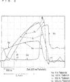
3 zeigt ein Beispiel der Verhaltensweisen einer Gate-Emitter-Spannung VGE, einer Kollektor-Emitter-Spannung VCE, eines Kollektorstroms IC und einer Abtastspannung VS in dem IGBT zum Zeitpunkt der Brückenschaltung desselben IGBT (Nennstrom 300 A), wie er für die Messung aus 1 verwendet worden ist, und des gleichzeitigen Einschaltens des oberen Zweigs und des unteren Zweigs des IGBT, um (in dem oberen und in dem unteren Zweig) einen Kurzschluss zu erzeugen. Mit einer Zunahme des Kollektorstroms IC nimmt die Abtastspannung Vs bis auf maximal 3,5 V zu. 3 shows an example of the behaviors of a gate-emitter voltage V GE , a collector-emitter voltage V CE , a collector current I C and a sense voltage V S in the IGBT at the time of the bridge connection of the same IGBT (rated current 300 A) as used for the measurement off 1 and simultaneously turning on the upper branch and lower branch of the IGBT to short-circuit (in the upper and lower branches). As the collector current I C increases, the sense voltage Vs increases to a maximum of 3.5V.
3 ist ein Beispiel dafür, dass ein Mittel zum Maskieren der in die Überstromschutzschaltung einzugebenden Abtastspannung während der Spiegelzeitdauer (2,4 μs) verwendet wird, wobei auch dann, wenn in dem oberen und in dem unteren Zweig ein Kurzschluss auftritt, da der IGBT eingeschaltet wird und ein Überstrom fließt, eine Verzögerung von 2,4 μs auftritt, bis die Überstromschutzschaltung mit dem Schutzbetrieb beginnt. 3 is an example of that means for masking the sense voltage to be input to the overcurrent protection circuit is used during the mirror period (2.4 μs), even if a short circuit occurs in the upper and lower branches because the IGBT is turned on and an overcurrent flows, a delay of 2.4 μs occurs until the overcurrent protection circuit starts the protection operation.
Im Gegensatz dazu kann in der Halbleitervorrichtung der derzeit bevorzugten Ausführungsform ein Überstromschutzbetrieb mittels der Abtastspannung weiter ausgeführt, obgleich der Schwellenwert der Abtastspannung, mit dem die Überstromschutzschaltung 3 den Schutzbetrieb auszuführen beginnt, während der Spiegelzeitdauer hoch ist. Wenn in dem Beispiel aus 3 die Konfiguration der Halbleitervorrichtung der derzeit bevorzugten Ausführungsform angenommen worden ist und die erste Referenzspannung VREF1 auf 0,7 V eingestellt worden ist, erfolgt die Detektierung des Überstroms durch die Überstromschutzschaltung 3 800 ns nach Einschalten des IGBT (Beginn des Kurzschlusses in den Zweigen). Zu diesem Zeitpunkt wird der Schutzbetrieb begonnen und ist das Schaltelement 1 vor einer wesentlichen Zunahme des Kollektorstroms IC geschützt. Das heißt, im Vergleich zu dem Mittel zum Maskieren der Abtastspannung kann die Zeitdauer, bis der Schutzbetrieb ausgeführt wird, um 1,6 μs verringert werden, sodass der über das Schaltelement 1 fließende Überstrom unterdrückt werden kann, das die Schutzeigenschaften des Schaltelements 1 erheblich verbessert.In contrast, in the semiconductor device of the presently preferred embodiment, overcurrent protection operation can be further performed by means of the sense voltage, although the threshold value of the sense voltage with which the overcurrent protection circuit 3 start the protection operation while the mirror time is high. If in the example off 3 the configuration of the semiconductor device of the presently preferred embodiment has been adopted and the first reference voltage V REF1 has been set to 0.7 V, the overcurrent protection is detected by the overcurrent protection circuit 3 800 ns after switching on the IGBT (start of short circuit in the branches). At this time, the protection operation is started and is the switching element 1 protected against a substantial increase in the collector current I C. That is, as compared with the means for masking the sense voltage, the time until the protection operation is performed can be reduced by 1.6 μs, so that the time through the switching element 1 flowing overcurrent can be suppressed, the protective properties of the switching element 1 significantly improved.
Es wird angemerkt, dass das Schaltelement 1 nicht auf den IGBT beschränkt ist, sondern ein Schaltelement mit einer Spiegelzeitdauer wie etwa ein MOSFET sein kann. Ferner ist das Schaltelement 1 nicht auf ein unter Verwendung von Silicium (Si) Gebildetes beschränkt, sondern kann z. B. unter Verwendung eines Halbleiters mit breiter Bandlücke aus einem Material auf Siliciumnitridgrundlage (SiC), aus einem Material auf Galliumnitridgrundlage (GaN) oder aus Diamant gebildet sein. Die Verwendung des Schaltelements unter Verwendung des Halbleiters mit breiter Bandlücke kann eine hohe Spannungsfestigkeit, einen niedrigen Verlust und eine hohe Wärmebeständigkeit der Halbleitervorrichtung verwirklichen.It is noted that the switching element 1 is not limited to the IGBT, but may be a switching element having a mirror period such as a MOSFET. Furthermore, the switching element 1 not limited to one formed by using silicon (Si), but may be e.g. Example, using a wide bandgap semiconductor of a silicon nitride-based material (SiC), a gallium nitride based material (GaN) or diamond may be formed. The use of the switching element using the wide bandgap semiconductor can realize high withstand voltage, low loss, and high heat resistance of the semiconductor device.
Zweite bevorzugte AusführungsformSecond preferred embodiment
4 ist ein Stromlaufplan einer Halbleitervorrichtung in Übereinstimmung mit der zweiten bevorzugten Ausführungsform. In 4 sind Elemente mit einer ähnlichen Funktion wie in 2 gezeigte mit denselben Bezugszeichen bezeichnet. 4 FIG. 12 is a circuit diagram of a semiconductor device in accordance with the second preferred embodiment. FIG. In 4 are elements with a similar function as in 2 indicated by the same reference numerals.
In der derzeit bevorzugten Ausführungsform ist der negative Anschluss des Komparators 32 in der Überstromschutzschaltung 3 mit der Referenzspannungsquelle 37 verbunden, die die Referenzspannung VREF ausgibt. Das heißt, der Schwellenwert, mit dem die Überstromschutzschaltung 3 den Schutzbetrieb beginnt, ist auf die Referenzspannung VREF festgesetzt. Ein Wert einer Referenzspannung VREF ist auf einen Wert einer Abtastspannung gesetzt, die zu dem Zeitpunkt erscheint, zu dem der der SC-Auslösestärke entsprechende Hauptstrom über das Schaltelement 1 fließt (d. h. auf einen Wert, der äquivalent einem Schwellenwert ist, mit dem die Überstromschutzschaltung der herkömmlichen Halbleitervorrichtung den Schutzbetrieb beginnt).In the currently preferred embodiment, the negative terminal is the comparator 32 in the overcurrent protection circuit 3 with the reference voltage source 37 connected, which outputs the reference voltage V REF . That is, the threshold, with the overcurrent protection circuit 3 the protective operation begins, is set to the reference voltage V REF . A value of a reference voltage V REF is set to a value of a sense voltage appearing at the time when the main current corresponding to the SC trigger strength is supplied through the switching element 1 flows (ie, to a value equivalent to a threshold value at which the overcurrent protection circuit of the conventional semiconductor device starts the protection operation).
Als der Abtastwiderstand, der mit dem Abtastanschluss des IGBT 11 zu verbinden ist, ist eine Reihenschaltung der Widerstände 41 und 42 verwendet. Eine Summe eines Widerstandswerts RS1 des Widerstands 41 und eines Widerstandswerts RS2 des Widerstands 42 ist äquivalent dem des Abtastwiderstands in der herkömmlichen Halbleitervorrichtung eingestellt worden. Ferner ist der Widerstand 42 zu einem Schalter 6 parallelgeschaltet und ist der Widerstand 42 so konfiguriert, dass die beiden Anschlüsse des Widerstands 42 kurzgeschlossen werden, wenn der Schalter 6 eingeschaltet wird.As the sense resistor connected to the sense terminal of the IGBT 11 to connect is a series connection of the resistors 41 and 42 used. A sum of a resistance R S1 of the resistor 41 and a resistance value R S2 of the resistor 42 has been set equivalent to that of the sampling resistor in the conventional semiconductor device. Further, the resistance 42 to a switch 6 connected in parallel and is the resistor 42 configured so that the two connections of the resistor 42 be shorted when the switch 6 is turned on.
Ein Betrieb des Schalters 6 wird durch die Verzögerungsschaltung 33 gesteuert. Die Verzögerungsschaltung 33 schaltet den Schalter 6 während der Zeitdauer vom Anstieg des Eingangssignals VIN bis zum Verstreichen der vorgegebenen Verzögerungszeit danach ein, während sie den Schalter 6 während der anderen Zeitdauern ausschaltet. Die in der Verzögerungsschaltung 33 eingestellte Verzögerungszeit ist äquivalent oder wenigstens gleich der Länge der Spiegelzeitdauer des Schaltelements 1 eingestellt worden. In der Verzögerungsschaltung 33 in der derzeit bevorzugten Ausführungsform ist die Verzögerungszeit äquivalent der Spiegelzeitdauer eingestellt worden.An operation of the switch 6 is through the delay circuit 33 controlled. The delay circuit 33 turns on the switch 6 during the period from the rise of the input signal V IN until the lapse of the predetermined delay time thereafter, while the switch 6 during the other periods of time off. The in the delay circuit 33 set delay time is equivalent or at least equal to the length of the mirror period of the switching element 1 been discontinued. In the delay circuit 33 In the presently preferred embodiment, the delay time has been set equivalent to the mirror duration.
Wenn in der Halbleitervorrichtung aus 4 die in den positiven Anschluss des Komparators 32 einzugebende Abtastspannung niedriger als die Referenzspannung VREF ist, sendet der Steuerteil 31 in der Überstromschutzschaltung 3 das Eingangssignal VIN zu der Ansteuerschaltung 2 und arbeitet das Schaltelement 1 in Übereinstimmung mit dem Eingangssignal VIN. Ferner führt der Steuerteil 31 in der Überstromschutzschaltung 3 den Schutzbetrieb für das Schaltelement 1 aus, wenn die Abtastspaltung wenigstens gleich der Referenzspannung VREF ist.When in the semiconductor device 4 which in the positive terminal of the comparator 32 to be inputted scanning voltage is lower than the reference voltage V REF , sends the control part 31 in the overcurrent protection circuit 3 the input signal V IN to the drive circuit 2 and works the switching element 1 in accordance with the input signal V IN . Furthermore, the control part leads 31 in the overcurrent protection circuit 3 the protective operation for the switching element 1 when the scanning gap is at least equal to the reference voltage V REF .
In der Halbleitervorrichtung aus 4 wird der Widerstandswert des Abtastwiderstands zum Erzeugen der in den positiven Anschluss des Komparators 32 einzugebenden Abtastspannung durch den Schalter 6 geschaltet. Das heißt, da der Schalter 6 während einer bestimmten Zeitdauer (die der in der Verzögerungsschaltung 33 eingestellten Verzögerungszeit entspricht) nach dem Anstieg des Eingangssignals VIN eingeschaltet wird, ist der Abtastwiderstand nur der Widerstand 41 und sein Widerstandswert Rs1. Andererseits ist der Schalter 6 während der anderen Zeitdauern eingeschaltet, sodass der Abtastwiderstand als eine Reihenschaltung der Widerstände 41 und 42 dient und sein Widerstandswert RS1 + RS2 ist.In the semiconductor device 4 is the resistance of the sample resistor for generating the in the positive terminal of the comparator 32 to be entered scanning voltage through the switch 6 connected. That is, because the switch 6 during a certain period of time (that in the delay circuit 33 set delay time) is turned on after the rise of the input signal V IN , the sense resistor is only the resistor 41 and its resistance R s1 . On the other hand, the switch 6 during the other periods, so that the sense resistor acts as a series connection of the resistors 41 and 42 is and its resistance R S1 + R S2 is.
In der derzeit bevorzugten Ausführungsform ist die Verzögerungszeit der Verzögerungsschaltung 33 äquivalent der Länge der Spiegelzeitdauer des Schaltelements 1 eingestellt worden, sodass der Widerstandswert des Abtastwiderstands in der Halbleitervorrichtung aus 4 nur während der Spiegelzeitdauer unmittelbar nach Einschalten des Schaltelements 1 kleiner als im Fall der herkömmlichen Halbleitervorrichtung eingestellt wird. Die Konfiguration ist derart, dass der Widerstand 42 durch den Schalter 6 kurzgeschlossen ist, sodass der Widerstandswert des Abtastwiderstands selbst während eines Übergangsbetriebs, während der Schalter 6 ein- oder ausgeschaltet wird, nicht instabil wird, sodass die Überstromschutzschaltung 3 einen stabilen Schutzbetrieb ausführen kann.In the currently preferred embodiment, the delay time is the delay circuit 33 equivalent to the length of the mirror period of the switching element 1 has been set so that the resistance of the sense resistor in the semiconductor device 4 only during the mirror period immediately after switching on the switching element 1 is set smaller than in the case of the conventional semiconductor device. The configuration is such that the resistance 42 through the switch 6 is shorted so that the resistance of the sense resistor itself during a transient operation while the switch 6 is switched on or off, does not become unstable, so the overcurrent protection circuit 3 can perform a stable protection operation.
Dementsprechend können die Zunahmen der Abtastspannung selbst dann unterdrückt werden, wenn das Stromteilungsverhältnis des Abtaststroms zu dem Hauptstrom in dem Schaltelement 1 während der Spiegelzeitdauer schwankt und die Abtastspannung zunimmt. Das heißt, es wird verhindert, dass die Abtastspannung während der Spiegelzeitdauer den Schwellenwert erreicht, mit dem die Überstromschutzschaltung 3 den Schutzbetrieb beginnt, sodass der fehlerhafte Betrieb der Überstromschutzschaltung 3 verhindert werden kann.Accordingly, the increases of the scanning voltage can be suppressed even when the current dividing ratio of the sense current to the main current in the switching element 1 during the mirror period varies and the scanning voltage increases. That is, the sense voltage during the mirror period is prevented from reaching the threshold at which the overcurrent protection circuit 3 the protective operation starts, so that the erroneous operation of the overcurrent protection circuit 3 can be prevented.
Ferner wird der Widerstandswert des Abtastwiderstands äquivalent dem Fall der herkömmlichen Halbleitervorrichtung, wenn die Spiegelzeitdauer abgeschlossen ist und das Schaltelement 1 in den stationären Zustand gelangt, wodurch ein ähnlicher Schutzbetrieb wie herkömmlich ausgeführt werden kann.Further, the resistance value of the sense resistor becomes equivalent to the case of the conventional semiconductor device when the mirror period is completed and the switching element 1 enters the steady state, whereby a similar protection operation can be carried out as conventional.
Auch in der Halbleitervorrichtung der derzeit bevorzugten Ausführungsform ist die Zeitkonstante des Tiefpassfilters 5 ausreichend kürzer als die Länge der Spiegelzeitdauer eingestellt worden, wobei das Verfahren zum Maskieren der in die Überstromschutzschaltung 3 einzugebenden Abtastspannung während der Spiegelzeitdauer nicht verwendet wird, wodurch das Auftreten einer Verzögerung im Betrieb der Überstromschutzschaltung 3 verhindert wird.Also in the semiconductor device of the presently preferred embodiment is the time constant of the low-pass filter 5 sufficiently shorter than the length of the mirror period, the method of masking the overcurrent protection circuit 3 to be inputted during the mirror period is not used, whereby the occurrence of a delay in the operation of the overcurrent protection circuit 3 is prevented.
Obgleich der Schalter 6 zu dem Widerstand 42 in 4 parallelgeschaltet ist, kann außerdem eine ähnliche Wirkung erhalten werden, selbst wenn der Schalter 6 zu dem Widerstand 41 in Reihe geschaltet ist.Although the switch 6 to the resistance 42 in 4 In addition, a similar effect can be obtained even if the switch 6 to the resistance 41 is connected in series.
Dritte bevorzugte Ausführungsform Third preferred embodiment
5 ist ein Stromlaufplan einer Halbleitervorrichtung in Übereinstimmung mit einer dritten bevorzugten Ausführungsform. 5 FIG. 12 is a circuit diagram of a semiconductor device in accordance with a third preferred embodiment. FIG.
Eine Konfiguration der Halbleitervorrichtung ist dadurch gebildet, dass anstelle des Schalters 6 in der Konfiguration aus 4 ein Kondensator 7 zu dem Widerstand 42 parallelgeschaltet ist und dass die Verzögerungsschaltung 33 daraus weggelassen ist.A configuration of the semiconductor device is formed by replacing the switch 6 in the configuration 4 a capacitor 7 to the resistance 42 is in parallel and that the delay circuit 33 is omitted from it.
Eine Zeitkonstante einer durch die Widerstände 41 und 42 und durch den Kondensator 7 gebildeten Schaltung ist äquivalent oder wenigstens gleich der Spiegelzeitdauer des Schaltelements 1 eingestellt worden. In der derzeit bevorzugten Ausführungsform ist die Zeitkonstante äquivalent der Länge der Spiegelzeitdauer eingestellt worden.A time constant one through the resistors 41 and 42 and through the capacitor 7 The circuit formed is equivalent or at least equal to the mirror duration of the switching element 1 been discontinued. In the presently preferred embodiment, the time constant has been set equivalent to the length of the mirror period.
Ähnlich der zweiten bevorzugten Ausführungsform gelangt der Kondensator 7 in der Halbleitervorrichtung aus 5 nur während der Spiegelzeitdauer unmittelbar nach Einschalten des Schaltelements 1 in einen Kurzschlusszustand, sodass der Widerstandswert des Abtastwiderstands ein kleinerer Wert (Rs1) als im Fall der herkömmlichen Halbleitervorrichtung ist.Similar to the second preferred embodiment, the capacitor passes 7 in the semiconductor device 5 only during the mirror period immediately after switching on the switching element 1 in a short-circuited state such that the resistance value of the sense resistor is a smaller value (R s1 ) than in the case of the conventional semiconductor device.
Dementsprechend kann die Zunahme der Abtastspannung selbst dann unterdrückt werden, wenn das Stromteilungsverhältnis des Abtaststroms zu dem Hauptstrom in dem Schaltelement 1 während der Spiegelzeitdauer schwankt und die Abtastspannung zunimmt. Das heißt, es wird verhindert, dass die Abtastspannung während der Spiegelzeitdauer den Schwellenwert erreicht, mit dem die Überstromschutzschaltung 3 den Schutzbetrieb beginnt, sodass der fehlerhafte Betrieb der Überstromschutzschaltung 3 verhindert werden kann. Selbst während der Spiegelzeitdauer kann ein Schutzbetrieb ausgeführt werden, der dem Fall entspricht, dass der Widerstandswert des Abtastwiderstands Rs1 ist.Accordingly, the increase of the scanning voltage can be suppressed even if the current dividing ratio of the sense current to the main current in the switching element 1 during the mirror period varies and the scanning voltage increases. That is, the sense voltage during the mirror period is prevented from reaching the threshold at which the overcurrent protection circuit 3 the protective operation starts, so that the erroneous operation of the overcurrent protection circuit 3 can be prevented. Even during the mirror period, a protection operation corresponding to the case that the resistance value of the sense resistor R s1 is executed.
Ferner wird der Widerstandswert des Abtastwiderstands zu einem Wert (Rs1 + Rs2), der äquivalent dem im Fall der herkömmlichen Halbleitervorrichtung ist, wenn die Spiegelzeitdauer abgeschlossen ist und das Schaltelement 1 in den stationären Zustand gelangt, wodurch ein ähnlicher Schutzbetrieb wie herkömmlich ausgeführt werden kann.Further, the resistance value of the sense resistor becomes a value (R s1 + R s2 ) which is equivalent to that in the case of the conventional semiconductor device when the mirror period is completed and the switching element 1 enters the steady state, whereby a similar protection operation can be carried out as conventional.
Außerdem ist in der Halbleitervorrichtung der derzeit bevorzugten Ausführungsform die Zeitkonstante des Tiefpassfilters 5 ausreichend kürzer als die Länge der Spiegelzeitdauer eingestellt und wird das Verfahren zum Maskieren der in die Überstromschutzschaltung 3 einzugebenden Abtastspannung während der Spiegelzeitdauer nicht verwendet, wodurch das Auftreten einer Verzögerung im Betrieb der Überstromschutzschaltung 3 verhindert wird.In addition, in the semiconductor device of the presently preferred embodiment, the time constant of the low-pass filter is 5 is set sufficiently shorter than the length of the mirror period, and the method for masking in the overcurrent protection circuit 3 is not used during the mirror period, whereby the occurrence of a delay in the operation of the overcurrent protection circuit 3 is prevented.
Vierte bevorzugte AusführungsformFourth preferred embodiment
In der zweiten und dritten bevorzugten Ausführungsform wird der Widerstandswert des Abtastwiderstands während der Spiegelzeitdauer des Schaltelements 1 verringert, um die in die Überstromschutzschaltung 3 einzugebende Abtastspannung zu verringern, um den fehlerhaften Betrieb der Überstromschutzschaltung 3 zu verhindern, wobei aber eine ähnliche Wirkung auch mit anderen Mitteln erhalten werden kann, die die Abtastspannung während der Spiegelzeitdauer verringern.In the second and third preferred embodiments, the resistance value of the sense resistor becomes the mirror period of the switching element 1 reduced to the in the overcurrent protection circuit 3 to reduce the scanning voltage to be input to the erroneous operation of the overcurrent protection circuit 3 but a similar effect can also be obtained by other means which reduce the scanning voltage during the mirror period.
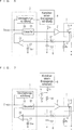
6 ist ein Stromlaufplan einer Halbleitervorrichtung in Übereinstimmung mit einer vierten bevorzugten Ausführungsform. Der Abtastwiderstand der Halbleitervorrichtung ist ein Abtastwiderstand 4 wie in der ersten bevorzugten Ausführungsform (2). Ferner ist eine Konfiguration der Überstromschutzschaltung 3 ähnlich der in der zweiten bevorzugten Ausführungsform (4). Darüber hinaus ist in der Halbleitervorrichtung der derzeit bevorzugten Ausführungsform an einem Ende des Abtastwiderstands 4 eine Korrekturstrom-Erzeugungsschaltung 8 vorgesehen, die den Korrekturstrom IA zum Vorspannen des Abtaststroms zuführt, wobei ein Betrag eines Korrekturstroms IA durch die Verzögerungsschaltung 33 in der Überstromschutzschaltung 3 gesteuert wird. 6 FIG. 12 is a circuit diagram of a semiconductor device in accordance with a fourth preferred embodiment. FIG. The sense resistor of the semiconductor device is a sense resistor 4 as in the first preferred embodiment ( 2 ). Further, a configuration of the overcurrent protection circuit 3 similar to that in the second preferred embodiment ( 4 ). Moreover, in the semiconductor device of the presently preferred embodiment, at one end of the sense resistor 4 a correction current generation circuit 8th provided, which supplies the correction current I A for biasing the sense current, wherein an amount of a correction current I A by the delay circuit 33 in the overcurrent protection circuit 3 is controlled.
Die Verzögerungsschaltung 33 verringert nur während der Zeitdauer ab dem Anstieg des Eingangssignals VIN bis zum Verstreichen einer vorgegebenen Zeitverzögerung danach den durch die Korrekturstrom-Erzeugungsschaltung 8 dem Abtastwiderstand 4 zuzuführenden Korrekturstrom IA. In der Verzögerungsschaltung 33 ist die Verzögerungszeit äquivalent oder wenigstens gleich der Länge der Spiegelzeitdauer des Schaltelements 1 eingestellt worden.The delay circuit 33 Only during the period of time from the rise of the input signal V IN until the lapse of a predetermined time delay thereafter, the current through the correction current generation circuit decreases 8th the sense resistor 4 to be supplied correction current I A. In the delay circuit 33 the delay time is equivalent or at least equal to the length of the mirror period of the switching element 1 been discontinued.
In der Verzögerungsschaltung 33 in der derzeit bevorzugten Ausführungsform ist die Verzögerungszeit äquivalent der Spiegelzeitdauer eingestellt worden. Ferner ist der Widerstandswert RS des Abtastwiderstands 4 derart eingestellt worden, dass die in den positiven Anschluss des Komparators 32 einzugebende Abtastspannung äquivalent der Referenzspannung VREF ist, wenn in dem Zustand, in dem der Korrekturstrom IA groß ist, über den IGBT 11 der Hauptstrom fließt, dessen Stärke der SC-Auslösestärke entspricht.In the delay circuit 33 In the presently preferred embodiment, the delay time has been set equivalent to the mirror duration. Further, the resistance R S of the sense resistor 4 have been adjusted so that in the positive terminal of the comparator 32 the sense voltage to be input is equivalent to the reference voltage V REF when, in the state in which the correction current I A is large, via the IGBT 11 the main current flows whose magnitude corresponds to the SC trigger strength.
In der Halbleitervorrichtung aus 6 ändert sich der Betrag der in den positiven Anschluss des Komparators 32 einzugebenden Abtastspannung in Übereinstimmung mit dem Betrag des Korrekturstroms IA. Das heißt, während der bestimmten Zeitdauer ab dem Anstieg des Eingangssignals VIN (die der in der Verzögerungsschaltung 33 eingestellten Verzögerungszeit entspricht), ist die Abtastspannung klein, da der Korrekturstrom IA klein ist. Andererseits ist die Abtastspannung während der anderen Zeitdauern groß, da der Korrekturstrom IA groß ist.In the semiconductor device 6 the amount changes into the positive terminal of the comparator 32 to be input scanning voltage in accordance with the amount of Correction current I A. That is, during the certain period of time from the rise of the input signal V IN (that of the delay circuit 33 set delay time), the sense voltage is small since the correction current I A is small. On the other hand, the sampling voltage during the other periods is large because the correction current I A is large.
In der derzeit bevorzugten Ausführungsform ist die Verzögerungszeit der Verzögerungsschaltung 33 äquivalent der Länge der Spiegelzeitdauer des Schaltelements 1 eingestellt worden, sodass die Abtastspannung in der Halbleitervorrichtung aus 6 nur während der Spiegelzeitdauer unmittelbar nach Einschalten des Schaltelements 1 unterdrückt wird.In the currently preferred embodiment, the delay time is the delay circuit 33 equivalent to the length of the mirror period of the switching element 1 is set so that the sense voltage in the semiconductor device 6 only during the mirror period immediately after switching on the switching element 1 is suppressed.
Dementsprechend können die Zunahmen der Abtastspannung selbst dann unterdrückt werden, wenn das Stromteilungsverhältnis des Abtaststroms zu dem Hauptstrom in dem Schaltelement 1 während der Spiegelzeitdauer schwankt und die Abtastspannung zunimmt. Das heißt, während der Spiegelzeitdauer wird verhindert, dass die Abtastspannung den Schwellenwert erreicht, mit dem die Überstromschutzschaltung 3 den Schutzbetrieb beginnt, sodass der fehlerhafte Betrieb der Überstromschutzschaltung 3 verhindert werden kann.Accordingly, the increases of the scanning voltage can be suppressed even when the current dividing ratio of the sense current to the main current in the switching element 1 during the mirror period varies and the scanning voltage increases. That is, during the mirror period, the sense voltage is prevented from reaching the threshold at which the overcurrent protection circuit 3 the protective operation starts, so that the erroneous operation of the overcurrent protection circuit 3 can be prevented.
Ferner wird die Abtastspannung groß, wenn die Spiegelzeitdauer abgeschlossen ist und das Schaltelement 1 in den stationären Zustand gelangt, wodurch ein ähnlicher Schutzbetrieb wie herkömmlich ausgeführt werden kann.Further, the scanning voltage becomes large when the mirror period is completed and the switching element 1 enters the steady state, whereby a similar protection operation can be carried out as conventional.
Außerdem ist die Zeitkonstante des Tiefpassfilters 5 in der Halbleitervorrichtung der derzeit bevorzugten Ausführungsform ebenfalls ausreichend kürzer als die Länge der Spiegelzeitdauer eingestellt worden und wird das Verfahren zum Maskieren der in die Überstromschutzschaltung 3 einzugebenden Abtastspannung während der Spiegelzeitdauer nicht verwendet, wodurch das Auftreten einer Verzögerung im Betrieb der Überstromschutzschaltung 3 verhindert wird.In addition, the time constant of the low-pass filter 5 in the semiconductor device of the presently preferred embodiment has also been set sufficiently shorter than the length of the mirror period, and the method for masking in the overcurrent protection circuit 3 is not used during the mirror period, whereby the occurrence of a delay in the operation of the overcurrent protection circuit 3 is prevented.
Obgleich eine Flussrichtung des Korrekturstroms IA in der obigen Beschreibung eine Richtung von der Korrekturstrom-Erzeugungsschaltung 8 zu dem Abtastwiderstand 4 (in Richtung eines Pfeils in 6) ist, wird angemerkt, dass sie eine umgekehrte Richtung sein kann. Wenn der Korrekturstrom IA von dem Abtastwiderstand 4 zu der Korrekturstrom-Erzeugungsschaltung 8 fließt, kann der Korrekturstrom IA nur während der Spiegelzeitdauer des Schaltelements 1 vergrößert werden. Ferner kann ermöglicht werden, dass der Korrekturstrom IA während der Spiegelzeitdauer des Schaltelements 1 von dem Abtastwiderstand 4 zu der Korrekturstrom-Erzeugungsschaltung 8 fließt, während der Korrekturstrom IA während anderer Zeitdauern von der Korrekturstrom-Erzeugungsschaltung 8 zu dem Abtastwiderstand 4 fließt.Although a flow direction of the correction current I A in the above description is a direction from the correction current generation circuit 8th to the sense resistor 4 (in the direction of an arrow in 6 ), it is noted that it may be a reverse direction. When the correction current I A from the sense resistor 4 to the correction current generation circuit 8th flows, the correction current I A only during the mirror period of the switching element 1 be enlarged. Furthermore, it may be possible for the correction current I A to be during the mirror duration of the switching element 1 from the sense resistor 4 to the correction current generation circuit 8th flows during the correction current I A during other periods of time from the correction current generating circuit 8th to the sense resistor 4 flows.
Fünfte bevorzugte AusführungsformFifth Preferred Embodiment
7 ist ein Stromlaufplan einer Halbleitervorrichtung in Übereinstimmung mit einer fünften bevorzugten Ausführungsform. Die Halbleitervorrichtung ist in Bezug auf die Konfiguration aus 6 derart konfiguriert, dass der von der Korrekturstrom-Erzeugungsschaltung 8 ausgegebene Korrekturstrom IA einen festen Wert besitzt und dass der von der Korrekturstrom-Erzeugungsschaltung 8 dem Abtastwiderstand 4 zuzuführende Korrekturstrom IA durch einen Schalter 9 umgeleitet werden kann. 7 FIG. 10 is a circuit diagram of a semiconductor device in accordance with a fifth preferred embodiment. FIG. The semiconductor device is in terms of the configuration 6 configured such that of the correction current generating circuit 8th output correcting current I A has a fixed value and that of the correction current generating circuit 8th the sense resistor 4 to be supplied correction current I A by a switch 9 can be redirected.
Während der Zeitdauer vom Anstieg des Eingangssignals VIN bis zum Verstreichen einer vorgegebenen Zeitverzögerung danach schaltet die Verzögerungsschaltung 33 den Schalter 9 ein, um den Korrekturstrom IA zur Masse umzuleiten, um die Zufuhr des Korrekturstroms IA zu dem Abtastwiderstand 4 anzuhalten. Die in der Verzögerungsschaltung 33 eingestellte Verzögerungszeit ist äquivalent oder wenigstens gleich der Länge der Spiegelzeitdauer des Schaltelements 1 eingestellt worden.During the period from the rise of the input signal V IN until the lapse of a predetermined time delay thereafter, the delay circuit switches 33 the switch 9 to redirect the correction current I A to ground, to supply the correction current I A to the sense resistor 4 to stop. The in the delay circuit 33 set delay time is equivalent or at least equal to the length of the mirror period of the switching element 1 been discontinued.
Die der Spiegelzeitdauer äquivalente Verzögerungszeit ist in der derzeit bevorzugten Ausführungsform in der Verzögerungsschaltung 33 eingestellt worden. Ferner ist der Widerstandswert RS des Abtastwiderstands 4 derart eingestellt worden, dass die in den positiven Anschluss des Komparators 32 einzugebende Abtastspannung äquivalent der Referenzspannung VREF ist, wenn über den IGBT 11 der der SC-Auslösestärke entsprechende Hauptstrom fließt, wobei der Korrekturstrom IA in einem Zustand ist, in dem er dem Widerstand 4 zugeführt wird (wobei der Schalter 9 in einem ausgeschalteten Zustand ist).The delay time equivalent delay time is in the presently preferred embodiment in the delay circuit 33 been discontinued. Further, the resistance R S of the sense resistor 4 have been adjusted so that in the positive terminal of the comparator 32 the sense voltage to be input is equivalent to the reference voltage V REF when through the IGBT 11 the SC trigger strength corresponding main current flows, wherein the correction current I A is in a state in which it the resistance 4 is supplied (the switch 9 is in an off state).
In 7 verhindert ein zwischen den Schalter 9 und den Abtastwiderstand 4 sowie den Komparator 32 geschalteter Widerstand 10, dass der Abtaststrom über den Schalter 9 zur Masse umgeleitet wird, wenn der Schalter 9 eingeschaltet wird. Außerdem kann der Widerstand 10 so konfiguriert sein, dass der durch die Korrekturstrom-Erzeugungsschaltung 8 ausgegebene Korrekturstrom IA in Übereinstimmung mit einer Elementtemperatur zunimmt oder abnimmt.In 7 prevents one between the switches 9 and the sense resistor 4 as well as the comparator 32 switched resistance 10 that the sense current through the switch 9 is diverted to the ground when the switch 9 is turned on. In addition, the resistance 10 be configured such that by the correction current generating circuit 8th output correction current I A increases or decreases in accordance with an element temperature.
In der Halbleitervorrichtung aus 7 ändert sich der Betrag der in den positiven Anschluss des Komparators 32 einzugebenden Abtastspannung in Übereinstimmung mit dem Ein- bzw. Ausschalten des Schalters 9. Das heißt, während der bestimmten Zeitdauer ab dem Anstieg des Eingangssignals VIN (die der in der Verzögerungsschaltung 33 eingestellten Verzögerungszeit entspricht) ist die Abtastspannung klein, da der Schalter 9 eingeschaltet ist und der Korrekturstrom IA somit nicht dem Abtastwiderstand 4 zugeführt wird. Andererseits ist die Abtastspannung während der anderen Zeitdauern groß, da der Korrekturstrom IA dem Abtastwiderstand 4 zugeführt wird.In the semiconductor device 7 the amount changes into the positive terminal of the comparator 32 to be input scanning voltage in accordance with the switching on and off of the switch 9 , That is, during the certain period of time from the rise of the input signal V IN (that of the delay circuit 33 set delay time), the sense voltage is small because the switch 9 is turned on and the Correction current I A thus not the sense resistor 4 is supplied. On the other hand, the sense voltage during the other periods is large because the correction current I A is the sense resistor 4 is supplied.
In der derzeit bevorzugten Ausführungsform ist die Verzögerungszeit der Verzögerungsschaltung 33 äquivalent der Länge der Spiegelzeitdauer des Schaltelements 1 eingestellt worden, sodass die Abtastspannung in der Halbleitervorrichtung aus 7 nur während der Spiegelzeitdauer unmittelbar nach Einschalten des Schaltelements 1 unterdrückt wird.In the currently preferred embodiment, the delay time is the delay circuit 33 equivalent to the length of the mirror period of the switching element 1 is set so that the sense voltage in the semiconductor device 7 only during the mirror period immediately after switching on the switching element 1 is suppressed.
Dementsprechend können die Zunahmen der Abtastspannung selbst dann unterdrückt werden, wenn das Stromteilungsverhältnis des Abtaststroms zu dem Hauptstrom in dem Schaltelement 1 während der Spiegelzeitdauer schwankt und die Abtastspannung zunimmt. Das heißt, es wird verhindert, dass die Abtastspannung während der Spiegelzeitdauer den Schwellenwert erreicht, mit dem die Überstromschutzschaltung 3 den Schutzbetrieb beginnt, sodass der fehlerhafte Betrieb der Überstromschutzschaltung 3 verhindert werden kann.Accordingly, the increases of the scanning voltage can be suppressed even when the current dividing ratio of the sense current to the main current in the switching element 1 during the mirror period varies and the scanning voltage increases. That is, the sense voltage during the mirror period is prevented from reaching the threshold at which the overcurrent protection circuit 3 the protective operation starts, so that the erroneous operation of the overcurrent protection circuit 3 can be prevented.
Ferner wird die Abtastspannung groß, wenn die Spiegelzeitdauer abgeschlossen ist und das Schaltelement 1 in den stationären Zustand gelangt, wodurch ein ähnlicher Schutzbetrieb wie herkömmlich ermöglicht wird.Further, the scanning voltage becomes large when the mirror period is completed and the switching element 1 in the stationary state, whereby a similar protection operation as conventional is made possible.
Außerdem wird in der Halbleitervorrichtung der derzeit bevorzugten Ausführungsform die Zeitkonstante des Tiefpassfilters 5 ausreichend kürzer als die Länge der Spiegelzeitdauer eingestellt und das Verfahren zum Maskieren der in die Überstromschutzschaltung 3 einzugebenden Abtastspannung während der Spiegelzeitdauer nicht verwendet, wodurch das Auftreten einer Verzögerung im Betrieb der Überstromschutzschaltung 3 verhindert wird.In addition, in the semiconductor device of the presently preferred embodiment, the time constant of the low-pass filter becomes 5 set sufficiently shorter than the length of the mirror period and the method for masking in the overcurrent protection circuit 3 is not used during the mirror period, whereby the occurrence of a delay in the operation of the overcurrent protection circuit 3 is prevented.
ZITATE ENTHALTEN IN DER BESCHREIBUNG QUOTES INCLUDE IN THE DESCRIPTION
Diese Liste der vom Anmelder aufgeführten Dokumente wurde automatisiert erzeugt und ist ausschließlich zur besseren Information des Lesers aufgenommen. Die Liste ist nicht Bestandteil der deutschen Patent- bzw. Gebrauchsmusteranmeldung. Das DPMA übernimmt keinerlei Haftung für etwaige Fehler oder Auslassungen.This list of the documents listed by the applicant has been generated automatically and is included solely for the better information of the reader. The list is not part of the German patent or utility model application. The DPMA assumes no liability for any errors or omissions.
Zitierte PatentliteraturCited patent literature
-
JP 2008-206348 [0005] JP 2008-206348 [0005]