DE102012010803A1 - Light absorbing layer structure - Google Patents
Light absorbing layer structure Download PDFInfo
- Publication number
- DE102012010803A1 DE102012010803A1 DE102012010803A DE102012010803A DE102012010803A1 DE 102012010803 A1 DE102012010803 A1 DE 102012010803A1 DE 102012010803 A DE102012010803 A DE 102012010803A DE 102012010803 A DE102012010803 A DE 102012010803A DE 102012010803 A1 DE102012010803 A1 DE 102012010803A1
- Authority
- DE
- Germany
- Prior art keywords
- layer
- structure according
- layer structure
- particles
- electrically conductive
- Prior art date
- Legal status (The legal status is an assumption and is not a legal conclusion. Google has not performed a legal analysis and makes no representation as to the accuracy of the status listed.)
- Ceased
Links
Images

Classifications
-
- G—PHYSICS
- G02—OPTICS
- G02B—OPTICAL ELEMENTS, SYSTEMS OR APPARATUS
- G02B5/00—Optical elements other than lenses
- G02B5/003—Light absorbing elements
-
- C—CHEMISTRY; METALLURGY
- C23—COATING METALLIC MATERIAL; COATING MATERIAL WITH METALLIC MATERIAL; CHEMICAL SURFACE TREATMENT; DIFFUSION TREATMENT OF METALLIC MATERIAL; COATING BY VACUUM EVAPORATION, BY SPUTTERING, BY ION IMPLANTATION OR BY CHEMICAL VAPOUR DEPOSITION, IN GENERAL; INHIBITING CORROSION OF METALLIC MATERIAL OR INCRUSTATION IN GENERAL
- C23C—COATING METALLIC MATERIAL; COATING MATERIAL WITH METALLIC MATERIAL; SURFACE TREATMENT OF METALLIC MATERIAL BY DIFFUSION INTO THE SURFACE, BY CHEMICAL CONVERSION OR SUBSTITUTION; COATING BY VACUUM EVAPORATION, BY SPUTTERING, BY ION IMPLANTATION OR BY CHEMICAL VAPOUR DEPOSITION, IN GENERAL
- C23C14/00—Coating by vacuum evaporation, by sputtering or by ion implantation of the coating forming material
- C23C14/06—Coating by vacuum evaporation, by sputtering or by ion implantation of the coating forming material characterised by the coating material
- C23C14/0688—Cermets, e.g. mixtures of metal and one or more of carbides, nitrides, oxides or borides
-
- G—PHYSICS
- G02—OPTICS
- G02B—OPTICAL ELEMENTS, SYSTEMS OR APPARATUS
- G02B5/00—Optical elements other than lenses
- G02B5/20—Filters
- G02B5/206—Filters comprising particles embedded in a solid matrix
-
- G—PHYSICS
- G02—OPTICS
- G02B—OPTICAL ELEMENTS, SYSTEMS OR APPARATUS
- G02B5/00—Optical elements other than lenses
- G02B5/20—Filters
- G02B5/22—Absorbing filters
-
- G—PHYSICS
- G02—OPTICS
- G02F—OPTICAL DEVICES OR ARRANGEMENTS FOR THE CONTROL OF LIGHT BY MODIFICATION OF THE OPTICAL PROPERTIES OF THE MEDIA OF THE ELEMENTS INVOLVED THEREIN; NON-LINEAR OPTICS; FREQUENCY-CHANGING OF LIGHT; OPTICAL LOGIC ELEMENTS; OPTICAL ANALOGUE/DIGITAL CONVERTERS
- G02F1/00—Devices or arrangements for the control of the intensity, colour, phase, polarisation or direction of light arriving from an independent light source, e.g. switching, gating or modulating; Non-linear optics
- G02F1/01—Devices or arrangements for the control of the intensity, colour, phase, polarisation or direction of light arriving from an independent light source, e.g. switching, gating or modulating; Non-linear optics for the control of the intensity, phase, polarisation or colour
- G02F1/13—Devices or arrangements for the control of the intensity, colour, phase, polarisation or direction of light arriving from an independent light source, e.g. switching, gating or modulating; Non-linear optics for the control of the intensity, phase, polarisation or colour based on liquid crystals, e.g. single liquid crystal display cells
- G02F1/133—Constructional arrangements; Operation of liquid crystal cells; Circuit arrangements
- G02F1/1333—Constructional arrangements; Manufacturing methods
- G02F1/1335—Structural association of cells with optical devices, e.g. polarisers or reflectors
- G02F1/133509—Filters, e.g. light shielding masks
- G02F1/133512—Light shielding layers, e.g. black matrix
Abstract
Bekannt sind Licht absorbierende, für einen Betrachter undurchlässig erscheinende Schichtstrukturen, die eine dem Betrachter zugewandte vordere Schichtlage aus einer Matrix aus dielektrischem Metalloxid mit darin eingebetteten Partikeln aus elektrisch leitfähigem Werkstoff in einer ersten mittleren Konzentration, und eine dem Betrachter abgewandte hintere Schichtlage aus einer Matrix aus dem Metalloxid und darin eingebetteten Partikeln aus dem elektrisch leitfähigen Werkstoff in einer zweiten mittleren Konzentration, die höher ist als die erste mittlere Konzentration umfassen. Um Schichtstrukturen mit geringen Wechselwirkungen mit elektronischen Bauteilen und Signalleitungen anzugeben, die sich vorzugsweise durch DC-Sputtern herstellen lassen, wird erfindungsgemäß vorgeschlagen, dass das Metalloxid Nioboxid, Titanoxid, Molybdänoxid, Wolframoxid oder Vanadiumoxid enthält.Light-absorbing, for a viewer opaque layer structures are known, the front facing a viewer facing the layer of a dielectric metal oxide with embedded particles of electrically conductive material in a first medium concentration, and a viewer facing away from the rear layer of a matrix the metal oxide and embedded therein particles of the electrically conductive material in a second average concentration, which is higher than the first average concentration. In order to specify layer structures with low interactions with electronic components and signal lines, which can preferably be produced by DC sputtering, it is proposed according to the invention that the metal oxide contains niobium oxide, titanium oxide, molybdenum oxide, tungsten oxide or vanadium oxide.
Description
Technischer HintergrundTechnical background
Die vorliegende Erfindung betrifft eine Licht absorbierende, für einen Betrachter undurchlässig erscheinende Schichtstruktur umfassend eine dem Betrachter zugewandte vordere Schichtlage aus einer Matrix aus dielektrischem Metalloxid mit darin eingebetteten Partikeln aus elektrisch leitfähigem Werkstoff in einer ersten mittleren Konzentration, und eine dem Betrachter abgewandte hintere Schichtlage aus einer Matrix aus dem Metalloxid und darin eingebetteten Partikeln aus dem elektrisch leitfähigen Werkstoff in einer zweiten mittleren Konzentration, die höher ist als die erste mittlere Konzentration.The present invention relates to a light-absorbing, for a viewer opaque layer structure comprising a facing the viewer front layer of a matrix of dielectric metal oxide with embedded particles of electrically conductive material in a first medium concentration, and a viewer facing away from the rear layer layer Matrix of the metal oxide and embedded therein particles of the electrically conductive material in a second average concentration, which is higher than the first average concentration.
Stand der TechnikState of the art
Lichtabsorbierende Schichten werden auf der Glasoberfläche von Kathodenstrahlrohren oder anderen hochauflösenden Bildanzeigen aufgebracht, wie etwa auf Flüssigkristallpanels. Die lichtabsorbierende Struktur wird auch als „Black-Matrix” bezeichnet. Sie vermindert Reflexionen von Umgebungslicht und verbessert den Kontrast, indem sie benachbarte lichtdurchlässige Bereiche unterschiedlicher Farben voneinander trennt oder die Dünnfilmtransistoren bei Aktiv-Matrix-Displays abdeckt und so optische Wechselwirkungen oder kontrastmindernde Reflexionen vermindert.Light-absorbing layers are applied to the glass surface of cathode ray tubes or other high-resolution image displays, such as on liquid crystal panels. The light-absorbing structure is also called a "black matrix". It reduces reflections from ambient light and improves contrast by separating adjacent transparent areas of different colors or covering the thin-film transistors in active matrix displays, thus reducing optical or contrast reducing reflections.
Die Black-Matrix-Struktur besteht im einfachsten Fall aus Graphit oder graphitisiertem Kohlenstoff. Im Zuge der Herstellung immer größerer, hochauflösender Bildanzeigen steigen jedoch die Anforderungen an die Black-Matrix-Schicht. Moderne Schichtstrukturen enthalten entweder gedruckte organische Absorber oder sind aus einem cermetartigen Schichtsystem auf der Basis von Cr, CrNx und CrOy aufgebaut. Auch für thermosolare Absorber werden schwarze Schichten benötigt. Auch hier werden sogenannte Cermets eingesetzt. Diese bestehen aus einer dielektrischen oder elektrisch nicht leitfähigen Matrix, in die elektrisch leitfähige, in der Regel metallische Partikel eingelagert sind, die das in die Schicht einfallende Licht streuen.The black matrix structure consists in the simplest case of graphite or graphitized carbon. In the course of the production of ever larger, high-resolution image displays, however, the demands on the black matrix layer are increasing. Modern layer structures contain either printed organic absorbers or are constructed from a cermet-like layer system based on Cr, CrNx and CrOy. Also for thermosol absorbers black layers are needed. Again, so-called cermets are used. These consist of a dielectric or electrically nonconductive matrix, in which electrically conductive, usually metallic particles are embedded, which scatter the incident light in the layer.
Eine verbreitete Black-Matrix-Schichtstruktur besteht aus unterstöchiometrischem Chromoxid als Matrix mit (CrOx) mit darin eingelagerten Chrompartikeln (Cr). Eine derartige Schichtstruktur, die im Folgenden auch in Kurzschreibweise als „CrOx/Cr” oder „CrOx + Cr” bezeichnet werden kann, ist aus der
Chrom ist jedoch – insbesondere bei den im Herstellungsprozess erforderlichen Ätzprozessen – toxisch. Diesen Nachteil vermeidet eine chromfreie, optisch absorbierende Black-Matrix-Schicht gemäß der
Die Herstellung der absorbierenden Black-Matrix-Strukturen erfolgt beispielsweise mittels PVD-Techniken (Physical Vapor Deposition, im Folgenden auch bezeichnet als „Sputtern”). Beim Sputtern werden Atome oder Verbindungen aus einem Festkörper, dem Sputtertarget, durch Beschuss mit energiereichen Ionen (üblicherweise Edelgasionen) herausgelöst und gehen in die Gasphase über. Die in der Gasphase befindlichen Atome oder Moleküle werden schließlich durch Kondensation auf einem in der Nähe des Sputtertargets befindlichen Substrat abgeschieden und bilden dort eine Schicht aus. Beim „Gleichspannungssputtern” oder „DC-Sputtern” (direct current sputtering) wird zwischen dem als Kathode geschalteten Target und einer Anode (häufig das Anlagengehäuse) eine Gleichspannung angelegt. Durch Stoßionisation von Inertgasatomen bildet sich im evakuierten Gasraum ein Niederdruckplasma, dessen positiv geladene Bestandteile durch die angelegte Gleichspannung als dauerhafter Teilchenstrom in Richtung auf das Target beschleunigt werden und beim Aufprall Teilchen aus dem Target herausgeschlagen, die sich wiederum in Richtung auf das Substrat bewegen und sich dort als Schicht niederschlagen.The production of the absorbent black matrix structures takes place, for example, by means of PVD techniques (Physical Vapor Deposition, also referred to below as "sputtering"). During sputtering, atoms or compounds are liberated from a solid, the sputtering target, by bombardment with high-energy ions (usually noble gas ions) and are then converted into the gas phase. The atoms or molecules in the gas phase are finally deposited by condensation on a substrate located in the vicinity of the sputtering target and form a layer there. In "DC sputtering" or "DC sputtering", a DC voltage is applied between the target connected to the cathode and an anode (often the plant housing). By impact ionization of inert gas atoms is formed in the evacuated gas space, a low-pressure plasma whose positively charged components are accelerated by the applied DC voltage as a permanent particle flow towards the target and knocked out particles from the target upon impact, which in turn move towards the substrate and precipitate there as a layer.
Das DC-Sputtern ist nur für elektrisch leitfähige Targetmaterialien anwendbar, da sich andernfalls das Target infolge des dauerhaften Stroms elektrisch geladener Teilchen aufladen und damit das Gleichspannungsfeld kompensieren würden. Andererseits ist gerade diese Sputtermethode geeignet, Schichten besonders hoher Qualität auf wirtschaftliche Weise zu liefern, so dass ihr Einsatz angestrebt wird.DC sputtering is only applicable to electrically conductive target materials, otherwise the target will charge due to the permanent current of electrically charged particles and thus the DC voltage field would compensate. On the other hand, it is precisely this sputtering method is suitable to provide layers of particularly high quality in an economical manner, so that their use is sought.
Licht absorbierende Schichtsysteme werden auch für solarthermische Anwendungen eingesetzt. Hierbei umfasst der Schichtaufbau typischerweise eine Cermetschicht und eine darunter liegende metallische Abschlussschicht, die als selektiver Reflektor dient. Die in die Cermetschicht eingelagerten leitfähigen oder metallischen Partikel haben Durchmesser von typischerweise 5–30 nm.Light-absorbing coating systems are also used for solar thermal applications. In this case, the layer structure typically comprises a cermet layer and an underlying metallic terminating layer, which serves as a selective reflector. The conductive or metallic particles embedded in the cermet layer have diameters of typically 5-30 nm.
Diese Schichtstapel weisen im solaren Spektralbereich (um 350 bis 1500 nm) einen hohen Absorptionsgrad auf, während ihr Absorptionsgrad im infraroten Spektralbereich gering ist. Für ihre industrielle Fertigung sind galvanische Beschichtungstechniken und ebenfalls PVD-Verfahren gebräuchlich.These layer stacks have a high degree of absorption in the solar spectral range (around 350 to 1500 nm), while their absorption coefficient in the infrared spectral range is low. For their industrial production galvanic coating techniques as well as PVD processes are common.
Beispiele für solche Schichtstapel sind Ni/NiO + Al und TiNx/TiO2 + Cu. Eine aktuelle Übersicht gibt „Kennedy, C. E.; – Review of Mid- to High-Temperature Solar Selective Absorber Materials; NREL Technical Report (July 2002)”.Examples of such layer stacks are Ni / NiO + Al and TiNx / TiO 2 + Cu. An up-to-date overview gives "Kennedy, CE; - Review of Mid- High-Temperature Solar Selective Absorber Material; NREL Technical Report (July 2002) ".
Die als selektiver Reflektor dienende metallische Abschlussschicht zeigt ein optimales Absorptionsverhalten. Wegen ihrer hohen elektrischen Leitfähigkeit wirkt die jedoch stark dämpfend für darunter verlaufende Signalleitungen hochfrequenter elektronischer Schaltungen und ist daher für Anwendungen im Bereich der Hochfrequenztechnik oder überall dort, wo im Schichtsystem außerdem Signale schnell geschaltet werden müssen, nicht geeignet.The metallic finishing layer serving as a selective reflector shows an optimal absorption behavior. Due to its high electrical conductivity, however, it has a strong damping effect for signal lines running underneath high-frequency electronic circuits and is therefore unsuitable for applications in the field of high-frequency technology or wherever signals must be switched quickly in the layer system.
Technische AufgabenstellungTechnical task
Aus dem zuletzt genannten Grund sind Schichtstrukturen erwünscht, die geringe Wechselwirkungen mit elektronischen Bauteilen und Signalleitungen zeigen, die also eine möglichst geringe elektrische Leitfähigkeit haben. Metallische Schichten oder Schichtlagen erfüllen diese Voraussetzung nicht.For the latter reason, layer structures are desirable which show little interaction with electronic components and signal lines, which therefore have the lowest possible electrical conductivity. Metallic layers or layers do not fulfill this requirement.
Andererseits – und dazu im gewissen Widerspruch stehend – sollen die Schichten aus Qualitätserwägungen vorzugsweise durch DC-Sputtern herstellbar sein, was einen elektrisch leitenden Target-Werkstoff voraussetzt.On the other hand, and to some extent contradictory, the layers should preferably be producible by DC sputtering for reasons of quality, which presupposes an electrically conductive target material.
Ergänzend dazu soll die absorbierende Schichtstruktur vorzugsweise keine giftigen Substanzen enthalten, insbesondere kein Chrom.In addition, the absorbent layer structure should preferably contain no toxic substances, in particular no chromium.
Allgemeine Beschreibung der ErfindungGeneral description of the invention
Diese Aufgabe wird ausgehend von einem Sputtertarget der eingangs genannten Gattung erfindungsgemäß dadurch gelöst, dass das Metalloxid Nioboxid, Titanoxid, Molybdänoxid, Wolframoxid oder Vanadiumoxid enthält.This object is achieved on the basis of a sputtering target of the type mentioned above according to the invention in that the metal oxide contains niobium oxide, titanium oxide, molybdenum oxide, tungsten oxide or vanadium oxide.
Die erfindungsgemäße Schichtstruktur weist mindestens zwei Schichtlagen auf, die jeweils als Cermet aus einer dielektrischen, möglichst hoch brechenden oxidischen Matrix sowie darin eingelagerten, elektrisch gut leitfähigen Metallpartikeln bestehen. Die dielektrische Eigenschaft der Matrix macht die Schichtstruktur insgesamt hochohmig, so dass Wechselwirkungen mit elektronischen Bauteilen in unmittelbarer Nähe vermieden werden.The layer structure according to the invention has at least two layer layers, each consisting of a dielectric, as high as possible refractive oxide matrix as well as embedded therein, electrically highly conductive metal particles as a cermet. The dielectric property of the matrix makes the overall layer structure high-impedance, so that interactions with electronic components in the immediate vicinity are avoided.
Andererseits sollen die Schichtlagen durch DC-Sputtern herstellbar sein, was elektrisch leitfähiges Targetmaterial voraussetzt. Das Targetmaterial enthält die oxidische Phase und eine weitere Phase aus dem elektrisch gut leitenden Material.On the other hand, the layer layers should be producible by DC sputtering, which requires electrically conductive target material. The target material contains the oxidic phase and another phase of the electrically highly conductive material.
Die beiden obigen Randbedingungen hinsichtlich Eigenschaft und Herstellung der Matrix sind erfüllbar, wenn als Targetmaterial ein Werkstoff eingesetzt wird, der außer dem elektrisch gut leitenden Material unterstöchiometrisches Oxid enthält, wie TiOx, Nb2Ox, MoOx, WOx, VOx oder Mischungen davon. Diese Oxide weisen einen Sauerstoffmangel im Vergleich zur stöchiometrischen Zusammensetzung auf. Damit ist das Sputtertarget auch ohne elektrisch leitende Phase oder bei geringem Anteilen desselben ausreichend elektrisch leitfähig für das DC-Sputtern.The above two constraints on properties and preparation of the matrix can be met when a material is used as a target material, which in addition to the electrically well-conducting material contains substoichiometric oxide such as TiOx, Nb 2 Ox, MoOx, WOx, VOx, or mixtures thereof. These oxides have an oxygen deficiency compared to the stoichiometric composition. Thus, the sputtering target is sufficiently electrically conductive even without electrically conductive phase or at low levels of the same for DC sputtering.
Beim DC-Sputtern sind die oben genannten unterstöchiometrischen Oxide in der Lage Sauerstoff aufzunehmen, so dass sie in aufoxidierter Form in den jeweiligen Schichtlagen die gewünschte dielektrische Eigenschaft, also elektrisch isolierende, hochohmige Matrix bilden. Die so erhaltene Schicht enthält somit eine Matrix aus TiO2, Nb2O5, Mo2O3, W2O3, V2O5 oder Mischungen dieser hochbrechenden und dielektrischen Metalloxide mit stöchiometrischem oder allenfalls gering unterstöchiometrischem Sauerstoffgehalt.In the case of DC sputtering, the abovementioned substoichiometric oxides are capable of absorbing oxygen, so that in oxidized form they have the desired dielectric properties in the respective layer layers Property, so form electrically insulating, high-resistance matrix. The layer thus obtained thus contains a matrix of TiO 2 , Nb 2 O 5 , Mo 2 O 3 , W 2 O 3 , V 2 O 5 or mixtures of these high-index and dielectric metal oxides with stoichiometric or at most low substoichiometric oxygen content.
Die Matrix wird von einem oder mehreren der oben genannten Metalloxide gebildet. Das bedeutet, dass Metalloxid zu mehr als 50 Vol.-% in den jeweiligen Schichtlagen vorliegt. Andererseits soll die Schichtstruktur für einen Betrachter optisch nicht transparent, also undurchsichtig erscheinen. Hierzu ist zumindest in der vom Betrachter aus gesehen hinteren Schichtlage eine hinreichende optische Absorption zu gewährleisten. Um eine geringe Transparenz zu erreichen, sind die Schichtlagen als mindestens zwei Cermet-Schichten mit darin eingebetteten elektrisch leitenden Partikeln, vorzugsweise metallischen Partikeln, ausgeführt.The matrix is formed by one or more of the abovementioned metal oxides. This means that metal oxide is more than 50% by volume in the respective layer layers. On the other hand, the layer structure should not be optically transparent, ie opaque, to a viewer. For this purpose, a sufficient optical absorption is to be ensured at least in the rear layer position seen by the viewer. In order to achieve low transparency, the layer layers are designed as at least two cermet layers with electrically conductive particles embedded therein, preferably metallic particles.
Die in Blickrichtung des Betrachters vordere Schicht weist dabei einen vergleichsweise geringen Gehalt an elektrisch leitenden Partikeln auf. Die wesentliche Funktion der vorderen Schicht ist eine Anpassung an ihr Umgebungsmedium, wie etwa ein Substrat oder Luft und an die hintere. Schicht mit dem Ziel, eine möglichst geringe Reflexion an der Grenzfläche zwischen vorderer Schicht und Umgebungsmedium beziehungsweise einer etwaigen Zwischenschicht zu erreichen. Die vordere Schicht dient somit als „Reflexionsanpassungsschicht”. Ihre Dicke und die Konzentration an elektrisch leitfähigen Partikeln sind so zu einzustellen, dass die Reflexion im sichtbaren Wellenlängenbereich möglichst gering ist.The front layer in the viewing direction of the observer has a comparatively low content of electrically conductive particles. The essential function of the front layer is an adaptation to its surrounding medium, such as a substrate or air and to the rear. Layer with the aim of achieving the lowest possible reflection at the interface between the front layer and the surrounding medium or any intermediate layer. The front layer thus serves as a "reflection matching layer". Their thickness and the concentration of electrically conductive particles are to be adjusted so that the reflection in the visible wavelength range is as low as possible.
Die dem Betrachter abgewandte hintere Cermet-Schicht befindet sich unmittelbar oder mittelbar – über eine Zwischenschicht – auf der vorderen Schicht. Die hintere Schicht hat einen höheren Gehalt an elektrisch leitfähigen Partikeln als die vordere Schicht. Die wesentliche Funktion der hinteren Schicht ist eine möglichst hohe Absorption der über das transparente Substrat und die vordere Schicht einfallenden optischen Strahlung. Parameter zur Erfüllung dieser Funktion sind ihre Schichtdicke und die Konzentration an elektrisch leitfähigen Partikeln. Je größer die Schichtdicke und die Konzentration an elektrisch leitfähigen Partikeln sind, umso höher sind elektrische Leitfähigkeit und Absorptionsvermögen der hinteren Schicht. Diese Schichtparameter werden so ausgelegt, dass eine hohe Absorption der Schichtstruktur erreicht wird, ohne dass dafür eine Metallschicht erforderlich ist und so, dass die elektrische Leitfähigkeit möglichst gering bleibt.The rear cermet layer facing away from the viewer is located directly or indirectly - via an intermediate layer - on the front layer. The back layer has a higher content of electrically conductive particles than the front layer. The essential function of the back layer is the highest possible absorption of the optical radiation incident on the transparent substrate and the front layer. Parameters for fulfilling this function are their layer thickness and the concentration of electrically conductive particles. The greater the layer thickness and the concentration of electrically conductive particles, the higher the electrical conductivity and absorption capacity of the back layer. These layer parameters are designed so that a high absorption of the layer structure is achieved without the need for a metal layer and so that the electrical conductivity remains as low as possible.
Die hintere Schicht ist auch für die Beständigkeit der Schichtstruktur gegenüber der Umgebungsatmosphäre entscheidend. In dem Zusammenhang ist es vorteilhaft, wenn das Oxid der oberen Schicht thermodynamisch stabil ist, beispielsweise als Oxid mit stöchiometrischer Zusammensetzung vorliegt.The backsheet is also critical to the durability of the layered structure to the ambient atmosphere. In this context, it is advantageous if the oxide of the upper layer is thermodynamically stable, for example present as an oxide with a stoichiometric composition.
Die elektrisch leitfähigen Partikel bestehen aus einem Werkstoff, der sich im Vergleich zum Matrix-Werkstoff durch eine geringere Sauerstoff-Affinität auszeichnet. Denn, wie oben bereits erläutert, werden die Cermet-Schichtlagen durch DC-Sputtern eines leitfähigen oxidischen Werkstoffs hergestellt, so dass beim Sputterprozess Sauerstoff in jedem Fall zugegen ist. Um aus dem unterstöchiometrischen leitfähigen Oxid eine weniger leitfähige, dieelektrische Matrix zu erhalten, kann es sogar erforderlich sein, beim Sputtern zusätzlichen Sauerstoff zur Verfügung zu stellen. Somit bestehen die elektrisch leitfähigen Partikel aus einem anderen, „edleren” Element als demjenigen Oxid oder denjenigen Oxiden, die den jeweiligen Matrix-Werkstoff bilden.The electrically conductive particles are made of a material that is characterized by a lower oxygen affinity compared to the matrix material. Because, as already explained above, the cermet layer layers are produced by DC sputtering of a conductive oxidic material, so that oxygen is always present in the sputtering process. In order to obtain a less conductive, dielectric matrix from the substoichiometric conductive oxide, it may even be necessary to provide additional oxygen during sputtering. Thus, the electrically conductive particles consist of a different, "nobler" element than the oxide or those oxides which form the respective matrix material.
Dieses Element muss beim Abscheiden der jeweiligen Cermetlage aus der oxidischen Matrix als elektrisch leitfähiges Partikel ausfallen können. Je nach Matrix-Material kommen beispielsweise Metalle oder Metalllegierungen auf Basis von Edelmetall, Kupfer oder Nickel in Betracht. Besonders bewährt hat sich es sich jedoch, wenn der elektrisch leitfähige Werkstoff Silber oder eine Silberbasislegierung enthält.This element must be able to precipitate when depositing the respective cermet layer of the oxide matrix as an electrically conductive particles. Depending on the matrix material, for example metals or metal alloys based on noble metal, copper or nickel may be considered. However, it has proven particularly useful if the electrically conductive material contains silver or a silver-based alloy.
Edelmetall umfasst Gold, Silber und die Elemente der Platingruppe. Leitfähige Partikel aus Edelmetall, insbesondere auch aus Silber, zeichnen sich insbesondere auch dadurch aus, dass sie in der oxidischen Matrix auch bei hohen Temperaturen, wie sie beispielsweise bei Glühungen der Schicht unter Vakuum auftreten, beständig sind. Bei Silberbasislegierungen kommt Silber der größte Gewichtsanteil aller Legierungskomponenten zu. Silber ist ein vergleichsweise kostengünstiges Edelmetall. Geeignete Silberbasislegierungen sind beispielsweise solche, die für die Schichterzeugung bei optischen Speichermedien eingesetzt werden, wie AgPdCu, AgInSn, AgTi und dergleichen.Precious metal includes gold, silver and the elements of the platinum group. Conductive particles of noble metal, in particular of silver, are also distinguished in particular by the fact that they are stable in the oxidic matrix even at high temperatures, as occur, for example, when the layer is annealed under vacuum. For silver-based alloys, silver accounts for the largest proportion by weight of all alloy components. Silver is a comparatively inexpensive precious metal. Suitable silver-based alloys are, for example, those used for layer formation in optical storage media, such as AgPdCu, AgInSn, AgTi and the like.
Im einfachsten Fall sind die elektrisch leitfähigen Partikel in den jeweiligen Schichten homogen verteilt. Das elektrisch leitfähige Material kann aber auch einen Konzentrationsgradienten mit einer in Hauptausbreitungsrichtung des Vektors des einfallenden Lichtes zunehmenden Konzentration zeigen.In the simplest case, the electrically conductive particles are homogeneously distributed in the respective layers. However, the electrically conductive material may also exhibit a concentration gradient with a concentration increasing in the main propagation direction of the vector of the incident light.
Chrom könnte grundsätzlich ebenfalls geeignet sein, in den oben genannten Matrix-Werkstoffen in Form metallischer Partikel auszufallen. Die Schichtstruktur gemäß der Erfindung enthält jedoch – bezogen auf das Gesamtvolumen der metallischen Partikel – maximal 1% Chrom, und ist im Idealfall chromfrei. In principle, chromium could also be suitable for precipitation in the abovementioned matrix materials in the form of metallic particles. However, the layer structure according to the invention contains a maximum of 1% of chromium, based on the total volume of the metallic particles, and is ideally chromium-free.
Die vordere Schichtlage erfüllt ihre oben erläuterte Funktion als „Reflexionsanpassungsschicht” optimal, wenn in ihr die Partikel aus dem leitfähigen Werkstoff in einer Konzentration – bezogen auf das Gesamtvolumen der vorderen Schichtlage – zwischen 2 und 8 Vol.-%, vorzugsweise zwischen 4 und 6 Vol.-% vorliegen.The front layer layer optimally fulfills its function described above as a "reflection adaptation layer" if in it the particles of the conductive material in a concentration - based on the total volume of the front layer layer - between 2 and 8 vol.%, Preferably between 4 and 6 vol .-% present.
Ein optimaler Kompromiss zwischen möglichst hoher optischer Absorption einerseits und geringer elektrischer Leitfähigkeit (Hochohmigkeit) der hinteren Schichtlage andererseits ergibt sich, wenn in der hinteren Schichtlage die Partikel aus dem leitfähigen Werkstoff in einer mittleren Konzentration – bezogen auf das Gesamtvolumen der hinteren Schichtlage – zwischen 15 und 45 Vol.-%, vorzugsweise zwischen 20 und 35 Vol.-% vorliegen.An optimal compromise between the highest possible optical absorption on the one hand and low electrical conductivity (high resistance) of the rear layer layer on the other hand arises when in the rear layer layer, the particles of the conductive material in an average concentration - based on the total volume of the rear layer layer - between 15 and 45% by volume, preferably between 20 and 35% by volume.
Mit zunehmender Konzentration an leitfähiger Phase innerhalb der Cermet-Schicht nimmt deren Leitfähigkeit zu. Bei hohen Konzentrationen oberhalb von 45 Vol.-% kann der Widerstand wegen der einsetzenden Perkolation auf kritische Werte sinken.With increasing concentration of conductive phase within the cermet layer, their conductivity increases. At high concentrations above 45% by volume, the resistance may decrease to critical levels due to incipient percolation.
Mit zunehmender Dicke nimmt der elektrische Widerstand der hinteren Schichtlage ab und die Absorption nimmt zu. Im Sinne eines möglichst hohen elektrischen Widerstandes und ausreichend hohem Absorptionsvermögen hat die hintere Schichtlage eine Dicke von weniger als 200 nm, vorzugsweise im Bereich von 70 bis 100 nm.As the thickness increases, the electrical resistance of the backsheet decreases and absorption increases. In terms of the highest possible electrical resistance and sufficiently high absorbency, the back layer has a thickness of less than 200 nm, preferably in the range of 70 to 100 nm.
Im Sinne einer möglichst geringen Reflexion in Gegenrichtung zum einfallenden Licht und einer guten Reflexionsanpassung an die hintere Schicht hat die vordere Schichtlage eine Dicke von weniger als 50 nm, vorzugsweise im Bereich von 20 bis 40 nm.In the sense of the least possible reflection in the opposite direction to the incident light and a good reflection adaptation to the rear layer, the front layer layer has a thickness of less than 50 nm, preferably in the range of 20 to 40 nm.
Im Hinblick auf möglichst geringe Herstellkosten ist die Gesamtdicke der Schichtstruktur so klein wie möglich, um eine vorgegebene maximale Transmission einzuhalten. Hierbei haben auch die Konzentration an leitfähigen Partikeln und die Dicke der hinteren Schicht Einfluss. Die entsprechend notwendige minimale Schichtdicke kann durch Versuche einfach ermittelt werden. Als Anhaltspunkt hat es sich bewährt, wenn die Gesamtdicke von vorderer Schichtlage und hinterer Schichtlage im Bereich von 80 bis 300 nm, bevorzugt im Bereich von 90 bis 200 nm liegt.With regard to the lowest possible production costs, the total thickness of the layer structure is as small as possible in order to maintain a predetermined maximum transmission. Here, too, the concentration of conductive particles and the thickness of the back layer have an influence. The correspondingly necessary minimum layer thickness can be easily determined by experiments. As a guide, it has been found that the total thickness of the front layer layer and the back layer layer is in the range of 80 to 300 nm, preferably in the range of 90 to 200 nm.
Je größer die Partikel des elektrisch leitenden Materials sind, umso ausgeprägter ist deren Streu- und Reflexionswirkung. Im Hinblick darauf ist es vorteilhaft, wenn die Partikel in der vorderen Schichtlage im Mittel kleiner sind als die der hinteren Schichtlage. Es hat sich bewährt, wenn die elektrisch leitfähigen Partikel in der vorderen Schichtlage eine Partikelgröße von weniger als 5 nm aufweisen, wobei vorzugsweise mindestens 80% der Partikel eine Partikelgröße von weniger als 3 nm aufweisen.The larger the particles of the electrically conductive material, the more pronounced is their scattering and reflection effect. In view of this, it is advantageous if the particles in the front layer layer are on average smaller than those of the rear layer layer. It has proven useful if the electrically conductive particles in the front layer layer have a particle size of less than 5 nm, wherein preferably at least 80% of the particles have a particle size of less than 3 nm.
In dem Zusammenhang haben die elektrisch leitfähigen Partikel in der hinteren Schichtlage vorteilhafterweise eine Partikelgröße von weniger als 50 nm, wobei vorzugsweise mindestens 80% der Partikel eine Partikelgröße im Bereich von 2 und 20 nm aufweisen.In this context, the electrically conductive particles in the rear layer layer advantageously have a particle size of less than 50 nm, wherein preferably at least 80% of the particles have a particle size in the range of 2 and 20 nm.
Der Schichtwiderstand des Schichtstapels von vorderer Schichtlage und hinterer Schicht gemessen auf der Oberfläche der hinteren Schicht liegt vorzugsweise oberhalb von 1 kOhm/square, bevorzugt oberhalb von 10 kOhm/square, und besonders bevorzugt bei mehr als 100 kOhm/square.The sheet resistance of the layer stack of front layer layer and back layer measured on the surface of the back layer is preferably above 1 kOhm / square, preferably above 10 kOhm / square, and particularly preferably above 100 kOhm / square.
Die Schichtstruktur kann auf elektronische Bauteile und Leitungen aufgebracht sein, um diese abzudecken und für den Betrachter unsichtbar zu machen. In dem Fall dienen die elektronischen Bauteile und Leitungen oder deren Platinen gleichzeitig als Träger für die Schichtstruktur, wobei die hintere Schicht dem Träger näher liegt als die vordere Schicht. Besonders bevorzugt ist eine Ausführungsform, bei der die vordere Schichtlage auf einem Substrat aus lichtdurchlässigem Werkstoff aufgebracht ist.The layer structure can be applied to electronic components and lines in order to cover them and make them invisible to the viewer. In that case, the electronic components and lines or their circuit boards simultaneously serve as carriers for the layer structure, the rear layer lying closer to the carrier than the front layer. Particularly preferred is an embodiment in which the front layer layer is applied to a substrate made of light-transmissive material.
Hierbei liegt die vordere Schicht dem Substrat näher als die hintere Schicht. Üblicherweise handelt es sich bei dem Substrat um eine Glasplatte, die gegebenenfalls auf ihrer dem Betrachter zugewandten Außenseite mit einer Entspiegelungsschicht versehen sein kann.In this case, the front layer is closer to the substrate than the rear layer. Usually, the substrate is a glass plate, which may optionally be provided on its outer side facing the observer with an antireflection coating.
Die vordere Schicht ist auf dem transparenten Substrat unmittelbar oder mittelbar – über eine weitere transparente Zwischenschicht – aufgebracht. Sie dient in dem Fall dazu, eine möglichst geringe Reflexion an der Grenzfläche zwischen vorderer Schicht und Substrat beziehungsweise einer etwaigen Zwischenschicht zu erreichen.The front layer is applied directly or indirectly to the transparent substrate via another transparent intermediate layer. It serves in the case to the lowest possible reflection to reach the interface between the front layer and substrate or any intermediate layer.
Es hat sich als günstig erwiesen, wenn die Schichtstruktur eine auf die Augenempfindlichkeit normierte visuelle Reflexion Rv von weniger als 5%, bevorzugt weniger als 2%, hat, berechnet aus der Gesamtreflexion unter Abzug der Reflexion von 4% am Glas-Substrat.It has proved to be advantageous if the layer structure has a visual reflection normalized to the eye sensitivity Rv of less than 5%, preferably less than 2%, calculated from the total reflection with deduction of the reflection of 4% on the glass substrate.
Die Schichtstruktur zeigt bereits bei geringen Schichtdicken um 150 nm ein Absorptionsvermögen von annähernd 100% und ein Reflexionsvermögen von weniger als 15% The layer structure already shows an absorption capacity of approximately 100% and a reflectance of less than 15% even at low layer thicknesses of around 150 nm.
Ausführungsbeispielembodiment
Nachfolgend wird die Erfindung anhand einer Patentzeichnung und eines Ausführungsbeispiels näher erläutert. Im Einzelnen zeigt:The invention will be explained in more detail with reference to a patent drawing and an embodiment. In detail shows:
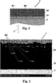
Die Cermetschichten S1 und S2 bestehen jeweils aus einer Mischung aus einer Oxidmatrix mit hoher Brechzahl und einem darin eingelagerten, weniger sauerstoff-affinen Metall. Das hochbrechende Oxid ist entweder Nb2O5 oder TiO2. Das Metall ist Silber oder Kupfer.The cermet layers S1 and S2 each consist of a mixture of an oxide matrix having a high refractive index and a metal which is less oxygen-affixed therein. The high refractive index oxide is either Nb 2 O 5 or TiO 2 . The metal is silver or copper.
Die Cermetschicht S1 besitzt sehr feine Metallausscheidungen M1 mit Durchmessern im Bereich von 3 bis etwa 5 nm, wobei mehr als 90% der Metallausscheidungen M1 einen Durchmesser von weniger als 3 nm haben.The cermet layer S1 has very fine metal precipitates M1 with diameters in the range of 3 to about 5 nm, with more than 90% of the metal precipitates M1 having a diameter of less than 3 nm.
Die Cermetschicht S2 besitzt gröbere Metallausscheidungen M2 mit Durchmessern im Bereich von 4 bis 10 nm, wobei über 90% der Ausscheidungen Durchmesser im Bereich von 2 bis 20 nm haben.The cermet layer S2 has coarser metal precipitates M2 with diameters ranging from 4 to 10 nm, with over 90% of the precipitates having diameters in the range of 2 to 20 nm.
Das Schichtsystem
Die Metallgehalte CM und Schichtdicken d der Cermetschichten S1 und S2 bei den einzelnen Schichtsystemen, die Messwerte für die spezifische Transmission TV und die Reflexion Rv (abzüglich 4% für die Reflexion der unbeschichteten Glasseite) ergeben sich aus der folgenden Tabelle. Tabelle 
Die Qualität des Schichtsysteme wurde hinsichtlich ihrer spektralen Reflexion RV, der spektralen Transmission TV und ihres elektrischen Widerstandes R☐ bewertet. Das Ergebnis ist in Spalten ”Q” angegeben. Dabei setzt sich die Symbolik der qualitativen Bewertung wie folgt um:
- *)
- Schicht erfüllt die gestellten Anforderungen nicht
- **)
- Schicht mit grenzwertigen Eigenschaften
- ohne Angabe:
- Schicht erfüllt die gestellten Anforderungen
- *)
- Layer does not meet the requirements
- **)
- Layer with marginal properties
- without indication:
- Layer meets the requirements
Nachfolgend wird ein Verfahren zur Herstellung der erfindungsgemäßen Schichtstruktur anhand eines Beispiels näher erläutert:
Eine Pulvermischung aus 94 Vol.-% Nb2O4,99 und 6 Vol.-% Ag mit einer mittleren Korngröße von 25 μm wird in einem Taumel-Mischer 1 h intensiv gemischt, so dass sich eine feine und monodisperse Verteilung der Ag-Partikel in Nb2O4,99 ergibt. Anschließend wird diese Mischung in eine Graphitform mit einem Durchmesser von 75 mm und einer Höhe von 15 mmgefüllt. Die Ronde wird durch Heißpressen unter reduzierenden Bedingungen bei 940°C und 20 MPa zu mehr als 85% der theoretischen Dichte verdichtet. Das so erhaltene Gefüge besteht aus einer Nb2O4,99-Matrix, in die einzelne, desagglomerierte Ag-Partikel mit einer mittleren Korngröße von 25 μm eingebettet sind.In the following, a method for producing the layer structure according to the invention is explained in more detail by means of an example:
A powder mixture of 94 vol .-% Nb 2 O 4.99 and 6 vol .-% Ag with a mean particle size of 25 microns is mixed intensively in a tumble mixer for 1 h, so that a fine and monodisperse distribution of Ag Particles in Nb 2 O 4.99 yields. Subsequently, this mixture is filled into a graphite mold with a diameter of 75 mm and a height of 15 mm. The blank is compacted by hot pressing under reducing conditions at 940 ° C and 20 MPa to greater than 85% of the theoretical density. The microstructure thus obtained consists of an Nb 2 O 4.99 matrix in which individual, deagglomerated Ag particles having a mean particle size of 25 μm are embedded.
Analog wird ein zweites Sputtertarget mit 60 Vol.-% Nb2O4,99 und 40 Vol.-% Ag hergestellt.Similarly, a second sputtering target is prepared with 60% by volume Nb 2 O 4.99 and 40% by volume Ag.
Die Sputtertargets weisen einen spezifischen elektrischen Widerstand von weniger als 1 Ohm·cm auf.The sputtering targets have a resistivity of less than 1 ohm.cm.
Unter Verwendung dieser Sputtertargets wird die zweilagige Schichtstruktur
Die Sputterparameter sind dabei wie folgt:
Restgasdruck: 2·10–6 mbar
Prozessdruck: 3·10–3 mbar bei 200 sccm Argon und 1 bis 10 sccm Sauerstoff (entspricht 0,5–5% Sauerstoff im Sputtergas)
Spezifische Kathodenleistung: 5 W/cm2
Schicht S1: Nb2O5 + Ag 6 Vol.-%; d = 38 nm, zusätzlicher Sauerstoffstrom: 1 sccm.
Schicht S2: Nb2O5 + Ag 40 Vol.-%; d = 90 nm, zusätzlicher Sauerstoffstrom: 10 sccm.The sputter parameters are as follows:
Residual gas pressure: 2 · 10 -6 mbar
Process pressure: 3 · 10 -3 mbar at 200 sccm argon and 1 to 10 sccm oxygen (corresponds to 0.5-5% oxygen in sputtering gas)
Specific cathode power: 5 W / cm 2
Layer S1: Nb 2 O 5 +
Layer S2: Nb 2 O 5 + Ag 40% by volume; d = 90 nm, additional oxygen flow: 10 sccm.
Die so hergestellte Schichtstruktur zeichnet sich unter anderem durch folgende Eigenschaften aus:
Schichtwiderstand: 1,3 kΩ/square
Visuelle Reflexion (nach Abzug von ca. 4% Reflexion durch Messung von der unbeschichteten Substratseite): 1,3%.
Visuelle Transmission: kleiner als 1%, typischerweise kleiner als 0,8%The layer structure thus produced is characterized, inter alia, by the following properties:
Sheet resistance: 1.3 kΩ / square
Visual reflection (after subtraction of about 4% reflection by measurement from the uncoated substrate side): 1.3%.
Visual transmission: less than 1%, typically less than 0.8%
Die Absorption der Nb2O5–Ag-Schichtstruktur insgesamt liegt damit höher als 97%. Die Farbe der produzierten Schichtsysteme wird unter Zugrundelegung des CIELab-Farbraummodells ermittelt. Beim „CIELab-Farbraum” werden die gemessenen Spektralkurven auf drei Koordinaten reduziert. Die Koordinatenachsen L*, a*, b* stehen rechtwinkelig aufeinander:
L* beschreibt die Helligkeit von 0 (reines Schwarz) bis 100 (reines Weiß).
a* stellt die Rot-Grün-Achse dar. Negative Werte sind grün, positive sind rot.
b* stellt die Gelb-Blau-Achse dar. Negative Werte sind blau, positive sind gelb.The total absorption of the Nb 2 O 5 -Ag layer structure is thus higher than 97%. The color of the layer systems produced is determined on the basis of the CIELab color space model. In the "CIELab color space", the measured spectral curves are reduced to three coordinates. The coordinate axes L *, a *, b * are perpendicular to each other:
L * describes the brightness from 0 (pure black) to 100 (pure white).
a * represents the red-green axis. Negative values are green, positive are red.
b * represents the yellow-blue axis. Negative values are blue, positive are yellow.
Im CIELab-Farbraum bewegt sich a* im Bereich –1,8 bis +4; und b* zwischen 0 bis –4. Somit ist mit diesem Schichtsystem eine neutrale Reflexionsfarbe auf der unbeschichteten Substratseite einstellbar.In the CIELab color space, a * ranges from -1.8 to +4; and b * between 0 to -4. Thus, a neutral reflection color on the uncoated substrate side is adjustable with this layer system.
Für die gesamte Schichtstruktur
Die
Variante V1Variant V1
- Cermetschicht S1: Dicke 38 nm, Sauerstoff-Fluss beim Sputtern: 1 sccmCermet layer S1: thickness 38 nm, oxygen flux during sputtering: 1 sccm
- Cermetschicht S2: Dicke 88 nm, Sauerstoff-Fluss beim Sputtern: 10 sccm.Cermet layer S2: thickness 88 nm, oxygen flux during sputtering: 10 sccm.
Variante V2Variant V2
- Cermetschicht S1: Dicke 35 nm, Sauerstoff-Fluss beim Sputtern: 0 sccmCermet layer S1: thickness 35 nm, oxygen flux during sputtering: 0 sccm
- Cermetschicht S2: Dicke 88 nm, Sauerstoff-Fluss beim Sputtern: 10 sccm.Cermet layer S2: thickness 88 nm, oxygen flux during sputtering: 10 sccm.
Der Sauerstoff-Fluss beim Sputtern wirkt sich auf die dielektrischen Eigenschaften der Oxidschicht aus. Typischerweise liegt der Sauerstoff-Fluss zwischen 0,5–10% bezogen auf den Gesamtfluss an Sputtergas. Dies ist insbesondere für die Cermetschicht S2 relevant, um eine gute Beständigkeit an Luft zu erreichen.The oxygen flux during sputtering affects the dielectric properties of the oxide layer. Typically, the oxygen flux is between 0.5-10% of the total sputtering gas flow. This is particularly relevant for the cermet layer S2 in order to achieve a good resistance to air.
In
In
Bei Lagerung der Schichtstruktur bei 18–24°C und 50–60% relativer Luftfeuchtigkeit über bis zu 5 Tage haben sich die optischen Eigenschaften nur unwesentlich verändert. Die Änderung von Rv und Tv lag jeweils unter einem Prozentpunkt.When storing the layer structure at 18-24 ° C and 50-60% relative humidity over up to 5 days, the optical properties have changed only slightly. The change in Rv and Tv was below one percentage point each.
Die erfindungsgemäße Schichtstruktur ist wegen ihres hohen Absorptionsvermögens und der geringen elektrischen Leitfähigkeit zur Ausbildung einer Black-Matrix-Schicht für Aktiv-Matrix getriebene Flachbildschirme geeignet.The layer structure according to the invention is suitable for forming a black matrix layer for active matrix driven flat-panel displays because of its high absorption capacity and low electrical conductivity.
ZITATE ENTHALTEN IN DER BESCHREIBUNG QUOTES INCLUDE IN THE DESCRIPTION
Diese Liste der vom Anmelder aufgeführten Dokumente wurde automatisiert erzeugt und ist ausschließlich zur besseren Information des Lesers aufgenommen. Die Liste ist nicht Bestandteil der deutschen Patent- bzw. Gebrauchsmusteranmeldung. Das DPMA übernimmt keinerlei Haftung für etwaige Fehler oder Auslassungen.This list of the documents listed by the applicant has been generated automatically and is included solely for the better information of the reader. The list is not part of the German patent or utility model application. The DPMA assumes no liability for any errors or omissions.
Zitierte PatentliteraturCited patent literature
- US 5976639 A [0004] US 5976639 A [0004]
- US 6387576 B2 [0005] US 6387576 B2 [0005]
Claims (15)
Priority Applications (6)
| Application Number | Priority Date | Filing Date | Title |
|---|---|---|---|
| DE102012010803A DE102012010803A1 (en) | 2012-06-01 | 2012-06-01 | Light absorbing layer structure |
| EP13165729.8A EP2669718B1 (en) | 2012-06-01 | 2013-04-29 | Light absorbing layer structure |
| TW102116696A TWI508862B (en) | 2012-06-01 | 2013-05-10 | Light-absorbing layered structure |
| KR20130061574A KR101489070B1 (en) | 2012-06-01 | 2013-05-30 | Light-absorbing layered structure |
| CN201310211208.3A CN103454708B (en) | 2012-06-01 | 2013-05-31 | Extinction layered structure |
| JP2013117136A JP5675896B2 (en) | 2012-06-01 | 2013-06-03 | Light absorbing layer structure |
Applications Claiming Priority (1)
| Application Number | Priority Date | Filing Date | Title |
|---|---|---|---|
| DE102012010803A DE102012010803A1 (en) | 2012-06-01 | 2012-06-01 | Light absorbing layer structure |
Publications (1)
| Publication Number | Publication Date |
|---|---|
| DE102012010803A1 true DE102012010803A1 (en) | 2013-12-05 |
Family
ID=48366128
Family Applications (1)
| Application Number | Title | Priority Date | Filing Date |
|---|---|---|---|
| DE102012010803A Ceased DE102012010803A1 (en) | 2012-06-01 | 2012-06-01 | Light absorbing layer structure |
Country Status (6)
| Country | Link |
|---|---|
| EP (1) | EP2669718B1 (en) |
| JP (1) | JP5675896B2 (en) |
| KR (1) | KR101489070B1 (en) |
| CN (1) | CN103454708B (en) |
| DE (1) | DE102012010803A1 (en) |
| TW (1) | TWI508862B (en) |
Families Citing this family (3)
| Publication number | Priority date | Publication date | Assignee | Title |
|---|---|---|---|---|
| KR101983691B1 (en) * | 2012-08-17 | 2019-05-30 | 삼성디스플레이 주식회사 | Light blocking member and display panel including the same |
| WO2015135524A1 (en) | 2014-03-13 | 2015-09-17 | Hottinger Baldwin Messtechnik Gmbh | Monolithic miniature broadband light source for measurements by means of fbg strain sensors |
| EP3467140A1 (en) * | 2017-10-06 | 2019-04-10 | Plansee SE | Target material for deposition of molybdenum oxide layers |
Citations (2)
| Publication number | Priority date | Publication date | Assignee | Title |
|---|---|---|---|---|
| US5976639A (en) | 1995-01-11 | 1999-11-02 | Anelva Corporation | Black matrix laminated film and reactive sputtering apparatus |
| US6387576B2 (en) | 1999-12-23 | 2002-05-14 | Samsung Sdi Co., Ltd. | Black matrix and preparing method thereof, and a display device employing the black matrix |
Family Cites Families (5)
| Publication number | Priority date | Publication date | Assignee | Title |
|---|---|---|---|---|
| JPH04342204A (en) * | 1991-05-20 | 1992-11-27 | Matsushita Electric Ind Co Ltd | Black matrix and production thereof |
| KR100615154B1 (en) * | 1999-08-19 | 2006-08-25 | 삼성에스디아이 주식회사 | Cathode layer tube improved in contrast |
| JP4614027B2 (en) | 2000-07-03 | 2011-01-19 | ソニー株式会社 | Optical multilayer structure, optical switching element, and image display device |
| US7332852B2 (en) * | 2004-07-02 | 2008-02-19 | Samsung Electronics Co., Ltd. | One-way transparent optical system having light absorption elements and light refracting structures |
| EP2217865A4 (en) * | 2007-10-18 | 2014-03-05 | Alliance Sustainable Energy | High temperature solar selective coatings |
-
2012
- 2012-06-01 DE DE102012010803A patent/DE102012010803A1/en not_active Ceased
-
2013
- 2013-04-29 EP EP13165729.8A patent/EP2669718B1/en not_active Not-in-force
- 2013-05-10 TW TW102116696A patent/TWI508862B/en not_active IP Right Cessation
- 2013-05-30 KR KR20130061574A patent/KR101489070B1/en not_active IP Right Cessation
- 2013-05-31 CN CN201310211208.3A patent/CN103454708B/en not_active Expired - Fee Related
- 2013-06-03 JP JP2013117136A patent/JP5675896B2/en not_active Expired - Fee Related
Patent Citations (2)
| Publication number | Priority date | Publication date | Assignee | Title |
|---|---|---|---|---|
| US5976639A (en) | 1995-01-11 | 1999-11-02 | Anelva Corporation | Black matrix laminated film and reactive sputtering apparatus |
| US6387576B2 (en) | 1999-12-23 | 2002-05-14 | Samsung Sdi Co., Ltd. | Black matrix and preparing method thereof, and a display device employing the black matrix |
Also Published As
| Publication number | Publication date |
|---|---|
| EP2669718B1 (en) | 2016-12-28 |
| KR20130135766A (en) | 2013-12-11 |
| JP2013250560A (en) | 2013-12-12 |
| CN103454708B (en) | 2016-08-10 |
| EP2669718A1 (en) | 2013-12-04 |
| TWI508862B (en) | 2015-11-21 |
| JP5675896B2 (en) | 2015-02-25 |
| KR101489070B1 (en) | 2015-02-02 |
| TW201412542A (en) | 2014-04-01 |
| CN103454708A (en) | 2013-12-18 |
Similar Documents
| Publication | Publication Date | Title |
|---|---|---|
| EP2912501B1 (en) | Light-absorbing layer system, the production thereof and sputter target suitable therefor | |
| EP2984508B1 (en) | Light-absorbing layer and layer system containing the layer, process for producing the layer system and sputter target suitable therefor | |
| DE10362302B4 (en) | Electromagnetic shielding film product and manufacturing method therefor | |
| DE60029706T2 (en) | TRANSPARENT LIQUID LAMINATE, ITS MANUFACTURING METHOD, AND DISPLAY DEVICE WITH TRANSPARENT CONDUCTIVE LAMINATE | |
| DE69931045T2 (en) | LIGHT ABSORBING ANTI-REFLECTIVE BODIES AND METHOD FOR THE PRODUCTION THEREOF | |
| DE10152412A1 (en) | Film layer with certain optical and electrical properties | |
| DE69815989T2 (en) | DISPLAY DEVICE WITH OPTICAL ELEMENT | |
| EP3391135A1 (en) | Electrically switchable glazing comprising surface electrodes with anisotropic conductivity | |
| EP1829835A1 (en) | Infrared radiation reflecting coating system and method of its production | |
| DE102014111935A1 (en) | Two-layer coating system with partially absorbing layer and process and sputtering target for the production of this layer | |
| DE69734023T2 (en) | Oxide film, laminates and process for their preparation | |
| EP2669718B1 (en) | Light absorbing layer structure | |
| DE10152410A1 (en) | Film layer with certain optical and electrical properties | |
| DE10152411A1 (en) | Film layer with certain optical and electrical properties | |
| DE112014004672T5 (en) | Capacitive touch panel | |
| DE112018006975T5 (en) | Optical thin film, optical element and optical system | |
| DE102009000801A1 (en) | Optical filter and the same display device | |
| DE20221864U1 (en) | Substrate coated with a layer system | |
| WO2012113464A1 (en) | Reflection layer system and method for producing said system | |
| DE102010051259B4 (en) | Method for applying an electrically conductive and optically transparent metal layer, a substrate with this metal layer and its use | |
| WO2009080139A1 (en) | Transparent plastic film for shielding electromagnetic waves and method for producing a plastic film of this type | |
| DE10135126C1 (en) | Filter used as front filter for flat plasma TV screen comprises a layer system formed as alternating layer system consisting of individual layers of metal and metal oxides arranged between two panes | |
| WO2024056340A1 (en) | Composite pane with a heatable reflective layer applied in regions | |
| WO2000026923A1 (en) | Electrically conductive and optically transparent material, method for producing the same and its use | |
| DE102017102569A1 (en) | Layer system with a blackening layer, and method and sputtering target for producing the same |
Legal Events
| Date | Code | Title | Description |
|---|---|---|---|
| R012 | Request for examination validly filed | ||
| R079 | Amendment of ipc main class |
Free format text: PREVIOUS MAIN CLASS: G02B0001100000 Ipc: G02B0001020000 |
|
| R082 | Change of representative |
Representative=s name: STAUDT, ARMIN, DIPL.-ING. (UNIV.), DE |
|
| R081 | Change of applicant/patentee |
Owner name: MATERION ADVANCED MATERIALS GERMANY GMBH, DE Free format text: FORMER OWNERS: FRAUNHOFER-GESELLSCHAFT ZUR FOERDERUNG DER ANGEWANDTEN FORSCHUNG E.V., 80686 MUENCHEN, DE; HERAEUS MATERIALS TECHNOLOGY GMBH & CO. KG, 63450 HANAU, DE Effective date: 20150223 Owner name: HERAEUS DEUTSCHLAND GMBH & CO. KG, DE Free format text: FORMER OWNER: FRAUNHOFER-GESELLSCHAFT ZUR FOER, HERAEUS MATERIALS TECHNOLOGY GM, , DE Effective date: 20150223 Owner name: FRAUNHOFER-GESELLSCHAFT ZUR FOERDERUNG DER ANG, DE Free format text: FORMER OWNER: FRAUNHOFER-GESELLSCHAFT ZUR FOER, HERAEUS MATERIALS TECHNOLOGY GM, , DE Effective date: 20150223 Owner name: HERAEUS DEUTSCHLAND GMBH & CO. KG, DE Free format text: FORMER OWNERS: FRAUNHOFER-GESELLSCHAFT ZUR FOERDERUNG DER ANGEWANDTEN FORSCHUNG E.V., 80686 MUENCHEN, DE; HERAEUS MATERIALS TECHNOLOGY GMBH & CO. KG, 63450 HANAU, DE Effective date: 20150223 Owner name: FRAUNHOFER-GESELLSCHAFT ZUR FOERDERUNG DER ANG, DE Free format text: FORMER OWNERS: FRAUNHOFER-GESELLSCHAFT ZUR FOERDERUNG DER ANGEWANDTEN FORSCHUNG E.V., 80686 MUENCHEN, DE; HERAEUS MATERIALS TECHNOLOGY GMBH & CO. KG, 63450 HANAU, DE Effective date: 20150223 |
|
| R082 | Change of representative |
Representative=s name: KADOR & PARTNER PARTG MBB, DE Effective date: 20150223 Representative=s name: STAUDT, ARMIN, DIPL.-ING. (UNIV.), DE Effective date: 20150223 Representative=s name: KADOR & PARTNER PART MBB PATENTANWAELTE, DE Effective date: 20150223 Representative=s name: KADOR & PARTNER PARTG MBB PATENTANWAELTE, DE Effective date: 20150223 |
|
| R081 | Change of applicant/patentee |
Owner name: FRAUNHOFER-GESELLSCHAFT ZUR FOERDERUNG DER ANG, DE Free format text: FORMER OWNERS: FRAUNHOFER-GESELLSCHAFT ZUR FOERDERUNG DER ANGEWANDTEN FORSCHUNG E.V., 80686 MUENCHEN, DE; HERAEUS DEUTSCHLAND GMBH & CO. KG, 63450 HANAU, DE Owner name: MATERION ADVANCED MATERIALS GERMANY GMBH, DE Free format text: FORMER OWNERS: FRAUNHOFER-GESELLSCHAFT ZUR FOERDERUNG DER ANGEWANDTEN FORSCHUNG E.V., 80686 MUENCHEN, DE; HERAEUS DEUTSCHLAND GMBH & CO. KG, 63450 HANAU, DE |
|
| R082 | Change of representative |
Representative=s name: KADOR & PARTNER PARTG MBB, DE Representative=s name: KADOR & PARTNER PART MBB PATENTANWAELTE, DE Representative=s name: KADOR & PARTNER PARTG MBB PATENTANWAELTE, DE |
|
| R081 | Change of applicant/patentee |
Owner name: MATERION ADVANCED MATERIALS GERMANY GMBH, DE Free format text: FORMER OWNERS: FRAUNHOFER-GESELLSCHAFT ZUR FOERDERUNG DER ANGEWANDTEN FORSCHUNG E.V., 80686 MUENCHEN, DE; MATERION ADVANCED MATERIALS GERMANY GMBH, 63450 HANAU, DE Owner name: FRAUNHOFER-GESELLSCHAFT ZUR FOERDERUNG DER ANG, DE Free format text: FORMER OWNERS: FRAUNHOFER-GESELLSCHAFT ZUR FOERDERUNG DER ANGEWANDTEN FORSCHUNG E.V., 80686 MUENCHEN, DE; MATERION ADVANCED MATERIALS GERMANY GMBH, 63450 HANAU, DE |
|
| R082 | Change of representative |
Representative=s name: KADOR & PARTNER PART MBB PATENTANWAELTE, DE Representative=s name: KADOR & PARTNER PARTG MBB PATENTANWAELTE, DE |
|
| R002 | Refusal decision in examination/registration proceedings | ||
| R003 | Refusal decision now final |